Embed Size (px)
Citation preview
MOS AK
Analysis and modelling of wafer level process variability in advanced FD-SOI devices, using split C-V
and gate current data
Krishna Pradeep1, 2, Theano A. Karatsori2, Thierry Poiroux3, André Juge1, Patrick Scheer1, Gilles Gouget1, and Gérard Ghibaudo2
[email protected], Crolles Site, 850 rue Jean Monnet, 38926 Crolles, France
2IMEP-LAHC, MINATEC Campus, 3 Parvis Louis Néel, 38016 Grenoble, Cedex 1, France3CEA-Leti, MINATEC Campus, 38054 Grenoble Cedex 9, France
MOS AK
Dresden Sept.3, 2017
2/27
Outline
• Introduction.
• Split C-V based process parameter extraction.
• Gate current.
• Statistical modelling.
• Conclusion.

MOS AK
Dresden Sept.3, 2017
3/27
Outline
• Introduction.
• Split C-V based process parameter extraction.
• Gate current.
• Statistical modelling.
• Conclusion.

MOS AK
Dresden Sept.3, 2017
4/27
The concern
• Variability: growing concern with scaling.
– How to effectively account for it in design?

MOS AK
Dresden Sept.3, 2017
5/27
The concern
• Variability: growing concern with scaling.
– How to effectively account for it in design?
• Global• Lot to lot variation.• Wafer to wafer variation.• Die to die variation.
• Local• Intra die variation.

MOS AK
Dresden Sept.3, 2017
6/27
The concern
• Variability: growing concern with scaling.
– How to effectively account for it in design?
• Global• Lot to lot variation.• Wafer to wafer variation.• Die to die variation.
• Local• Intra die variation.

MOS AK
Dresden Sept.3, 2017
7/27
FD-SOI
• Key contender for sub-32 nm nodes.
– Low power, IOT applications, …
L W
Tox (EOT)
TSiTBOX
Planes, N., Weber, O., Barral, V., Haendler, S., Noblet, D., Croain, D., … Haond, M. (2012). 28nm FDSOI technology platform for high-speed low-voltage digital applications. In Digest of Technical Papers - Symposium on VLSI Technology (Vol. 33, pp. 133–134).
Nwell

MOS AK
Dresden Sept.3, 2017
8/27
Outline
• Introduction.
• Split C-V based process parameter extraction.
• Gate current.
• Statistical modelling.
• Conclusion.

MOS AK
Dresden Sept.3, 2017
9/27
Vertical thicknessesAutomated extraction from slope of Qi/C vs Qi plot
0.00 0.01 0.020
1
2
Slope = 1/Cox
Slope = 1/Cb
Qi/C
gc (
V)
Qi (C/m
2)
Vb = 0 V
linear fit
FBB
linear fit
0.000 0.003 0.006 0.009
0
2
4
6
Qi/C
bc (
V)
Qi (C/m
2)
Slope = 1/CBOX
-1.5 -1.0 -0.5 0.0 0.5 1.0 1.5
0.0
0.4
0.8
1.3
1.7
2.1
Cg
c (
F/m
2)
Vg (V)
Vb = 0 V
Vb = 10 Vx 10
-2
High
Vb
Low
-6 -4 -2 0 2 4 6 8 10 12
0.0
0.3
0.7
1.0
1.4
Cb
c (
F/m
2)
Vb (V)
x 10-3
0.4V
High
Low
Pradeep, K., Gouget, G., Poiroux, T., Scheer, P., Juge, A., & Ghibaudo, G. (2017). Systematic evaluation of the split C-V based parameter extraction methodologies for 28 nm FD-SOI. In 2017 International Conference of Microelectronic Test Structures (ICMTS) (pp. 1–5). IEEE.
Cb = series(Cox, CSi)

MOS AK
Dresden Sept.3, 2017
10/27
Vertical thicknessesOn-wafer trends
0 40 80 120 160 200
-3
-2
-1
0
1
2
3
TB
OX (
no
rma
lize
d)
Die No.
NFET
PFET
0 40 80 120 160 200-2
-1
0
1
2
Tox (
no
rmalized
)
Die No.
NFET
PFET
0 40 80 120 160 200
-4
-2
0
2
TS
i (n
orm
alized
)
Die No.
NFET
PFET
Pradeep, K., Gouget, G., Poiroux, T., Scheer, P., Juge, A., & Ghibaudo, G. (2017). Systematic evaluation of the split C-V based parameter extraction methodologies for 28 nm FD-SOI. In 2017 International Conference of Microelectronic Test Structures (ICMTS) (pp. 1–5). IEEE.
Similar trends forPFET and NFET.

MOS AK
Dresden Sept.3, 2017
11/27
0 1
0.8
1.0
1.1x10
-3
Slope=2/(qεNa)
1/C
bg
2 (
m4F
-2)
Vgb
(V)
Ground plane vertical doping profile
•�
����= �
����� + �����
��� − ����[Ghibaudo et. al., T-SM 2000].
• Cbg (Vbg) gives the depletion depth, xdep(Vbg).
• The vertical doping profile obtained by combining these.
Pradeep, K., Gouget, G., Poiroux, T., Scheer, P., Juge, A., & Ghibaudo, G. (2017). Systematic evaluation of the split C-V based parameter extraction methodologies for 28 nm FD-SOI. In 2017 International Conference of Microelectronic Test Structures (ICMTS) (pp. 1–5). IEEE.

MOS AK
Dresden Sept.3, 2017
12/27
Ground plane vertical doping profile
Highly perturbed by measurementnoise, close to accumulation.
0 3 6 9 12
0.4
4
40
We
ll d
op
ing
co
nc
en
trati
on
(n
orm
ali
zed
)
Depth from the BOX interface (nm)
NFET
PFET
Pradeep, K., Gouget, G., Poiroux, T., Scheer, P., Juge, A., & Ghibaudo, G. (2017). Systematic evaluation of the split C-V based parameter extraction methodologies for 28 nm FD-SOI. In 2017 International Conference of Microelectronic Test Structures (ICMTS) (pp. 1–5). IEEE.

MOS AK
Dresden Sept.3, 2017
13/27
Lateral dimensions
• ∆��� = ��� �� = �� + ����� −��� �� = �� − ����� .
– �� is the threshold voltage.
• ∆��� = �"#�"#
(% − ∆%)(' − ∆').• Linear regression with W (for
constant L) and L (for constant W).
• Lov from overlap component of parasitic capacitance.
Leff
Polyepi Lov
Lpoly
L=Ldesign*shrinkSource Drain
Gate
∆L/2∆L/2
Conta
ct
Conta
ct
%(�� = %)(*+�, × �./012 − ∆%'(�� = ')(*+�, × �./012 − ∆'
%3456 = %(�� + 2%48
Pradeep, K., Gouget, G., Poiroux, T., Scheer, P., Juge, A., & Ghibaudo, G. (2017). Systematic evaluation of the split C-V based parameter extraction methodologies for 28 nm FD-SOI. In 2017 International Conference of Microelectronic Test Structures (ICMTS) (pp. 1–5). IEEE.
MOS AK
Dresden Sept.3, 2017
14/27
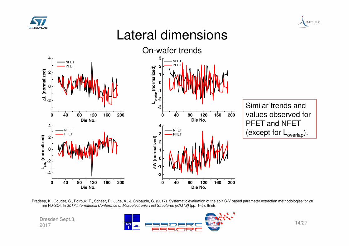
Lateral dimensionsOn-wafer trends
0 40 80 120 160 200
-3
-2
-1
0
1
2
3
Lo
ve
rla
p (
no
rma
lize
d)
Die No.
NFET
PFET
0 40 80 120 160 200
-4
-2
0
2
4
Lp
oly (
no
rma
lize
d)
Die No.
NFET
PFET
0 40 80 120 160 200
-2
0
2
4
∆L (
no
rma
lize
d)
Die No.
NFET
PFET
0 40 80 120 160 200
-2
-1
0
1
2
3
4
∆W (
no
rma
lize
d)
Die No.
NFET
PFET
Similar trends and values observed for PFET and NFET (except for Loverlap).
Pradeep, K., Gouget, G., Poiroux, T., Scheer, P., Juge, A., & Ghibaudo, G. (2017). Systematic evaluation of the split C-V based parameter extraction methodologies for 28 nm FD-SOI. In 2017 International Conference of Microelectronic Test Structures (ICMTS) (pp. 1–5). IEEE.

MOS AK
Dresden Sept.3, 2017
15/27
Outline
• Introduction.
• Split C-V based process parameter extraction.
• Gate current.
• Statistical modelling.
• Conclusion.

MOS AK
Dresden Sept.3, 2017
16/27
Equivalent single trapezoidal barrier model
• 9� = � × :+; × <= × ' × %.• Gate transparency modelled
using an equivalent single trapezoidal barrier.
– Thickness: 4? × @A.
– Barrier height: A × C4?.
– <= = �DE − F"#GH IJ"#
+ K�LF"#� GH�MN��J"#O"# I .
• P4? = ��.Q×H"# O"#
.
0.0 0.3 0.6 0.9 1.210
-14
10-11
10-8
I g (
A)
Vg (V)
2/10_Expt.
2/10_Model
2/0.3_Expt.
2/0.3_Model
28 nm FD-SOIHK = 1.9A = 0.39
0.0 0.3 0.6 0.910
-17
10-13
10-9
I g (
A)
Vg (V)
0.3/0.35_Expt.
0.3/0.35_Model
0.06/0.02_Expt.
0.06/0.02_Model
14 nm FD-SOIHK = 1.52A = 0.5
Pradeep, K., Karatsori, T. A, Poiroux, T., Juge. A, Scheer, P., Gouget, G., Josse E. , & Ghibaudo, G. Analysis of Gate Current Wafer Level Variability in Advanced FD-SOI MOSFETs. 2018 ESSDERC

MOS AK
Dresden Sept.3, 2017
17/27
tIL, tHK variance segregation using C-V & Ig
• Using ln T�K�
= ln� + ln<=:
– Intercept of linear fit of ln <= with :+: − FUV
JUV− FWX
JWX.
• PTY ZT,F(=�(3F = ZFUV + JUV
JWX
ZFWX .
• From split C-V:
– ZF"# = ZFUV
+ NUVNWX
ZFWX .
• Can extract ZFUV & ZFWX from these.
0.0 0.5 1.0 1.5 2.0 2.5
104
105
106
Linear fit
Expt.
I g/Q
i (A
/C)
Qi x 10
-13 (C)
• 28 nm FD-SOI:• W/L = 2 µm/10 µm.• ZFUV = 0.0041].
• ZFWX = 0.0141].
• 14 nm FD-SOI:• W/L = 5 µm/5 µm.• ZFUV = 0.0051].• ZFWX = 0.0921].
Pradeep, K., Karatsori, T. A, Poiroux, T., Juge. A, Scheer, P., Gouget, G., Josse E. , & Ghibaudo, G. Analysis of Gate Current Wafer Level Variability in Advanced FD-SOI MOSFETs. 2018 ESSDERC

MOS AK
Dresden Sept.3, 2017
18/27
Outline
• Introduction.
• Split C-V based process parameter extraction.
• Gate current.
• Statistical modelling.
• Conclusion.

MOS AK
Dresden Sept.3, 2017
19/27
Statistical modelling of global variability
• For any property X of the device whose variability is being studied.– ∆X/X ≡ ln (X/X0) where X0 is the property of the device at the center of the wafer.
– Standard deviation, σ(∆X/X).
– Z ∆aa
= ∑ c5,acde
Z(fg) de .
• Sensitivity to each parameter: hi� c jk acd�
.
• Percentage contributions:
– %f+ = c 5, a cd�⁄ �n� d�∑ c 5, a cde⁄ �n� dee
× 100.
• This can be applied to capacitance.– Using Leti-UTSOI compact model.
• This can be applied to gate current.– Using equivalent single trapezoidal barrier model.
Pradeep, K., Poiroux, T., Scheer, P., Gouget, G., Juge, A., & Ghibaudo, G. (2017). Sensitivity analysis of C-V global variability for 28 nm FD-SOI. In 2017 Joint
International EUROSOI Workshop and International Conference on Ultimate Integration on Silicon (EUROSOI-ULIS) (pp. 132–135). IEEE.

MOS AK
Dresden Sept.3, 2017
20/27
0.4 0.6 0.8 1.0 1.2 1.410-5
10-4
10-3
σ2 (∆C
/C)
Vg (V)
measure
model
0.0 0.3 0.6 0.9 1.2
10-5
10-4
10-3
10-2
10-1
σ2 (∆C
/C)
Vg (V)
measure
model
-0.8 -0.4 0.0 0.4 0.8 1.2
10-5
10-4
10-3
10-2
10-1
σ2 (∆C
/C)
Vg (V)
measure
model
Capacitance statistical modelLong-wide NFET
Vb = 0 V Vb = 5 V
Vb = 10 V
Z ∆��
= o pq1�
pfg Z(fg)
de
• Good fit obtained with the model.
• Fitted values close to initial guesses.
Pradeep, K., Poiroux, T., Scheer, P., Gouget, G., Juge, A., & Ghibaudo, G. (2017). Sensitivity analysis of C-V global variability for 28 nm FD-SOI. In 2017 Joint
International EUROSOI Workshop and International Conference on Ultimate Integration on Silicon (EUROSOI-ULIS) (pp. 132–135). IEEE.
Parameters used:Vfb, Vfbb, TSi, TBOX, Tox, ln Nwell

MOS AK
Dresden Sept.3, 2017
21/27
0.0 0.4 0.8 1.20
20
40
60
80
100
% c
on
trib
uti
on
Vg (V)
Tox
TSi
TBOX
Vfb
0.6 0.8 1.0 1.20
20
40
60
80
100
% c
on
trib
uti
on
Vg (V)
Tox
TSi
TBOX
Vfb
0.2 0.4 0.6 0.8 1.0 1.20
20
40
60
80
100
% c
on
trib
uti
on
Vg (V)
Tox
TSi
TBOX
Vfb
Capacitance percentage contributions
• Tox dominant in strong
inversion.
• RBB, moderate inversion:
Vfb dominant.
– Even stronger at Vb = 0 V.
• Very strong FBB, moderate
inversion: TSi dominant.
Long-wide NFET
Vb = 0 VVb = -5 V
Vb = 5 V
%f+ = p q1 � pf+⁄ Z f+∑ p q1 � pfg⁄ Z fgg
× 100
Pradeep, K., Poiroux, T., Scheer, P., Gouget, G., Juge, A., & Ghibaudo, G. (2017). Sensitivity analysis of C-V global variability for 28 nm FD-SOI. In 2017 Joint
International EUROSOI Workshop and International Conference on Ultimate Integration on Silicon (EUROSOI-ULIS) (pp. 132–135). IEEE.

MOS AK
Dresden Sept.3, 2017
22/27
Ig statistical model
• The proposed model can reproduce the measured variance quite well.
• Parameters used:
– VT.
– tox.
14 nm FD-SOI
0.2 0.4 0.6 0.8 1.010
-1
100
σ2 (∆I g
/Ig)
Vg (V)
Expt.
Model
σtox
= 0.04 nm
σVT
= 0.029 V
Pradeep, K., Karatsori, T. A, Poiroux, T., Juge. A, Scheer, P., Gouget, G., Josse E. , & Ghibaudo, G. Analysis of Gate Current Wafer Level Variability in Advanced FD-SOI MOSFETs. 2018 ESSDERC

MOS AK
Dresden Sept.3, 2017
23/27
Ig percentage contributions
• Above threshold, the Ig variation is controlled almost completely by the barrier thickness.
• Below threshold, both VT and barrier thickness have similar contributions.
– VT slightly dominating barrier
thickness.
14 nm FD-SOI
0.0 0.3 0.6 0.90
25
50
75
100
% c
on
trib
uti
on
Vg (V)
tox
VT
Pradeep, K., Karatsori, T. A, Poiroux, T., Juge. A, Scheer, P., Gouget, G., Josse E. , & Ghibaudo, G. Analysis of Gate Current Wafer Level Variability in Advanced FD-SOI MOSFETs. 2018 ESSDERC

MOS AK
Dresden Sept.3, 2017
24/27
Outline
• Introduction.
• Split C-V based process parameter extraction.
• Gate current.
• Statistical modelling.
• Conclusion.

MOS AK
Dresden Sept.3, 2017
25/27
Conclusions
• Robust, efficient split C-V parameter extraction methods.– Automated extraction on large amount of measurement
data.
• Gate leakage current model proposed.– Shown to work in different technology nodes and different
geometries.
– Can extract variance of IL and HK layers.
• Statistical model.– Works for both capacitance and Ig wafer level global
variability.
– Can analyse the dominant source of variability at each bias condition.
– Can be further extended to Id or any other property, using Leti-UTSOI compact model.

MOS AK

MOS AK

MOS AK
Appendix

MOS AK
Dresden Sept.3, 2017
29/27
Calibrated Leti-UTSOILong-wide NFET
-1.5 -1.0 -0.5 0.0 0.5 1.0 1.5
0.0
0.4
0.8
1.2
1.6
2.1
2.5
-1.5 -1.0 -0.5 0.0 0.5 1.0 1.5V
g (V)
UTSOI Measure
Vb = -5 V
Vb = 0 V
Vb = 2 V
Vb = 5 V
Vb = 10 V
x 10-2
Cg
c (
F/m
2) • Good fit of the
measurements obtainedwith Leti-UTSOI at differentVb values.
• Used to calculate thesensitivities.
Pradeep, K., Poiroux, T., Scheer, P., Juge, A., Gouget, G., & Ghibaudo, G. (2018). Analysis and modeling of wafer-level process variability in 28 nm FD-SOI using split C-V measurements. Solid-State Electronics, 145(March), 19–28.

MOS AK
Dresden Sept.3, 2017
30/27
Percentage contribution of TSi
• The change in the sign
of sensitivity around
the threshold voltage.
– Responsible to make the contribution go to zero at this bias.
Leti-UTSOI results
-1.5 -1.0 -0.5 0.0 0.5 1.0 1.5-0.3
0.0
0.3
0.6
0.9
1.2
1.5
1.9
2.2
2.5
Cc
g (
F/m
2)
Vg (V)
TSi = 6 nm
TSi = 6.6 nm
x 10-2