Embed Size (px)
Citation preview

Dr.A.Arul Lawrence selvakumar /International Journal of Engineering and Technology Vol.1(2), 2009, 50-62
50
Analysis & Design of Network in Reusable Sub-Systems
Dr.A.Arul Lawrence selvakumar, Professor & Head
Madanapalle Institute of Technology & Science [email protected], [email protected]
Abstract: Models of computation (MOC) provide a framework to model various algorithms and activities, while accounting for and exploiting concurrency and synchronization aspects.. Further, a combination of these MOCs may be needed to truly represent a given Network-onChip (NOC) region and may further differ from a global to a local region. We have analyzed various models of computation (MOC) suitable for NoC. We have modeled a concurrent architecture for a customizable and scalable NOC in a system-level modeling environment using MLDesigner. MLDesigner provides a system level modeling platform, which allows one to integrate such MOCs together. We provide simulation results for various scheduling criteria, injection rates, buffer sizes, and network traffic. We abstracted area results for a 4×4 mesh based NoC from its Field Programmable Gate Arrays (FPGA) implementation. We have further quantified all the results and presented them from a system architect’s view.
I. INTRODUCTION A system design process is inherently complex.
The design involves multiple representations, multiple (design) groups working on different design phases, and a complex hierarchy of data and applications [1]. The different groups bring different perspectives towards system design. The system or product inconsistencies primarily arise out of lack of appropriate communication among various design teams. For example, concerns of a hardware (HW) design engineer are different from that of a software (SW) designer and they are often unable to understand and help address the problems of the other [2]. Such constraints lead to increase in product development cycle and product development cost, thereby reducing system design productivity [3]. To enhance this declining productivity, one will have to exploit the principle of “design-and-reuse” to its full potential [4]. Then, a system (subsystem) would be composed of reusable sub-systems (components).
Network-on-Chip (NoC) architecture can improve this declining design productivity by serving as a reusable communication sub-system for an embedded device [5]. NoC provides an multi-core architecture
for managing complexity by incorporating concurrency and synchronization. This NoC architecture may comprise of components such as, routers, input and output buffers, network interface, switch, virtual channel allocator, scheduler and a switch allocator [6]. To develop a system from such reusable components, one will have to design and develop variants of each component. For example, buffer size is a customizable parameter for an input buffer. Similarly, scheduling criteria provides customizability for scheduler component. A system architect estimates performance and Quality-of-service (QoS) parameters for various system configurations. Components need to encapsulate their performance metrics for various useful parameter combinations, in order to help the architect to make informed decisions. We propose that a system be modeled in advance of the architect’s design phase. Such a model is analyzed to ensure system functionality at an abstract manner. This model can then be ported to architect’s design phase, for analyzing the performance of a system and for estimating the resources needed for mapping an application on to the system. This model must allow one to manipulate a set of parameters to fine tune system performance. Such a system model needs to have high level representation of various performance and QoS parameters for subsystems and components. These performance and QoS parameters can then be traded-off against each other in the system model, to yield a global optimization. Such a model at the design phase will allow one to make key decisions and reduce the scope of the multidimensional search space. These key decisions may include the number of processors, HW-SW partitioning, estimated performance values for new components, and the use of existing components in SW or HW. Such design decisions have the potential to significantly enhance productivity of system design.
Such system modeling, analysis and design will not be an effective solution until we have a mechanism for modeling of concurrency and synchronization issues [7]. This requires representation of various activities and algorithms

Dr.A.Arul Lawrence selvakumar /International Journal of Engineering and Technology Vol.1(2), 2009, 50-62
51
with appropriate MOC (Models of Computation) [8]. This defines our two goals for the system level designers: (1) To model the system functionality well in advance of building the actual computing system in order to provide a level of flexibility in system design. (2) To be able to manipulate an abstract set of design elements simultaneously to generate different sets of QoS (Quality of Service) parameters and performance metrics and fine tune the system model.
A MOC is a mathematical formalism that captures and allows us to reason about a computational system or concept independent of its implementation details. Different MOCs have evolved to represent the reasoning in different areas of focus [9]. A synchronous local region of an NoC might require one or more such MOCs to co-exist and interact. Further, to reduce simulation time and to integrate the subsystems into an integrated system model, other MOCs may be needed. Thus, several MOCs are needed for modeling an integrated system [10]. In such a system each component or the subsystem of the system should be able to use any allowed MOC and more importantly should retain its behavior after integration of the system. Consider also the case in which a subsystem uses two or more local regions (or islands) of the NoC. These are connected by a switch in an NoC. For example consider a digital camera as a component, or as a subsystem of a much larger system, such as a wireless handheld device (system). It is possible that its design would not fit into one local region. Under such a scenario we should also be able to address the concurrency and synchronization issues because of shared resources (both local and global). We have integrated appropriate models of computation to model our NoC architecture.
In this paper we discuss various MOCs that can be used for modeling NoC architecture. We present a system-level model of the our NoC, called ONoC, after our Motorola funded project entitled “One Pass
to Production,” where our goal is to develop a seamless integrated methodology for developing a mobile embedded system . ONoC is a quality-of-service driven, customizable, and parametriziable NoC implementation. We have combined different MOCs together to represent NoC model. ONoC model has been tested for different injection rates and distribution patterns. We provide latency results for different buffer sizes, scheduling algorithms, and NoC area. We abstracted area results from its FPGA implementation.
1.1 NOC Architecture Description
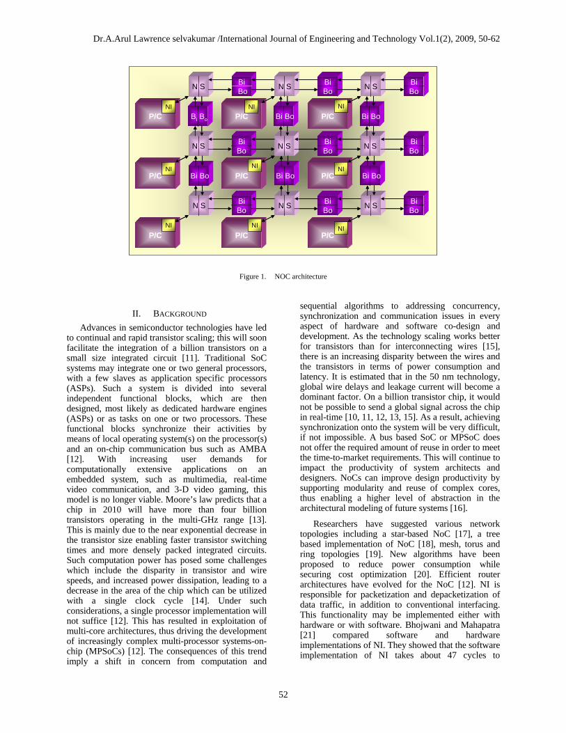
A NoC is designed as a layered architecture and mainly comprises of two layers: communication protocol and communication backbone. Communication Protocol layer consists of the Network Interface (NI) and is responsible for decoupling communication from computation and packetization/depacketization. The Communication Backbone layer, on the other hand, is instantiated with three components: routers, buffers and links. Figure 1 shows a 3×3 mesh based NOC architecture. In Figure 1, Bi, Bo, P, C, N, S and NI represent input buffer, output buffer, producer, consumer, node, scheduler and network interface respectively. Links provide connection to various buffers, node/scheduler, and buffer. The routers are connected to each other and to NI, as per a specific topology. The router block includes the Node (N) and the Scheduler (S). S is responsible for controlling the traffic flow while the actual data is router via a N. The Communication Backbone layer supports routing, switching priority based communication, and flow control logic. A resource such as processor, memory, field programmable gate array (FPGA), application specific integrated circuit (ASIC), or any other hardware element, must be connected to routers or switches through an NI.
Dr.A.Arul Lawrence selvakumar /International Journal of Engineering and Technology Vol.1(2), 2009, 50-62
52
P/C
N S N S N S
Bi Bo
N S
Bi Bo
N S
Bi Bo
N S
Bi Bo
N S
Bi Bo
N S
Bi Bo
N S
BiBo
BiBo
BiBo
BiBo
BiBo
BiBo
BiBo
BiBo
BiBo
P/C
P/C P/C
P/C
P/C
P/C P/C P/C
P/C
N S N S N S
Bi Bo
N S
Bi Bo
N S
Bi Bo
N S
Bi Bo
N S
Bi Bo
N S
Bi Bo
N S
BiBo
BiBo
BiBo
BiBo
BiBo
BiBo
BiBo
BiBo
BiBo
P/C
P/C P/C
P/C
P/C
P/C P/C P/C
NI NI
NI NI
NI
NI
NI
NI
NI
Figure 1. NOC architecture
II. BACKGROUND Advances in semiconductor technologies have led
to continual and rapid transistor scaling; this will soon facilitate the integration of a billion transistors on a small size integrated circuit [11]. Traditional SoC systems may integrate one or two general processors, with a few slaves as application specific processors (ASPs). Such a system is divided into several independent functional blocks, which are then designed, most likely as dedicated hardware engines (ASPs) or as tasks on one or two processors. These functional blocks synchronize their activities by means of local operating system(s) on the processor(s) and an on-chip communication bus such as AMBA [12]. With increasing user demands for computationally extensive applications on an embedded system, such as multimedia, real-time video communication, and 3-D video gaming, this model is no longer viable. Moore’s law predicts that a chip in 2010 will have more than four billion transistors operating in the multi-GHz range [13]. This is mainly due to the near exponential decrease in the transistor size enabling faster transistor switching times and more densely packed integrated circuits. Such computation power has posed some challenges which include the disparity in transistor and wire speeds, and increased power dissipation, leading to a decrease in the area of the chip which can be utilized with a single clock cycle [14]. Under such considerations, a single processor implementation will not suffice [12]. This has resulted in exploitation of multi-core architectures, thus driving the development of increasingly complex multi-processor systems-on-chip (MPSoCs) [12]. The consequences of this trend imply a shift in concern from computation and
sequential algorithms to addressing concurrency, synchronization and communication issues in every aspect of hardware and software co-design and development. As the technology scaling works better for transistors than for interconnecting wires [15], there is an increasing disparity between the wires and the transistors in terms of power consumption and latency. It is estimated that in the 50 nm technology, global wire delays and leakage current will become a dominant factor. On a billion transistor chip, it would not be possible to send a global signal across the chip in real-time [10, 11, 12, 13, 15]. As a result, achieving synchronization onto the system will be very difficult, if not impossible. A bus based SoC or MPSoC does not offer the required amount of reuse in order to meet the time-to-market requirements. This will continue to impact the productivity of system architects and designers. NoCs can improve design productivity by supporting modularity and reuse of complex cores, thus enabling a higher level of abstraction in the architectural modeling of future systems [16].
Researchers have suggested various network topologies including a star-based NoC [17], a tree based implementation of NoC [18], mesh, torus and ring topologies [19]. New algorithms have been proposed to reduce power consumption while securing cost optimization [20]. Efficient router architectures have evolved for the NoC [12]. NI is responsible for packetization and depacketization of data traffic, in addition to conventional interfacing. This functionality may be implemented either with hardware or with software. Bhojwani and Mahapatra [21] compared software and hardware implementations of NI. They showed that the software implementation of NI takes about 47 cycles to

Dr.A.Arul Lawrence selvakumar /International Journal of Engineering and Technology Vol.1(2), 2009, 50-62
53
complete packetization/depacketization, while the hardware version takes only 2 cycles. Substantial research has been conducted to propose the right data formats needed for various layers in the protocol stack. Ethereal [23] and XPIPES [5], [23] NOCs use OCP protocol, while SPIN [24] and Proteo [25] NOCs have integrated Virtual Component Interface (VCI) protocol in their implementations. Various routing algorithms have been proposed for the NoC environment. Most of the researchers suggested static routing algorithms and have performed communication analysis for NoC based on static behavior of the processes, thus obtaining a static routing for NoC. Siebenborn et. al. used a communication dependency graph (CDG) to analyze inter-process communication [26]. Hu et. al. provided graph-based application decomposition and mapping strategies for NoC [27]. Madsen et. al. provided a real-time operating system (RTOS) architecture for NoC [28]. They provided RTOS-based application scheduling techniques for use on a NoC. Based on routing strategies, various router implementations have also been proposed. Wolkotte et. al. proposed a circuit switched router architecture for NoC [29]. Dally and Towles proposed router architecture for packet-based switching [15]. The design of virtual channels is another important aspect of NoC. A virtual channel splits a single channel into two (or more) channels, virtually providing two (or more) paths for the packets to be routed over. Bjerregaard and Sparso implement a virtual channel router using asynchronous circuit techniques [30]. Another important aspect of NoC is the design of interconnects. Brager et. al. propose transmission line based design of interconnects for NoC [31]. Morgenshtein et. al. provided a comparative analysis for serial and parallel links for interconnect implementation [32]. Bertozzi et. al. proposed error detection and correction schemes for data on NoC links [33]. Lee et. al. propose an integrated NoC implementation [34].
III. MOCS FOR MODELING NOC In this section, we address below the various
MOCs needed to model NoC.
3.1 NOC at System Level (Global Region)
At the system (top) level, the NoC model must be defined at a high level of abstraction for it to be useful for performance evaluation. Lower level (RTL (Register transfer Level) code, VLSI (Very large Scale Integration), and Source code) issues, while appropriate for the design level, would slow down the trade-off analysis. Assume that a digital camera’s processing is implemented on an NoC; then the system level issues to be addressed would be resolution, image size, power dissipation and cost, which we would refer to as parameters. We should be able to adjust one of these parameters to fine tune
system performance and yield different combinations of cost-performance-QoS-power dissipation. One may wish to do this on a dynamic basis for better power management of the system in the field. Thus, we can argue that at system level we would need some a kind of a manager to dynamically optimize the system level design parameters.
At the same time such a control (manager) should have some level of concurrency in time domain. This is due to the fact that control (manager) might have to optimize two or more different local regions at the same time. This requirement rules out a finite state machine (FSM) model to sit at the top as a manager. At the system level this manager should be able to observe and control only those signals, which are changing their state or behavior rather than monitoring all the signals at every clock event. A discrete event simulation at the system level would suite such a requirement.
Another possible MOC to model global communication and management in NoC, with asynchronous mechanisms, is the process network (PN). This MOC was described by Kahn and McQueen. Two important properties of the PN domain which make such computation plausible are that processes communicate asynchronously and that the memory used in the communication is unbounded. Any practical implementation of PN cannot support an infinite memory requirement; therefore we specify upper bound for memory requirements whenever possible. The PN domain has the capability to model a system as a network of processes that communicate with each other by passing messages through unidirectional first-in-first-out channels.
3.2 NoC at Subsystem Level (Local Region)
The local region for NoC is again divided into two different domains as NoC at subsystem level and NoC at component level. At sub-system level we address local issues (as relating to a particular subsystem) rather than the global issues. Such a sub-system will usually be some DSP sub-system, IP-core, FPGA, or application specific integrated circuit (ASIC). This subsystem in conjunction with the packet switching network would be required to consume some fixed amount of data (tokens) at the input and to produce some fixed amount of data (tokens) at output that will be routed over the network. Synchronous data flow (SDF) is one such MOC which has appropriate properties. At subsystem level, there is also some need for a small control element. This control element would be required to address the synchronization issue at that subsystem level only, making FSM as another feasible MOC for the subsystem level.
3.3 NoC at Component Level (Local Region)
A component is another essential part of the local region. These components together would constitute

Dr.A.Arul Lawrence selvakumar /International Journal of Engineering and Technology Vol.1(2), 2009, 50-62
54
the higher subsystem level. At this level designer will not have to worry about addressing the system wide concurrency and synchronization issues and the design should be highly reusable to be able to be utilized in other products and scalable to be mapped into the higher domains, viz., the subsystems and the systems. This component level would comprise of software components, and a computation part which in turn could be represented by electronic components and computer architecture components. For electrical components to be specified in such domain, we can use mathematical equations to represent properties of the model; continuous time (CT) MOC is a feasible solution here. Hierarchical FSM can contribute to synchronization among the software elements and the hardware components at component level where each state can be programmable in itself. Such a state machine is often referred as a state chart, where each state has trigger, action and guard conditions. At the same time we may also utilize SDF MOC to model the architectural issues.
IV. ONOC CUSTOMIZABLE PARAMETERS ONoC model support component customization.
This customization has been provided in the form of a drop-down menu. Such facility eases the task of a design architect. He/she can now change the actual system model to understand the impact of various design parameters without the need for changing the actual design. Thus, it has potential to provide a more effective analysis of the result by investing less time as compared to the traditional ways of performance analysis. These customization parameters are discussed below:
4.1 Buffer Size
We can change the buffer size to any value. By changing the buffer size, we can understand its impact on latency, area and therefore the silicon cost.
4.2 Priorities
We provided three priority levels for data packets in our ONoC model: High priority, Mid priority and Low priority. High priority supports control signals such as Read (RD), Write (WR), Acknowledge (ACK), and interrupts. Therefore, high priority data is a short packet (single flit packet). Mid priority supports real-time traffic on the system, while Low priority supports non-real time block transfers of data packets. We have defined control signals as a high priority because the data must respond to a right control signal. Therefore, a control signal must reach its destination in time to manage the communication flow of the network. Equally important is to ensure the delivery of real-time data in real-time bounds. Therefore, we have assigned Mid Priority to real-time data. Rest of the data on the network belongs to low
priority class of data traffic. Number of priority levels is a customizable parameter.
4.3 Input and Output Buffer Scheduling Criteria
Buffer forwards the data to the next block based on its scheduling criteria. We provided three scheduling criteria (also referred as service levels (SL)): First-Come-First-Serve (FCFS), Priority Based (PB), and Priority-Based-Round-Robin (PBRR).
4.4 Scheduler Scheduling Criteria
Scheduler also supports different scheduling criteria. Thus, in a network we can have a combination of scheduling algorithms. Scheduler supports FCFS, Round-Robin (RR), PB, and PBRR. A scheduler is connected with five Input Buffers and five Output Buffers.
4.5 Routing Algorithm
Routing algorithms is another important parameter. There are three different routing algorithms included in the model. These algorithms are: X-Direction First, Y-Direction First and XY-Random.
4.6 Packet Injection Rate
Packet Injection Rate represents the number of flits per cycle injected into the network for transmission. We have defined it as a customizable parameter to test our ONoC model for varying load conditions. Injection rate is changed from 0.1 to 1.0 at equal increments of 0.1 to check the resultant network latency. An injection rate of 1.0 represents that a producer class outputs a flit every clock cycle. Similarly, a rate of 0.33 represents the injection of a flit in every three clock cycles.
V. ONOC MODEL ONoC has been designed in an object oriented
manner. In this section we discuss our ONoC model and its classes.
5.1 Producer Class
Producer comprises a resource and a resource network interface. Producer generates the required traffic pattern and packetizes the data into flits. A flit is the smallest unit of communication supported in ONoC. The customizable parameters for Producer are: (1) The distribution pattern of the data; (2) Amount of data generated as a function of time (throughput); (3) Priorities of the generated data - High, Mid or Low; and (4) The source and the destination addresses for the data (route information).
We used three statistically generated traffic distribution patterns – uniform traffic with linear destination, random and application specific patterns. Producer outputs a flit when buffAvail is asserted by
Dr.A.Arul Lawrence selvakumar /International Journal of Engineering and Technology Vol.1(2), 2009, 50-62
55
Buffer. A flit is time-stamped at the time of its generation. The timestamp is used to determine the latency involved in delivering the flit. The source and destination address fields of the flit header are updated at this time. Flit header has fields for its priority, timestamp, x-direction of source address, y-direction of the source address, x-direction of the destination address, and the y-direction of the destination address. The priority of this flit is governed as per a statistical distribution block. For example, in case of a uniform distribution pattern, every third flit will be a high priority flit. Once the new flit has its timestamp, source and destination address and priority fields updated, it is then forwarded to the output through dataOut. Producer class has been implemented with SDF MOC as it is responsible for continuous data flow.
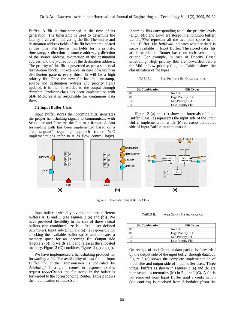
5.2 Input Buffer Class
Input Buffer stores the incoming flits, generates the proper handshaking signals to communicate with Scheduler and forwards the flits to a Router. A data forwarding path has been implemented based on a “request-grant” signaling approach (other NoC implementations refer to it as flow control logic).
Incoming flits corresponding to all the priority levels (High, Mid and Low) are stored in a common buffer. Let buffSize represent all the available space in an Input Buffer. The buffAvail indicates whether there is space available in Input Buffer. The stored data flits are forwarded to Router based on their scheduling criteria. For example, in case of Priority Based scheduling, High priority flits are forwarded before the Mid or Low priority flits, etc. Table 1 shows the classification of flit types.
TABLE I. FLIT PRIORITY BIT COMBINATIONS
Bit Combination Flit Types
00 No Flit 01 High Priority Flit 10 Mid Priority Flit 11 Low Priority Flit
Figure 2 (a) and (b) show the internals of Input Buffer Class. (a) represents the input side of the Input Buffer implementation while (b) represents the output side of Input Buffer implementation.
(a) (b) (c)
Figure 2. Internals of Input Buffer Class
Input buffer is virtually divided into three different
buffers A, B and C (see Figures 2 (a) and (b)). We have provided flexibility in the size of these virtual buffers (the combined size is a fixed user defined parameter). Input side (Figure 2 (a)) is responsible for checking the available buffer space and allocates a memory space for an incoming flit. Output side (Figure 2 (b)) forwards a flit and releases the allocated memory. Figure 2 (C) combines Figures 2 (a) and (b).
We have implemented a handshaking protocol for forwarding a flit. The availability of data flits in Input Buffer for further transmission is indicated by dataInBuff. If a grant comes in response to this request (nodeGrant), the flit stored in the buffer is forwarded to the corresponding Router. Table 2 shows the bit allocation of nodeGrant.
TABLE II. NODEGRANT BIT ALLOCATION
Bit Combination Flit Types
00 No Flit 01 High Priority Flit 10 Mid Priority Flit 11 Low Priority Flit On receipt of nodeGrant, a data packet is forwarded by the output side of the input buffer through dataOut. Figure 2 (c) shows the complete implementation of input side and output side of input buffer class. Three virtual buffers as shown in Figures 2 (a) and (b) are represented as memories (M) in Figure 2 (C). A flit is not removed from Input Buffer until a confirmation (via confirm) is received from Scheduler (from the
Dr.A.Arul Lawrence selvakumar /International Journal of Engineering and Technology Vol.1(2), 2009, 50-62
56
output side of Figure 2 (C)). If confirm is not received, the data flit is not removed from Input Buffer; however, it will be queued for later forwarding. We provided three virtual channels per buffer. A VC controller inside input buffer updates these virtual channels. We implemented input buffer class with DE MOC. DE domain facilitates signaling protocol thus, an ideal choice for implementing handshaking protocols. 5.3 Scheduler Class
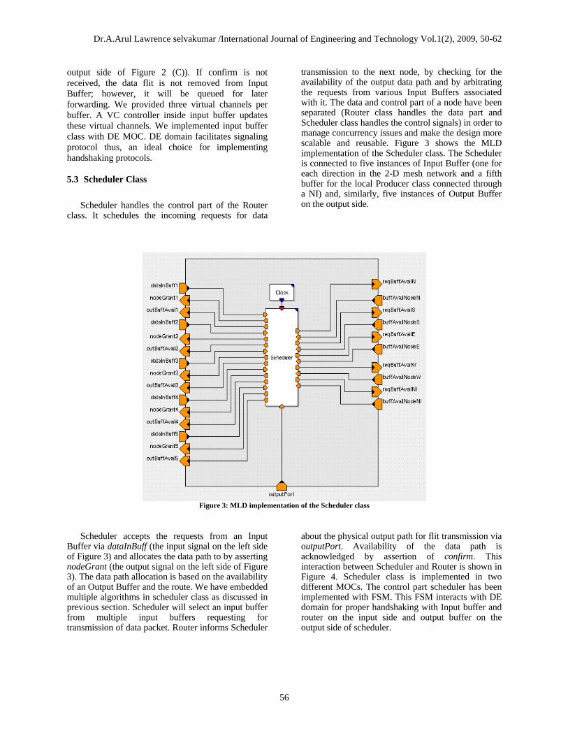
Scheduler handles the control part of the Router class. It schedules the incoming requests for data
transmission to the next node, by checking for the availability of the output data path and by arbitrating the requests from various Input Buffers associated with it. The data and control part of a node have been separated (Router class handles the data part and Scheduler class handles the control signals) in order to manage concurrency issues and make the design more scalable and reusable. Figure 3 shows the MLD implementation of the Scheduler class. The Scheduler is connected to five instances of Input Buffer (one for each direction in the 2-D mesh network and a fifth buffer for the local Producer class connected through a NI) and, similarly, five instances of Output Buffer on the output side.
Figure 3: MLD implementation of the Scheduler class
Scheduler accepts the requests from an Input Buffer via dataInBuff (the input signal on the left side of Figure 3) and allocates the data path to by asserting nodeGrant (the output signal on the left side of Figure 3). The data path allocation is based on the availability of an Output Buffer and the route. We have embedded multiple algorithms in scheduler class as discussed in previous section. Scheduler will select an input buffer from multiple input buffers requesting for transmission of data packet. Router informs Scheduler
about the physical output path for flit transmission via outputPort. Availability of the data path is acknowledged by assertion of confirm. This interaction between Scheduler and Router is shown in Figure 4. Scheduler class is implemented in two different MOCs. The control part scheduler has been implemented with FSM. This FSM interacts with DE domain for proper handshaking with Input buffer and router on the input side and output buffer on the output side of scheduler.

Dr.A.Arul Lawrence selvakumar /International Journal of Engineering and Technology Vol.1(2), 2009, 50-62
57
Figure 4: Interaction between Scheduler and Router Classes 5.4 Router Class
Router (we refer it as Node in Figure 4) determines the output path and handles the actual data transfer on the implemented backbone. A dimension-order routing protocol was implemented in the Router class for determining the output path. We have provided customization in routing algorithms as discussed in earlier section. Upon receipt of data, Router extracts the destination information and determines the physical output port for transmitting the data. This output port address is sent to Scheduler, which determines the availability of this port. Upon its availability, data flits are then forwarded to the corresponding Output Buffer for this port.
5.5 Output Buffer Class Output Buffer accepts the incoming flits from
Router and forwards these flits to the Input Buffer of the next node. It is implemented in the form of the two concurrently executing state machines. The received flits are stored in the Output Buffer memory. The input state machine accepts and stores the data
flits while there is available memory in Output Buffer. Upon the request of Scheduler by reqBuffAvail, availability of buffer space in Output Buffer is signaled by buffAvail. The output state machine senses the request for transmitting data from Output Buffer of the next Router via outputBuffAvail of that Output Buffer and forwards the data flit, if that signal was asserted.
5.6 Consumer Class Consumer comprises a computing resource and a
network interface (NI). Consumer accepts data flits, strips off the header information, and forwards the remainder of the data to its internal computing resources. Similar to producer, consumer consumes data packets. Thus, we have implemented consumer in SDF domain
VI. SIMULATION RESULTS We have simulation ONoC model with different
injection rates (varying from 0.13 to 1.0), buffer sizes (1 through 5 and 10), scheduling criteria (PB, PBRR,

Dr.A.Arul Lawrence selvakumar /International Journal of Engineering and Technology Vol.1(2), 2009, 50-62
58
FCFS, RR). We have computed the results for High, Mid, and Low priority latency and NOC area.
6.1. Latency Results
The minimum latency for a single hop will be 6 clock cycles due to synchronization signals (concurrency cost) among different components: 1st clock cycle for storing data flit into the Input Buffer (buffAvail); 2nd clock cycle for requesting data output to Scheduler (dataInBuff); 3rd clock cycle for receiving the grant signal from Scheduler (nodeGrant); 4th clock cycle for forwarding the data to Router (dataOut); 5th clock cycle for confirming the output path availability (reqBuffAvail); 6th clock cycle for forwarding the data packet to the output buffer (dataOut). Thus, each hop will introduce at least six clock cycles of latency. For simulation of ONOC, we injected 10,000 flits into the network. High priority flits are used for transmitting control signals such as MemRD (Memory Read), MemWR (Memory Write), IORD (Input/Output Read), IOWR (Input/Output Write), and interrupts among others, while Mid priority flits and Low priority flits are used for
transmitting real-time data and non-real time block transfers, respectively. For network simulation, control signals were assumed to account for 10 % of the total data traffic flow, with real-time data and non-real time data accounting for 20 % and 70 %, respectively. However, this traffic load can be altered as it being a customizable parameter.
Figures 5 (a), (b), and (c) show High, Mid, and Low priority data latency for two hops against traffic injection rate with FCFS scheduling and dimension order routing respectively. These plots have been drawn for different buffer sizes. Thus, there are three parameters: Buffer Size, Injection Rate, and Latency. In FCFS algorithm, data latency results for all three priorities are almost the same. It is because FCFS does not prioritize the data packets. Thus, all the priorities suffer almost the same latency. As the buffer size increases from 1 to 10, the data latency also increases from 14 to 107. With larger buffer size, a data packet has to wait in the buffer for a longer time. Thus, we have higher data latency with larger buffer size.
Figure 5a Figure 5b
Figure 5c Figure 6a

Dr.A.Arul Lawrence selvakumar /International Journal of Engineering and Technology Vol.1(2), 2009, 50-62
59
Figure 6b Figure 6c
Figure 5 (a), (b), and (c): High, Mid, and Low Priority Data Latency Vs Injection Rate for Different Buffer Sizes with FCFS Scheduling Respectively
Figure 6 (a), (b), and (c): High, Mid, and Low Priority Data Latency Vs Injection Rate for Different Buffer Sizes with PBRR Scheduling Respectively
Figures 6 (a), (b), and (c) show High, Mid, and
Low priority data latency for two hops against traffic injection rate with PBRR scheduling and dimension order routing respectively. In case of PBRR scheduling criteria, High priority data packet must secure the lowest latency while the Low priority must have the highest latency. From Figure 6 (a), (b) and (c), data packet latency for the high priority varies from 8 to 30 clock cycles, mid priority varies from 15 to 36 clock cycles and low priority data varies from 15 to 140 clock cycles. The main advantage of such an algorithm is its capability to serve all the five input buffers connected with the scheduler at the same time. Each Input Buffer receives equal scheduler response. The latency results of this algorithm are very similar to RR scheduling due to its nature of rotating and
serving each Input Buffer in a RR fashion. However, it provides better results when more than three Input Buffers are producing data at the same time. In such scenario, a RR scheduling will not be able to deliver the High priority data in time. However, PBRR will work effectively under such a condition.
6.2 Comparison of Different Scheduling Criteria In a real-time embedded system, it is must that a
system responds to the real-time requirements. Our underlying architecture must make sure to deliver real-time data and required control signals for this data processing in timely manner. Consequently, we must select scheduling criteria that can perform this task. Figure 7 shows High Priority data latency result against buffer sizes for different scheduling criteria.
Figure 7: High Priority Data Latency Vs Buffer Size Figure 8: Low priority Data Latency For PB and For Different Scheduling Criteria PBRR Scheduling
In Figure 7, it can be seen that FCFS and RR may not always deliver High priority data packets in real-time bounds. Thus, we should use either PBRR or PB scheduling criteria for our NOC architecture. We used
Low priority data latency results for finally choosing the scheduling criteria between PBRR and PB scheduling. Figure 8 shows Low priority data latency against buffer sizes for PBRR and PB scheduling

Dr.A.Arul Lawrence selvakumar /International Journal of Engineering and Technology Vol.1(2), 2009, 50-62
60
criteria. PB scheduling delivers the High priority data and Mid priority data in timely manner. However, it has higher latency for low priority data. Thus, we recommend using PBRR as the scheduling criteria for NOC architecture.
6.3 Area Results for NOC Parameters
We implemented all the NoC classes with Field Programmable Gate Arrays (FPGA) to extract the total NoC area and area information of each component. Figure 9 shows the area result for a 32-bit and 64-bit Input Buffer and Output Buffer implementations. These area results are not directly proportional to the buffer size i.e. a linear relationship between buffer size and number of gates does not exist. This is mainly because of two reasons: (1) Our Input Buffers and Output Buffers have scheduling capability, along with the functions of storing and forwarding the data packets. This scheduling circuit
does not depend upon the buffer size. Therefore, buffer of a size two will not have double the number of gates as compared to a buffer of size one. (2) The internal architecture of an FPGA is divided into several Configurable Logic Blocks (CLBs) along with other components such as Digital Clock Manager (DCM) and block Random Access Memory (BRAM). A CLB is further divided into four slices. Architecture of each CLB is identical. The number of gates is calculated by multiplying the number of occupied slices with the total number of gates in a single slice. Thus, the equivalent FPGA implementation will count the total number of gates for a slice even if it is not fully occupied. Similarly, if we use a part of BRAM for storing the data packet/flits, then we account for total number of gates for that BRAM. Consequently, we will not see a linear relationship between the buffer size and the number of gates.
Figure 9: Number of Gates for ONoC Buffer Figure 10: Number of Gates for ONoC Classes
Figure 10 shows area result for different scheduling criteria (RR, PB, FCFS, and PBRR), and Router. Router handles the actual data transfer, thus has dedicated lines for sending and receiving data bits. Thus, Router takes more number of gates than Scheduler.
6.4. Impact of Buffer Size on NOC Area
There are eighty input buffer and eighty output buffers in a 4×4 mesh based NoC. Thus, buffer size is a key parameter for deciding the number of gates used in NoC architecture. Figure 11 shows the High, Mid and Low data latencies against different 64-bit buffer sizes for PBRR scheduling. We also provided the total
NOC area (gate count) for different buffer sizes with PBRR scheduling criteria (see Figure 12). Buffer size of 10 produces a high value of Low priority data latency (82.4 clock cycles). Thus, we do not recommend using a buffer size of 10. A buffer size of 1 and 2 will have lower values of High priority data latency, however, they may not provide sufficient amount of buffering needed in a network. High and Mid priority data latency for buffer sizes of 3, 4, and 5, is almost similar. A buffer size of more that 5 will have more number of gates; consequently the leakage current will also increase. Therefore, we recommend using buffer sizes of 3, 4, or 5 for NOC architecture.

Dr.A.Arul Lawrence selvakumar /International Journal of Engineering and Technology Vol.1(2), 2009, 50-62
61
Figure 11: Latency Vs NoC Area with PBRR Figure 12: Latency Vs Injection Rate for Maximum Load Scheduling and Different Buffer Sizes Scheduling and Buffer Size of 5 Condition with PBRR
6.5. NoC Simulation with Maximum Load
Condition
We further simulated NOC architecture with maximum load. We referred to maximum load condition when all the sixteen nodes in a 4×4 NOC are producing and consuming data packets. We have simulated such network load for calculating High priority, Mid priority, and Low priority data latencies with buffer size of 5 and PBRR scheduling (our one of the recommended NOC configuration). Even in case of the maximum load condition, which are rare the High Priority data latency is about 55 clock cycles, Mid priority data latency is about 63 clock cycles, and Low priority data latency is in the range of 200-250 clock cycles. Therefore, we recommend that an architect must over-dimension NOC architecture if there is a possibility of all the NOC nodes to consume and produce data packets simultaneously. Such over-dimensioning of the network will reduce the data latency for embedded systems.
VII. 5.5. CONCLUSION We have developed a methodology to realistically
model and optimally design the communication backbone of a NoC. The model is built with reusable and customizable building blocks, which are abstract enough to facilitate quick analysis. The modeling environment chosen supports multiple models of computation, which helps with both fast model building and simulation. As an example of the model’s use, we chose three priority levels to show that the communication backbone can be designed to optimally meet different latency requirements even when the traffic patterns are markedly different
We studied various simulation platforms such as Ptolemy, Modeling Environment for Software hardware (MESH), OPNET and MLD, to identify the right simulation environment. We determined that MLD was suitable for our work because of its support for multiple MOCs (Models of Computation). We have modeled our classes and their instances using
three different domains: finite state machine (FSM), synchronous data flow (SDF) and discrete events (DE). We performed the top level simulation of the overall model in the DE domain; this executes the simulation substantially faster than otherwise.
VIII. REFERENCES [1] G. Desoli, E. Filippi, “An outlook on the evolution of mobile
terminals: from monolithic to modular multi-radio, multi-application platforms”, IEEE magazine on Circuits and Systems, vol. 6, No. 2, pp. 17-29, 2006
[2] W.C. Rhines, “Sociology of design and EDA”, IEEE Transaction of Design and Test, vol. 23, issue 4, pp. 304-310, April 2006.
[3] E. A. Lee, Yuhing Xiong, “System level types for component-based design, Workshop on Embedded Software, California, October 2001
[4] Y. Xiong and E. A. Lee, “An extensible type system for component-based design”, International Conference on Tools and Algorithms for the Construction and Analysis of Systems, Berlin, Germany, April 2000.
[5] D. Bertozzi, A. Jalabert, S. Murali, R. Tamhankar, S. Stergiou, L. Benini, and G. De Micheli, “NoC synthesis flow for customized domain specific multiprocessor SoC”, IEEE Trans. on Parallel and Distributed Systems, vol. 16, no. 2, pp. 113-129, February 2005.
[6] S. Kumar, A. Jantsch, J-P. Soininen, M. Forsell, M. Millberg, J. Oberg, K. Tiensyrja, and A. Hemani, “A Network on Chip architecture and design methodology”, In IEEE Computer Society Annual symposium on VLSI, pp. 117-124, 2002
[7] A. Agarwal, R. Shankar, “Modeling concurrency on NoC architecture with symbolic language: FSP”, IEEE International Conference on Symbolic Methods and Applications to Circuit Design, Oct 2006, (To Appear in Oct)
[8] J. Burch, R. Passerone, A.L. Sandivanni-Vincentelli, “Overcoming heterophobia: modeling concurrency in heterogeneous systems”, IEEE International Conference on Application of Concurrency to System Design, pp. 13-32, June 2001
[9] E. A. Lee, A. Sangiovanni-Vincentelli, “Comparing models of computation”, IEEE/ACM International Conference on Computer-Aided Design, ICCAD-96, pp. 234-241, November 1996.
[10] A. Jantsch, I. Sander, “Models of computation and languages for embedded system design”, IEEE Proceedings on Computers and Digital Techniques, vol. 152, Issue 2, pp. 114-129, March 2005
Dr.A.Arul Lawrence selvakumar /International Journal of Engineering and Technology Vol.1(2), 2009, 50-62
62
[11] L. Benini and G. De Micheli. Networks on chip: a new SOC paradigm, IEEE Computer, vol. 35 No. 1, January 2002, 70-78
[12] J. A. Meine and W. Wayne, MultiprocessorSystem-On-Chips. Morgan Kaufmann Publisher, 2005.
[13] A. Hemani, A. Jantsch, S. Kumar, A. Postula, J. Öberg, M. Millberg, and D. Lindqvist, “Network on Chip: an architecture for billion transistor era”, Proc. of IEEE NorChip Conference, pp. 8-12, November 2000.
[14] A. Jantsch and H. Tenhunen. Networks on Chip, Kluwer Academic Publisher, 2003.
[15] W. J. Dally and B. Towles, “Route packets, not wires: on-chip interconnection networks”, IEEE International Conference on Design and Automation, pp. 684-689, June 2001.
[16] A. Agarwal, R. Shankar, “A Layered Architecture for NOC Design methodology”, IASTED International Conference on parallel and Distributed Computing and Systems, pp. 659-666, 2005
[17] D. Kim, M. Kim, and G.E. Sobelman, “CDMA based network-on-chip architecture”, IEEE Asia-Pasific Conference on Circuits and Systems, vol. 1, pp. 137-140, December 2004.
[18] A. Adriahantenaina, H. Charlery, A. Greiner, L. Mortiez, and C.A. Zeferino, “SPIN: a scalable, packet switched, on-chip micro-network”, IEEE Conference and Exhibition on Design, Automation and Test in Europe, pp. 70-73, 2003.
[19] P. Pratim Pande, C. Grecu, M. Jones, A. Ivanov, and R. Saleh, “Performance evaluation and design trade-offs for network-on-chip interconnect architectures”, IEEE Transactions on Computers, vol. 54, no. 8, pp. 1025-1040, Aug. 2005.
[20] P. Bhojwani, R. Mahapatra, J. K. Eun, and T. Chen, “A heuristic for peak power constrained design of network-on-chip (NoC) based multimode systems”, IEEE International Conference on VLSI Design, pp. 124-129, 2005.
[21] P. Bhojwani, R. Mahapatra, “Interfacing Cores With on-chip packet-switched networks”, In IEEE Proceedings of the 16th International Conference on VLSI Design, pp. 382–387, 2003.
[22] D. Bertozzi and L. Benini, “Xpipes: A network-on-chip architecture for gigascale systems-on-chip”, IEEE Circuits and Systems Magazine, vol. 4, no. pp. 18-31, 2004.
[23] E. Rijpkema, K. Goossens, A. Radulescu, J. Dielissen, J. van Meerbergen, P. Wielage, E. Waterlander, “Trade-offs in the design of a router with both guaranteed and best-effort services for networks on chip”, IEEE Proceeding on Computers and Digital Techniques, vol. 150, Issue 5, 22, pp. 294-302, 2003
[24] A. Adriahantenaina, H. Charlery, A. Greiner, L. Mortiez, C.A. Zeferino, “SPIN: a scalable, packet switched, on-chip micro-network, IEEE Conference and exhibition on, Design, Automation and Test in Europe Conference and Exhibition, pp. 70-73, 2003
[25] I. Saastamoinen, M. Alho, J. Nurmi, “Buffer implementation for Proteo network-on-chip”, International IEEE Proceeding on Circuits and Systems, vol. 2 pp. 113-116, 2003
[26] A. Siebenborn, O. Bringmann, and W. Rosenstiel, “Communication analysis for network-on-chip design”, IEEE International Conference on Parallel Computing in Electrical Engineering, pp. 315-320, September 2004.
[27] J. Hu and R. Marculescu, “Energy-aware Communication and task scheduling for network-on-chip architectures under real-time constraints”, IEEE Conference and Exhibition on Design, Automation and Test in Europe, vol. 1, pp. 234-239, February 2004.
[28] J. Madsen, S. Mahadevan, K. Virk, and M. Gonzalez, “Network-on-chip modeling for system-level multiprocessor simulation”, IEEE 14th Conference on Real-Time Systems, pp. 265- 274, 2003.
[29] P.T. Wolkotte, G.J.M. Smit, G.K. Rauwerda, and L.T. Smit, “An Energy-Efficient Reconfigurable Circuit-Switched Network-on-Chip”, 19th IEEE International Conference on Parallel and Distributed Processing Symposium, pp. 155-163, 2005.
[30] T. Bjerregaard and J. Sparso, “Virtual channel designs for guaranteeing bandwidth in asynchronous network-on-chip”, IEEE Proceedings on Norchip Conference, pp. 269 – 272, November 2004.
[31] A. Barger, D. Goren, and A. Kolodny, “Design and modeling of network on chip interconnects using transmission lines”, 11th IEEE International Conference on Electronics, Circuits and Systems, pp. 403-406, December 2004.
[32] A. Morgenshtein, I. Cidon, A. Kolodny, and R. Ginosar, “Comparative analysis of serial vs parallel links in NoC”, IEEE International Proceedings on System-on-Chip, pp. 185-188, November 2004.
[33] D. Bertozzi, L. Benini, and G. De Micheli, “Error control schemes for on-chip communication links: the energy-reliability tradeoff”, IEEE Transactions on Computer- Aided Design of Integrated Circuits and Systems, vol. 24, no. 6, pp. 818-831, June 2005 .
[34] S. J. Lee, K. Lee, S.J. Song, and H.J. Yoo, “Packet-switched on-chip interconnection network for system-on-chip applications”, IEEE Transactions on Circuits and Systems II, vol. 52, no. 6, pp. 308-312, June 2005