Embed Size (px)
Citation preview
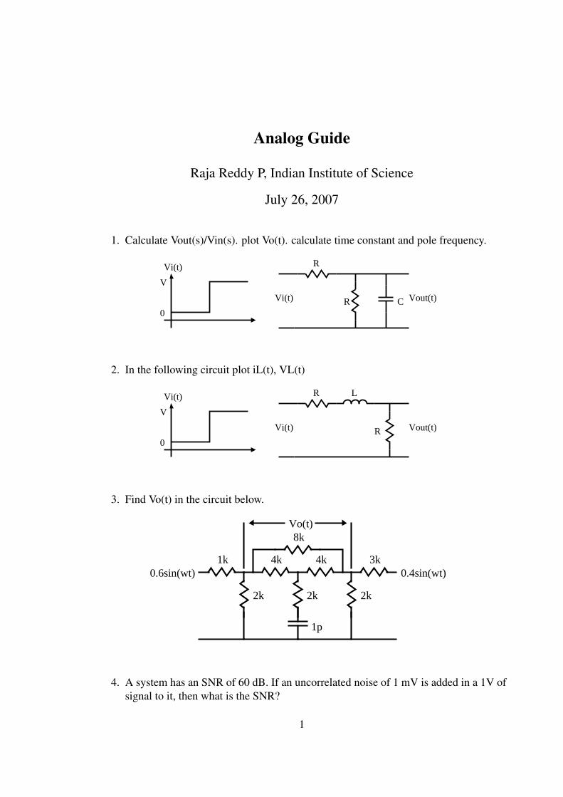
Analog Guide
Raja Reddy P, Indian Institute of Science
July 26, 2007
1. Calculate Vout(s)/Vin(s). plot Vo(t). calculate time constant and pole frequency.
R
CRVi(t) Vout(t)
0
V
Vi(t)
2. In the following circuit plot iL(t), VL(t)
0
V
Vi(t) R
Vi(t) Vout(t)R
L
3. Find Vo(t) in the circuit below.
8k
4k4k
2k
1p
2k2k
1k 3k0.4sin(wt)0.6sin(wt)
Vo(t)
4. A system has an SNR of 60 dB. If an uncorrelated noise of 1 mV is added in a 1V of
signal to it, then what is the SNR?
1
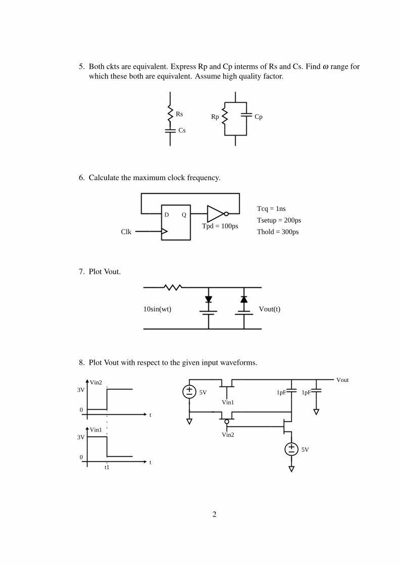
5. Both ckts are equivalent. Express Rp and Cp interms of Rs and Cs. Find ω range for
which these both are equivalent. Assume high quality factor.
Rs
Cs
Rp Cp
6. Calculate the maximum clock frequency.
D Q
ClkTpd = 100ps
Tcq = 1ns
Tsetup = 200ps
Thold = 300ps
7. Plot Vout.
10sin(wt) Vout(t)
8. Plot Vout with respect to the given input waveforms.
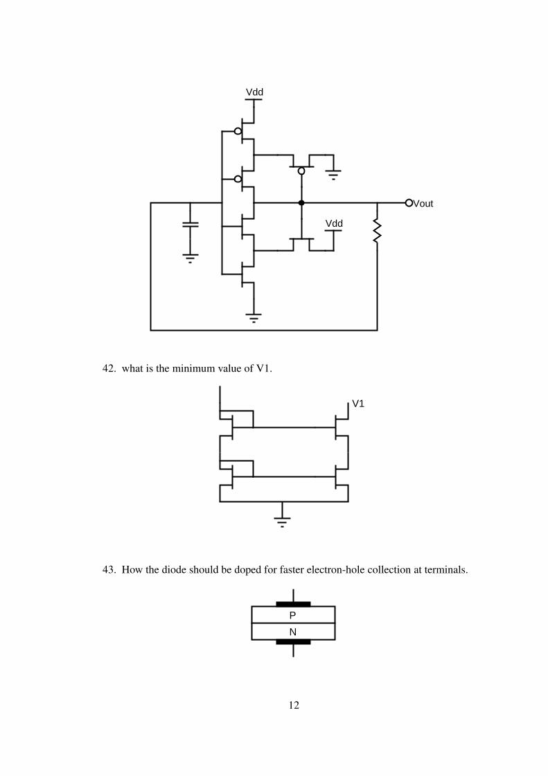
5V
5V
Vin2
1pF 1pF
Vin1
Vout
t
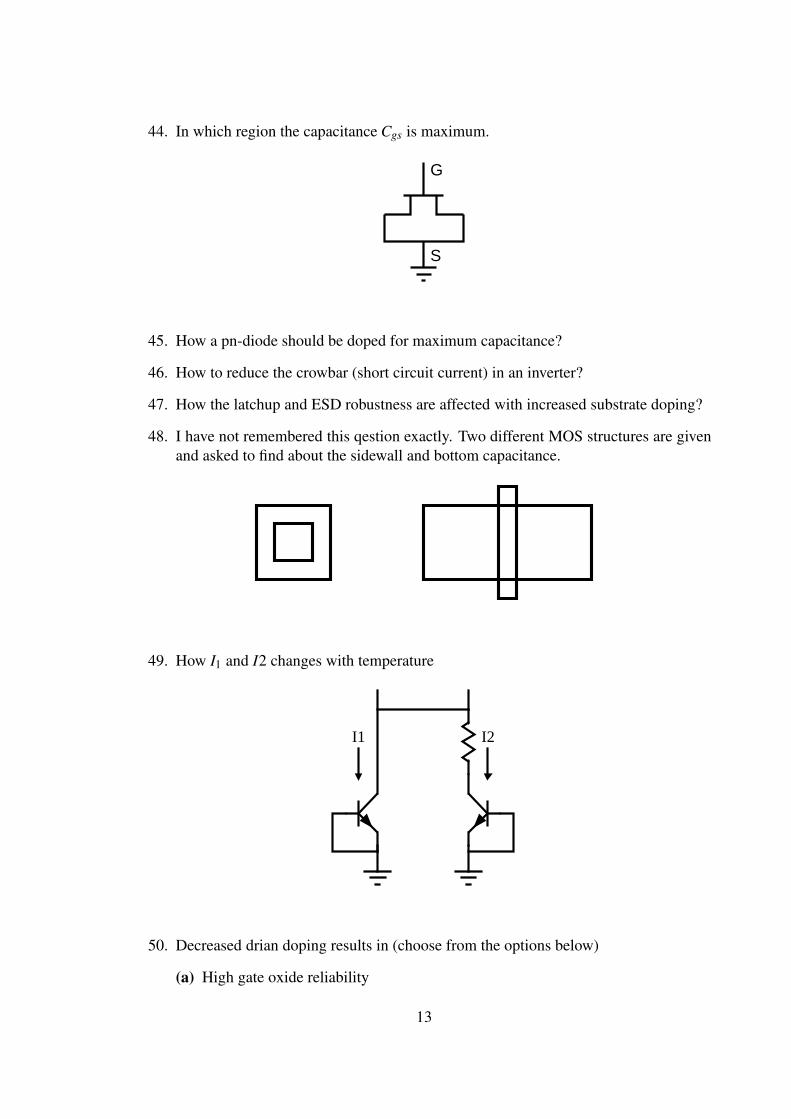
Vin2
0
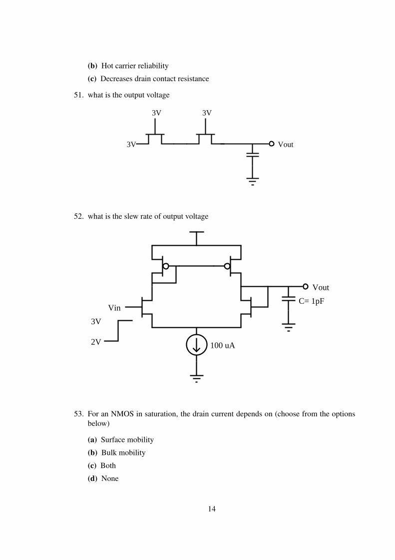
3V
t0
3VVin1
t1
2
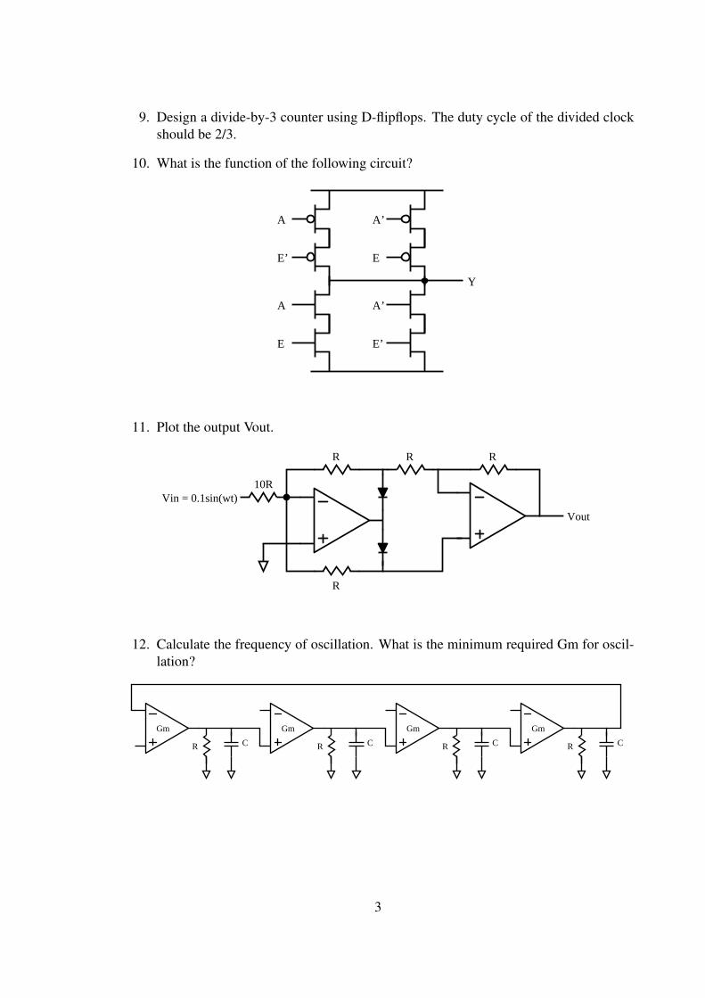
9. Design a divide-by-3 counter using D-flipflops. The duty cycle of the divided clock
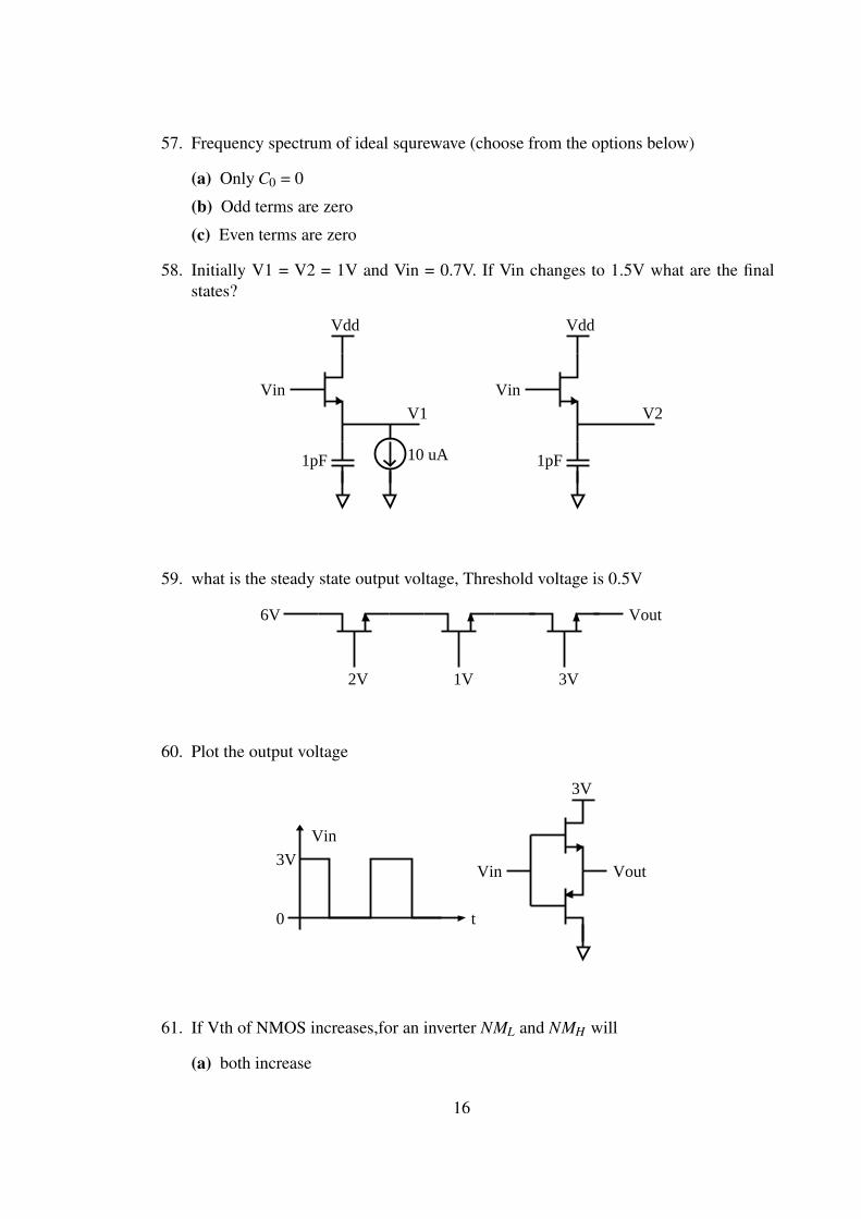
should be 2/3.
10. What is the function of the following circuit?
E
A’
E’
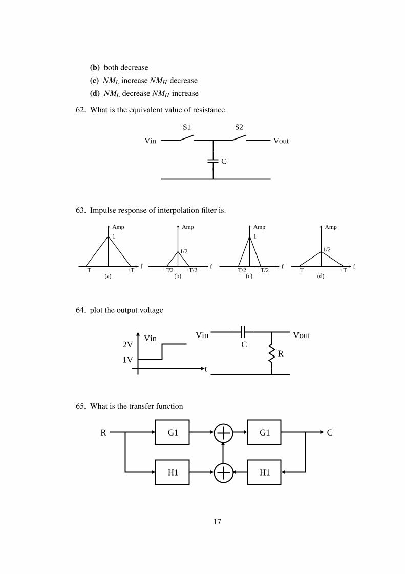
A
A
E’
A’
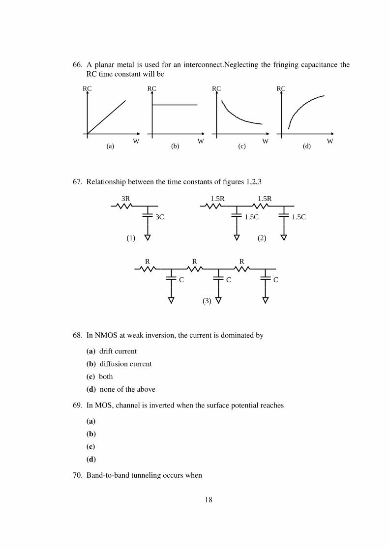
E
Y
11. Plot the output Vout.
R R R
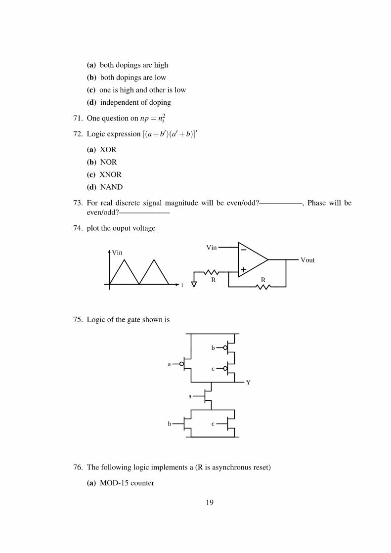
10R
R
Vin = 0.1sin(wt)
Vout
12. Calculate the frequency of oscillation. What is the minimum required Gm for oscil-
lation?
Gm
R C R R RC C C
Gm Gm Gm
3
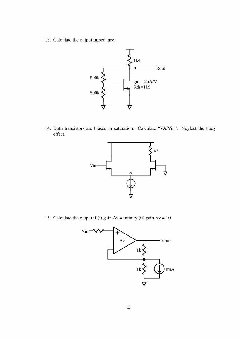
13. Calculate the output impedance.
500k
1M
500k
gm = 2uA/VRds=1M
Rout
14. Both transistors are biased in saturation. Calculate “VA/Vin”. Neglect the body
effect.
A
Rd
Vin
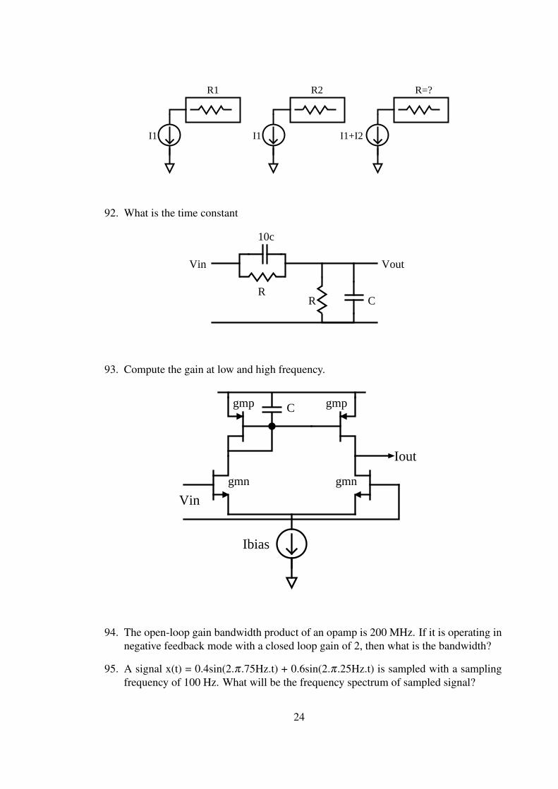
15. Calculate the output if (i) gain Av = infinity (ii) gain Av = 10
VoutAv
1k
1k 1mA
Vin
4
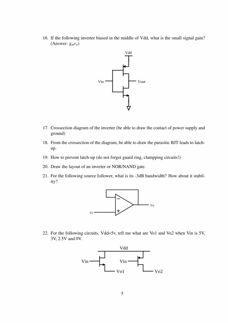
16. If the following inverter biased in the middle of Vdd, what is the small signal gain?
(Answer: gmro)
VoutVin
Vdd
17. Crossection diagram of the inverter (be able to draw the contact of power supply and
ground)
18. From the crossection of the diagram, be able to draw the parasitic BJT leads to latch-
up.
19. How to prevent latch-up (do not forget guard ring, clampping circuits!)
20. Draw the layout of an inverter or NOR/NAND gate.
21. For the following source follower, what is its -3dB bandwidth? How about it stabil-
ity?
Vi
Vo
22. For the following circuits, Vdd=5v, tell me what are Vo1 and Vo2 when Vin is 5V,
3V, 2.5V and 0V.
Vdd
VinVin
Vo1 Vo2
5
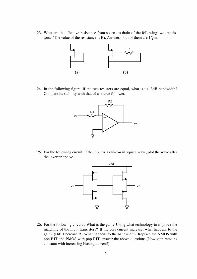
23. What are the effective resistance from source to drain of the following two transis-
tors? (The value of the resistance is R). Answer: both of them are 1/gm.
(a) (b)
R
24. In the following figure, if the two resisters are equal, what is its -3dB bandwidth?
Compare its stability with that of a source follower.
Vo
Vi
R1
R2
25. For the following circuit, if the input is a rail-to-rail square wave, plot the wave after
the inverter and vo.
Vi Vo
Vdd
26. For the following circuits, What is the gain? Using what technology to improve the
matching of the input transistors? If the bias current increase, what happens to the
gain? (Hit: Decrease!!!) What happens to the bandwidth? Replace the NMOS with
npn BJT and PMOS with pnp BJT, answer the above questions.(Now gain remains
constant with increasing biasing current!)
6
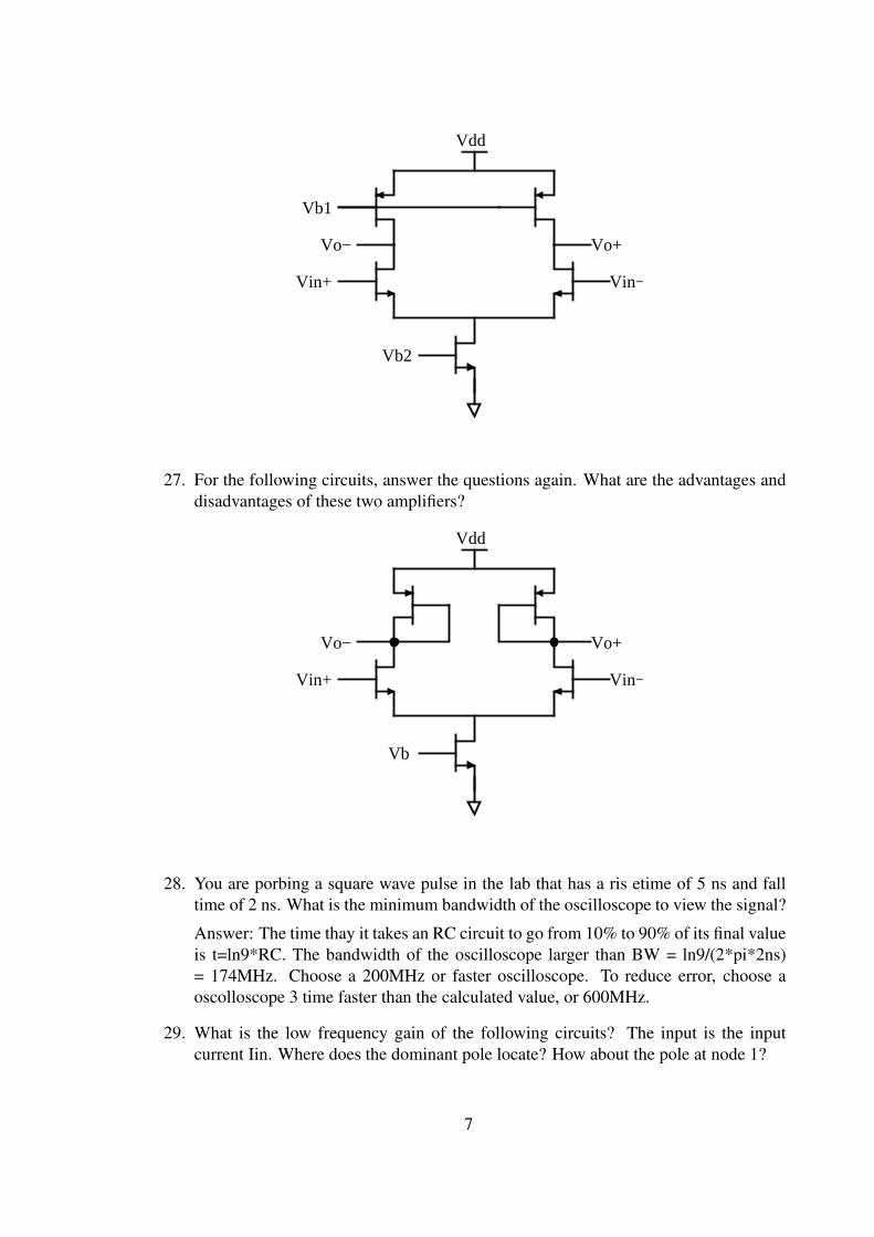
Vin+
Vo+
Vin−
Vo−
Vdd
Vb1
Vb2
27. For the following circuits, answer the questions again. What are the advantages and
disadvantages of these two amplifiers?
Vin+
Vo+
Vin−
Vo−
Vdd
Vb
28. You are porbing a square wave pulse in the lab that has a ris etime of 5 ns and fall
time of 2 ns. What is the minimum bandwidth of the oscilloscope to view the signal?
Answer: The time thay it takes an RC circuit to go from 10% to 90% of its final value
is t=ln9*RC. The bandwidth of the oscilloscope larger than BW = ln9/(2*pi*2ns)
= 174MHz. Choose a 200MHz or faster oscilloscope. To reduce error, choose a
oscolloscope 3 time faster than the calculated value, or 600MHz.
29. What is the low frequency gain of the following circuits? The input is the input
current Iin. Where does the dominant pole locate? How about the pole at node 1?
7
1Iin
Vo
R C
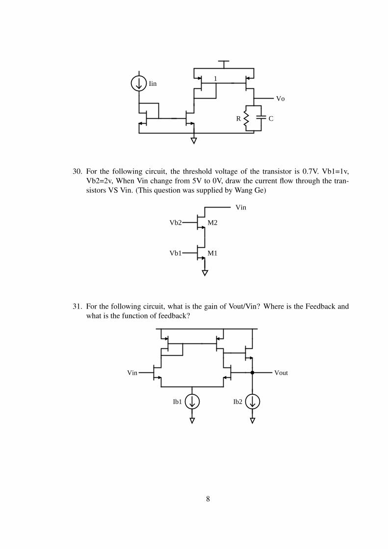
30. For the following circuit, the threshold voltage of the transistor is 0.7V. Vb1=1v,
Vb2=2v, When Vin change from 5V to 0V, draw the current flow through the tran-
sistors VS Vin. (This question was supplied by Wang Ge)
Vb1
Vb2
M1
M2
Vin
31. For the following circuit, what is the gain of Vout/Vin? Where is the Feedback and
what is the function of feedback?
Vin Vout
Ib1 Ib2
8
32. For the following circuits, the small signal input is Iin, the small signal output is vout,
what is the small signaloutput? What is the gain?
Vout
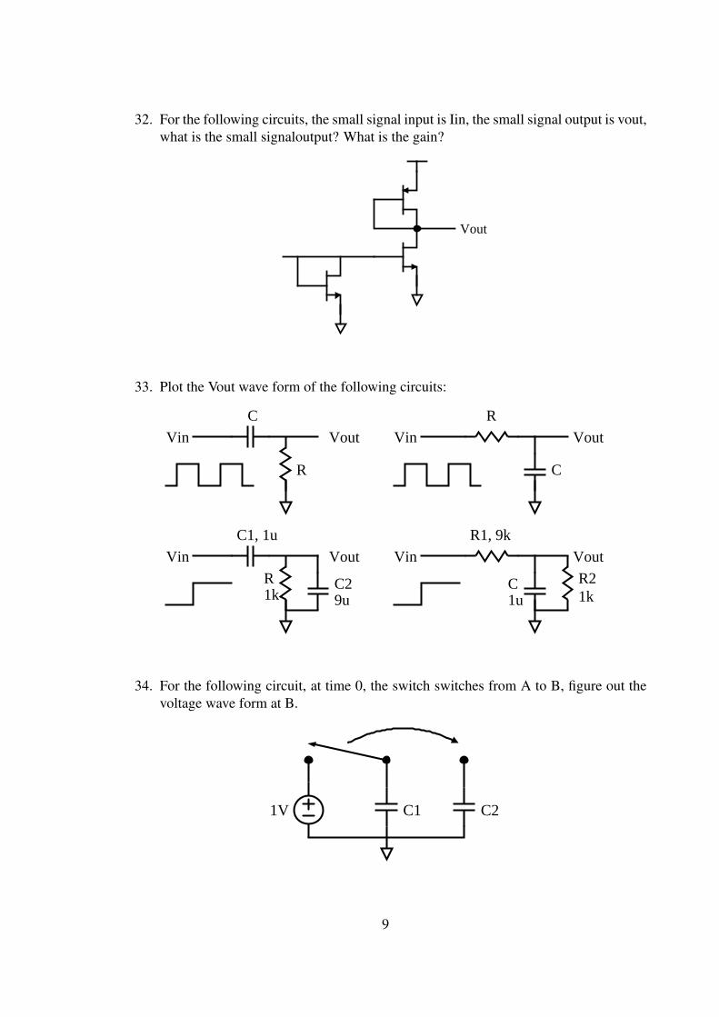
33. Plot the Vout wave form of the following circuits:
Vout
C
R
Vin
R
Vin Vout
C
VoutVin Vin Vout
9u
R1k
C1, 1u
C2
R1, 9k
R21k
C1u
34. For the following circuit, at time 0, the switch switches from A to B, figure out the
voltage wave form at B.
C2C11V
9
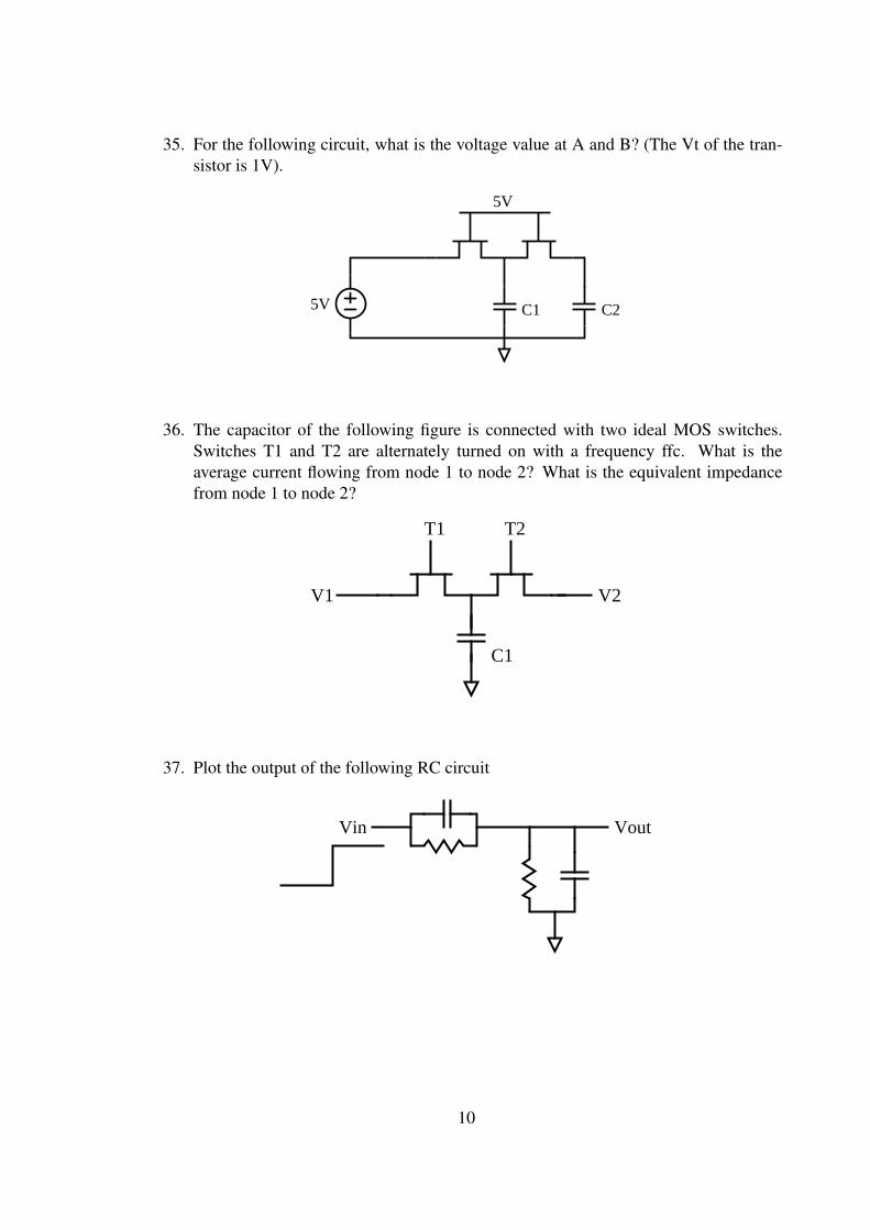
35. For the following circuit, what is the voltage value at A and B? (The Vt of the tran-
sistor is 1V).
C2C1
5V
5V
36. The capacitor of the following figure is connected with two ideal MOS switches.
Switches T1 and T2 are alternately turned on with a frequency ffc. What is the
average current flowing from node 1 to node 2? What is the equivalent impedance
from node 1 to node 2?
C1
T1 T2
V2V1
37. Plot the output of the following RC circuit
Vin Vout
10
38. How the following two circuits differ in their functionality and which one is a better
reference?
M1
M3
R
M2
M4
(a) bandgap1
R
M1
M3
M2
M4
(b) bandgap2
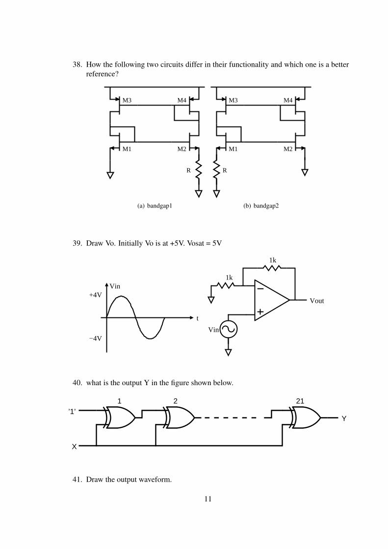
39. Draw Vo. Initially Vo is at +5V. Vosat = 5V
+4V
−4V
t
Vin
1k
1k
Vout
Vin
40. what is the output Y in the figure shown below.
’1’1 2 21
Y
X
41. Draw the output waveform.
11
Vdd
Vdd
Vout
42. what is the minimum value of V1.
V1
43. How the diode should be doped for faster electron-hole collection at terminals.
N
P
12
44. In which region the capacitance Cgs is maximum.
S
G
45. How a pn-diode should be doped for maximum capacitance?
46. How to reduce the crowbar (short circuit current) in an inverter?
47. How the latchup and ESD robustness are affected with increased substrate doping?
48. I have not remembered this qestion exactly. Two different MOS structures are given
and asked to find about the sidewall and bottom capacitance.
49. How I1 and I2 changes with temperature
I2I1
50. Decreased drian doping results in (choose from the options below)
(a) High gate oxide reliability
13
(b) Hot carrier reliability
(c) Decreases drain contact resistance
51. what is the output voltage
3V
3V 3V
Vout
52. what is the slew rate of output voltage
Vout
100 uA
C= 1pFVin
2V
3V
53. For an NMOS in saturation, the drain current depends on (choose from the options
below)
(a) Surface mobility
(b) Bulk mobility
(c) Both
(d) None
14
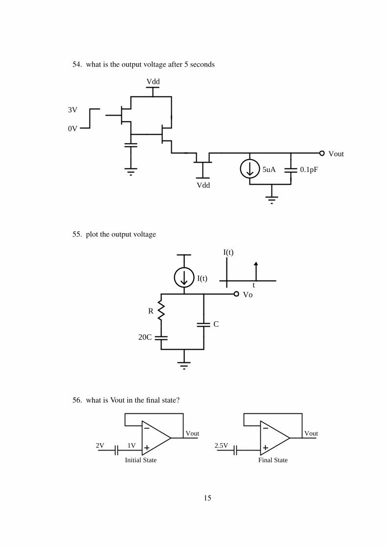
54. what is the output voltage after 5 seconds
5uA 0.1pF
3V
0V
Vdd
Vdd
Vout
55. plot the output voltage
I(t)
R
Vo
C
20C
t
I(t)
56. what is Vout in the final state?
2V 2.5V
VoutVout
Initial State Final State
1V
15
57. Frequency spectrum of ideal squrewave (choose from the options below)
(a) Only C0 = 0
(b) Odd terms are zero
(c) Even terms are zero
58. Initially V1 = V2 = 1V and Vin = 0.7V. If Vin changes to 1.5V what are the final
states?
10 uA1pF
Vin
Vdd
V1
1pF
Vin
Vdd
V2
59. what is the steady state output voltage, Threshold voltage is 0.5V
6V
2V 1V 3V
Vout
60. Plot the output voltage
3V
VoutVin
0
3V
t
Vin
61. If Vth of NMOS increases,for an inverter NML and NMH will
(a) both increase
16
(b) both decrease
(c) NML increase NMH decrease
(d) NML decrease NMH increase
62. What is the equivalent value of resistance.
S2S1
Vin Vout
C
63. Impulse response of interpolation filter is.
−T
1
Amp
f+T
(a)
Amp
f
Amp
f−T
Amp
f+T
(b) (c) (d)−T +T/2/2
1/2
1
−T/2 +T/2
1/2
64. plot the output voltage
1V
2VVin Vin
CR
t
Vout
65. What is the transfer function
G1
H1
G1
H1
R C
17
66. A planar metal is used for an interconnect.Neglecting the fringing capacitance the
RC time constant will be
W
RC
W
RC
W
RC
W
RC
(a) (d)(c)(b)
67. Relationship between the time constants of figures 1,2,3
3C
3R 1.5R 1.5R
1.5C 1.5C
R
C
R R
C C
(1) (2)
(3)
68. In NMOS at weak inversion, the current is dominated by
(a) drift current
(b) diffusion current
(c) both
(d) none of the above
69. In MOS, channel is inverted when the surface potential reaches
(a)
(b)
(c)
(d)
70. Band-to-band tunneling occurs when
18
(a) both dopings are high
(b) both dopings are low
(c) one is high and other is low
(d) independent of doping
71. One question on np = n2i
72. Logic expression [(a+b′)(a′ +b)]′
(a) XOR
(b) NOR
(c) XNOR
(d) NAND
73. For real discrete signal magnitude will be even/odd?—————–, Phase will be
even/odd?——————–
74. plot the ouput voltage
Vin
Vout
RRt
Vin
75. Logic of the gate shown is
a
b
c
a
b c
Y
76. The following logic implements a (R is asynchronus reset)
(a) MOD-15 counter
19
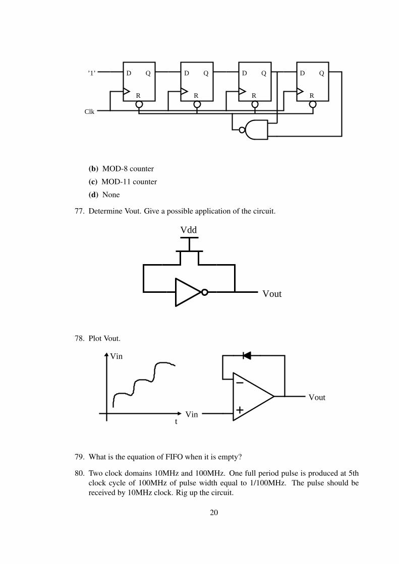
D
R
Q D
R
Q D
R
QD
R
Q’1’
Clk
(b) MOD-8 counter
(c) MOD-11 counter
(d) None
77. Determine Vout. Give a possible application of the circuit.
Vdd
Vout
78. Plot Vout.
Vout
Vin
Vin
t
79. What is the equation of FIFO when it is empty?
80. Two clock domains 10MHz and 100MHz. One full period pulse is produced at 5th
clock cycle of 100MHz of pulse width equal to 1/100MHz. The pulse should be
received by 10MHz clock. Rig up the circuit.
20
81. There is a set of 5 bits a5, a4, a3, a2, a1. Set for mod 8 counter is
(a) a1
(b) a2, a1
(c) a3, a2, a1
(d) a4, a3, a2, a1
(e) a5, a4, a3, a2, a1
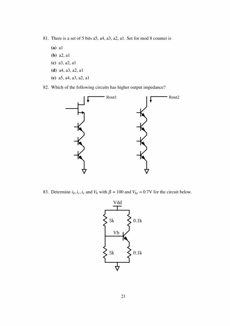
82. Which of the following circuits has higher output impedance?
Rout1 Rout2
83. Determine ib, ic, ie and Vb with β = 100 and Vbe = 0.7V for the circuit below.
5k
5k 0.1k
0.1k
Vb
Vdd
21
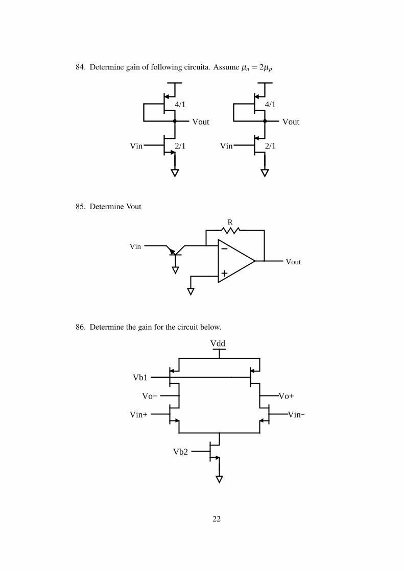
84. Determine gain of following circuita. Assume µn = 2µp
2/1
4/1
Vin
Vout
2/1
4/1
Vin
Vout
85. Determine Vout
Vout
Vin
R
86. Determine the gain for the circuit below.
Vin+
Vo+
Vin−
Vo−
Vdd
Vb1
Vb2
22
87. Frequency response for an Open loop Opamp was given and the opamp was operated
as an inverting amplifier with gain -2. Plot the closed loop frequency response.
88. Number of Boolean equation for an ’n’ input variable.
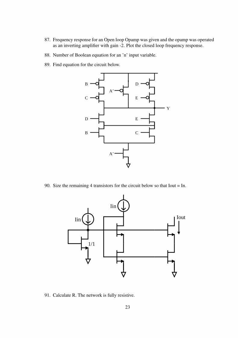
89. Find equation for the circuit below.
A’
C
ED
B
A’
B
C
D
E
Y
90. Size the remaining 4 transistors for the circuit below so that Iout = In.
Iin
Iin
Iout
1/1
91. Calculate R. The network is fully resistive.
23
R1
I1 I1
R2 R=?
I1+I2
92. What is the time constant
VoutVin
10c
RR C
93. Compute the gain at low and high frequency.
Iout
Vin
gmn gmn
gmp gmpC
Ibias
94. The open-loop gain bandwidth product of an opamp is 200 MHz. If it is operating in
negative feedback mode with a closed loop gain of 2, then what is the bandwidth?
95. A signal x(t) = 0.4sin(2.π .75Hz.t) + 0.6sin(2.π .25Hz.t) is sampled with a sampling
frequency of 100 Hz. What will be the frequency spectrum of sampled signal?
24
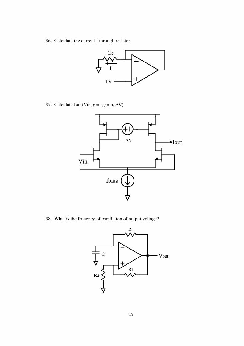
96. Calculate the current I through resistor.
1V
1k
I
97. Calculate Iout(Vin, gmn, gmp, ∆V)
Iout
Vin
Ibias
∆V
98. What is the frquency of oscillation of output voltage?
R
C
R1R2
Vout
25
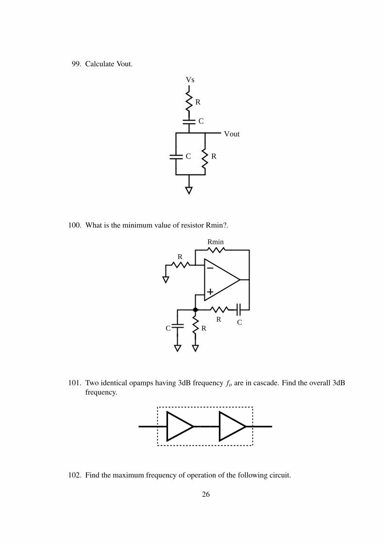
99. Calculate Vout.
R
C R
C
Vs
Vout
100. What is the minimum value of resistor Rmin?.
R CRC
R
Rmin
101. Two identical opamps having 3dB frequency fo are in cascade. Find the overall 3dB
frequency.
102. Find the maximum frequency of operation of the following circuit.
26
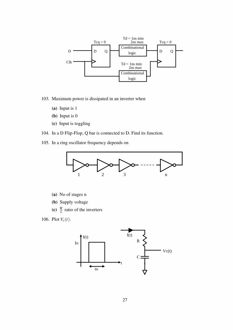
logic
Combinational
logic
Combinational
D Q D Q
Td = 1ns min 2ns max
2ns maxTd = 1ns min
Tcq = 0 Tcq = 0
D
Clk
103. Maximum power is dissipated in an inverter when
(a) Input is 1
(b) Input is 0
(c) Input is toggling
104. In a D Flip-Flop, Q bar is connected to D. Find its function.
105. In a ring oscillator frequency depends on
1 2 3 n
(a) No of stages n
(b) Supply voltage
(c) WL
ratio of the inverters
106. Plot Vc(t).
Vc(t)
C
RI(t)
Io
to
t
I(t)
27
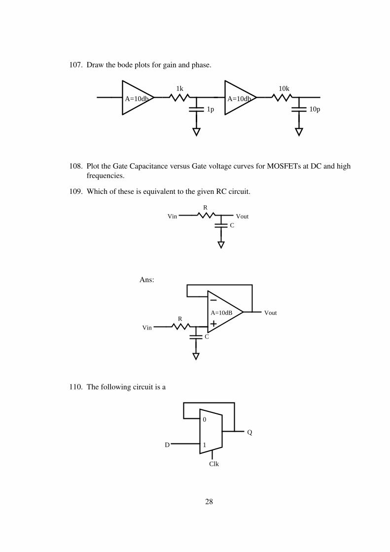
107. Draw the bode plots for gain and phase.
1k
A=10db
10k
1p 10p
A=10db
108. Plot the Gate Capacitance versus Gate voltage curves for MOSFETs at DC and high
frequencies.
109. Which of these is equivalent to the given RC circuit.
R
C
Vin Vout
R
C
Vin
VoutA=10dB
Ans:
110. The following circuit is a
0
1D
Clk
Q
28
(a) level 0 transparent latch
(b) level 1 transparent latch
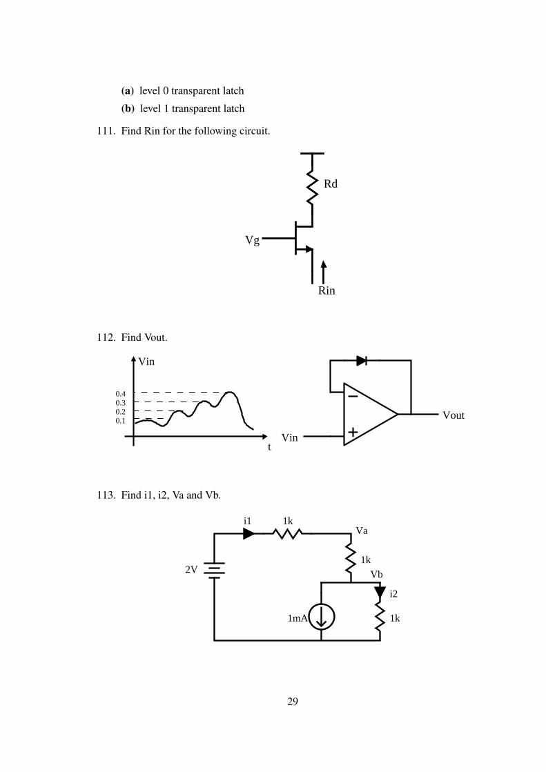
111. Find Rin for the following circuit.
Vg
Rd
Rin
112. Find Vout.
Vout
Vint
Vin
0.20.30.4
0.1
113. Find i1, i2, Va and Vb.
2V
1k
1k
Va
1mA 1k
i2
Vb
i1
29
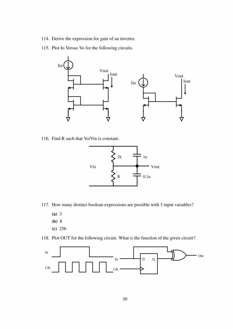
114. Derive the expression for gain of an inverter.
115. Plot Io Versus Vo for the following circuits.
Iin
IoutVout
Iin
VoutIout
116. Find R such that Vo/Vin is constant.
Vin Vout
1k 1u
R 0.1u
117. How many distinct boolean expressions are possible with 3 input variables?
(a) 3
(b) 8
(c) 256
118. Plot OUT for the following circuit. What is the function of the given circuit?
D Q
In
Clk
In
Clk
Out
30