Embed Size (px)
Citation preview

ANALOG ELECTRONICS
1. In a voltage-voltage feedback as shown below, which one of the following statements is TRUE if
the gain k is increased?
(A) The input impedance increases and output impedance decreases
(B) The input impedance increases and output impedance also increases
(C) The input impedance decreases and output impedance also decreases
(D) The input impedance decreases and output impedance increases.
2. In the circuit shown below the op-amps are ideal. Then, Vout in Volts is
(A) 4 (B) 6 (C) 8 (D) 10
3. In the circuit shown below what is the output voltage Vout if a silicon transistor Q and an ideal op-amp
are used?

(A) -15 V (B) -0.7 V (C) +0.7 V (D) +15 V
4. The circuit shown is a
(A) Low pass filter with f3db=1/(R1+R2)C radians/s
(B) High pass filter with f3db=1/R1C radians/s
(C) Low pass filter with f3db=1/R1C radians/s
(D) High pass filter with f3db=1/(R1+R2)C radians/s.
5. The circuit below implements a filter between the input current ii and the output voltage vo . Assume
that the op-amp is ideal. The filter implemented is a
(A) Low pass filter (B) Band pass filter (C) Band stop filter (D) High pass filter
6. Assuming the OP-AMP to be ideal, the voltage gain of the amplifier shown below is

(A) –R2/R1 (B)-R3/R1 (C)-(R2||R3)/R1 (D) -(R2+R3)/R1
7. The transfer characteristic for the precision rectifier circuit shown below is (assume ideal OP-AMP and
practical diodes)
Ans: B
8. In the following a stable multivibrator circuit, which properties of Vo(t) depend on R2?

(A) Only the frequency (B) Only the amplitude (C) Both the amplitude and the frequency (D)
Neither the amplitude nor the frequency
9. In the circuit shown below, the op-amp is ideal, the transistor has VBE = 0 6. V and b = 150. Decide
whether the feedback in the circuit is positive or negative and determine the voltage V at the output of
the op-amp.
(A) Positive feedback, V = 10 V (B) Positive feedback, V = 0 V (C) Negative feedback, V = 5 V (D)
Negative feedback, V = 2 V
10. The OPAMP circuit shown above represents a
(A) High pass filter (B) Low pass filter (C) Band pass filter (D) Band reject filter.
11. Consider the Schmidt trigger circuit shown below A triangular wave which goes from -12 to 12 V is
applied to the inverting input of OPMAP. Assume that the output of the OPAMP swings from +15 V to -
15 V. The voltage at the non-inverting input switches between

(A) -12V to +12 V (B) -7.5 V to 7.5 V (C) -5 V to +5 V (D) 0 V and 5 V
12. In the Op-Amp circuit shown, assume that the diode current follows the equation I =Is exp(V/VT ) .
For Vi = 2V,V0= V01 and for Vi = 4V,V0= V02. The relationship between V01 and V02 is
(A)V02=(2)1/2V01 (B)V02=(e)2V01 (C) V02=V011n2 (D) V01-V02 =VT1n2
Statement for Linked Answer Question 13& 14 :
Consider the Op-Amp circuit shown in the figure.
13. The transfer function V0(S)/vI(S) is
(A)1-sRC/1+sRC (B)1+sRC/1-sRC (c)1/1-sRC (d)1/1+sRC
14. If Vi= V1sin(wt) and V0= V2sin( wt+φ) , then the minimum and maximum values of φ (in radians) are
respectively
(A)- /2 and /2 p (B) 0 and /2(C) - and 0 (D) /2 and 0
15. The voltage e0 is indicated in the figure has been measured by an ideal voltmeter. Which of the
following can be calculated?

(A) Bias current of the inverting input only (B) Bias current of the inverting and non-inverting inputs
only(C) Input offset current only (D) Both the bias currents and the input offset current.
16. The Op-amp circuit shown in the figure is filter. The type of filter and its cut. Off frequency are
respectively
(A) High pass, 1000 rad/sec. (B) Low pass, 1000 rad/sec (C) High pass, 1000 rad/sec (D) Low pass,
10000 rad/sec
17. Given the ideal operational amplifier circuit shown in the figure indicate the correct transfer
characteristics assuming ideal diodes with zero cut-in voltage.

Ans: B
18. An ideal op-amp is an ideal
(A) Voltage controlled current source (B) Voltage controlled voltage source (C) Current controlled
current source (D) Current controlled voltage source
19. The circuit in the figure is a
(A) Low-pass filter (B) High-pass filter (C) Band-pass filter (D) Band-reject filter
20. The value of C required for sinusoidal oscillations of frequency 1 kHz in the circuit of the figure is

(A) 1/2πµF(B) 2πµF (C)1/2π (6)1/2µF (D) 2π (6)1/2µF
21. In the op-amp circuit given in the figure, the load current iL is
(A)-Vs/R2(B) Vs/R2(C)-Vs/RL (D) Vs/R1
22. If the input to the ideal comparators shown in the figure is a sinusoidal signal of 8 V (peak to peak)
without any DC component, then the output of the comparators has a duty cycle of
(A) 1/2 (B) 1/3 (C) 1/6 (D) ½
23. If the differential voltage gain and the common mode voltage gain of a differential amplifier are 48
dB and 2 dB respectively, then common mode rejection ratio is
(A) 23 dB (B) 25 dB (C) 46 dB (D) 50 dB
24. Generally, the gain of a transistor amplifier falls at high frequencies due to the
(A) Internal capacitances of the device (B) Coupling capacitor at the input (C) Skin effect (D) Coupling
capacitor at the output

25. An amplifier without feedback has a voltage gain of 50, input resistance of 1 k W and output
resistance of 2.5 kW. The input resistance of the current-shunt negative feedback amplifier using the
above amplifier with a feedback factor of 0.2, is
(A)1/11 KΩ (B) 1/5 KΩ (C) 5 KΩ (D) 11 KΩ
26. In the amplifier circuit shown in the figure, the values of R1 and R2 are such that the transistor is
operating at VCE = 3 V and IC = 1 5. mA when its β is 150. For a transistor with β of 200, the operating
point ( VCE,IC) is
(A) (2 V, 2 mA) (B) (3 V, 2 mA) (C) (4 V, 2 mA) (D) (4 V, 1 mA)
27. The oscillator circuit shown in the figure has an ideal inverting amplifier. Its frequency of oscillation
(in Hz) is
(A)1/2πRC(6)1/2 (B )1/2πRC (C) 1/RC(6)1/2 (D) (6)1/2 /2πRC
28. The output voltage of the regulated power supply shown in the figure is
(A) 3 V (B) 6 V (C) 9 V (D) 12 V
29. If the op-amp in the figure is ideal, the output voltage Vout will be equal to

(A) 1 V (B) 6 V (C) 14 V (D) 17 V
30. Three identical amplifiers with each one having a voltage gain of 50, input resistance of 1 kΩ and
output resistance of 250 Ω are cascaded. The opened circuit voltages gain of the combined amplifier is
(A) 49 dB (B) 51 dB (C) 98 dB (D) 102 dB
31. An ideal saw-tooth voltages waveform of frequency of 500 Hz and amplitude 3 V is generated by
charging a capacitor of 2 mF in every cycle. The charging requires
(A) Constant voltage source of 3 V for 1 ms (B) Constant voltage source of 3 V for 2 ms (C) Constant
voltage source of 1 mA for 1 ms(D) Constant voltage source of 3 mA for 2 ms
Statement for Linked Answer Question 32 &33 :
In the following transistor circuit, VBE = 0 7. V, r3 = 25 mV/IE , and b and all the capacitances are very
large
32. The value of DC current IE is
(A) 1 mA (B) 2 mA (C) 5 mA (D) 10 mA
33. The mid-band voltage gain of the amplifier is approximately
(A) -180 (B) -120 (C) -90 (D) -60
34. For the Op-Amp circuit shown in the figure, V0 is

(A) -2 V (B) -1 V (C) -0.5 V (D) 0.5 V
35. For the BJT circuit shown, assume that the βof the transistor is very large and VBE = 0.7 V.
The mode of operation of the BJT is
(A) cut-off (B) saturation (C) normal active (D) reverse active
36. The input impedance (Zi) and the output impedance (Z0) of an ideal trans-conductance
(voltage controlled current source) amplifier are
(A) Zi= 0,Z0= 0 (B) Zi= 0,Z0 = 3 (C) Zi= 3,Z0 = 0 (D) Zi= 3,Z0 = 3 37. For the circuit shown in the following figure, the capacitor C is initially uncharged. At t = 0
the switch S is closed. The Vc across the capacitor at t = 1 millisecond is
In the figure shown above, the OP-AMP is supplied with +/-15V
(A) 0 Volt (B) 6.3 Volt (C) 9.45 Volts (D) 10 Volts.
38. In an ideal differential amplifier shown in the figure, a large value of (RE).
(A) Increase both the differential and common - mode gains.
(B) Increases the common mode gain only.
(C) Decreases the differential mode gain only.
(D) Decreases the common mode gain only. 39. The cascade amplifier is a multistage configuration of
(A) CC - CB (B) CE - CB
(C) CB - CC (D) CE – CC
40. The effect of current shunt feedback in an amplifier is to
(A) Increase the input resistance and decrease the output resistance
(B) Increases both input and output resistance
(C) Decrease both input and output resistance
(D) Decrease the input resistance and increase the output resistance
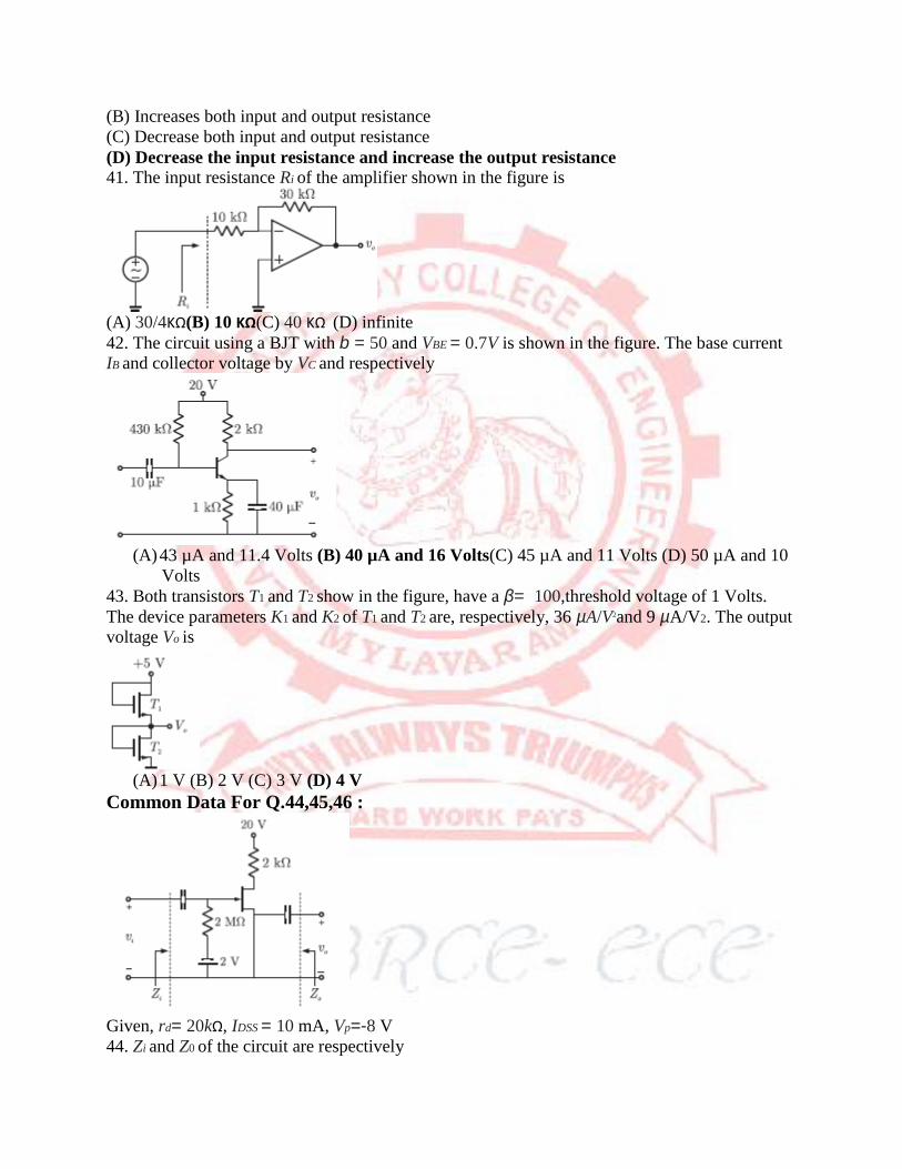
41. The input resistance Ri of the amplifier shown in the figure is
(A) 30/4KΩ(B) 10 KΩ(C) 40 KΩ (D) infinite
42. The circuit using a BJT with b = 50 and VBE = 0.7V is shown in the figure. The base current
IB and collector voltage by VC and respectively
(A) 43 µA and 11.4 Volts (B) 40 µA and 16 Volts(C) 45 µA and 11 Volts (D) 50 µA and 10
Volts
43. Both transistors T1 and T2 show in the figure, have a β= 100,threshold voltage of 1 Volts.
The device parameters K1 and K2 of T1 and T2 are, respectively, 36 µA/V2and 9 µA/V2. The output
voltage Vo is
(A) 1 V (B) 2 V (C) 3 V (D) 4 V
Common Data For Q.44,45,46 :
Given, rd= 20kΩ, IDSS = 10 mA, Vp=-8 V
44. Zi and Z0 of the circuit are respectively

(A) 2 MΩ and 2 kΩ(B) 2 MΩ and 20/11 kΩ (C) infinity and 2 MΩ(D) infinity and 20/11KΩ
45.ID and VDS under DC conditions are respectively
(A) 5.625 mA and 8.75 V (B) 1.875 mA and 5.00 V
(C) 4.500 mA and 11.00 V (D) 6.250 mA and 7.50 V
46. Transconductance in milli-Siemens (mS) and voltage gain of the amplifier are respectively
(A) 1.875 mS and 3.41 (B) 1.875 ms and -3.41(C) 3.3 mS and -6 (D) 3.3 mS and 6
Common Data For Q. 47 & 48: A regulated power supply, shown in figure below, has an unregulated input (UR) of 15 Volts and
generates a regulated output Vout. Use the component values shown in the figure.
47. The power dissipation across the transistor Q1 shown in the figure is
(A) 4.8 Watts (B) 5.0 Watts (C) 5.4 Watts (D) 6.0 Watts
48. If the unregulated voltage increases by 20%, the power dissipation across the transistor Q1
(A) Increases by 20% (B) Increases by 50% (C) Remains unchanged (D) Decreases by 20%
49. A bipolar transistor is operating in the active region with a collector current of 1 mA.
Assuming that the β of the transistor is 100 and the thermal voltage (VT) is 25 mV, the
Transconductance (gm) and the input resistance (r ) of the transistor in the common emitter
configuration, are
(A) gm= 25 mA/V and r = 15.625 kW
(B) gm= 40 mA/V and r = 4.0 kW
(C) gm= 25 mA/V and r = 2.5 k W
(D) gm= 40 mA/V and r = 2.5 kW 50. Assume that the βof transistor is extremely large and VBE = 0.7V, ICand VCE in the circuit
shown in the figure
(A) IC = 1mA,VCE= 4.7 V (B) IC = 0.5 mA, VCE = 3.75 V
(C) IC = 1 mA, VCE = 2.5 V (D) IC = 0.5 mA, VCE = 3.9 V
51. Choose the correct match for input resistance of various amplifier configurations shown
below:
Configuration Input resistance

CB : Common Base LO : Low
CC : Common Collector MO : Moderate
CE : Common Emitter HI : High
(A) CB - LO, CC -MO, CE - HI
(B) CB - LO, CC - HI, CE -MO
(C) CB -MO, CC - HI, CE - LO
(D) CB - HI, CC - LO, CE –MO
52. A 741-type op-amp has a gain-bandwidth product of 1 MHz. A non-inverting amplifier suing
this op-amp and having a voltage gain of 20 dB will exhibit a -3 dB bandwidth of
(A) 50kHz (B) 100kHz (C) 1000/17kHz (D) 1000/7.07kHz
53. Three identical RC-coupled transistor amplifiers are cascaded. If each of the amplifiers has a
frequency response as shown in the figure, the overall frequency response is as given in
Ans: A
54. An amplifier using an op amp with a slew-rate SR = 1 V/µ sec has a gain of 40 dB. If this
amplifier has to faithfully amplify sinusoidal signals from dc to 20 kHz without introducing any
slew-rate induced distortion, then the input signal level must not exceed.
(A) 795 mV (B) 395 mV (C) 79.5 mV (D) 39.5 mV
55. The oscillator circuit shown in the figure is

(A) Hartely oscillator with foscillation= 79.6 MHz
(B) Colpitts oscillator with foscillation= 50.3 MHz
(C) Hartley oscillator with foscillation= 159.2 MHz
(D) Colpitts oscillator with foscillation= 159.3 MHz
56. Three ideal OP-AMP has the following characteristics.
(A) Ri= ∞, A = ∞,R0= 0(B) Ri= 0, A = ∞, R0 = 0 (C) Ri= ∞, A = ∞, R0 =∞(D) Ri= 0, A = ∞, R0
=∞ 57. Consider the following two statements:
Statement 1: A stable multi vibrator can be used for generating square wave.
Statement 2: Bistable multi vibrator can be used for storing binary information.
(A) Only statement 1 is correct
(B) Only statement 2 is correct
(C) Both the statements 1 and 2 are correct
(D) Both the statements 1 and 2 are incorrect
58. An npn BJT has gm = 38 mA/V, Cµ= 10-14
F,Cπ= 4*10-16
and DC current gain β0 = 90. For this
transistor fT and fb are
(A) fT=1.64 *108Hz and fβ=1.47 *10
10Hz (B)fT =1.47 *10
10Hz and fβ=1.64 *10
8Hz
(C) fT =1.33 *1012
Hz and fβ=1.47 *1010
Hz (D)fT =1.47 *1010
Hz and fβ=1.33 *1012
Hz
59.The transistor shunt regulator shown in the figure has a regulated output voltage of 10 V,
when the input varies from 20 V to 30 V.The relevant parameters for the zener diode and the
transistor are: Vz= 9.5, VBE = 0.3 V, β = 99, Neglect the current through RB. Then the maximum
power dissipated in the zener diode (Pz) and the transistor (PT) is
(A) Pz= 75 mW, PT = 7.9 W
(B) Pz= 85 mW, PT = 8.9 W
(C) Pz= 95 mW, PT = 9.9 W
(D) Pz= 115 mW, PT = 11.9 W
60.The inverting OP-AMP shown in the figure has an open-loop gain of 100

The closed-loop gain V0/Vsis
(A) -8 (B) -9 (C) -10 (D) -11
61. In the differential amplifier of the figure, if the source resistance of the current source IEE is
infinite, then the common-mode gain is
(A) zero (B) Infinite (C) Indeterminate (D)Vin1+Vin2/2VT
62. Introducing a resistor in the emitter of a common amplifier stabilizes the dc operating point
against variations in
(A) Only the temperature (B) Only the β of the transistor
(C) Both temperature and β (D) None of the above
63. The current gain of a bipolar transistor drops at high frequencies because of
(A) Transistor capacitances
(B) High current effects in the base
(C) Parasitic inductive elements
(D) The Early effect
64. If the op-amp in the figure, is ideal, then v0 is
(A) Zero
(B) (V1- V2) sinwt
(C) -(V1+ V2) sinwt (D) (V1+ V2) sinwt
65. The most commonly used amplifier is sample and hold circuits is
(A) A unity gain inverting amplifier
(B) A unity gain non-inverting amplifier

(C) An inverting amplifier with a gain of 10
(D) An inverting amplifier with a gain of 100
66. In the circuit of figure, assume that the transistor is in the active region. It has a large β and
its base-emitter voltage is 0.7 V. The value of Icis
(A) Indeterminate since Rcis not given (B) 1 mA (C) 5 mA (D) 10 mA
67. The first dominant pole encountered in the frequency response of a compensated op-amp is
approximately at
(A) 5Hz (B) 10 kHz (C) 1MHz (D) 100 MHz
68. Negative feedback in an amplifier
(A) Reduces gain
(B) Increases frequency and phase distortions
(C) Reduces bandwidth
(D) Increases noise
69.In the cascade amplifier shown in the given figure, if the commonemitter stage (Q1) has a
transconductancegm1, and the common base stage (Q2) has a transconductancegm2, then the
overall Transconductance g(= i0 /vi) of the cascade amplifier is
(A) gm1(B) gm2 (C) gm1/2(D) gm2/2
70. Crossover distortion behavior is characteristic of
(A) Class A output stage (B) Class B output stage
(C) Class AB output stage (D) Common-base output stage
71. An amplifier has an open-loop gain of 100, an input impedance of 1 kΩ,and an output
impedance of 100 Ω. A feedback network with a feedback factor of 0.99 is connected to the
amplifier in a voltage series feedback mode. The new input and output impedances, respectively,
are
(A) 10 Ω and 1Ω (B) 10 Ω and 10 kΩ (C) 100 kΩ and 1Ω (D) 100 kΩ and 1 kΩ 72. The circuit of the figure is an example of feedback of the following type

(A) Current series (B) Current shunt (C) Voltage series (D) Voltage shunt
73. In a differential amplifier, CMRR can be improved by using an increased
(A) Emitter resistance (B) Collector resistance (C) Power supply voltages (D) Source resistance
74. From a measurement of the rise time of the output pulse of an amplifier whose is a small
amplitude square wave, one can estimate the following parameter of the amplifier
(A) Gain-bandwidth product (B) Slew rate (C) Upper 3–dB frequency (D) Lower 3–dB
frequency
75.The emitter coupled pair of BJT’s given a linear transfer relation between the differential
output voltage and the differential output voltage and the differential input voltage Vid is less α times the thermal voltage, where α is
(A) 4 (B) 3(C) 2 (D) 1
76. In a shunt-shunt negative feedback amplifier, as compared to the basic amplifier
(A) Both, input and output impedances, decrease
(B) Input impedance decreases but output impedance increases
(C) Input impedance increase but output
(D) Both input and output impedances increases
77. A multistage amplifier has a low-pass response with three real poles at s =-w1- w2 and w3.
The approximate overall bandwidth B of the amplifier will be given by
(A) B = w1+ w2+ w3(B) 1/B=1/w1+1/w2+1/w3 (C) )B =(w1+ w2+ w3 )1/8
(D)
B=(W12+W2
2+W3
2)1/2
78. A cascade amplifier stags is equivalent to
(A) A common emitter stage followed by a common base stage
(B) A common base stage followed by an emitter follower
(C) An emitter follower stage followed by a common base stage
(D) A common base stage followed by a common emitter stage
79. In a common emitter BJT amplifier, the maximum usable supply voltage is limited by
(A) Avalanche breakdown of Base-Emitter junction
(B) Collector-Base breakdown voltage with emitter open (BVCBO)
(C) Collector-Emitter breakdown voltage with base open (BVCBO)
(D) Zener breakdown voltage of the Emitter-Base junction
80. For small signal ac operation, a practical forward biased diode can be modelled as
(A) A resistance and a capacitance in series
(B) An ideal diode and resistance in parallel
(C) A resistance and an ideal diode in series
(D) A resistance
81. In a negative feedback amplifier using voltage-series (i.e. voltage sampling, series mixing) feedback. (A) Ri decreases and R0 decreases (B) Ri decreases and R0 increases (C) Ri increases and R0 decreases (D) Ri increases and R0 increases (Ri and R0 denote the input and output resistance respectively) 82. In the BJT amplifier shown in the figure is the transistor is based in the forward active region. Putting a capacitor across RE will

(A) Decrease the voltage gain and decrease the input impedance (B) Increase the voltage gain and decrease the input impedance (C) Decrease the voltage gain and increase the input impedance (D)Increase the voltage gain and increase the input impedance 83. The circuit shown in the figure is that of
(A) A non-inverting amplifier (B) An inverting amplifier (C) An oscillator (D) A Schmitt trigger
84. In the circuit shown in the given figure N is a finite gain amplifier with a gain of k , a very large input impedance, and a very low output impedance. The input impedance of the feedback amplifier with the feedback impedance Z connected as shown will be
(A) Z(1-1/k)(B) Z(1-k)(C) Z/(k-1) (D)Z/(1-k)
85. A Darlington stage is shown in the figure. If the transconductance of Q1 is gm1 and Q2 is gm2, then the overall Transconductance gmc is given by
(A) gm1(B) 0 5. gm1(C) gm2 (D) 0 5. gm2

86. The ac schematic of an NMOS common-source state is shown in the figure below, where part of the biasing circuits has been omitted for simplicity. For the n-channel MOSFET M, the transconductance gm = 1 / mA V, and body effect and channel length modulation effect are to be neglected. The lower cutoff frequency in HZ of the circuit is approximately
(A) 8 (B) 32 (C) 50 (D) 200 87. In the circuit shown below, the silicon npn transistor Q has a very high value of β. The required value of R2 in kΩ to produce IC = 1 mA is
(A) 20 (B) 30 (C) 40 (D) 50 88. The current ib through the base of a silicon npn transistor is 1+0.1 cos(10000πt)mA at 300 K, the rπin the small signal model of the transistor is
(A) 250 Ω (B) 27.5 Ω(C) 25 Ω (D) 22.5Ω
89. The impedance looking into nodes 1 and 2 in the given circuit is

(A) 50 Ω(B) 100 Ω (C) 5 kΩ (D) 10.1 kΩ 90.The voltage gain Av of the circuit shown below is
(A) Av ≈200 (B) Av≈100 (C) Av≈20 (D) Av≈10
91. In the circuit shown below, capacitors C1 and C2 are very large and are shorts at the input frequency. vi is a small signal input. The gain magnitude |Vo/vi| at 10 M rad/s is
(A) Maximum(B) Minimum (C) Unity (D) Zero 92. In the circuit shown below, for the MOS transistors, µnCox=100µA/v2and the threshold voltage VT = 1 V. The voltage Vx at the source of the upper transistor is
(A) 1 V (B) 2 V (C) 3 V (D) 3.67 V
93. For the BJT, Q1 in the circuit shown below,β=∞ , V BEon =0.7, V CEsat=0.7. The switch is initially closed. At time t = 0, the switch is opened. The time t at which Q1 leaves the active region is

(A) 10 ms (B) 25 ms (C) 50 ms (D) 100 ms
94. For a BJT, the common base current gain α = 0.98 and the collector base junction reverse bias saturation current ICO =0.6 µA . This BJT is connected in the common emitter mode and operated in the active region with a base drive current IB=20µA . The collector current IC for this mode of operation is (A) 0.98 mA (B) 0.99 mA (C) 1.0 mA (D) 1.01 mA Common Data For Q. 95 &96 : Consider the common emitter amplifier shown below with the following circuit parameters: β=100,gm=0.3861 A/V,r0=259Ω,Rs=1KΩ,RB =93KΩ,Rc=250KΩ,RL =1KΩ,C1 =∞,C2 =4.7µF
95. The resistance seen by the source vS is (A) 258 Ω(B) 1258 Ω (C) 93 kΩ (D) ∞ 96. The lower cut-off frequency due to C2 is (A) 33.9 Hz (B) 27.1 Hz (C) 13.6 Hz (D) 16.9 Hz 97. The amplifier circuit shown below uses a silicon transistor. The capacitors CC and CE can be assumed to be short at signal frequency and effect of output resistance r0 can be ignored. If CE is disconnected from the circuit, which one of the following statements is true

(A) The input resistance Ri increases and magnitude of voltage gainAV decreases (B) The input resistance Ri decreases and magnitude of voltage gain AV increases (C) Both input resistance Ri and magnitude of voltage gain AV decreases (D) Both input resistance Ri and the magnitude of voltage gain AV increases 98. In the silicon BJT circuit shown below, assume that the emitter area of transistor Q1 is half that of transistor Q2
The value of current Io is approximately (A) 0.5 mA (B) 2 mA (C) 9.3 mA (D) 15 mA Statement for Linked Answer Question 99 & 100: Consider for CMOS circuit shown, where the gate voltage v0 of the n-MOSFET is increased from zero, while the gate voltage of the p -MOSFET is kept constant at 3 V. Assume, that, for both transistors, the magnitude of the threshold voltage is 1 V and the product of the trans-conductance parameter is 1mA. V
99. For small increase in VG beyond 1V, which of the following gives the correct description of the region of operation of each MOSFET? (A) Both the MOSFETs are in saturation region (B) Both the MOSFETs are in triode region (C) n-MOSFETs is in triode and p -MOSFET is in saturation region

(D) n- MOSFET is in saturation and p -MOSFET is in triode region 100. Estimate the output voltage V0 for VG = 1 5. V. (A) 4-1/√2 (B)4+1/√2 (C)4-√3/2 (D) 4+√3/2 101. A small signal source Vi(t )=A cos 20t+B sin 106t is applied to a transistor amplifier as shown below. The transistor has β = 150 and hie=3Ω.Which expression best approximate V 0t .
(A)V 0(t )= -1500( A cos 20t+B sin 106t ) (B)V 0(t )= -1500( A cos 20t+B sin 106t) (C)V 0(t )= -1500( B sin 106t) (D) V 0(t )= -150( B sin 106t) 102. For the circuit shown in the following figure, transistor M1 and M2 are identical NMOS transistors. Assume the M2 is in saturation and the output is unloaded.
The current Ix is related to Ibias as (A)Ix= Ibias+ Is (B)Ix= Ibias (C)Ix= Ibias-(VDD-VOT/RE) (D)Ix= Ibias- Is 103. Two identical NMOS transistors M1 and M2 are connected as shown below. Vbias is chosen so that both transistors are in saturation. The equivalent gm of the pair is defied to be ∂IOUT/∂Vi at constant VoutThe equivalent gm of the pair is
(A) The sum of individual gm 's of the transistors (B) The product of individual gm’s of the transistors

(C) Nearly equal to the gm of M1 (D) Nearly equal to gm/g 0 of M2
Common Data For Q. 104,105 & 106: In the transistor amplifier circuit shown in the figure below, the transistor has the following parameters: βDC = 60, VBE = 0 7V,hie→∞ The capacitance CC can be assumed to be infinite.
104. Under the DC conditions, the collector-or-emitter voltage drop is (A) 4.8 Volts (B) 5.3 Volts (C) 6.0 Volts (D) 6.6 Volts 105. If βDC is increased by 10%, the collector-to-emitter voltage drop (A) Increases by less than or equal to 10% (B) Decreases by less than or equal to 10% (C) Increase by more than 10% (D) Decreases by more than 10% 106. One input terminal of high gain comparator circuit is connected to ground and a sinusoidal voltage is applied to the other input. The output of comparator will be (A) a sinusoid (B) a full rectified sinusoid (C) a half rectified sinusoid (D) a square wave 107. In the BJT amplifier shown in the figure is the transistor is based in the forward active region. Putting a capacitor across RE will
(A) Decrease the voltage gain and decrease the input impedance (B) Increase the voltage gain and decrease the input impedance (C) Decrease the voltage gain and increase the input impedance (D) Increase the voltage gain and increase the input impedance 108. The number of comparators required in a 3-bit comparators type ADC (A) 2 (B) 3 (C) 7 (D) 8 109. An 8 bit successive approximation analog to digital communication has full scale reading of 2.55 V and its conversion time for an analog input of 1 V is 20 µs. The conversion time for a 2 V input will be (A) 10 µs (B) 20 µs (C) 40 µs (D) 50 µs. 110. The number of comparator in a 4-bit flash ADC is

(A) 4 (B) 5 (C) 15 (D) 16 111. For the 4 bit DAC shown in the figure, the output voltage V0 is
(A) 10 V (B) 5 V (C) 4 V (D) 8 V
112. The resolution of a 4-bit counting ADC is 0.5 volts. For an analog input of 6.6 volts, the digital output of the ADC will be (A) 1011 (B) 1101 (C) 1100 (D) 1110 113. The advantage of using a dual slope ADC in a digital voltmeter is that (A) Its conversion time is small (B) Its accuracy is high (C) It gives output in BCD format (D) It does not require a 114. The current I through resistance r in the circuit shown in the figure is
(A) –V/12R (B) V /12R (C) V/ 6R (D)V/3 T
115. A 12-bit ADC is operating with a 1 m sec clock period and the total conversion time is seen to be 14 m sec. The ADC must be of the (A) Flash type (B) Counting type (C) Intergrating type (D) Successive approximation type 116. A cascade connection of two voltage amplifiers A1 and A2 is shown in the figure. The openloop gain
Av0, input resistance Rin, and output resistance RO for A1 and A2 are as follows:
A1 :Av0 =10, Rin =10kΩ, RO =1kΩ
A2 :Av0 =5, Rin =5kΩ, RO =200Ω
The approximate overall voltage gain Vout / Vin is ______________

Answer: 34.722
117. For the n-channel MOS transistor shown in the figure, the threshold voltage VTh is 0.8 V. Neglect
channel length modulation effects. When the drain voltage VD = 1.6 V, the drain current ID was found
to be 0.5 mA. If VD is adjusted to be 2 V by changing the values of R and VDD, the new value of ID (in
mA) is
(A) 0.625 (B) 0.75 (C) 1.125 (D) 1.5
Answer: (C)
118. For the MOSFETs shown in the figure, the threshold voltage|Vt|=2V and K=1/2
µCoX(W/L)=0.1mA/V2.The value of ID (in mA) is ________.
Answer: 0.9
119. The following signal Vi of peak voltage 8V is applied to the non-inverting terminal of an ideal op-
amp. The transistor has V BE=0.7V, β=100;V VLED=1.5V,VCC= 10Vand- VCC=- 1V.

The number of times the LED glows_____________
Ans: 3
120. Consider the oscillator circuit shown in the figure. The function of the network (shown in dotted
lines) consisting of the 100kΩ resistor in series with the two diodes connected back-to back is to:
(A) Introduce amplitude stabilization by preventing the op amp from saturating and thus producing
sinusoidal oscillations of fixed amplitude
(B) Introduce amplitude stabilization by forcing the op-amp to swing between positive and negative
saturation and thus producing square wave oscillations of fixed amplitude

(C) Introduce frequency stabilization by forcing the circuit to oscillate at a single frequency
(D) Enable the loop gain to take on a value that produces square wave oscillations
Ans: A
121. The block diagram of a frequency synthesizer consisting of a Phase Locked Loop (PLL) and a
divide-by-𝑁 counter (comprising 2, 4, 8, 16 outputs) is sketched below. The synthesizer is
excited with a 5 kHz signal (Input 1). The free-running frequency of the PLL is set to20 kHz. Assume
that the commutator switch makes contacts repeatedly in the order 1-2-3-4.
The corresponding frequencies synthesized are:
(A) 10 kHz, 20 kHz, 40 kHz, 80 kHz
(B) 20 kHz, 40 kHz, 80 kHz, 160 kHz
(C) 80 kHz, 40 kHz, 20 kHz, 10 kHz
(D) 160 kHz, 80 kHz, 40 kHz, 20 kHz
122. Which one of the following statements is correct about an ac-coupled common-emitter amplifier
operating in the mid-band region?
(A) The device parasitic capacitances behave like open circuits, whereas coupling and by pass
capacitances behave like short circuits.
(B) The device parasitic capacitances, coupling capacitances and bypass capacitances behave like open
circuits.
(C) The device parasitic capacitances, coupling capacitances and bypass capacitances behave like short
circuits.
(D) The device parasitic capacitances behave like short circuits, whereas coupling and bypass
capacitances behave like open circuits.
Ans: A

123. In the op-amp circuit shown, the Zener diodesZ1 and Z2 clamp the output voltage V0 to +5 V or−5
V. The switch S is initially closed and is opened at time 𝑡= 0.
The time t = t1(in seconds) at which V0changes state is__________
Ans: 0.789
124. An op-amp has a finite open loop voltage gain of 100. Its input offset voltage Vios(=+5mV) is
modeled as shown in the circuit below. The amplifier is ideal in all other respects. Vinput is 25mV
The output voltage (in millivolts) is ___________.
Ans: 413.79
125. In an N bit flash ADC, the analog voltage is fed simultaneously to 2N − 1 comparators. The outputof
the comparators is then encoded to a binary format using digital circuits. Assume that the analog
voltage source Vin(whose output is being converted to digital format) has a source resistance of 75 as
shown in the circuit diagram below and the input capacitance of each comparator is 8 pF. The input
must settle to an accuracy of 1/2LSB even for a full scale input change for proper conversion. Assume
that the time taken by the thermometer to binary encoder is negligible.

If the flash ADC has 8 bit resolution, which one of the following alternatives is closest to the maximum
sampling rate?
(A) 1 megasamples per second
(B) 6 megasamples per second
(C) 64 megasamples per second
(D) 256 megasamples per second
Ans: A
126. Consider the circuit shown in the figure. Assuming VBE1 = VEB2 = 0.7 volt, the value of the dc
voltage VC2 (in volt) is
Ans: 0.5
127. In the astable multivibrator circuit shown in the figure, the frequency of oscillation (in kHz) at the
output pin 3 is__________________

Ans: 5.64.
128. In the circuit shown in the figure, transistor M1 is in saturation and has transconductance gm =
0.01 siemens. Ignoring internal parasitic capacitances and assuming the channel length modulation to
be zero, the small signal input pole frequency (in kHz) is_____________
Key: 57.
129. A 10-bit ADC with a full scale output voltage of 10.24 V is designed to have a ±LSB/2 accuracy. If the
ADC is calibrated at 250C and the operating temperature ranges from 00 to 250C, then the maximum net
temperature coefficient of the ADC should not exceed
(A) ±200 µV /0C(B )±400 µV /0C (C) ±600 µV /0C (D) ±800 µV /0C

130. A non-inverting op-amp has got a gain of 10. The open-loop gain of the op-amp is 2*10
5. Its output
resistance is 75. Calculate the output resistance of the non-inverting amplifier. 131. Design an op-amp waveform generating circuit to produce the waveform given in figure below. Explain the circuit operation with other relevant waveform.
132. Design a Schmitt trigger circuit using an op-amp which has a maximum output voltage of 10 V . The ‘hysteresis’ – VH should be = 0.4V. Explain the working of the circuit with the transfer characteristics. Use of reference voltage VR = 2V. 133. With a block diagram, explain the function of a dual slope DVM. 134. A dual slope integrating type of A/D converter has an integrating capacitor 0.1µF and a resistance of
100k. The reference voltage is 2 V and the output of the integrator is not to exceed 10V. What is the maximum time required for the output voltage to be integrated? 135. Define and deduce an expression for the slew rate of an op-amp. A particular op-amp has a slew rate of 0.5 V / µs . It is used as a non-inverting amplifier with a gain of 25. The voltage gain against frequency curve is fat up to 50 kHz. Calculate the maximum peak to-peak input signal that can be applied to get the undistorted output.
136. Match List I (Circuit) with List II (Property) and select the correct answer : List I A. R-C coupled single-stage amplifier B. Emitter follower C. Common base amplifier D. Darlington amplifier List II 1. Beta multiplier 2. Constant current source 3. Very high input impedance 4. Phase inverter with voltage gain A B C D a. 3 4 1 2 b. 4 3 1 2 c. 3 4 2 1 d. 4 3 2 1 137. Consider the following statements in respect of a transistor R-C coupled amplifier : 1. The low frequency response is determined by the transistor junction capacitors 2. The high frequency response is limited by coupling capacitors. 3. The Miller capacitance reduces the gain at high frequencies. 4. As the gain is increased the bandwidth gets reduced. Which of these statements are correct? a. 1 and 2 b. 2 and 3 c. 3 and 4 d. 1 and 4

138. In a BJT amplifier with the introduction of feedback, the input impedance is reduced, output impedance is increased, bandwidth is increased and distortion is reduced. The feedback is a. Voltage series b. Current series c. Voltage shunt d. Current shunt 139. An amplifier has two identical cascaded stages. Each stage has a bandwidth of 20kHz. The overall bandwidth shall approximately be equal to a. 10 kHz b. 12.9 kHz c. 20 kHz d. 28.3 kHz 140. The common emitter current gain-bandwidth product of a transistor (fT) is defined as the frequency at which a. Alpha of the transistor falls by 3 dB b. Beta of the transistor falls by 3 dB c. Beta of the transistor falls to unity d. Power gain of the transistor falls to unity 9 141. Which of the following components control the low frequency of the R-C coupled amplifier? 1. Wiring capacitance 2. Parasitic capacitances of transistor 3. Coupling capacitances 4. Emitter bypass capacitance 142. Assertion (A) : If the emitter bypass capacitor of an R-C coupled, CE amplifier gets disconnected, its voltage gain increases. Reason (R) : The un bypassed emitter resistor gives negative feedback. a. Both A and R are individually true and R is the correct explanation of A b. Both A and R are individually true but R is not the correct explanation of A c. A is true but R is false d. A is false but R is true 143. Assertion (A) : A self- biased BJT circuit is more stable as compared to a fixed biased one Reason (R) : A self-biased BJT circuit uses more components as compared to a fixed biased one. a. Both A and R are individually true and R is the correct explanation of A b. Both A and R are individually true but R is not the correct explanation of A c. A is true but R is false d. A is false but R is true 10 144. Assertion (A) : Wien bridge oscillator is generally used as a variable audio frequency oscillator. Reason (R) : By varying either the capacitor or resistor value in one arms of the bridge, the frequency of the Wien bridge oscillator can be varied. a. Both A and R are individually true and R is the correct explanation of A b. Both A and R are individually true but R is not the correct explanation of A c. A is true but R is false d. A is false but R is true 145. Assertion (A) : A linear, negative feedback control system is invariably stable if its open loop configuration is stable. Reason (R) : The negative feedback reduces the overall gain of the system. a. Both A and R are individually true and R is the correct explanation of A b. Both A and R are individually true but R is not the correct explanation of A c. A is true but R is false d. A is false but R is true


![[eBook] LabView - Engineering Fundamentals of Digital Electronics.pdf](https://img.pdfslide.us/doc/110x75/55cf9998550346d0339e30ae/ebook-labview-engineering-fundamentals-of-digital-electronicspdf.jpg)