Embed Size (px)
Citation preview
Analog Drawing Board
6.101 Final Project Report Henry Love & Nicholas Klugman
Spring 2017
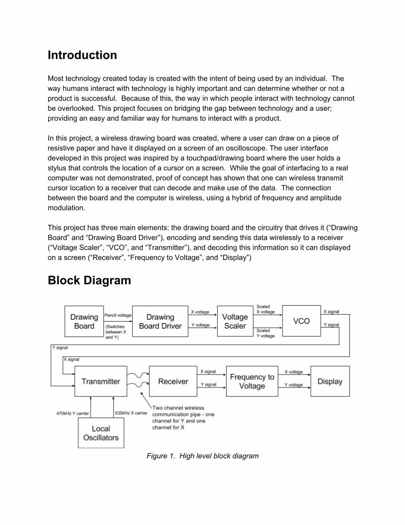
Introduction Most technology created today is created with the intent of being used by an individual. The way humans interact with technology is highly important and can determine whether or not a product is successful. Because of this, the way in which people interact with technology cannot be overlooked. This project focuses on bridging the gap between technology and a user; providing an easy and familiar way for humans to interact with a product. In this project, a wireless drawing board was created, where a user can draw on a piece of resistive paper and have it displayed on a screen of an oscilloscope. The user interface developed in this project was inspired by a touchpad/drawing board where the user holds a stylus that controls the location of a cursor on a screen. While the goal of interfacing to a real computer was not demonstrated, proof of concept has shown that one can wireless transmit cursor location to a receiver that can decode and make use of the data. The connection between the board and the computer is wireless, using a hybrid of frequency and amplitude modulation. This project has three main elements: the drawing board and the circuitry that drives it (“Drawing Board” and “Drawing Board Driver”), encoding and sending this data wirelessly to a receiver (“Voltage Scaler”, “VCO”, and “Transmitter”), and decoding this information so it can displayed on a screen (“Receiver”, “Frequency to Voltage”, and “Display”)
Block Diagram
Figure 1. High level block diagram
A note on signals between modules in the block diagram: A “voltage” label corresponds to a voltage level being transmitted between modules. A “signal” label corresponds to a sine wave (in voltage) being transmitted between modules. A wavy arrow (such as the one between “Transmitter” and “Receiver”) corresponds to an AM waveform between modules.
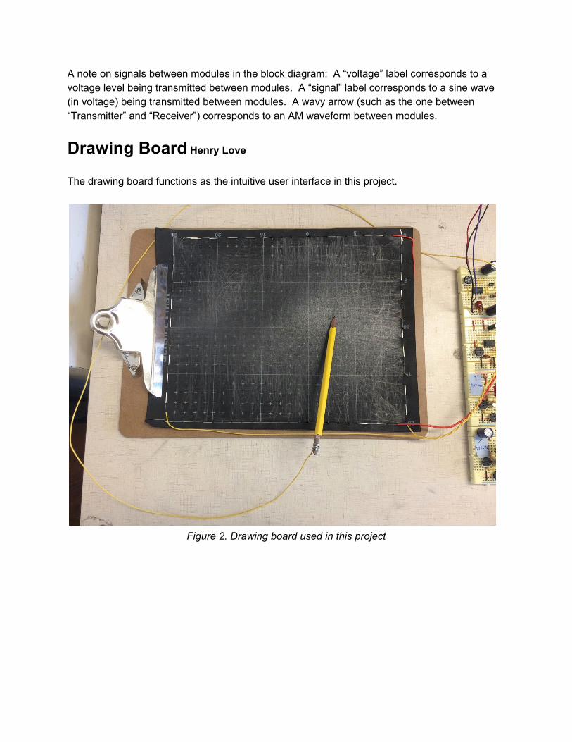
Drawing Board Henry Love The drawing board functions as the intuitive user interface in this project.
Figure 2. Drawing board used in this project
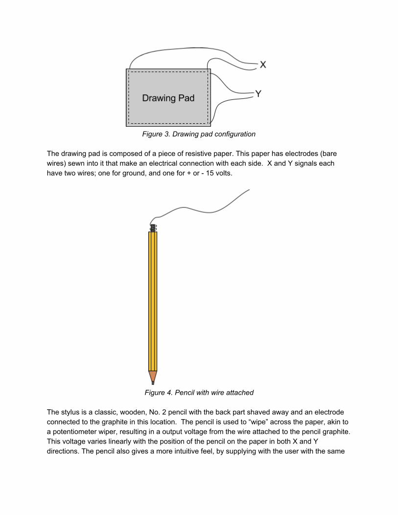
Figure 3. Drawing pad configuration
The drawing pad is composed of a piece of resistive paper. This paper has electrodes (bare wires) sewn into it that make an electrical connection with each side. X and Y signals each have two wires; one for ground, and one for + or - 15 volts.
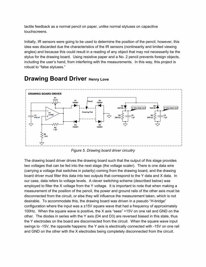
Figure 4. Pencil with wire attached
The stylus is a classic, wooden, No. 2 pencil with the back part shaved away and an electrode connected to the graphite in this location. The pencil is used to “wipe” across the paper, akin to a potentiometer wiper, resulting in a output voltage from the wire attached to the pencil graphite. This voltage varies linearly with the position of the pencil on the paper in both X and Y directions. The pencil also gives a more intuitive feel, by supplying with the user with the same
tactile feedback as a normal pencil on paper, unlike normal styluses on capacitive touchscreens. Initially, IR sensors were going to be used to determine the position of the pencil, however, this idea was discarded due the characteristics of the IR sensors (nonlinearity and limited viewing angles) and because this could result in a reading of any object that may not necessarily be the stylus for the drawing board. Using resistive paper and a No. 2 pencil prevents foreign objects, including the user’s hand, from interfering with the measurements. In this way, this project is robust to “false styluses.”
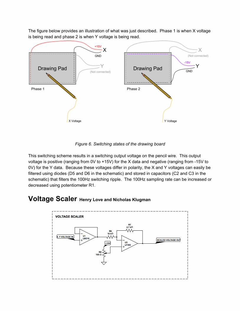
Drawing Board Driver Henry Love
Figure 5. Drawing board driver circuitry
The drawing board driver drives the drawing board such that the output of this stage provides two voltages that can be fed into the next stage (the voltage scaler). There is one data wire (carrying a voltage that switches in polarity) coming from the drawing board, and the drawing board driver must filter this data into two outputs that correspond to the Y data and X data. In our case, data refers to voltage levels. A clever switching scheme (described below) was employed to filter the X voltage from the Y voltage. It is important to note that when making a measurement of the position of the pencil, the power and ground rails of the other axis must be disconnected from the circuit, or else they will influence the measurement taken, which is not desirable. To accommodate this, the drawing board was driven in a pseudo “H-bridge” configuration where the input was a ±15V square wave that had a frequency of approximately 100Hz. When the square wave is positive, the X axis “sees” +15V on one rail and GND on the other. The diodes in series with the Y axis (D4 and D3) are reversed biased in this state, thus the Y electrodes on the board are disconnected from the circuit. When the square wave input swings to -15V, the opposite happens: the Y axis is electrically connected with -15V on one rail and GND on the other with the X electrodes being completely disconnected from the circuit.
The figure below provides an illustration of what was just described. Phase 1 is when X voltage is being read and phase 2 is when Y voltage is being read.
Figure 6. Switching states of the drawing board
This switching scheme results in a switching output voltage on the pencil wire. This output voltage is positive (ranging from 0V to +15V) for the X data and negative (ranging from -15V to 0V) for the Y data. Because these voltages differ in polarity, the X and Y voltages can easily be filtered using diodes (D5 and D6 in the schematic) and stored in capacitors (C2 and C3 in the schematic) that filters the 100Hz switching ripple. The 100Hz sampling rate can be increased or decreased using potentiometer R1.
Voltage Scaler Henry Love and Nicholas Klugman
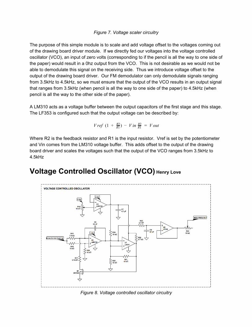
Figure 7. Voltage scaler circuitry
The purpose of this simple module is to scale and add voltage offset to the voltages coming out of the drawing board driver module. If we directly fed our voltages into the voltage controlled oscillator (VCO), an input of zero volts (corresponding to if the pencil is all the way to one side of the paper) would result in a 0hz output from the VCO. This is not desirable as we would not be able to demodulate this signal on the receiving side. Thus we introduce voltage offset to the output of the drawing board driver. Our FM demodulator can only demodulate signals ranging from 3.5kHz to 4.5kHz, so we must ensure that the output of the VCO results in an output signal that ranges from 3.5kHz (when pencil is all the way to one side of the paper) to 4.5kHz (when pencil is all the way to the other side of the paper). A LM310 acts as a voltage buffer between the output capacitors of the first stage and this stage. The LF353 is configured such that the output voltage can be described by:
(1 ) V in V outV ref + R1R2 − R1
R2 =
Where R2 is the feedback resistor and R1 is the input resistor. Vref is set by the potentiometer and Vin comes from the LM310 voltage buffer. This adds offset to the output of the drawing board driver and scales the voltages such that the output of the VCO ranges from 3.5kHz to 4.5kHz
Voltage Controlled Oscillator (VCO) Henry Love
Figure 8. Voltage controlled oscillator circuitry
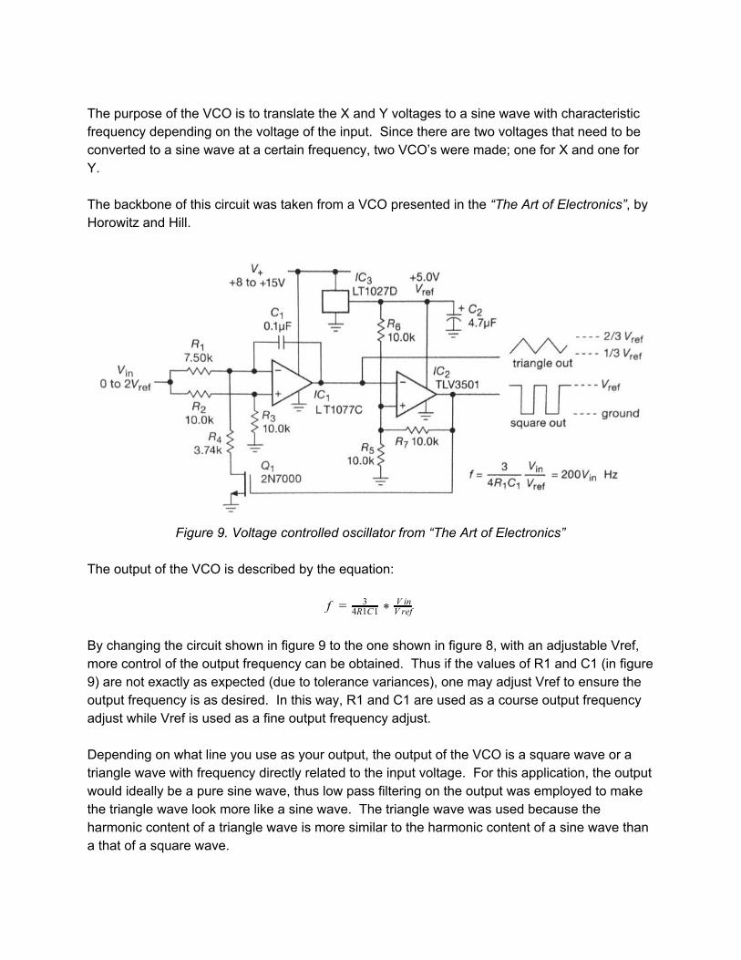
The purpose of the VCO is to translate the X and Y voltages to a sine wave with characteristic frequency depending on the voltage of the input. Since there are two voltages that need to be converted to a sine wave at a certain frequency, two VCO’s were made; one for X and one for Y. The backbone of this circuit was taken from a VCO presented in the “The Art of Electronics”, by Horowitz and Hill.
Figure 9. Voltage controlled oscillator from “The Art of Electronics”
The output of the VCO is described by the equation:
f = 34R1C1 * V in
V ref By changing the circuit shown in figure 9 to the one shown in figure 8, with an adjustable Vref, more control of the output frequency can be obtained. Thus if the values of R1 and C1 (in figure 9) are not exactly as expected (due to tolerance variances), one may adjust Vref to ensure the output frequency is as desired. In this way, R1 and C1 are used as a course output frequency adjust while Vref is used as a fine output frequency adjust. Depending on what line you use as your output, the output of the VCO is a square wave or a triangle wave with frequency directly related to the input voltage. For this application, the output would ideally be a pure sine wave, thus low pass filtering on the output was employed to make the triangle wave look more like a sine wave. The triangle wave was used because the harmonic content of a triangle wave is more similar to the harmonic content of a sine wave than a that of a square wave.
Local Oscillators Henry Love
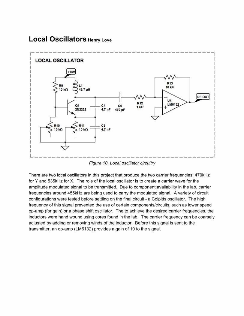
Figure 10. Local oscillator circuitry
There are two local oscillators in this project that produce the two carrier frequencies: 470kHz for Y and 535kHz for X. The role of the local oscillator is to create a carrier wave for the amplitude modulated signal to be transmitted. Due to component availability in the lab, carrier frequencies around 455kHz are being used to carry the modulated signal. A variety of circuit configurations were tested before settling on the final circuit - a Colpitts oscillator. The high frequency of this signal prevented the use of certain components/circuits, such as lower speed op-amp (for gain) or a phase shift oscillator. The to achieve the desired carrier frequencies, the inductors were hand wound using cores found in the lab. The carrier frequency can be coarsely adjusted by adding or removing winds of the inductor. Before this signal is sent to the transmitter, an op-amp (LM6132) provides a gain of 10 to the signal.
Transmitter Henry Love
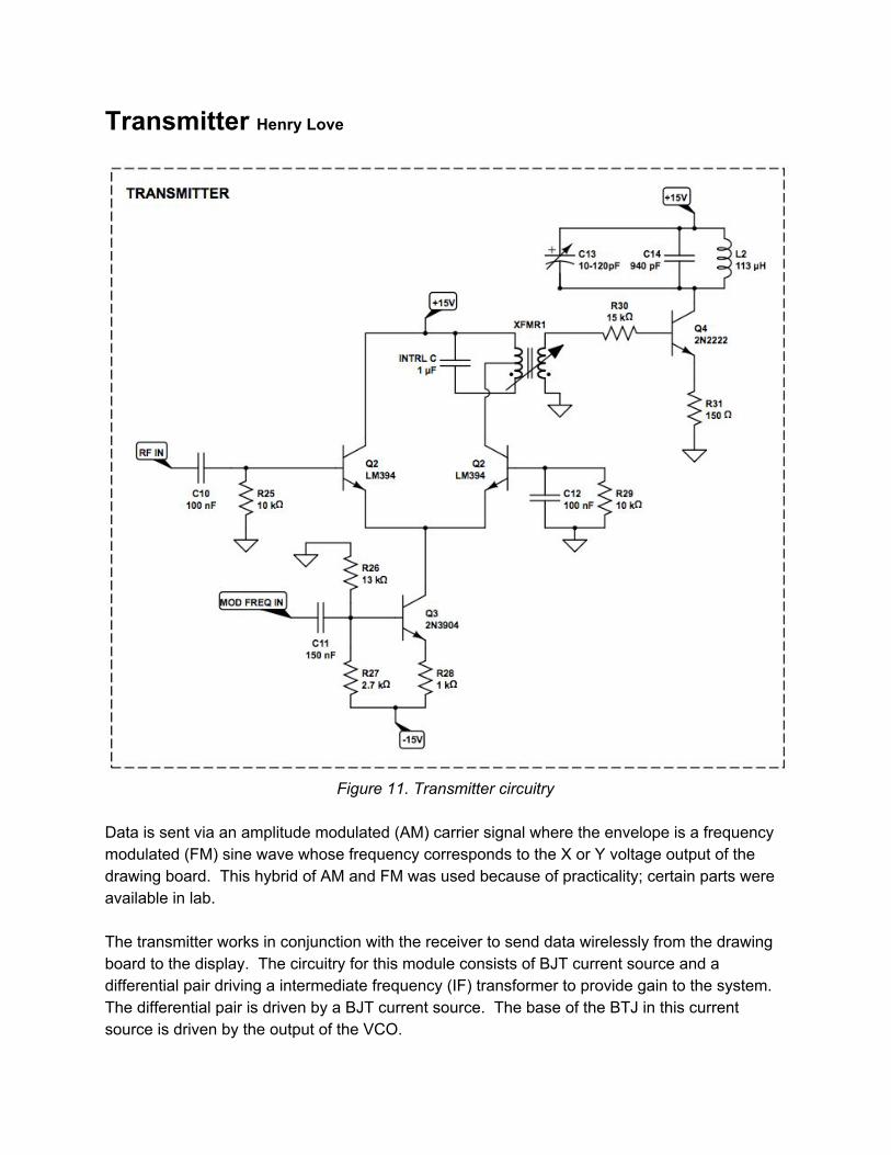
Figure 11. Transmitter circuitry
Data is sent via an amplitude modulated (AM) carrier signal where the envelope is a frequency modulated (FM) sine wave whose frequency corresponds to the X or Y voltage output of the drawing board. This hybrid of AM and FM was used because of practicality; certain parts were available in lab. The transmitter works in conjunction with the receiver to send data wirelessly from the drawing board to the display. The circuitry for this module consists of BJT current source and a differential pair driving a intermediate frequency (IF) transformer to provide gain to the system. The differential pair is driven by a BJT current source. The base of the BTJ in this current source is driven by the output of the VCO.
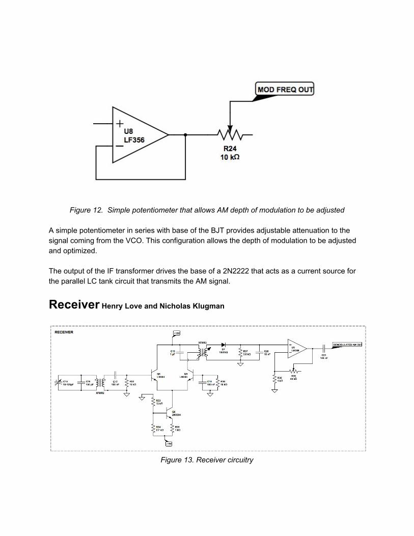
Figure 12. Simple potentiometer that allows AM depth of modulation to be adjusted
A simple potentiometer in series with base of the BJT provides adjustable attenuation to the signal coming from the VCO. This configuration allows the depth of modulation to be adjusted and optimized. The output of the IF transformer drives the base of a 2N2222 that acts as a current source for the parallel LC tank circuit that transmits the AM signal.
Receiver Henry Love and Nicholas Klugman
Figure 13. Receiver circuitry
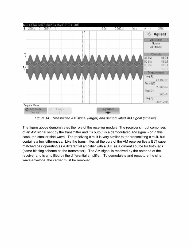
Figure 14. Transmitted AM signal (larger) and demodulated AM signal (smaller)
The figure above demonstrates the role of the receiver module. The receiver’s input comprises of an AM signal sent by the transmitter and it’s output is a demodulated AM signal - or in this case, the smaller sine wave. The receiving circuit is very similar to the transmitting circuit, but contains a few differences. Like the transmitter, at the core of the AM receiver lies a BJT super matched pair operating as a differential amplifier with a BJT as a current source for both legs (same biasing scheme as the transmitter). The AM signal is received by the antenna of the receiver and is amplified by the differential amplifier. To demodulate and recapture the sine wave envelope, the carrier must be removed.
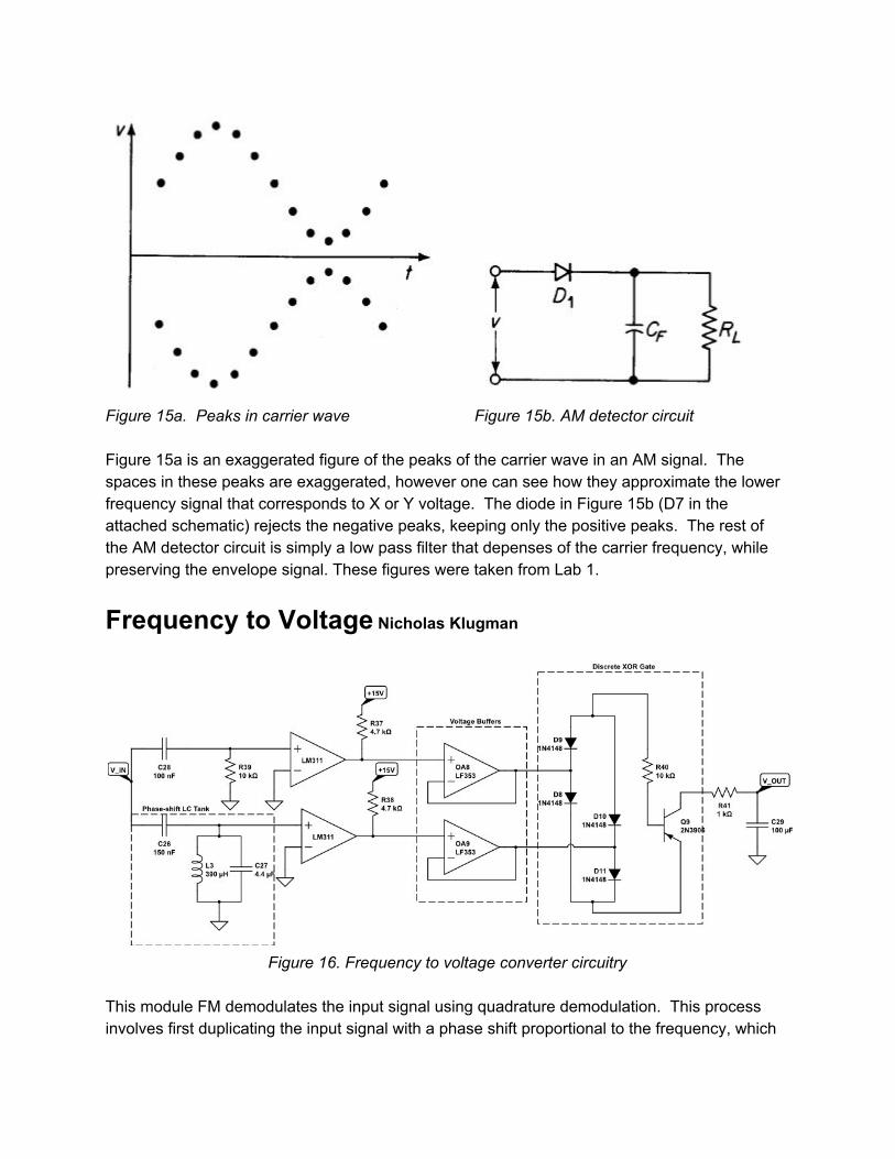
Figure 15a. Peaks in carrier wave Figure 15b. AM detector circuit
Figure 15a is an exaggerated figure of the peaks of the carrier wave in an AM signal. The spaces in these peaks are exaggerated, however one can see how they approximate the lower frequency signal that corresponds to X or Y voltage. The diode in Figure 15b (D7 in the attached schematic) rejects the negative peaks, keeping only the positive peaks. The rest of the AM detector circuit is simply a low pass filter that depenses of the carrier frequency, while preserving the envelope signal. These figures were taken from Lab 1.
Frequency to Voltage Nicholas Klugman
Figure 16. Frequency to voltage converter circuitry
This module FM demodulates the input signal using quadrature demodulation. This process involves first duplicating the input signal with a phase shift proportional to the frequency, which
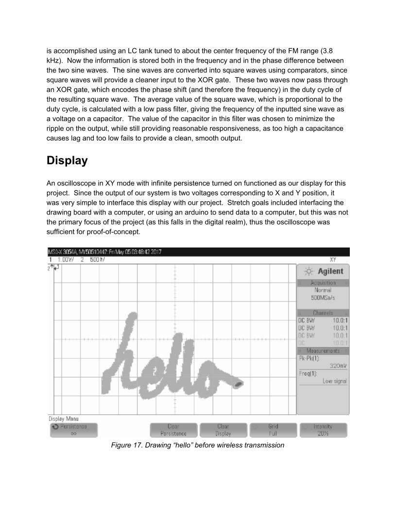
is accomplished using an LC tank tuned to about the center frequency of the FM range (3.8 kHz). Now the information is stored both in the frequency and in the phase difference between the two sine waves. The sine waves are converted into square waves using comparators, since square waves will provide a cleaner input to the XOR gate. These two waves now pass through an XOR gate, which encodes the phase shift (and therefore the frequency) in the duty cycle of the resulting square wave. The average value of the square wave, which is proportional to the duty cycle, is calculated with a low pass filter, giving the frequency of the inputted sine wave as a voltage on a capacitor. The value of the capacitor in this filter was chosen to minimize the ripple on the output, while still providing reasonable responsiveness, as too high a capacitance causes lag and too low fails to provide a clean, smooth output.
Display An oscilloscope in XY mode with infinite persistence turned on functioned as our display for this project. Since the output of our system is two voltages corresponding to X and Y position, it was very simple to interface this display with our project. Stretch goals included interfacing the drawing board with a computer, or using an arduino to send data to a computer, but this was not the primary focus of the project (as this falls in the digital realm), thus the oscilloscope was sufficient for proof-of-concept.
Figure 17. Drawing “hello” before wireless transmission
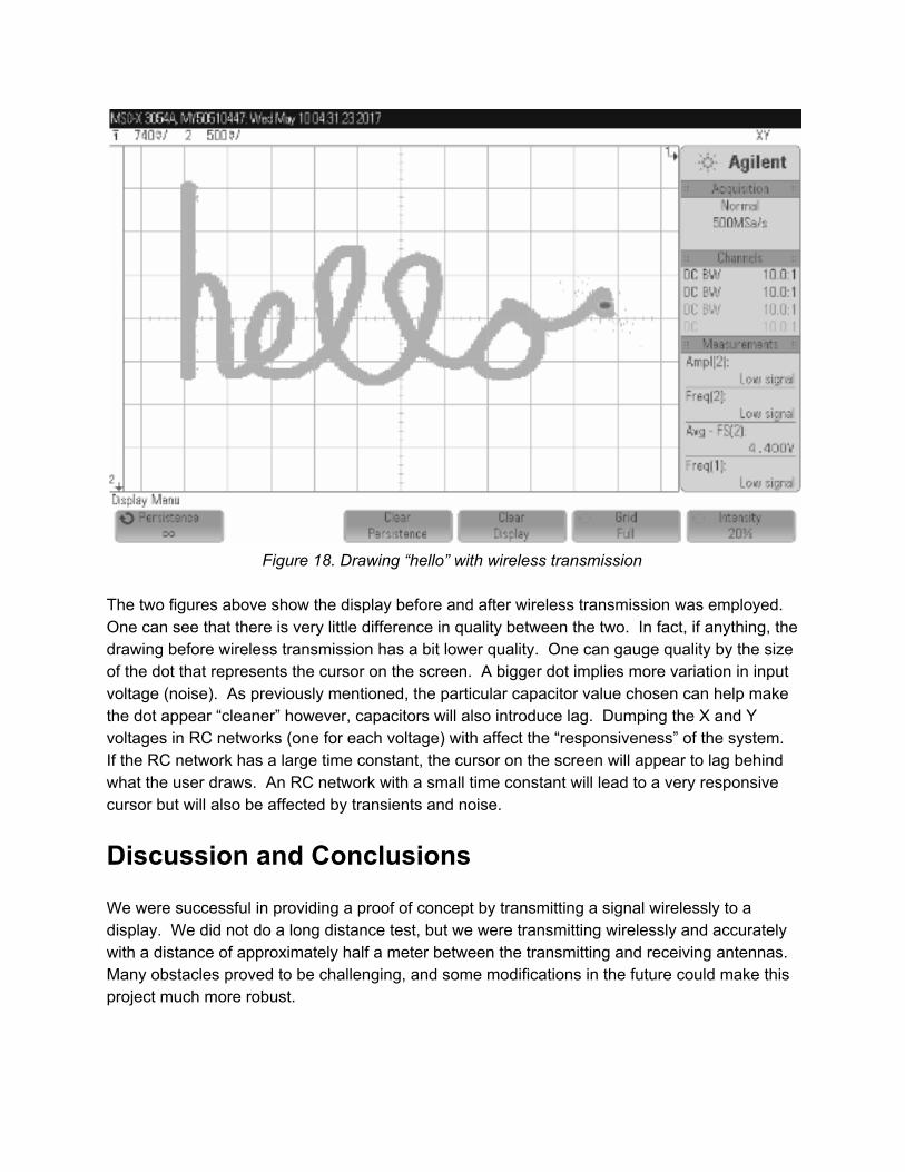
Figure 18. Drawing “hello” with wireless transmission
The two figures above show the display before and after wireless transmission was employed. One can see that there is very little difference in quality between the two. In fact, if anything, the drawing before wireless transmission has a bit lower quality. One can gauge quality by the size of the dot that represents the cursor on the screen. A bigger dot implies more variation in input voltage (noise). As previously mentioned, the particular capacitor value chosen can help make the dot appear “cleaner” however, capacitors will also introduce lag. Dumping the X and Y voltages in RC networks (one for each voltage) with affect the “responsiveness” of the system. If the RC network has a large time constant, the cursor on the screen will appear to lag behind what the user draws. An RC network with a small time constant will lead to a very responsive cursor but will also be affected by transients and noise.
Discussion and Conclusions We were successful in providing a proof of concept by transmitting a signal wirelessly to a display. We did not do a long distance test, but we were transmitting wirelessly and accurately with a distance of approximately half a meter between the transmitting and receiving antennas. Many obstacles proved to be challenging, and some modifications in the future could make this project much more robust.
The two colpitts oscillators provided carriers at 470kHz and 535kHz. The IF transformers used in this project had a range of approximately 330kHz to 540kHz. Because of this, the 535kHz oscillator was operating at the upper frequency of what the IF transformer was designed for. This caused the 535kHz transmitted signal to have smaller amplitude than the 470kHz carrier when amplified by the differential amplifier in the transmitter circuit. It was also discovered that while transmitting the signals, occasionally, one transmitting antenna would couple to the other and introduce noise at the other antenna's resonant frequency. Mounting the two antennas at 90 degrees to each other minimized this noise and was the most successful antenna configuration when transmitting both signals. In the future, it would be interesting to combine both transmitting channels into one channel comprising of one carrier frequency. This would minimize the need for duplicate hardware and also eliminate the coupling problem encountered while using two antennas. Due to the nature of data acquisition requiring a multiplexed X and Y signal to begin with, it may be possible to send this initial signal and reverse multiplex it on the receiving side. One complication with this practice, however, is that the precise switching timing is known at the transmitter, but not the receiver. However, the fact that the X and Y voltages can never take on the same value could make this problem simpler. It would also be interesting to look into transmitting the signal purely using FM. In this project, we amplitude modulate a carrier wave with a frequency modulated sine wave as the envelope. One may ask, why even bother with the AM? --And that is a valid question. The transmitting scheme presented in this report was appealing as we both had prior knowledge of transmitting AM signals and knew that the necessary hardware was available in lab (such as antennas and IF transformers). Using purely FM, the amount of hardware used for this project may be decreased and some stages of the circuitry could possibly be eliminated. However for providing a proof of concept in a limited period of time, the encoding scheme used was sufficient. Additional features may be added to the project for future renditions, such as an auto location button, where if pressed, the cursor would move to a fixed location on the screen.
Q2LM394
Q2LM394
Q32N3904
R281 k
R272.7 k
R2613 k
C12100 nF
R2910 k
C10100 nF
R2510 k
+15V
-15V
C11150 nF
RF IN
MOD FREQ IN
XFMR1
U7LM311
U6LM6132
R157.5 k
R1610 k
M12N7000
R1810 k
R173.74 k
U5LM6132R14
10 k
R2010 k
R2110 k
R1910 k
C74.7 µF
C833 nF
Q12N2222
L148.7 µH
C44.7 nF
C54.7 nF
R910 k
U1LF356C1
470 nF
R31 k
R21 k
D31N4001
D21N4001
D11N4001
D41N4001
Drawing Pad
C21 µF
R4250 k
C31 µF
R5250 k
D51N4148
D61N4148
Pencil
Q5LM394
Q5LM394
Q62N3904
R351 k
R342.7 k
R3313 k
C18100 nF
R3610 k
C17100 nF
R3210 k
+15V
-15V
XFMR3
XFMR2
C1510-120pF
C16100 pF
C191 µF
INTRL C1 µF
D71N4148 R37
3.6 kC2010 nF
U9LM358
R381 k
R3950 k
C21100 nF
U8LF356
R232.7 k
C947 nF
+15V
+15V
+15V
SCALED VOLTAGE IN
X VOLTAGE OUT Y VOLTAGE OUT
MOD FREQ OUT
RF OUT
R3015 k
Q42N2222
L2113 µH
C14940 pF
R31150
+15V
+15V
C23150 nF
L3390 µH
C244.4 µF
R414.7 k
+15V
R424.7 k
+15VC22100 nF
R4010 k
U12LF353
U13LF353
D81N4148
D91N4148
D101N4148
D111N4148
Q92N3906
R4310 k
R441 k
C25100 µF
DEMODULATED AM OUT
DEMODULATED AM IN
U4LM6132C6
470 pF
R121 k
R1310 k
R224.7 k
R110 k
R1110 k
R1010 k
R2410 k
R810 k
R72.7 k
R610 k
U3LF353
+15V
U1LM310
SCALED VOLTAGE OUTX, Y VOLTAGE IN
C1310-120pF
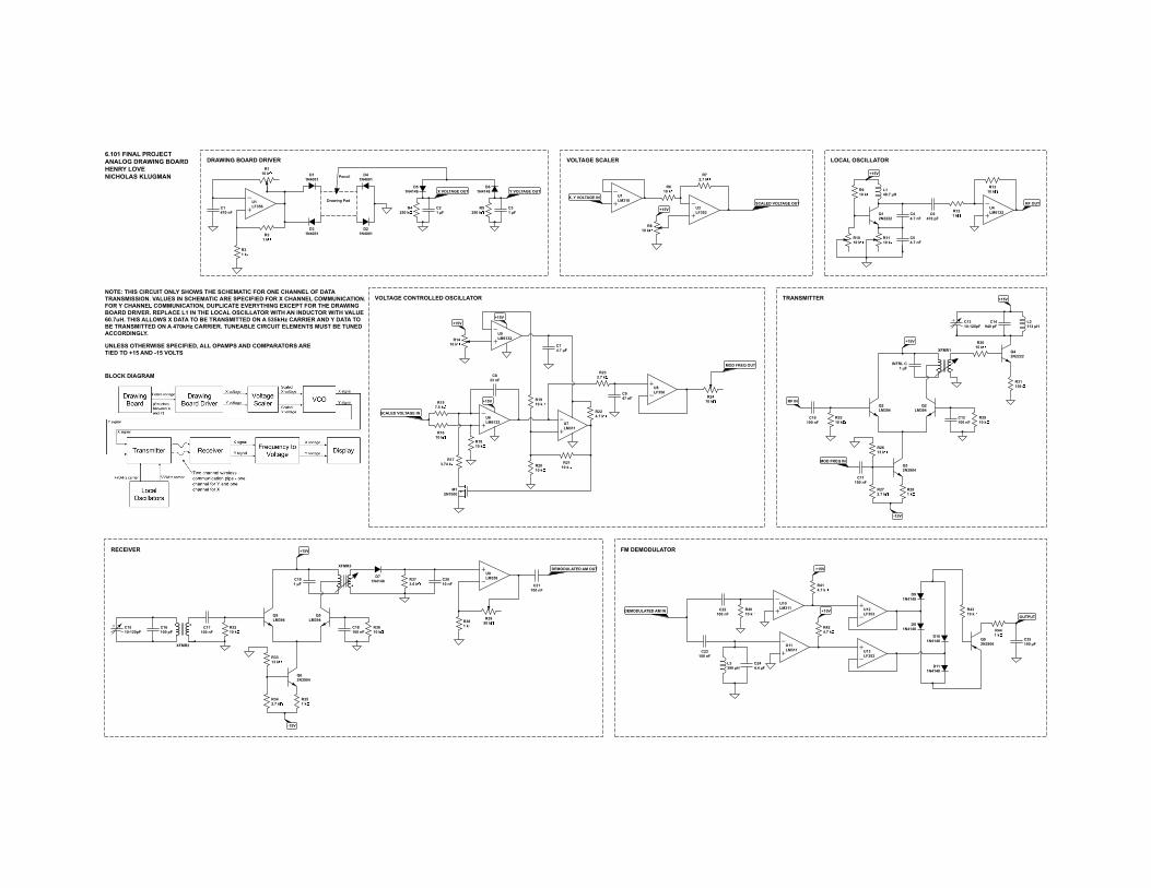
DRAWING BOARD DRIVER VOLTAGE SCALER LOCAL OSCILLATOR
VOLTAGE CONTROLLED OSCILLATOR TRANSMITTER
RECEIVER FM DEMODULATOR
OUTPUT
6.101 FINAL PROJECTANALOG DRAWING BOARDHENRY LOVENICHOLAS KLUGMAN
NOTE: THIS CIRCUIT ONLY SHOWS THE SCHEMATIC FOR ONE CHANNEL OF DATATRANSMISSION. VALUES IN SCHEMATIC ARE SPECIFIED FOR X CHANNEL COMMUNICATION.FOR Y CHANNEL COMMUNICATION, DUPLICATE EVERYTHING EXCEPT FOR THE DRAWINGBOARD DRIVER. REPLACE L1 IN THE LOCAL OSCILLATOR WITH AN INDUCTOR WITH VALUE60.7uH. THIS ALLOWS X DATA TO BE TRANSMITTED ON A 535kHz CARRIER AND Y DATA TOBE TRANSMITTED ON A 470kHz CARRIER. TUNEABLE CIRCUIT ELEMENTS MUST BE TUNEDACCORDINGLY.
U10LM311
U11LM311
UNLESS OTHERWISE SPECIFIED, ALL OPAMPS AND COMPARATORS ARETIED TO +15 AND -15 VOLTS
BLOCK DIAGRAM
Appendix
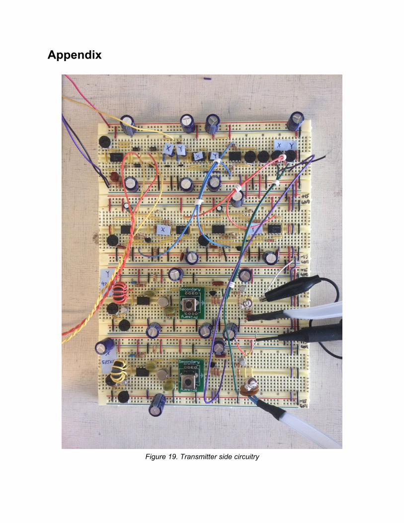
Figure 19. Transmitter side circuitry
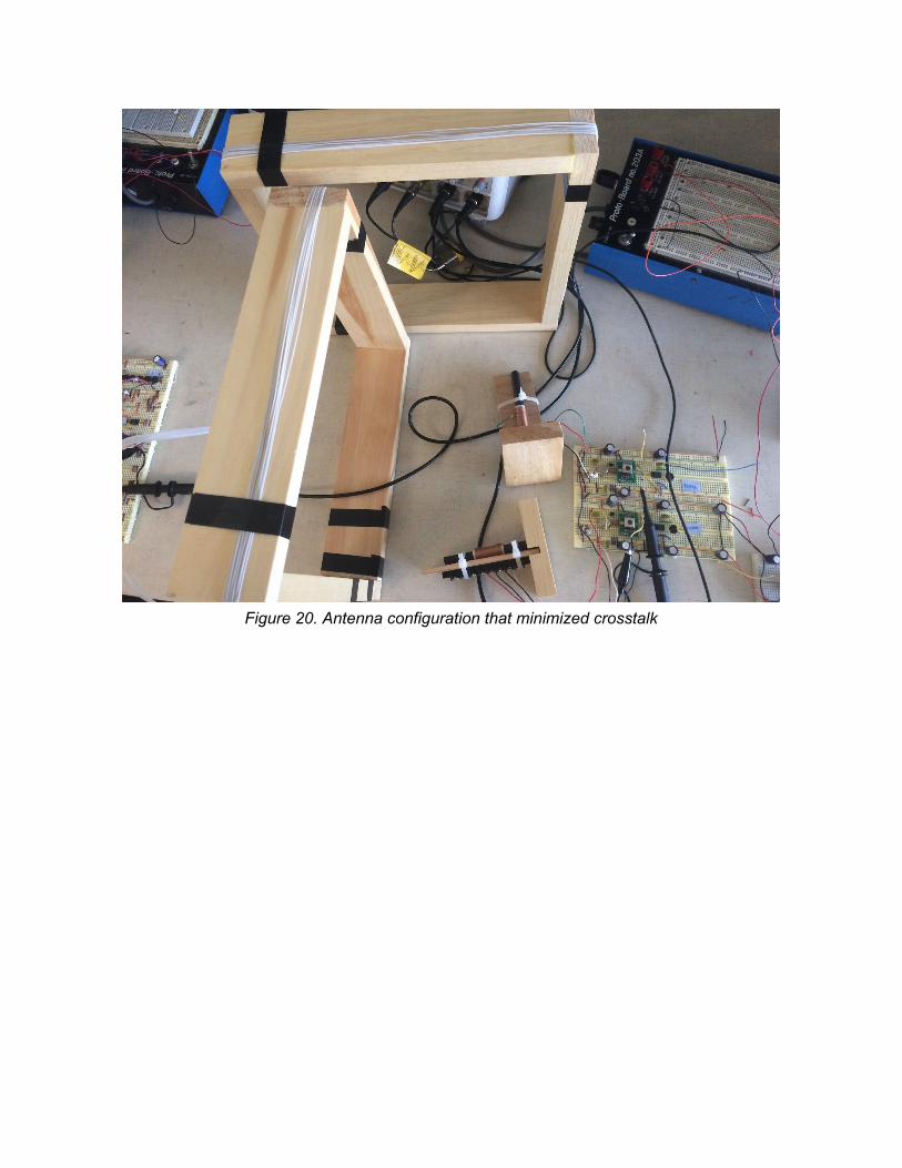
Figure 20. Antenna configuration that minimized crosstalk
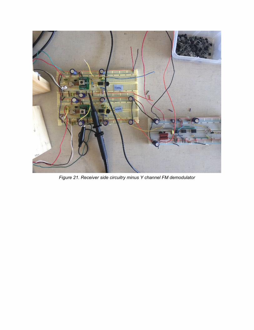
Figure 21. Receiver side circuitry minus Y channel FM demodulator
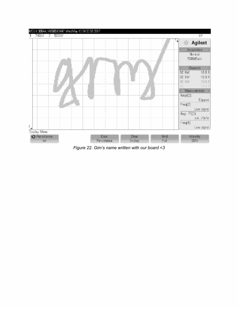
Figure 22. Gim’s name written with our board <3