Embed Size (px)
Citation preview

---Introduction of power-on-chip developmentPMU�SIMO�Embedded�Integrated�Wireless�Eco
Bill Yang Liu
Prof. Hong ZhiLiang
Weiwei Xu, Bin Shao
Analog Devices & Fudan University

Introduction of the power-on-chip development
1)PMU
2)SIMO
3)Embedded Power
4)Integrated Power
5)More

Power
Management
Chip 1
System Chip
Power
Management
Chip 2
Induct/Cap/Res
A System Solution in Portable Applications
Induct/Cap/Res

4
Power Management Units (PMU)
• Integration to improve system flexibility
• Small package and small form of factor
– Cost reduction
• Package cost
• BOM cost
– Performance improvement
• Efficiency
• Easy sequence control

5
• Charger• Switching regulators
• buck• boost• buck/boost• inverter
• LDO• Backlight driver• Audio driver• Ambient light sensor• Touch panel sensor• RTC• Sequence control• Voltage monitor and
supervisory
Product Example
Ref: C. Shi, CICC 2006, pp. 85-88

6
Package Roadmap

7
WLCSP Solution
• Package size is as large as die size

8
BOM Reduction

9
PMU Topics
• Trend
– More functions/high density
– Smaller/thinner/cheaper package
– Higher frequency
• Issue
– Thermal
– Noise coupling and crosstalk
– Design challenge in high switching frequency
• Current sensing for current mode control

10
PMU Design Considerations
• System optimization, not chip optimization
• Power and analog supply separation
• Layout strategy
– Power stage position
– Crosstalk between channels
– Guardring and sensitive line routing

PMU
System Chip
Induct/Cap/Res
A System Solution in Portable Applications
Induct/Cap/Res
12
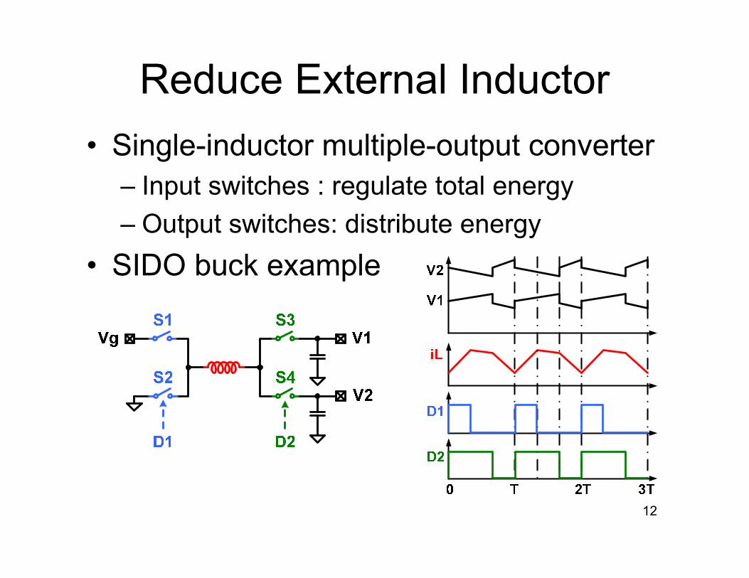
Reduce External Inductor
• Single-inductor multiple-output converter
– Input switches : regulate total energy
– Output switches: distribute energy
• SIDO buck example
13
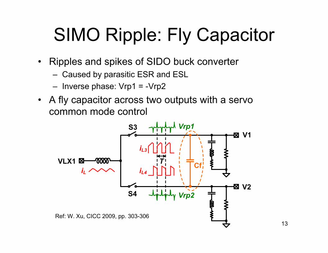
SIMO Ripple: Fly Capacitor
• Ripples and spikes of SIDO buck converter
– Caused by parasitic ESR and ESL
– Inverse phase: Vrp1 = -Vrp2
• A fly capacitor across two outputs with a servo
common mode control
V1
V2
S3
S4
iL3
iL4Cf
T
iL
VLX1
Vrp1
Vrp2
Ref: W. Xu, CICC 2009, pp. 303-306

14
Multi-Loop Feedback System

15
Extended-PWM (EPWM) control
Ref: W. Xu, ISSCC 2011

16
Loop Compensation
• Continuous vs. Discrete-time
Vfb2
Vrf2
Vfb1
Vrf1
Vbias Vea
1
2
1
2
1
1 1
1 1
2 2
2 2
Vrf2
Vrf1
Vfb1
Vfb2Vea
Ref: M. Belloni, ISSCC 2008, pp. 444-445

17
SIMO: Trade-off
Switching
Converter
Cost
Efficiency Size
Design
ComplexityRipple
Conventional
Converter
SIMO
Converter

PMU
System Chip
Induct/Cap/Res
A System Solution in Portable Applications
19
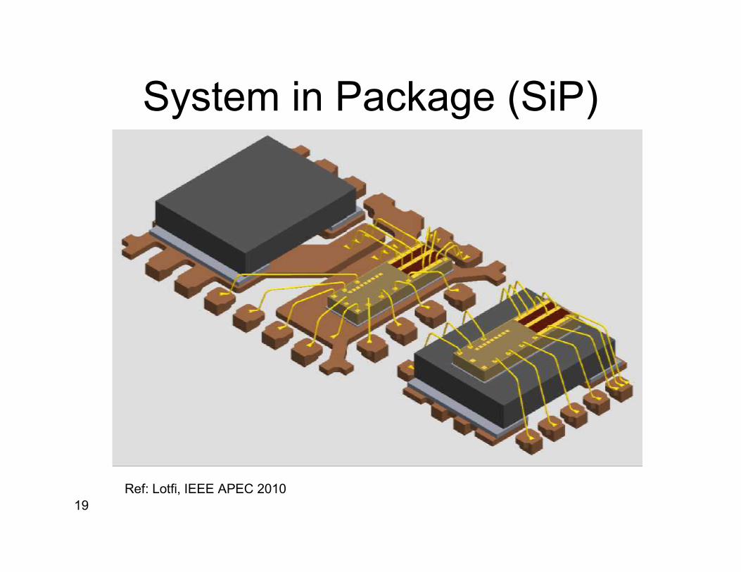
System in Package (SiP)
Ref: Lotfi, IEEE APEC 2010

20
SiP: Stack & Side
Controller + Power transistor Controller + Power transistor Regulator + Inductor
Ref: B. Chen, IEEE APEC 2010

21
SiP Technique
• Now
– Magnetic materials on silicon
• Inductance <100nH
• Switching frequency > 20MHz
– Regulator with integrated inductor
• Assembly with standard MCM process
• Future
– Increase the integration density
– Multi die to single die

22
Embedded Power
DSP
MCU
Embedded
Memory
Linear
Regulators
Battery
Charger
Digital Modulator
Digital
Filter
Digital
Filters &
Sample
Rate
Conversion
ADC
DAC
Audio
ADC
Audio
DAC
Receiver
Transmitter
Flash
Memory
SRAM
DBB (Digital) ABB (Mixed-Signal)
Audio (Mixed-Signal)
RF
PA
Power management
Memory
Switching
Regulators
Communication Accelerators

23
Class G / Class I
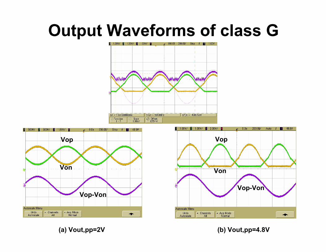
Output Waveforms of class G
(a) Vout,pp=2V (b) Vout,pp=4.8V
Vop
Von
Vop-Von
Vop
Von
Vop-Von

25
HV in MEMS
• Low Insertion Loss• High Linearity• High Isolation
• MEMS Gyroscope
– Mechanical Structure of gyro needs to be driven by HV
electrostaticsly.
– Coriolis signal ∝ Force ∝ V2
– Increased SNR

26
How to Generate the HV
• Inductor based
– Expensive
– Two pinouts
• Capacitor based
– One pinout
– Integrated capacitor can be used as the MEMS
capacitance drops while its process improves
– ~100uA

27
Integrated HV Charge Pump
Resistor d
ivider

28
Other Applications of HVCP
• E2PROM
• Flash Memory
• MEMS Switches
• Liquid Crystal Lens Driver
• More...

PMU
System Chip
Induct/Cap/Res
A System Solution in Portable Applications

Vin
Vout
MP
MN
Vramp
Vref
z1 z2
Error
amplifierPWM
comparator
Gate
driver
Motivation
• Integrated DC-DC converters are needed
with SOC and on-chip power scaling
On-chip Off-chip

1 10 100 1000
0
0.5
1
1.5
2
2.5
3
3.5
L (µH)
Frequency (MHz)
L≈1 µH, fsw=3 MHz
L≈10 nH, fsw=200 MHz
Inductance vs Frequency
( )out in out
in sw o
V V VL
V f I
× −=
× ×
Challenge: low Quality factor results in low power efficiency
On-chip Inductor

Q-factor vs Power Efficiency
• Parasitic resistances
– Metal resistance: Rs
– Substrate resistance: Re2
con rmsP I R= ×
2sw swP C V f= × ×
• Parasitic capacitances
– Spiral-to-substrate capacitance: Cox
– Spiral-to-underpass overlap capacitance: Cf

Port1 Port2
Top View of the Inductor
• Number of sides=16
• Number of turns=2.75
• Metal width=100 µm
• Inner diameter=800 µm
22 W××××Overlap area:

Cross-section View
M8
M7
– Basic structure, low quality factor
– We should take advantage of the eight copper
layers available in the process!
Port1
Port2

Multi-layer Winding
M8
M7
M6
M5
M4
M3– Multi-layer winding can reduce the
series resistance Rs
Port1
Port2

M6-to-M4 Spacing
M8
M7
M6
M4
M3
M2
– M6-to-M4 spacing can reduce the
overlap capacitance Cf
Port1
Port2

Patterned N-Well
– Reduce the electric and magnetic
coupling to the substrate
M8
M7
M6
M4
M3
M2
N-Well
Port1
Port2

Performance of the Inductor
Process Material L Rseries Cparasitic
JSSC07 [1] 0.35µm0.02 ΩΩΩΩ/squareAluminum
22nH 2.5 ΩΩΩΩ 25 pF
ESSCIRC08[5] 0.13µm2 µm Copper+
1.2 µm Aluminum9.8nH 1.6 ΩΩΩΩ —
CICC08[3] 0.18µm Golden bond wire 18nH 1 ΩΩΩΩ —
This work 0.13 µm3+0.385+0.385 µm
Copper10.5nH 1.2 ΩΩΩΩ 3 pF
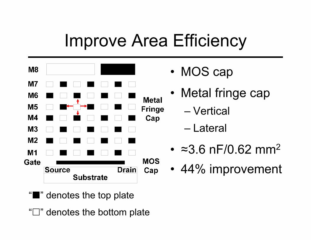
Improve Area Efficiency
“�” denotes the top plate
“�” denotes the bottom plate
• MOS cap
• ≈3.6 nF/0.62 mm2
• 44% improvement
• Metal fringe cap
– Vertical
– Lateral

Circuit Architecture
• Features
– Vin=3.3 V
– fs~250 MHz
– On-chip L
– On-chip Cout
– Buck converter

Chip Micro-photograph

Measured Power Efficiency
The input voltage is 3.3 V for all measurements
10
20
30
40
50
60
70
80
90
0 50 100 150 200 250 300 350 400
Load Current (mA)
Efficiency (%)
Vout=2.5 V
Vout=1.8 V
Vout=1.2 V

Compare LDO With Buck
The efficiency of LDO is prior to Buck at light loads, vice
versa.
75.0@ =Vin
Vout
43
Especially, when
the load current is
zero, the Buck
consumes more
than 10mW,
While the LDO
consumes less
than 1mW.

Proposed Structure
1.2V 50mV
Iload>IthIload<Ith
4.5nH
7n
44

LDO Consideration
nFCout 7=
Stability is difficult to design!
Dominant pole
Non-dominant pole
45
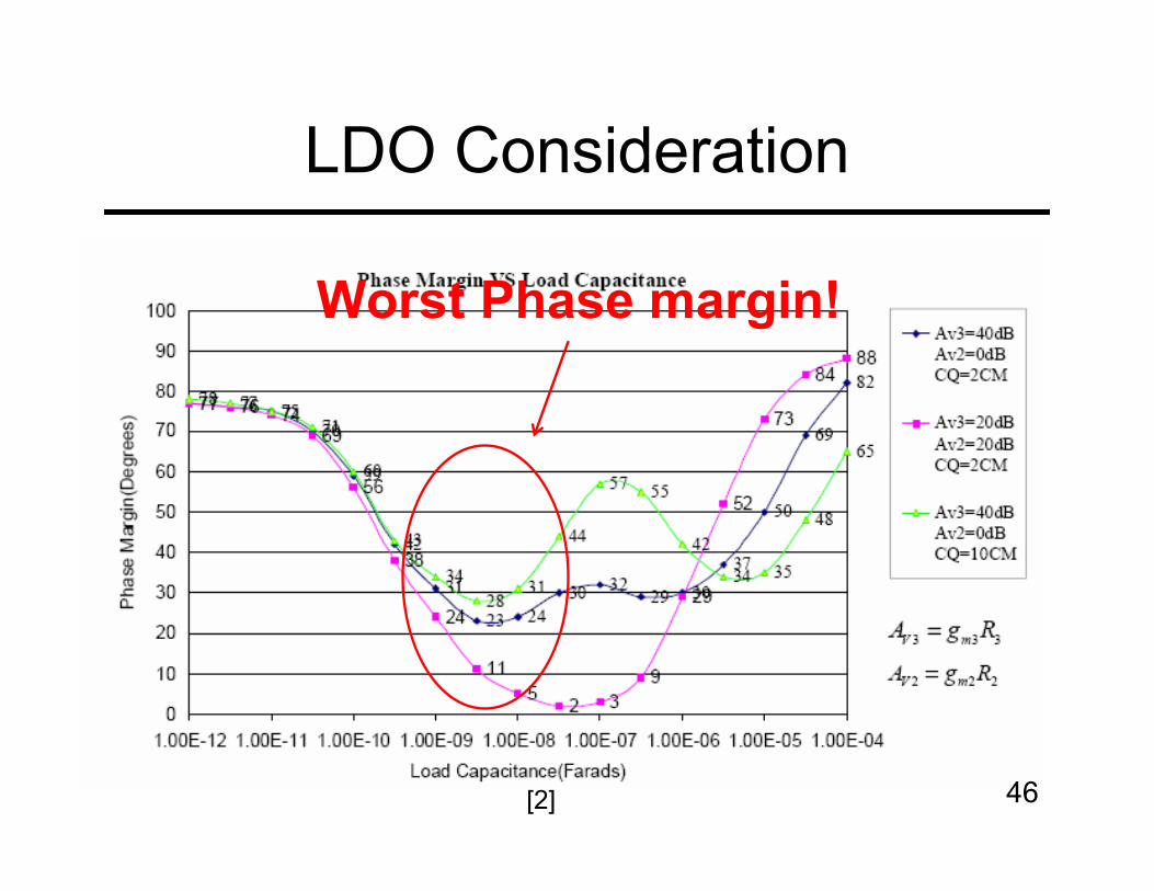
LDO Consideration
[2]
Worst Phase margin!
46

Analysis of LDO
Adaptively Adjust P3
First stage
•Large quiescent current to
put P3 to high frequency
•Static condition is hard to
control---Vth5 , R4 , I6
47

Adaptive P3 Adjust Circuit.
IQ
48
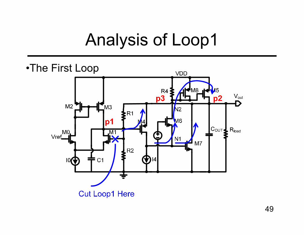
Analysis of Loop1
•The First Loop
49

Transfer Function of Loop1
gm1
1x
gm6
Cp5 R4//(1/gm8)1/gm6
gm5
CL Roeq
VOUT
B
C1 ro1
gm4
gm7gm4
Cut Loop
Here
•CL>>C1>Cp5
8
44
1//
mgRZ =
)1)(1)(1(
)1))/1((
(
))/()(1(
)))/1((()(
544
4511
5
675
11
5446744545
2
11
5446744511
+++
++
•
≈
++++
++•≈
mm
outpop
m
mmp
om
oeqmmoeqoutmmoeqmpoeqpoutop
oeqmmmmoeqmpom
gZg
sCZsCrsC
sg
ggCrBg
RgZgRCggRgZCsZRCCsrsC
RgZgsggRgZCrBgsT
50

Full Load
Condition
GBW=100K
PM=82 degree
No Load
Condition
GBW=100K
PM=86 degree
Bode Plot of Loop1
16
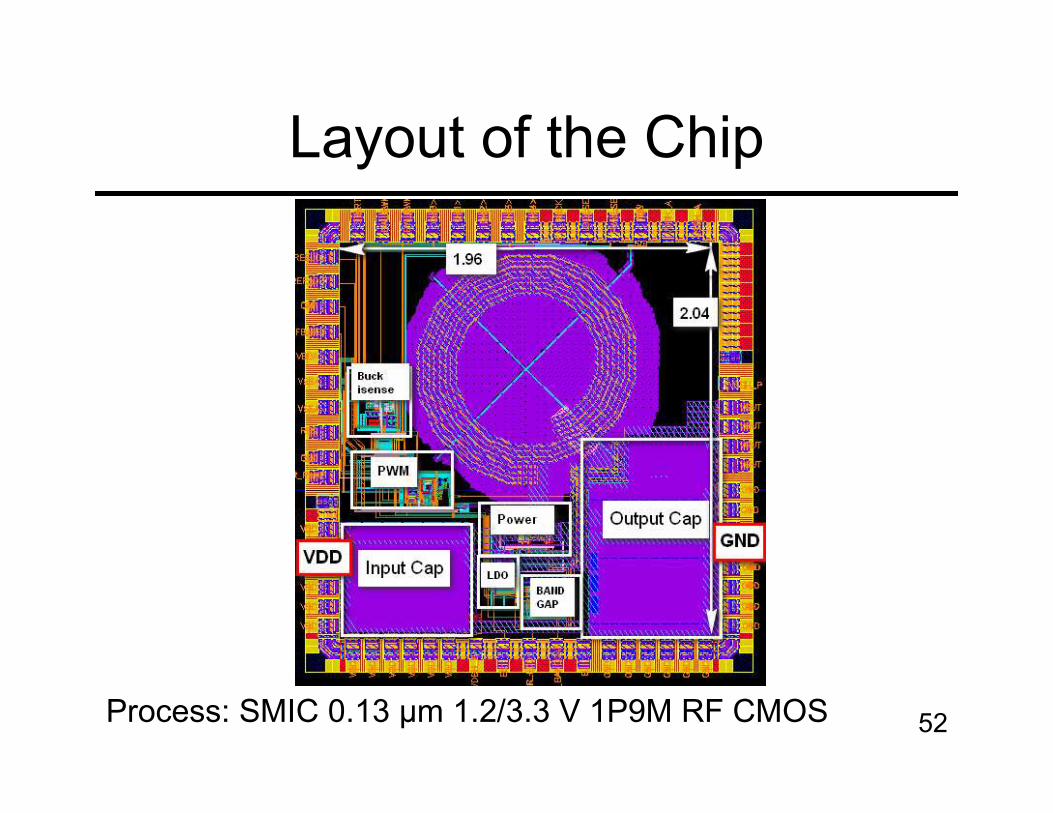
Layout of the Chip
Process: SMIC 0.13 µm 1.2/3.3 V 1P9M RF CMOS 52
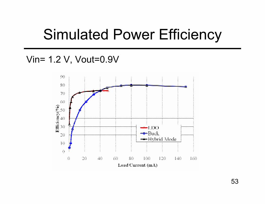
Simulated Power Efficiency
Vin= 1.2 V, Vout=0.9V
53

More…To be really invisible

PMU
System Chip
Induct/Cap/Res
A System Solution in Portable Applications
PMU
System Chip
Induct/Cap/Res
System 1 System 2

56
Wireless Power
• Wireless signal � Wireless power

57
Not a New Topic
Tesla’s high frequency and potential lecture of 1891

58
But an Emerging Market
Source: iSuppli Corp. 2010
• Mobile phone market drives the growth

PMU
System Chip
Induct/Cap/Res
A System Solution in Portable Applications
System 1 Energy
Source
60
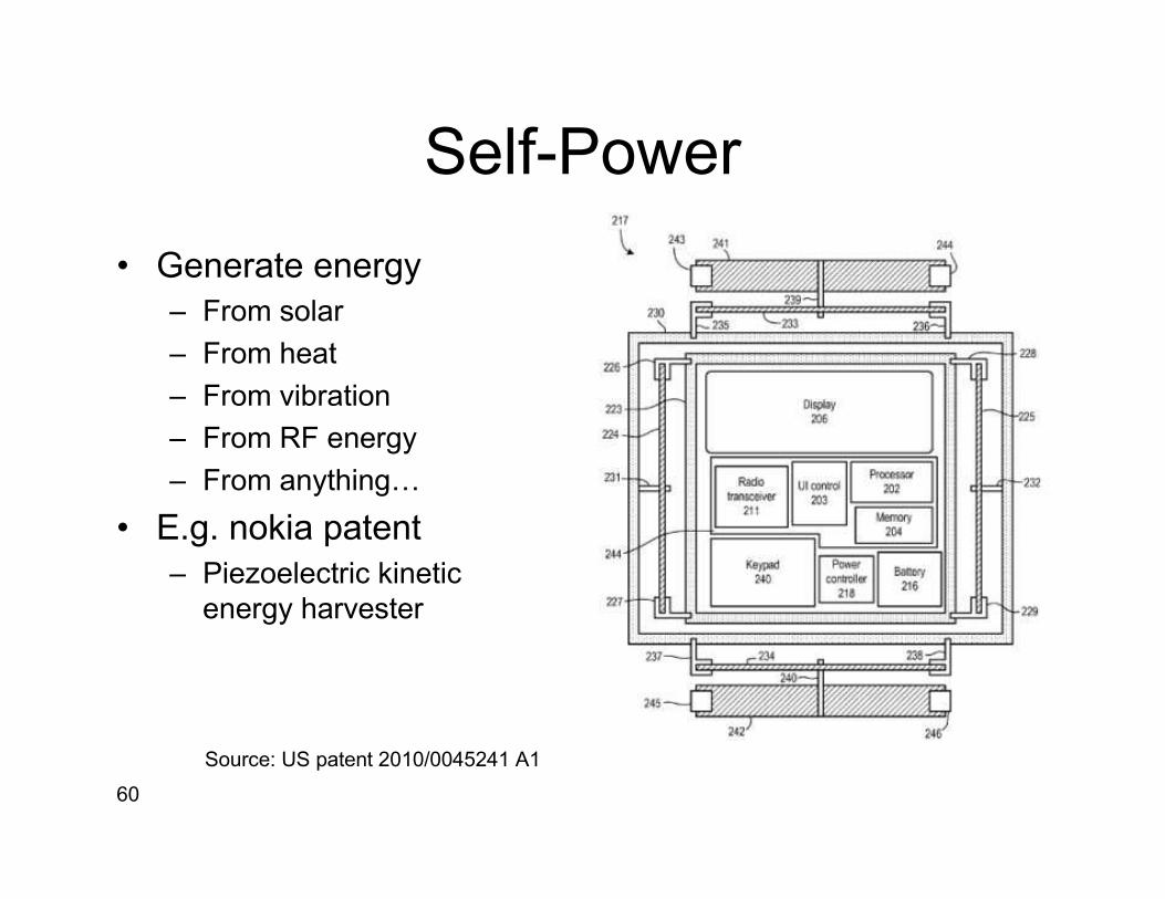
Self-Power
• Generate energy
– From solar
– From heat
– From vibration
– From RF energy
– From anything…
• E.g. nokia patent
– Piezoelectric kinetic
energy harvester
Source: US patent 2010/0045241 A1

61
EE: Energy Engineering
• Energy generation
– Solar energy
– Piezoelectric energy
• Energy transmission
– Non-isolated power stage
– Wireless power
• Energy conversion
– Linear vs. Switching
– Inductor based vs. Charge pump

PMU
System Chip
Induct/Cap/Res
Advanced Power Management Techniques for Portable Applications
System 1 Energy
Source
The power-invisible solution…
Green Power