Embed Size (px)
Citation preview
Analog and Mixed-Signal VLSI Design Center
IOWA STATE UNIVERSITY1
Role of Op-AmpsRole of Op-Amps
• widely used building blocks for analog circuits
• widely used in communication circuits• Widely used in analog signal processing
– critical block for data-converters• Widely Used in High Volume ICs
– memory read out– Disk-driver reading-writing

Analog and Mixed-Signal VLSI Design Center
IOWA STATE UNIVERSITY2
New challenges in Analog DesignNew challenges in Analog Design
• Decreased Supply Voltage• Increased Digital/Analog Interference• Reduced Testability• Increased Parametric Variations
Analog and Mixed-Signal VLSI Design Center
IOWA STATE UNIVERSITY3
Critical Specifications for Op-AmpsCritical Specifications for Op-Amps
• High DC Gain
• High Speed/Large Gain-Bandwidth
• Sufficient Output Swing
• High power efficiency
Desirable: digital built-in-self-test and self-calibrationDesirable: digital built-in-self-test and self-calibration
Analog and Mixed-Signal VLSI Design Center
IOWA STATE UNIVERSITY4
Existing structures & LimitationsExisting structures & Limitations
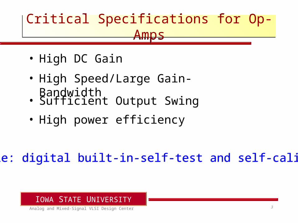
Cascode Amplifier
DC Gain: Modest
Speed: Excellent
Output Swing: Small
Power Efficiency: Good
Vi2
M4
Mb
M1 M1
M3 M3
Vi1
M2 M2
M4
bias1
bias2
bias3
cmfb
Frequency Response: Good
Analog and Mixed-Signal VLSI Design Center
IOWA STATE UNIVERSITY5
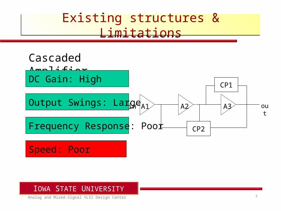
Existing structures & LimitationsExisting structures & Limitations
Cascaded Amplifier
DC Gain: High
Output Swings: Large
Speed: Poor
CP1
CP2
in outA1 A2 A3
Frequency Response: Poor
Analog and Mixed-Signal VLSI Design Center
IOWA STATE UNIVERSITY6
Existing structures & LimitationsExisting structures & Limitations
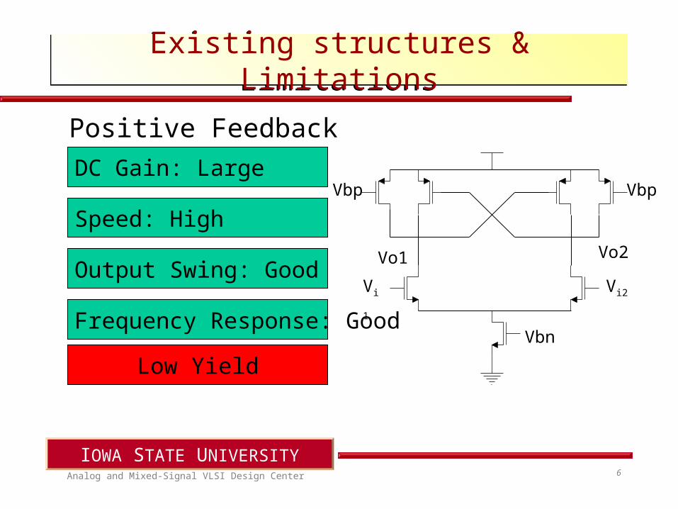
Positive Feedback AmplifierDC Gain: Large
Output Swing: Good
Speed: High
Low Yield
Frequency Response: Good
Vi1 Vi2
Vbn
Vbp Vbp
Vo1 Vo2
Analog and Mixed-Signal VLSI Design Center
IOWA STATE UNIVERSITY7
Our ObjectiveOur Objective
• Low Voltage Compatible• High DC Gain• High Speed• Good Output Swing• High Yield• Standard Digital Process Compatible• Good Power Efficiency
Analog and Mixed-Signal VLSI Design Center
IOWA STATE UNIVERSITY8
Our ApproachOur Approach
• Find new amplifier architectures• Rely on digital logic to enhance
performance• Use simple digital circuit sensing amplifier
performance• Integrate controllability• Use adaptive feedback control
Analog and Mixed-Signal VLSI Design Center
IOWA STATE UNIVERSITY9
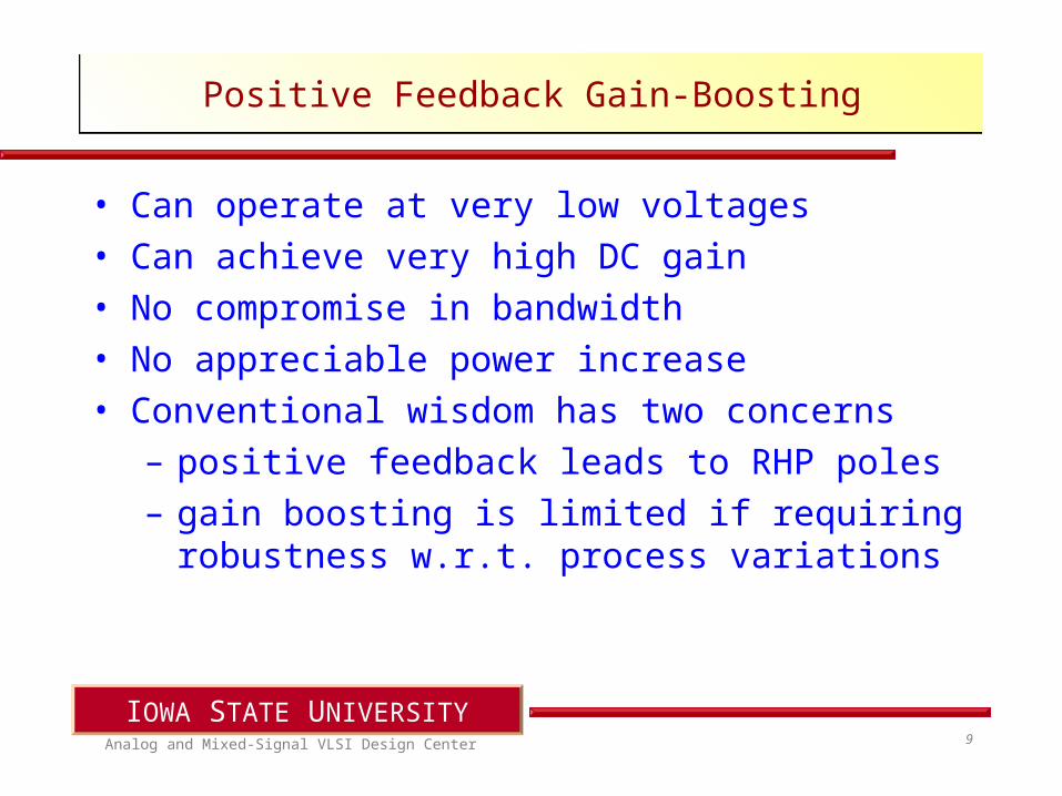
Positive Feedback Gain-BoostingPositive Feedback Gain-Boosting
• Can operate at very low voltages
• Can achieve very high DC gain
• No compromise in bandwidth
• No appreciable power increase
• Conventional wisdom has two concerns
– positive feedback leads to RHP poles
– gain boosting is limited if requiring robustness w.r.t. process variations
Analog and Mixed-Signal VLSI Design Center
IOWA STATE UNIVERSITY10
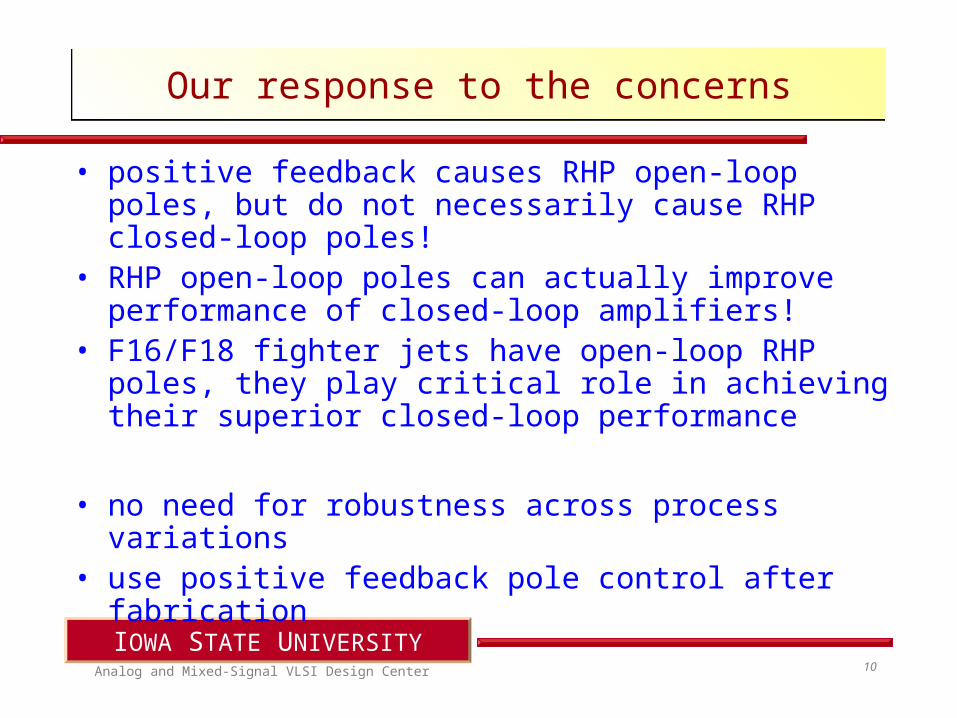
Our response to the concernsOur response to the concerns
• positive feedback causes RHP open-loop poles, but do not necessarily cause RHP closed-loop poles!
• RHP open-loop poles can actually improve performance of closed-loop amplifiers!
• F16/F18 fighter jets have open-loop RHP poles, they play critical role in achieving their superior closed-loop performance
• no need for robustness across process variations• use positive feedback pole control after fabrication
Analog and Mixed-Signal VLSI Design Center
IOWA STATE UNIVERSITY11
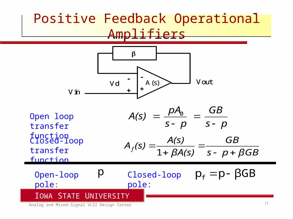
Positive Feedback Operational AmplifiersPositive Feedback Operational Amplifiers
A(s)
-
+Vin
-
+Vd VoutA(s)
-
+Vin
-
+Vd Vout
Open loop transfer function ps
GB
ps
pAA(s)
0
Closed-loop transfer function βGBps
GB
βA(s)
A(s)(s)Af
1
Open-loop pole: Closed-loop pole: βGBppf p
Analog and Mixed-Signal VLSI Design Center
IOWA STATE UNIVERSITY12
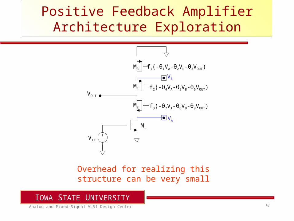
Positive Feedback Amplifier Architecture ExplorationPositive Feedback Amplifier Architecture Exploration
• Some positive feedback amplifier architectures have a dc gain that is much more sensitive to the feedback control variable than others
• Although architecture optimality may be difficult to determine, synthesis techniques may yield better structures than those already considered
• Comparative study of several structures with existing positive feedback structures
Analog and Mixed-Signal VLSI Design Center
IOWA STATE UNIVERSITY13
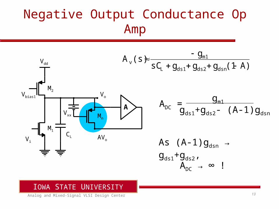
A)(1gggsC
g(s)A
dsnds2ds1L
m1v
Vdd
Vi
Vbias1 Vo
M1
M2
AVxx
CL
Mn
AVo
ADC = gm1
gds1+gds2- (A-1)gdsn
As (A-1)gdsn → gds1+gds2,
ADC → ∞ !
Negative Output Conductance Op Amp
Analog and Mixed-Signal VLSI Design Center
IOWA STATE UNIVERSITY14
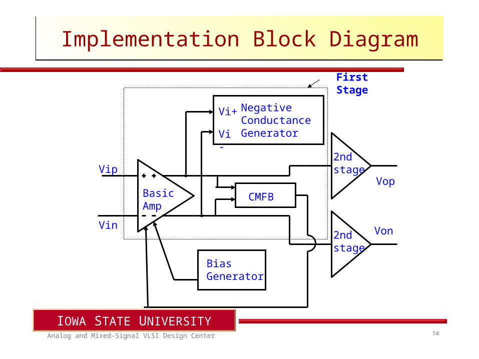
Implementation Block DiagramImplementation Block Diagram
Bias Generator
CMFB
Vip
Vin Von
VopBasic Amp
2nd stage
Negative Conductance GeneratorVi-
Vi+
2nd stage
First Stage
Analog and Mixed-Signal VLSI Design Center
IOWA STATE UNIVERSITY15
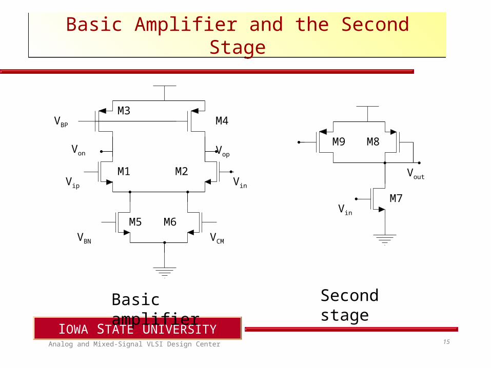
Basic Amplifier and the Second StageBasic Amplifier and the Second Stage
Basic amplifier Second stage
VBP
Vin
VCMVBN
Vip
Von Vop
M1
M5
M4M3
M2
M6Vin
M8M9
M7
Vout
Analog and Mixed-Signal VLSI Design Center
IOWA STATE UNIVERSITY16
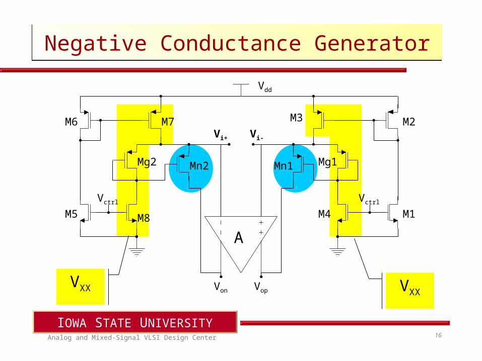
Negative Conductance GeneratorNegative Conductance Generator
Vdd
M1
VopVon
Vctrl
A
M5
Mg1Mn1
M4
M3 M2
Mn2
M8
M7M6
Mg2
Vi+ Vi-
Vctrl
VXX VXX
Analog and Mixed-Signal VLSI Design Center
IOWA STATE UNIVERSITY17
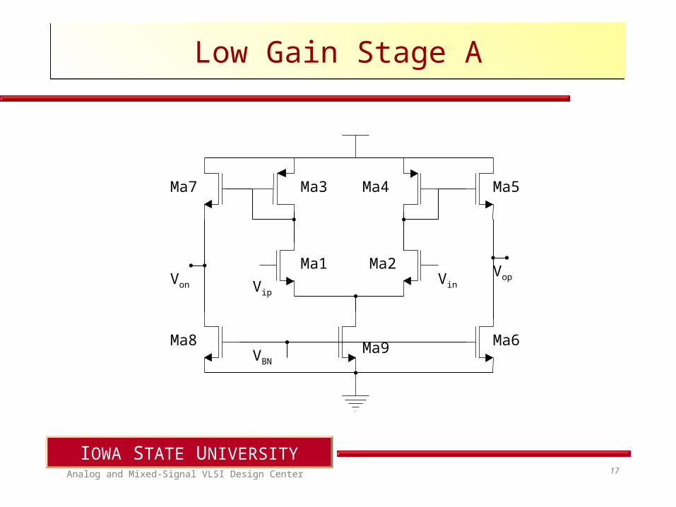
Low Gain Stage ALow Gain Stage A
Vin
VBN
Vip
VopMa1
Ma3
Ma2Von
Ma4
Ma8
Ma5
Ma6
Ma7
Ma9
Analog and Mixed-Signal VLSI Design Center
IOWA STATE UNIVERSITY18
Positive Feedback Amplifier Architecture Exploration
Positive Feedback Amplifier Architecture Exploration
VOUT
VIN
M1
M2
M3
M4
VA
VB
f1(-θ1VA-θ2VB-θ3VOUT)
f2(-θ4VA-θ5VB-θ6VOUT)
f3(-θ7VA-θ8VB-θ9VOUT)
Overhead for realizing this structure can be very small
Analog and Mixed-Signal VLSI Design Center
IOWA STATE UNIVERSITY19
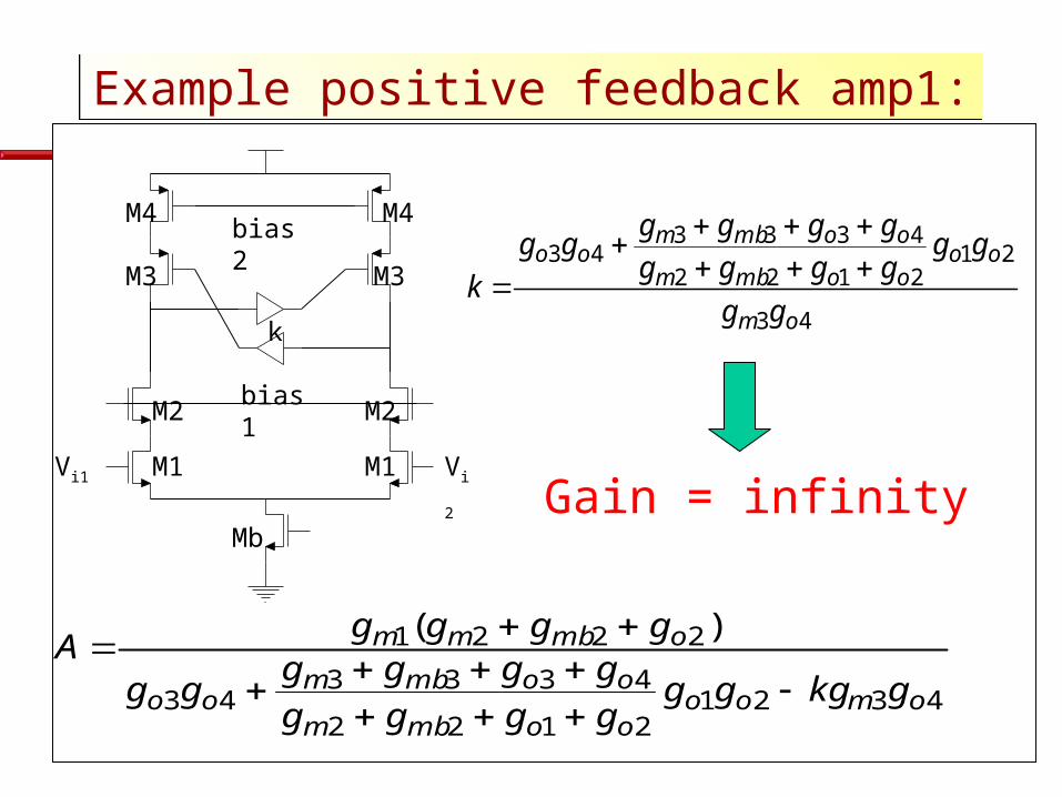
43212122
433343
2221 )(
omoooombm
oombmoo
ombmm
gkggggggg
gggggg
ggggA
Mb
M1 M1
M3 M3
k
Vi1 Vi2
M2 M2
M4 M4
bias1
bias2
Example positive feedback amp1:Example positive feedback amp1:
43
212122
433343
om
oooombm
oombmoo
gg
gggggg
gggggg
k
Gain = infinity
Analog and Mixed-Signal VLSI Design Center
IOWA STATE UNIVERSITY20
2122
12
2122
21
4333
43
2122
2221
oombm
om
oombm
oo
oombm
oo
oombm
ombmm
i
o
gggg
gkg
gggg
gg
gggg
gggggg
gggg
v
v
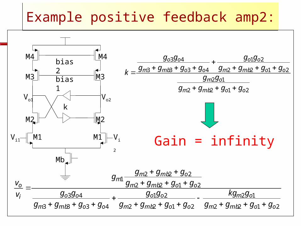
Example positive feedback amp2:Example positive feedback amp2:
Mb
M1 M1
M3 M3
k
Vi1 Vi2
M2 M2
M4 M4
bias1
bias2
Vo1 Vo2
2122
12
2122
21
4333
43
oombm
om
oombm
oo
oombm
oo
gggg
gggggg
gg
gggg
gg
k
Gain = infinity
Analog and Mixed-Signal VLSI Design Center
IOWA STATE UNIVERSITY21
M4
Mb
M1 M1
M3 M3
k
Vi1 Vi2
M2 M2
M4
bias1
bias2
422122
321
2122
433343
2221 )(
oooombm
moo
oombm
oombmoo
ombmm
gggggg
gkgg
gggg
gggggg
ggggA
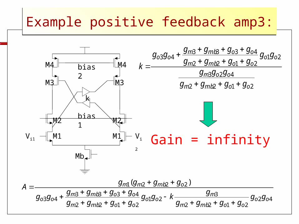
Example positive feedback amp3:Example positive feedback amp3:
2122
423
212122
433343
oombm
oom
oooombm
oombmoo
gggg
ggg
gggggg
gggggg
k
Gain = infinity
Analog and Mixed-Signal VLSI Design Center
IOWA STATE UNIVERSITY22
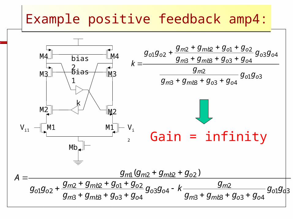
M2
M1
M4
Mb
M1
M3 M3
k
Vi1 Vi2
M2
M4
bias1
bias2
314333
243
4333
212221
2221 )(
oooombm
moo
oombm
oombmoo
ombmm
gggggg
gkgg
gggg
gggggg
ggggA
Example positive feedback amp4:Example positive feedback amp4:
314333
2
434333
212221
oooombm
m
oooombm
oombmoo
gggggg
g
gggggg
gggggg
k
Gain = infinity
Analog and Mixed-Signal VLSI Design Center
IOWA STATE UNIVERSITY23
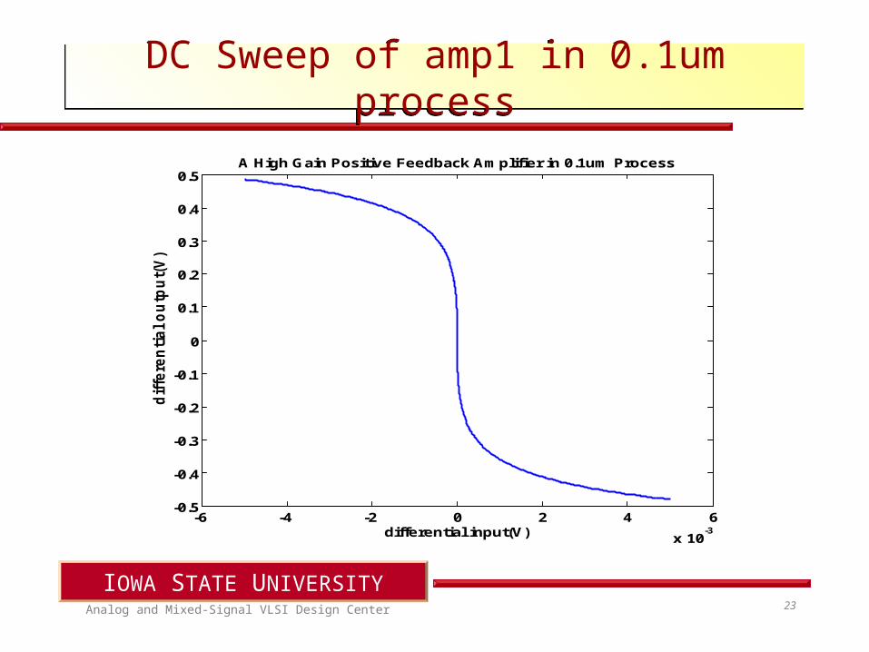
DC Sweep of amp1 in 0.1um processDC Sweep of amp1 in 0.1um process
-6 -4 -2 0 2 4 6
x 10-3
-0.5
-0.4
-0.3
-0.2
-0.1
0
0.1
0.2
0.3
0.4
0.5
differential input(V)
dif
fere
nti
al
ou
tpu
t(V
)A High Gain Positive Feedback Amplifier in 0.1um Process
Analog and Mixed-Signal VLSI Design Center
IOWA STATE UNIVERSITY24
Preliminary Results: DBISTSC PFAmpPreliminary Results: DBISTSC PFAmp
A Digital Programmable Amplifier
Bifurcation in Positive Feedback Amplifier
Simulation and Measurement Results
Analog and Mixed-Signal VLSI Design Center
IOWA STATE UNIVERSITY25
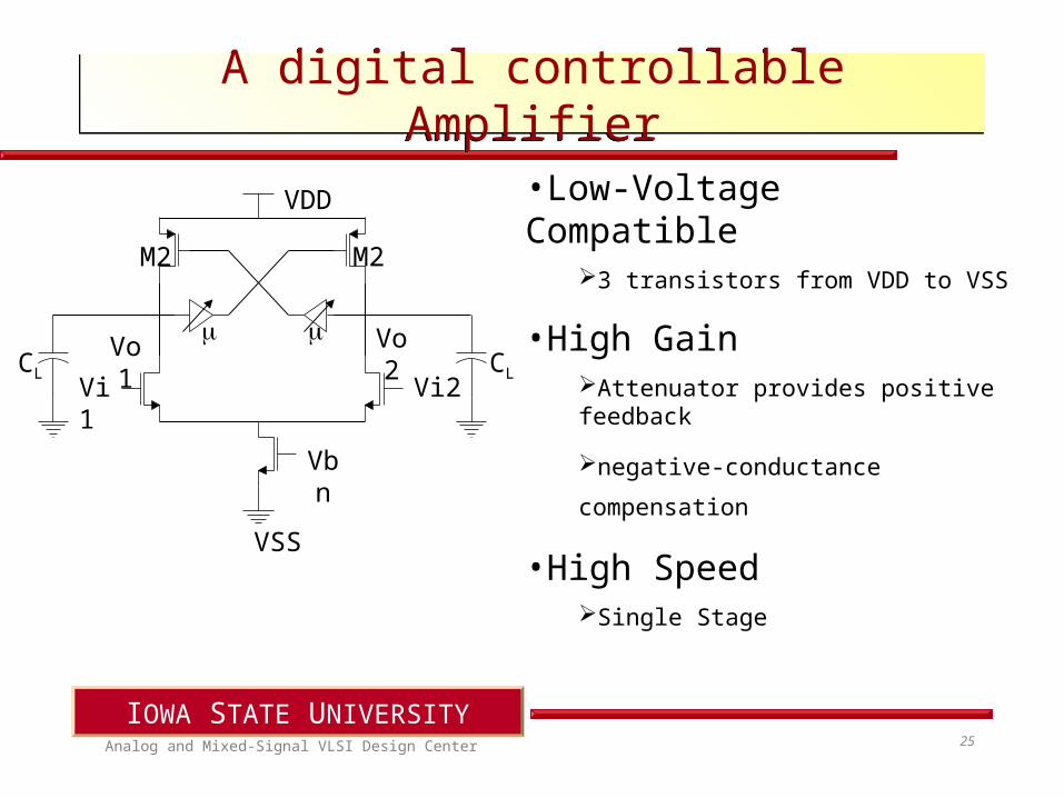
A digital controllable AmplifierA digital controllable Amplifier
•Low-Voltage Compatible3 transistors from VDD to VSS
•High GainAttenuator provides positive feedback
negative-conductance
compensation
•High SpeedSingle Stage
M2 M2
Vi1
Vi2
Vbn
Vo1 Vo2 CL CL
VDD
VSS
Analog and Mixed-Signal VLSI Design Center
IOWA STATE UNIVERSITY26
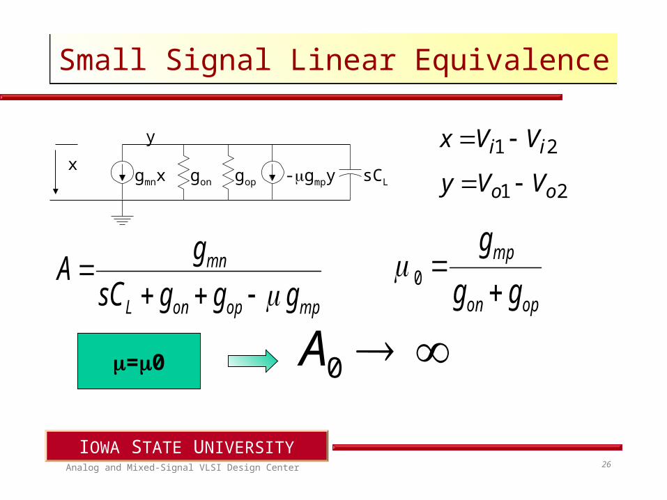
Small Signal Linear EquivalenceSmall Signal Linear Equivalence
21 ii VVx
21 oo VVy gopgongmnx
y
xsCL-gmpy
0A=0
opon
mp
gg
g
0
mpoponL
mn
gggsC
gA
Analog and Mixed-Signal VLSI Design Center
IOWA STATE UNIVERSITY27
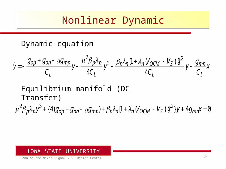
Nonlinear DynamicNonlinear Dynamic
04})](1[)(4{ 232 xgyxVVgggy mnSOCMnnnmponoppp
xC
gy
C
xVVy
Cy
C
gggy
L
mn
L
SOCMnnn
L
pp
L
mponop
4
)](1[
4
23
2
Dynamic equation
Equilibrium manifold (DC Transfer)
Analog and Mixed-Signal VLSI Design Center
IOWA STATE UNIVERSITY28
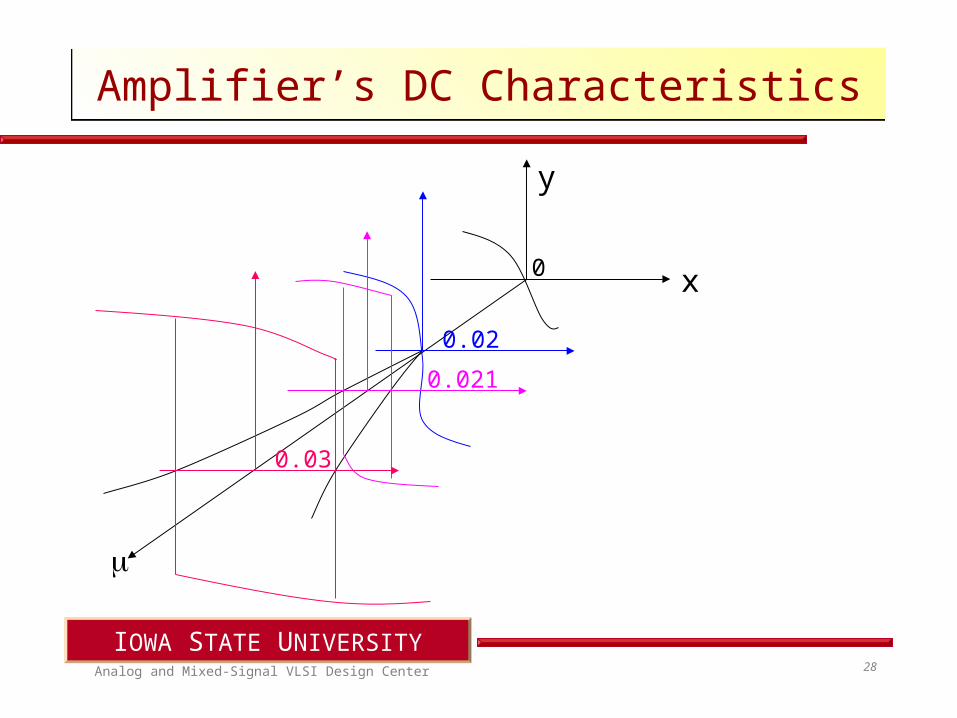
Amplifier’s DC CharacteristicsAmplifier’s DC Characteristics
x
y
0
0.02
0.021
0.03
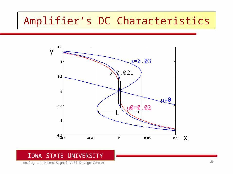
Analog and Mixed-Signal VLSI Design Center
IOWA STATE UNIVERSITY29
y
-0.1 -0.05 0 0.05 0.1-1.5
-1
-0.5
0
0.5
1
1.5
x
y
0=0.02=0
=0.021
=0.03
L
Amplifier’s DC CharacteristicsAmplifier’s DC Characteristics
Analog and Mixed-Signal VLSI Design Center
IOWA STATE UNIVERSITY30
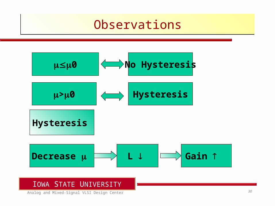
0
>0 Hysteresis
No Hysteresis
Decrease L Gain
Hysteresis
ObservationsObservations
Analog and Mixed-Signal VLSI Design Center
IOWA STATE UNIVERSITY31
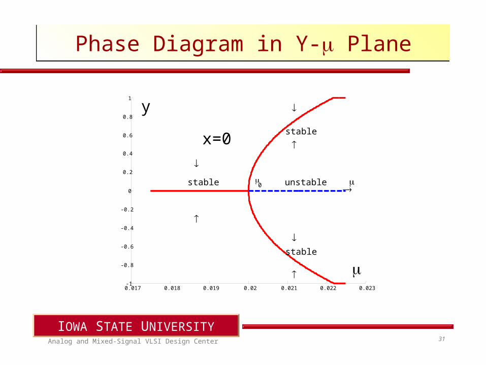
Phase Diagram in Y- PlanePhase Diagram in Y- Plane
0.017 0.018 0.019 0.02 0.021 0.022 0.023-1
-0.8
-0.6
-0.4
-0.2
0
0.2
0.4
0.6
0.8
1
0
unstable
stable
stable
stable
y
x=0
Analog and Mixed-Signal VLSI Design Center
IOWA STATE UNIVERSITY32
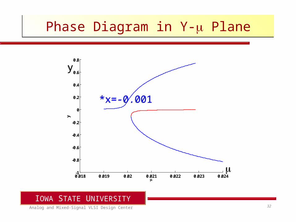
Phase Diagram in Y- PlanePhase Diagram in Y- Plane
0.018 0.019 0.02 0.021 0.022 0.023 0.024-1
-0.8
-0.6
-0.4
-0.2
0
0.2
0.4
0.6
0.8
y
yy
*x=-0.001*x=-0.001
Analog and Mixed-Signal VLSI Design Center
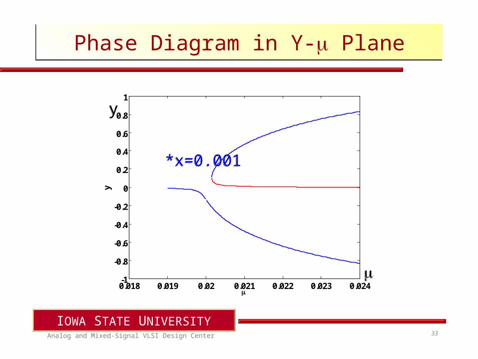
IOWA STATE UNIVERSITY33
Phase Diagram in Y- PlanePhase Diagram in Y- Plane
0.018 0.019 0.02 0.021 0.022 0.023 0.024-1
-0.8
-0.6
-0.4
-0.2
0
0.2
0.4
0.6
0.8
1
yyy
*x=0.001*x=0.001
Analog and Mixed-Signal VLSI Design Center
IOWA STATE UNIVERSITY34
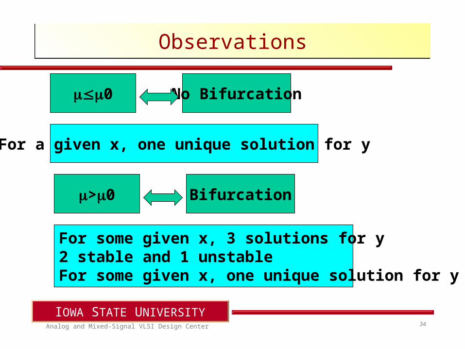
ObservationsObservations
>0 Bifurcation
For some given x, 3 solutions for y2 stable and 1 unstableFor some given x, one unique solution for y
0 No Bifurcation
For a given x, one unique solution for y
Analog and Mixed-Signal VLSI Design Center
IOWA STATE UNIVERSITY35
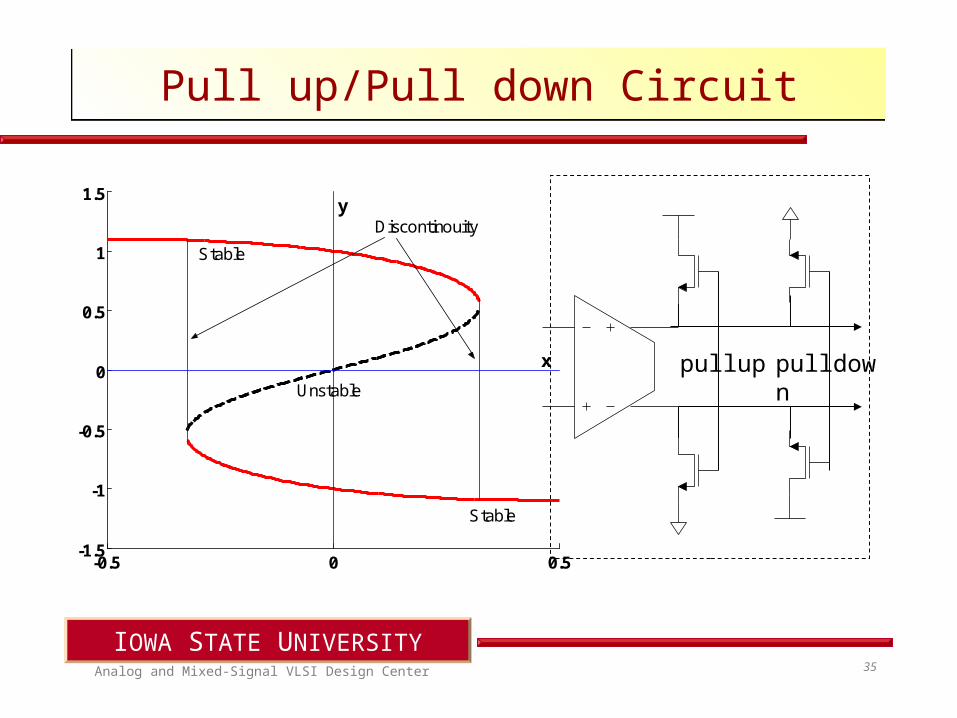
Pull up/Pull down CircuitPull up/Pull down Circuit
-0.5 0 0.5-1.5
-1
-0.5
0
0.5
1
1.5
x
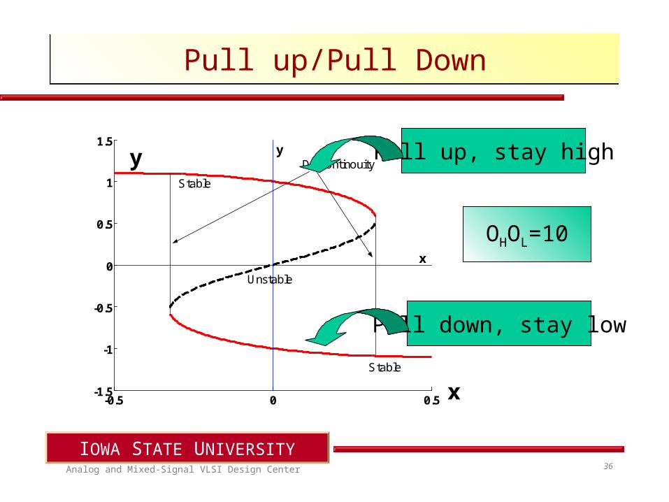
yDiscontinouity
Stable
Unstable
Stable
pullup pulldown
Analog and Mixed-Signal VLSI Design Center
IOWA STATE UNIVERSITY36
-0.5 0 0.5-1.5
-1
-0.5
0
0.5
1
1.5
x
yDiscontinouity
Stable
Unstable
Stable
x
Pull down, stay low
OHOL=10
y
Pull up/Pull DownPull up/Pull Down
Pull up, stay high
Analog and Mixed-Signal VLSI Design Center
IOWA STATE UNIVERSITY37
-0.5 0 0.5-1.5
-1
-0.5
0
0.5
1
1.5
x
yDiscontinouity
Stable
Unstable
Stable
x
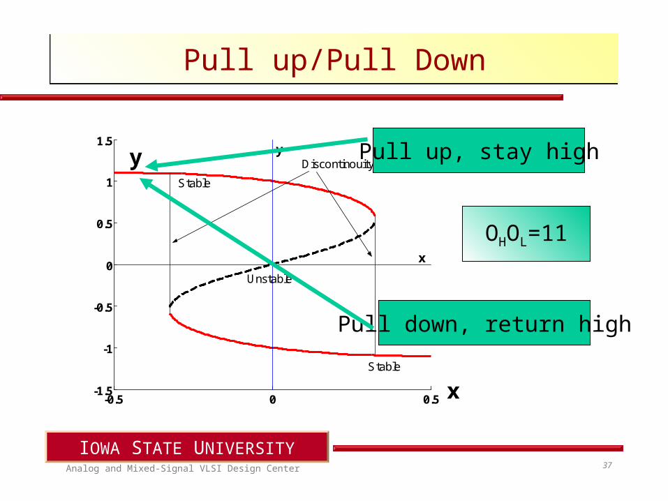
Pull down, return high
OHOL=11
y
Pull up/Pull DownPull up/Pull Down
Pull up, stay high
Analog and Mixed-Signal VLSI Design Center
IOWA STATE UNIVERSITY38
-0.5 0 0.5-1.5
-1
-0.5
0
0.5
1
1.5
x
yDiscontinouity
Stable
Unstable
Stable
x
Pull down, stay low
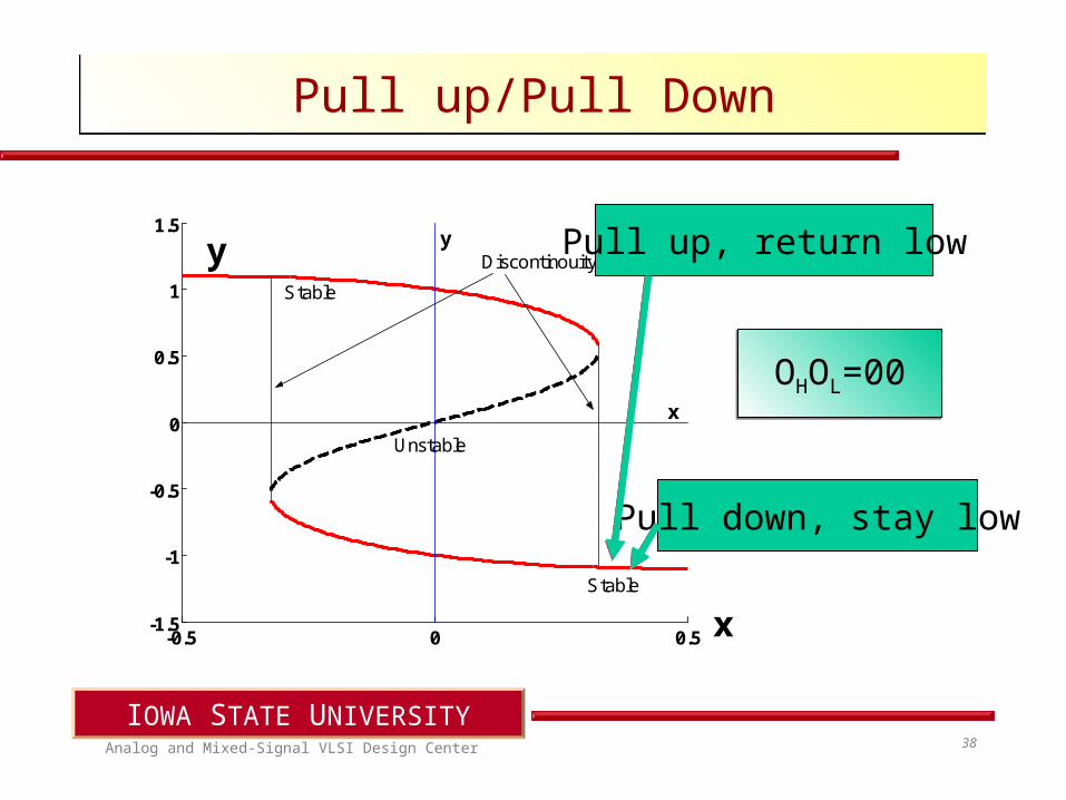
OHOL=00OHOL=00
y
Pull up/Pull DownPull up/Pull Down
Pull up, return low
Analog and Mixed-Signal VLSI Design Center
IOWA STATE UNIVERSITY39
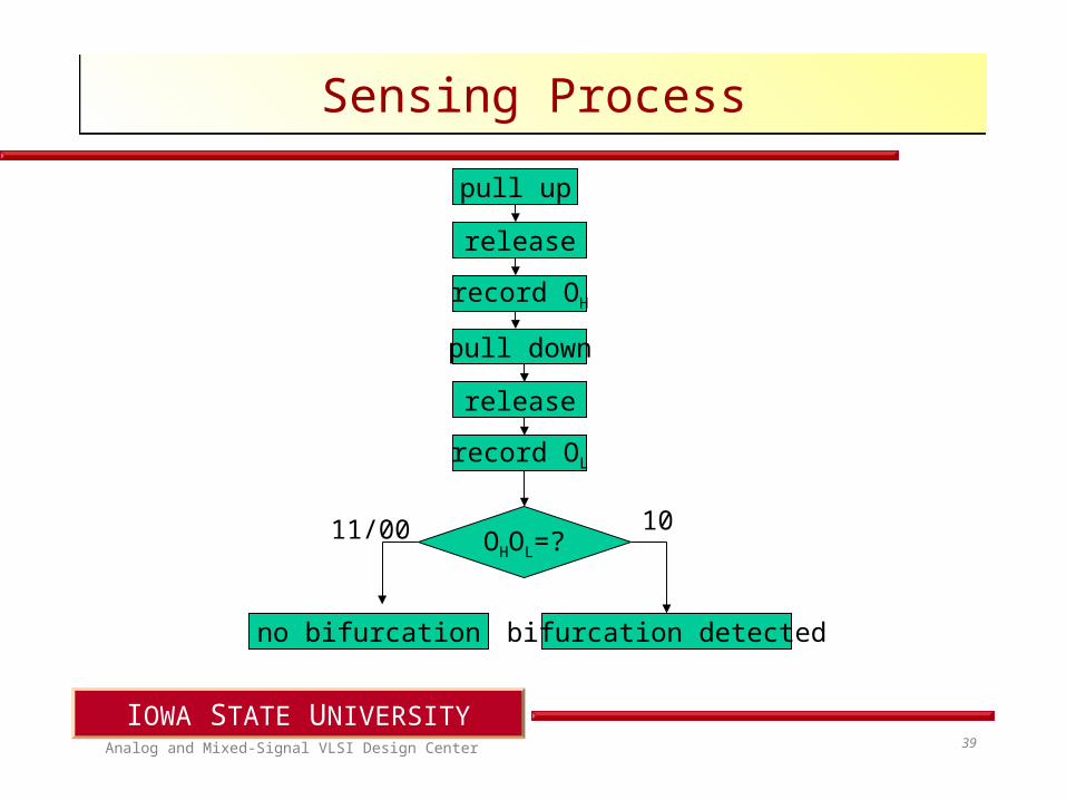
Sensing ProcessSensing Process
pull up
release
record OH
pull down
release
record OL
OHOL=?
no bifurcation bifurcation detected
11/00 10
Analog and Mixed-Signal VLSI Design Center
IOWA STATE UNIVERSITY40
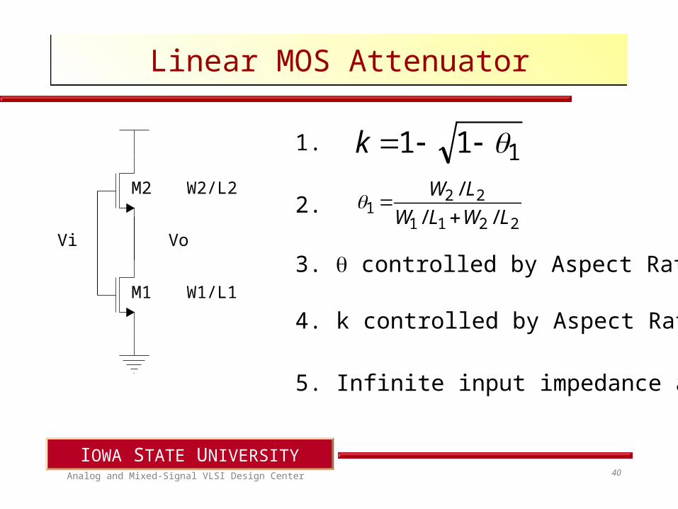
Linear MOS AttenuatorLinear MOS Attenuator
111 k1.
3. controlled by Aspect Ratio Vo
M2
M1
Vi
W2/L2
W1/L1
2211
221 //
/
LWLW
LW
2.
4. k controlled by Aspect Ratio
5. Infinite input impedance at DC
Analog and Mixed-Signal VLSI Design Center
IOWA STATE UNIVERSITY41
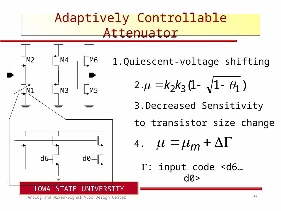
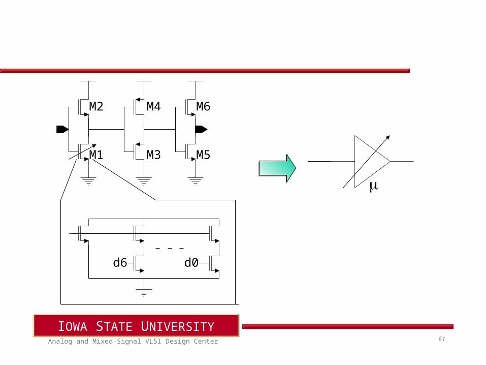
Adaptively Controllable AttenuatorAdaptively Controllable Attenuator
M2
M1
M4
M3
M6
M5
d6 d0
1.Quiescent-voltage shifting
)11( 132 kk2.
3.Decreased Sensitivity
to transistor size change
m4.
: input code <d6…d0>
Analog and Mixed-Signal VLSI Design Center
IOWA STATE UNIVERSITY42
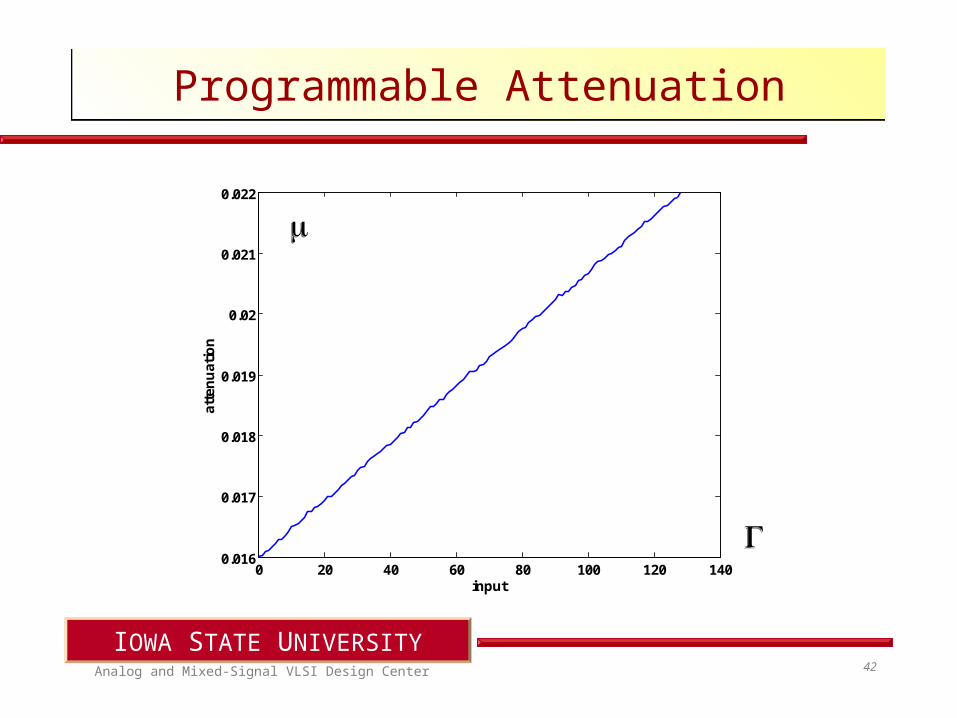
Programmable AttenuationProgrammable Attenuation
0 20 40 60 80 100 120 1400.016
0.017
0.018
0.019
0.02
0.021
0.022
input
atte
nu
atio
n
Analog and Mixed-Signal VLSI Design Center
IOWA STATE UNIVERSITY43
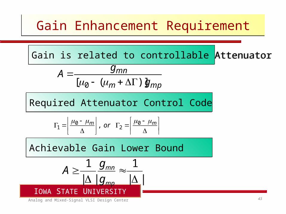
Gain Enhancement RequirementGain Enhancement Requirement
mpm
mn
g
gA
)]([ 0
||
1
||
1
mp
mn
g
gA
Gain is related to controllable AttenuatorGain is related to controllable Attenuator
Required Attenuator Control CodeRequired Attenuator Control Code
Achievable Gain Lower BoundAchievable Gain Lower Bound
mm or 0
20
1 ,
Analog and Mixed-Signal VLSI Design Center
IOWA STATE UNIVERSITY44
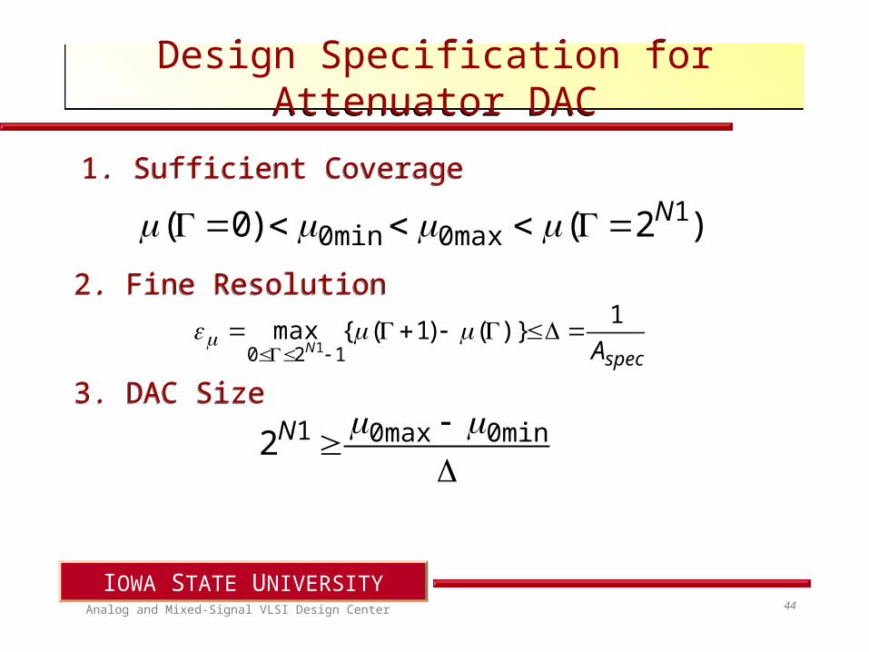
Design Specification for Attenuator DAC
Design Specification for Attenuator DAC
1. Sufficient Coverage1. Sufficient Coverage
)2()0( 1max0min0
N
2. Fine Resolution2. Fine Resolution
specAN
1)}()1({max
120 1
3. DAC Size3. DAC Size
min0max012N
Analog and Mixed-Signal VLSI Design Center
IOWA STATE UNIVERSITY45
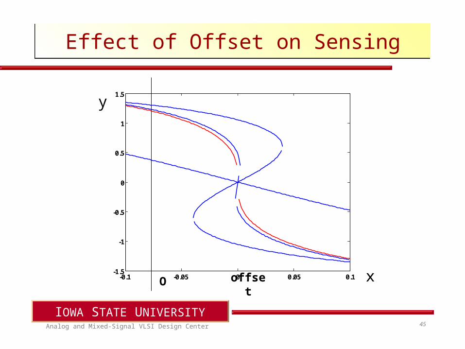
Effect of Offset on SensingEffect of Offset on Sensing
-0.1 -0.05 0 0.05 0.1-1.5
-1
-0.5
0
0.5
1
1.5
x
y
offset
O
Analog and Mixed-Signal VLSI Design Center
IOWA STATE UNIVERSITY46
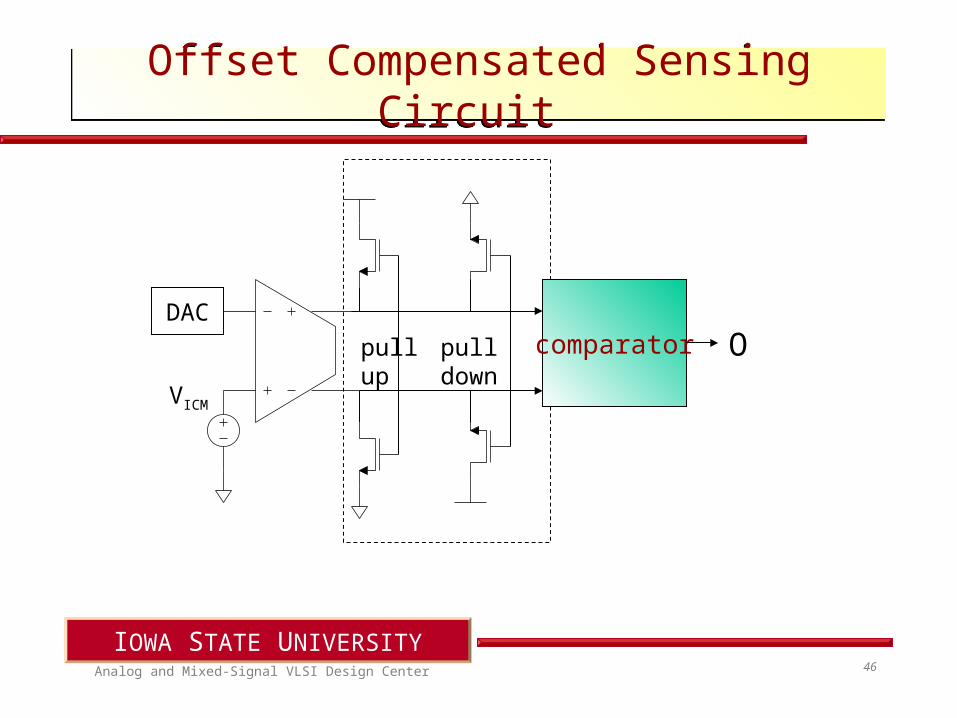
Offset Compensated Sensing Circuit Offset Compensated Sensing Circuit
pull up pull down
VICM
DACcomparator O
Analog and Mixed-Signal VLSI Design Center
IOWA STATE UNIVERSITY47
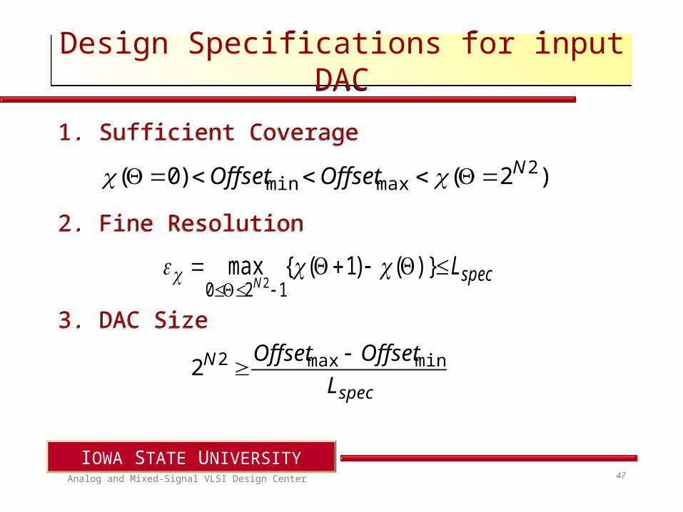
Design Specifications for input DACDesign Specifications for input DAC
1. Sufficient Coverage1. Sufficient Coverage
)2()0( 2maxmin
NOffsetOffset
2. Fine Resolution2. Fine Resolution
specLN
)}()1({max120 2
3. DAC Size3. DAC Size
spec
N
L
OffsetOffset minmax22
Analog and Mixed-Signal VLSI Design Center
IOWA STATE UNIVERSITY48
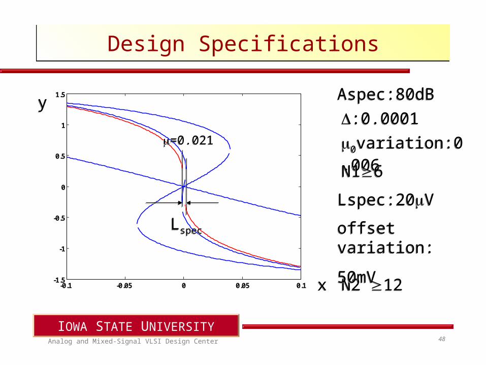
Design SpecificationsDesign Specifications
y
-0.1 -0.05 0 0.05 0.1-1.5
-1
-0.5
0
0.5
1
1.5
xx
yy
=0.021=0.021
LspecLspec
Aspec:80dBAspec:80dB
Lspec:20VLspec:20V
N2 12N2 12
:0.0001:0.0001
offset variation:
50mV
offset variation:
50mV
0variation:0.0060variation:0.006N16N16
Analog and Mixed-Signal VLSI Design Center
IOWA STATE UNIVERSITY49
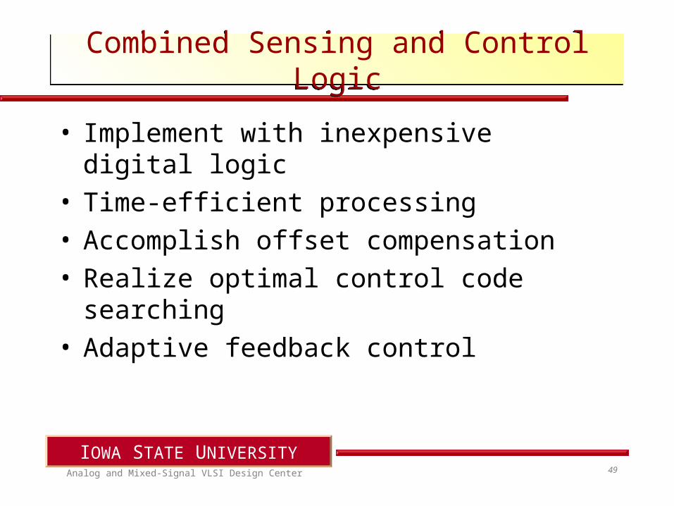
Combined Sensing and Control LogicCombined Sensing and Control Logic
• Implement with inexpensive digital logic• Time-efficient processing• Accomplish offset compensation• Realize optimal control code searching• Adaptive feedback control
Analog and Mixed-Signal VLSI Design Center
IOWA STATE UNIVERSITY50
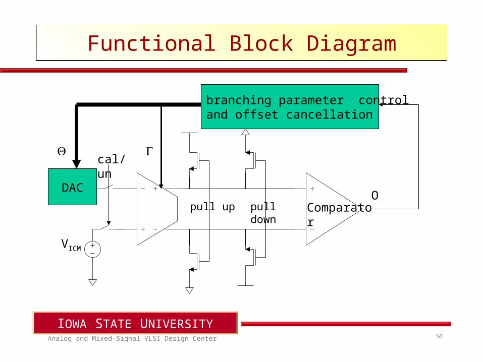
Functional Block DiagramFunctional Block Diagram
pull up pull down
VICM
ComparatorO
branching parameter controland offset cancellation
DAC
cal/un
Analog and Mixed-Signal VLSI Design Center
IOWA STATE UNIVERSITY51
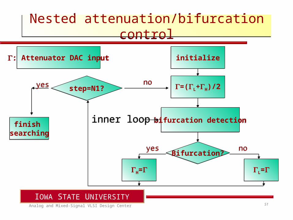
Nested attenuation/bifurcation controlNested attenuation/bifurcation control
initializeinitialize
=(L+H)/2=(L+H)/2
bifurcation detectionbifurcation detection
Bifurcation?Bifurcation?
L=L=H=H=
nono
: Attenuator DAC input: Attenuator DAC input
yesyes nono
step=N1?step=N1?yesyes
finish searching
finish searching
inner loopinner loop
Analog and Mixed-Signal VLSI Design Center
IOWA STATE UNIVERSITY52
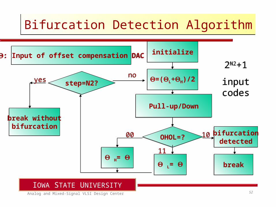
Bifurcation Detection AlgorithmBifurcation Detection Algorithm
initializeinitialize
=(L+H)/2=(L+H)/2
Pull-up/DownPull-up/Down
OHOL=?OHOL=? bifurcationdetected
bifurcationdetected
H= H=
: Input of offset compensation DAC: Input of offset compensation DAC
0000 1010
breakbreak L= L=
1111
nono2N2+1
input codes
2N2+1
input codes
step=N2?step=N2?yesyes
break withoutbifurcation
break withoutbifurcation
Analog and Mixed-Signal VLSI Design Center
IOWA STATE UNIVERSITY53
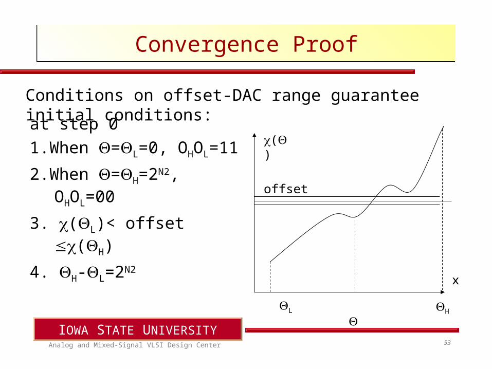
Convergence ProofConvergence Proof
Conditions on offset-DAC range guarantee initial conditions:
H
()
x
offset
L
at step 01.When =L=0, OHOL=11
2.When =H=2N2, OHOL=00
3. (L)< offset (H)
4. H-L=2N2
Analog and Mixed-Signal VLSI Design Center
IOWA STATE UNIVERSITY54
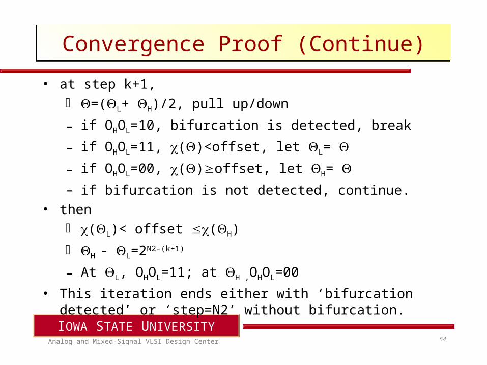
Convergence Proof (Continue)Convergence Proof (Continue)
• at step k+1, =(L+ H)/2, pull up/down
– if OHOL=10, bifurcation is detected, break
– if OHOL=11, ()<offset, let L=
– if OHOL=00, ()offset, let H=
– if bifurcation is not detected, continue.
• then (L)< offset (H)
H - L=2N2-(k+1)
– At L, OHOL=11; at H ,OHOL=00
• This iteration ends either with ‘bifurcation detected’ or ‘step=N2’ without bifurcation.
Analog and Mixed-Signal VLSI Design Center
IOWA STATE UNIVERSITY55
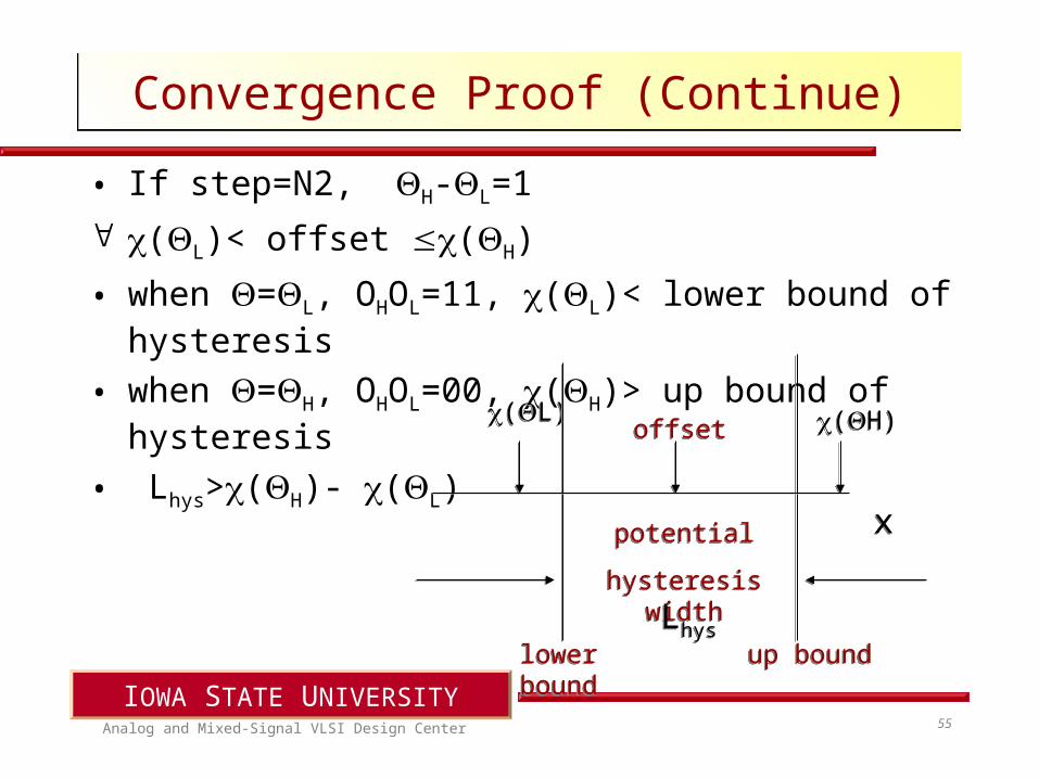
Convergence Proof (Continue)Convergence Proof (Continue)
• If step=N2, H-L=1
(L)< offset (H)
• when =L, OHOL=11, (L)< lower bound of hysteresis
• when =H, OHOL=00, (H)> up bound of hysteresis
• Lhys>(H)- (L)offsetoffset
(L)(L) (H)(H)
potential
hysteresis width
potential
hysteresis width
xx
lower boundlower bound up boundup boundLhysLhys
Analog and Mixed-Signal VLSI Design Center
IOWA STATE UNIVERSITY56
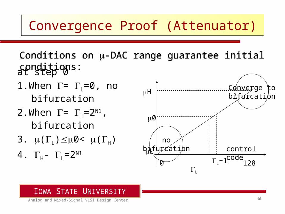
Convergence Proof (Attenuator)Convergence Proof (Attenuator)
L
H
0 128
control code
Converge tobifurcation
nobifurcation
0
L L+1
Conditions on -DAC range guarantee initial conditions:Conditions on -DAC range guarantee initial conditions:at step 0
1.When = L=0, no bifurcation
2.When = H=2N1, bifurcation
3. (L)0< (H)
4. H- L=2N1
Analog and Mixed-Signal VLSI Design Center
IOWA STATE UNIVERSITY57
Convergence Proof (Attenuator)Convergence Proof (Attenuator)
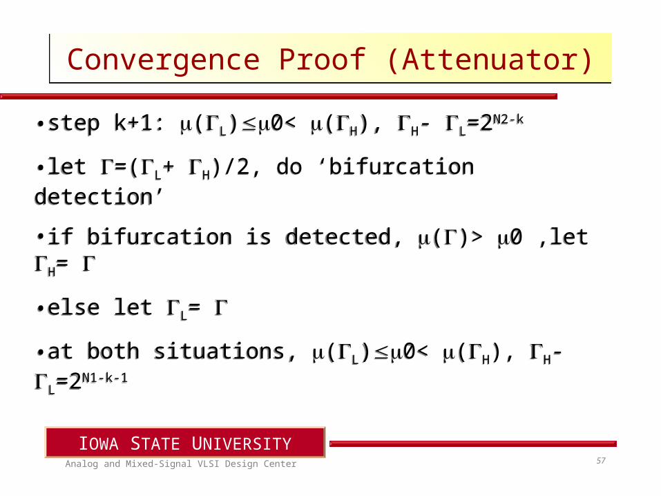
•step k+1: (L)0< (H), H- L=2N2-k
•let =(L+ H)/2, do ‘bifurcation detection’
•if bifurcation is detected, ()> 0 ,let H=
•else let L=
•at both situations, (L)0< (H), H- L=2N1-k-1
•step k+1: (L)0< (H), H- L=2N2-k
•let =(L+ H)/2, do ‘bifurcation detection’
•if bifurcation is detected, ()> 0 ,let H=
•else let L=
•at both situations, (L)0< (H), H- L=2N1-k-1
Analog and Mixed-Signal VLSI Design Center
IOWA STATE UNIVERSITY58
Convergence Proof (Attenuator)Convergence Proof (Attenuator)
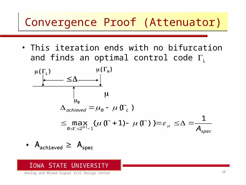
• This iteration ends with no bifurcation and finds an optimal control code L
spec
Lachieved
AN
1)}()1({max
)(
120
0
1
• Aachieved Aspec• Aachieved Aspec
(L)(L) (H)(H)
00
Analog and Mixed-Signal VLSI Design Center
IOWA STATE UNIVERSITY59
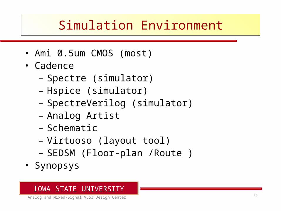
Simulation EnvironmentSimulation Environment
• Ami 0.5um CMOS (most)• Cadence
– Spectre (simulator)– Hspice (simulator)– SpectreVerilog (simulator)– Analog Artist– Schematic– Virtuoso (layout tool)– SEDSM (Floor-plan /Route )
• Synopsys
Analog and Mixed-Signal VLSI Design Center
IOWA STATE UNIVERSITY60
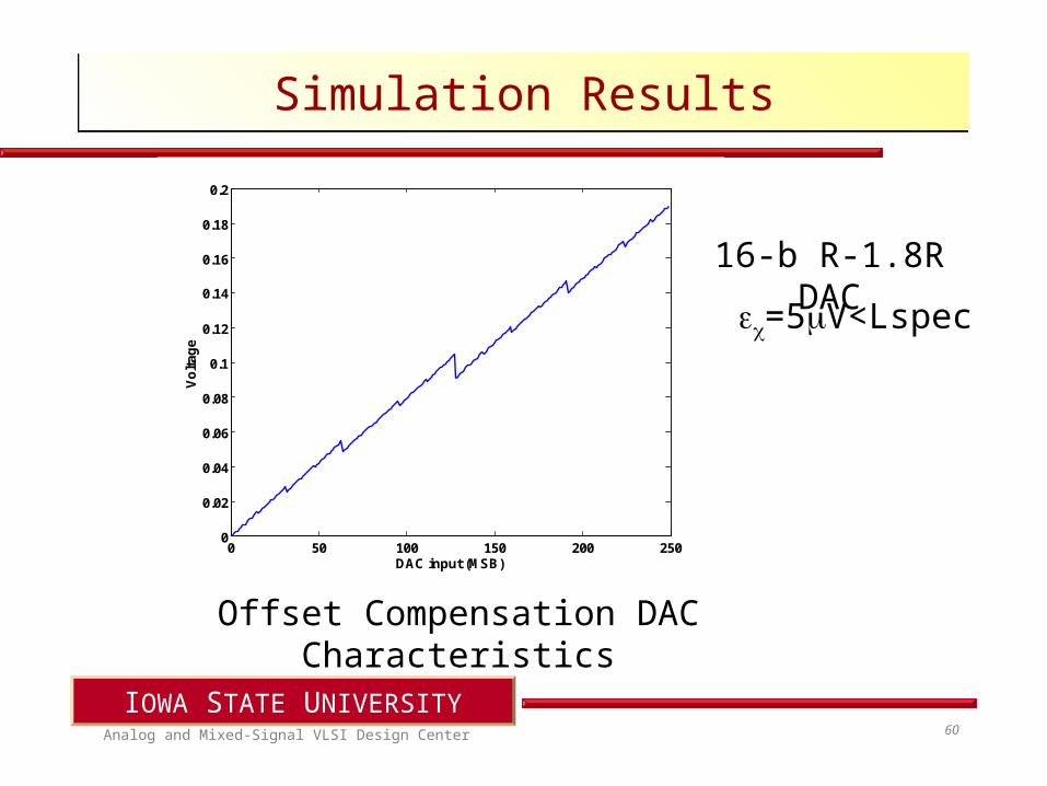
Simulation ResultsSimulation Results
0 50 100 150 200 2500
0.02
0.04
0.06
0.08
0.1
0.12
0.14
0.16
0.18
0.2
DAC input (MSB)
Vo
ltag
e
Offset Compensation DAC Characteristics
16-b R-1.8R DAC=5V<Lspe
c
Analog and Mixed-Signal VLSI Design Center
IOWA STATE UNIVERSITY61
M2
M1
M4
M3
M6
M5
d6 d0
Analog and Mixed-Signal VLSI Design Center
IOWA STATE UNIVERSITY62
Digitally controlled PF AmplifierDigitally controlled PF Amplifier
+ -
cmfb
- +
VDD
VSS
+
-
-
+
A1
+ -
cmfb
- +
VDD
VSS
Vbp
+
-
-
+A2
Analog and Mixed-Signal VLSI Design Center
IOWA STATE UNIVERSITY63
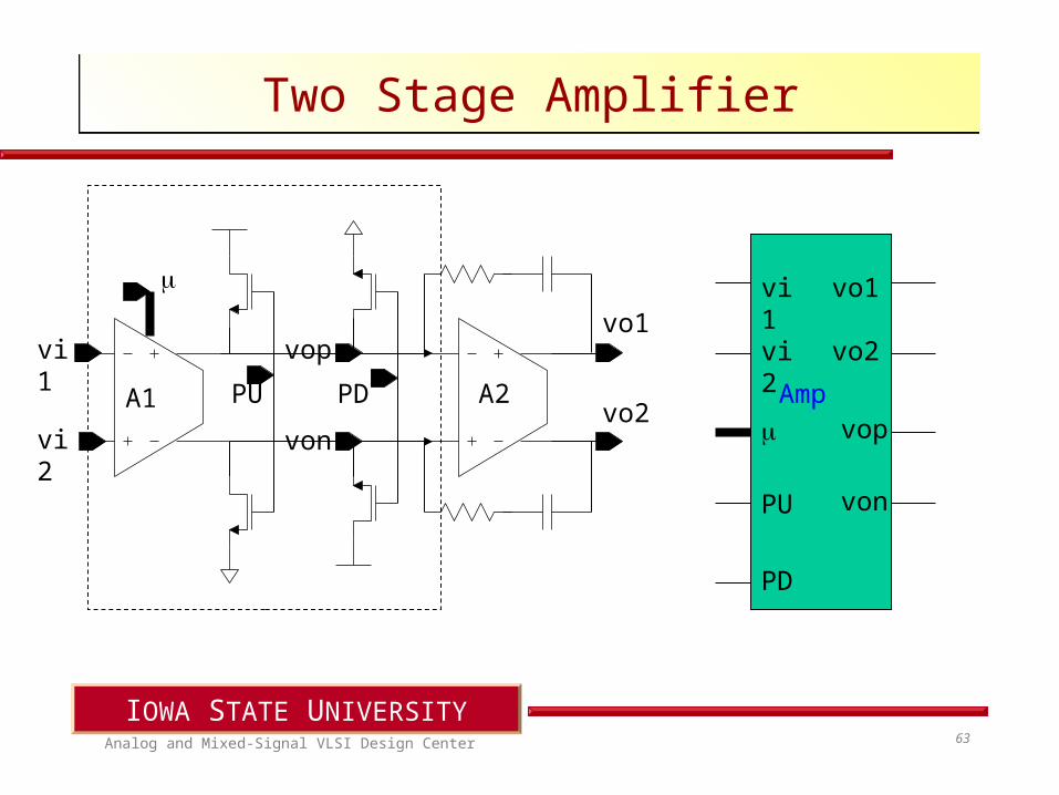
Two Stage AmplifierTwo Stage Amplifier
PU PDA1 A2
vi1
vi2
vop
von
vo1
vo2
vi1
vi2
PU
PD
vo1
vo2
vop
von
Amp
Analog and Mixed-Signal VLSI Design Center
IOWA STATE UNIVERSITY64
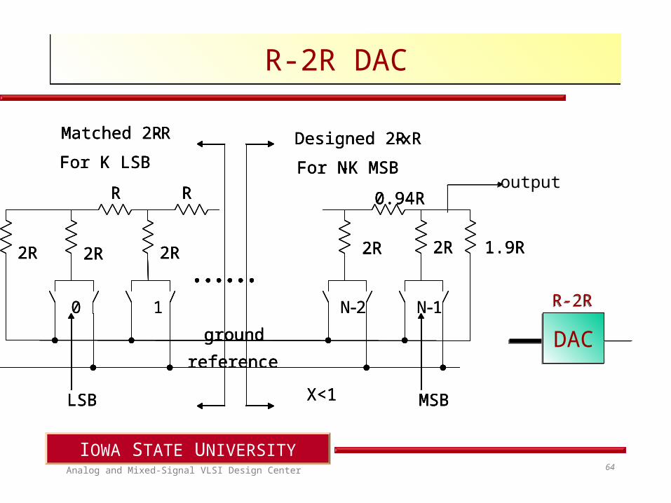
R-2R DACR-2R DAC
DACDAC
R-2RR-2R
ground
reference
2R 2R 2R 2R 2R 1.9R
R R 0.94R
Matched 2R-R
For K LSB
Designed 2R-xR
For N-K MSB
X<1LSB MSB
0 1 N-2 N-1
ground
reference
2R 2R 2R 2R 2R 1.9R
R R 0.94R
Matched 2R-R
For K LSB
Designed 2R-xR
For N-K MSB
X<1
ground
reference
2R 2R 2R 2R 2R 1.9R
R R 0.94R
ground
reference
2R 2R 2R 2R 2R 1.9R
R R 0.94R
Matched 2R-R
For K LSB
Designed 2R-xR
For N-K MSB
X<1
output
LSBLSB MSBMSB
0 1 N-2 N-1
Analog and Mixed-Signal VLSI Design Center
IOWA STATE UNIVERSITY65
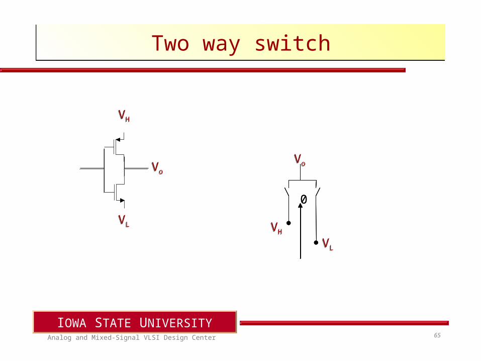
Two way switchTwo way switch
00
VHVHVLVL
VoVo
VoVo
VHVH
VLVL
Analog and Mixed-Signal VLSI Design Center
IOWA STATE UNIVERSITY66
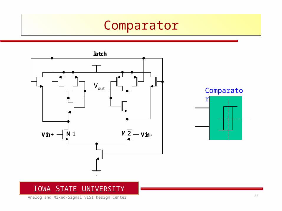
ComparatorComparator
Vin+ Vin-
latch
M1 M2Vin+ Vin-
latch
Vin+ Vin-
latch
M1 M2
Vout Comparator
Analog and Mixed-Signal VLSI Design Center
IOWA STATE UNIVERSITY67
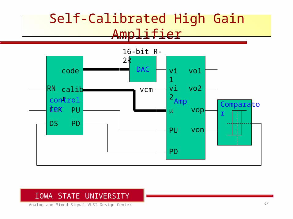
Self-Calibrated High Gain AmplifierSelf-Calibrated High Gain Amplifier
vi1
vi2
PU
PD
vo1
vo2
vop
von
DACcode
calibr
PU
PD
vcm
DS
CLK
RN
controller Amp Comparator
16-bit R-2R
Analog and Mixed-Signal VLSI Design Center
IOWA STATE UNIVERSITY68
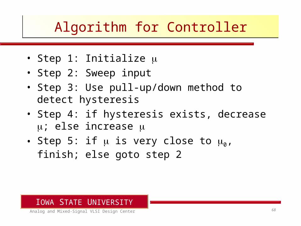
Algorithm for ControllerAlgorithm for Controller
• Step 1: Initialize • Step 2: Sweep input
• Step 3: Use pull-up/down method to detect hysteresis
• Step 4: if hysteresis exists, decrease ; else increase • Step 5: if is very close to 0, finish; else goto step 2
Analog and Mixed-Signal VLSI Design Center
IOWA STATE UNIVERSITY69
Offset Compensation DAC
Attenuator Control DAC
32768 16384 24576 16384 28672 25578 24577
No Bifurcation
64 32 48 52 50 49 48
yesbifurcation: no no yes yes yes
Max searching time: 7x16 cycles
Searching ProcessSearching Process
Analog and Mixed-Signal VLSI Design Center
IOWA STATE UNIVERSITY70
Bifurcation SimulationBifurcation Simulation
pull uppull up
OH=1OH=1
pull downpull down
OL=0OL=0
x=0x=0
Analog and Mixed-Signal VLSI Design Center
IOWA STATE UNIVERSITY71
Pull-up/Pull DownPull-up/Pull Down
pull uppull up
OH=1OH=1
pull downpull down
OL=1OL=1
x=-0.1mV
x=-0.1mV
Analog and Mixed-Signal VLSI Design Center
IOWA STATE UNIVERSITY72
AC Response, single stage onlyAC Response, single stage only
50dB gain enhancement50dB gain enhancement
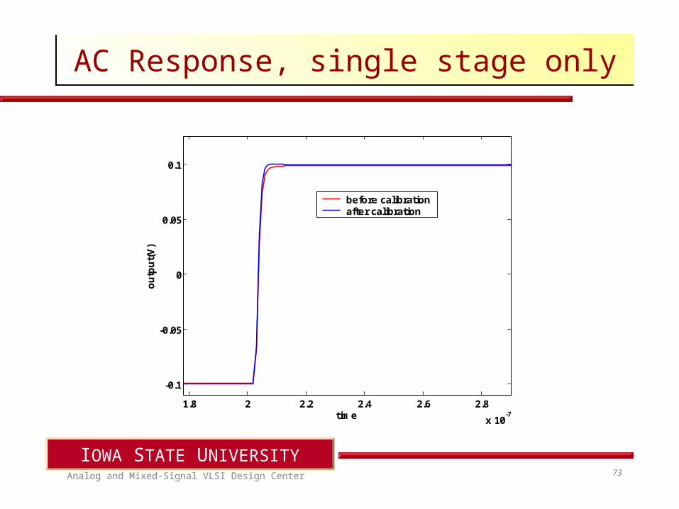
Analog and Mixed-Signal VLSI Design Center
IOWA STATE UNIVERSITY73
1.8 2 2.2 2.4 2.6 2.8
x 10-7
-0.1
-0.05
0
0.05
0.1
time
ou
tpu
t(V
)
before calibrationafter calibration
AC Response, single stage onlyAC Response, single stage only
Analog and Mixed-Signal VLSI Design Center
IOWA STATE UNIVERSITY74
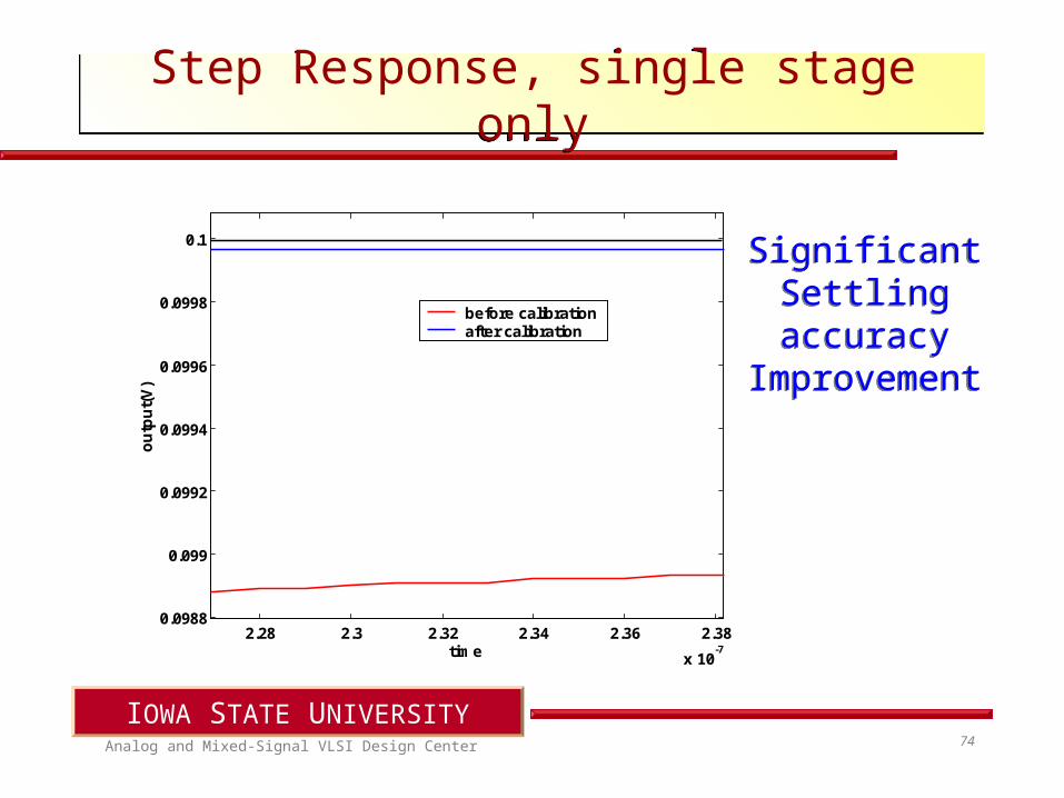
Step Response, single stage onlyStep Response, single stage only
2.28 2.3 2.32 2.34 2.36 2.38
x 10-7
0.0988
0.099
0.0992
0.0994
0.0996
0.0998
0.1
time
ou
tpu
t(V
)
before calibrationafter calibration
Significant Settling
accuracy Improvement
Significant Settling
accuracy Improvement
Analog and Mixed-Signal VLSI Design Center
IOWA STATE UNIVERSITY75
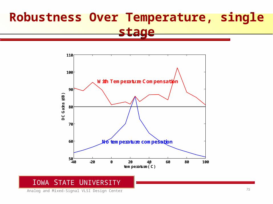
Robustness Over Temperature, single stageRobustness Over Temperature, single stage
-40 -20 0 20 40 60 80 10050
60
70
80
90
100
110
temperature(C)
DC
Gai
ns
(dB
)
No temperature compesation
With Temperature Compensation
Analog and Mixed-Signal VLSI Design Center
IOWA STATE UNIVERSITY76
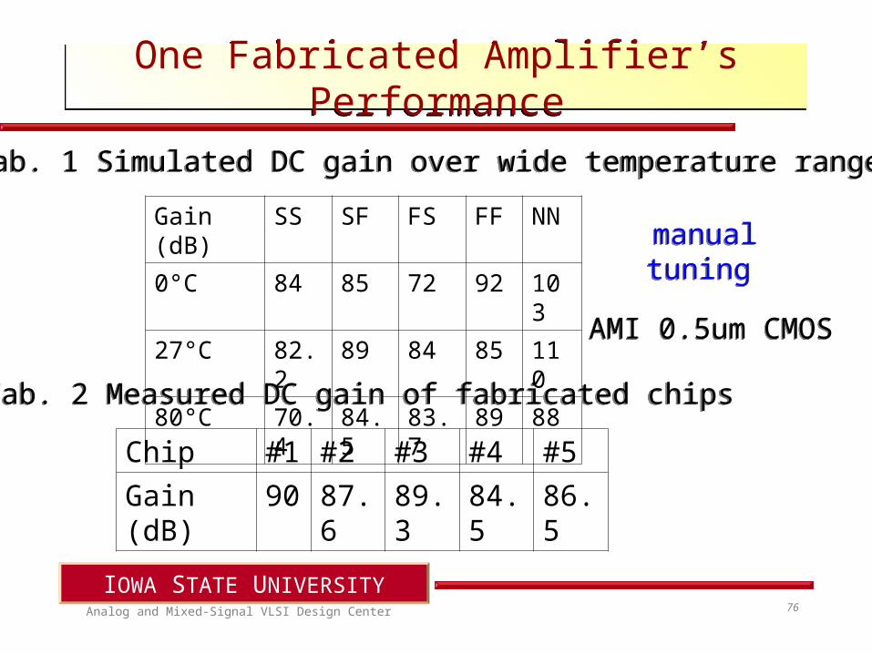
One Fabricated Amplifier’s Performance
One Fabricated Amplifier’s Performance
Tab. 1 Simulated DC gain over wide temperature range Tab. 1 Simulated DC gain over wide temperature range
Gain (dB)
SS SF FS FF NN
0°C 84 85 72 92 103
27°C 82.2
89 84 85 110
80°C 70.4
84.5
83.7
89 88
AMI 0.5um CMOSAMI 0.5um CMOS
Tab. 2 Measured DC gain of fabricated chipsTab. 2 Measured DC gain of fabricated chips
Chip #1
#2 #3 #4 #5
Gain (dB)
90 87.6
89.3
84.5
86.5
manual tuning manual tuning
Analog and Mixed-Signal VLSI Design Center
IOWA STATE UNIVERSITY77
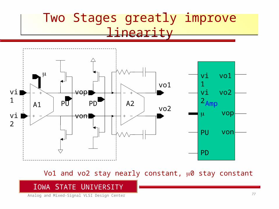
Two Stages greatly improve linearityTwo Stages greatly improve linearity
PU PDA1 A2
vi1
vi2
vop
von
vo1
vo2
vi1
vi2
PU
PD
vo1
vo2
vop
von
Amp
Vo1 and vo2 stay nearly constant, 0 stay constant
Analog and Mixed-Signal VLSI Design Center
IOWA STATE UNIVERSITY78
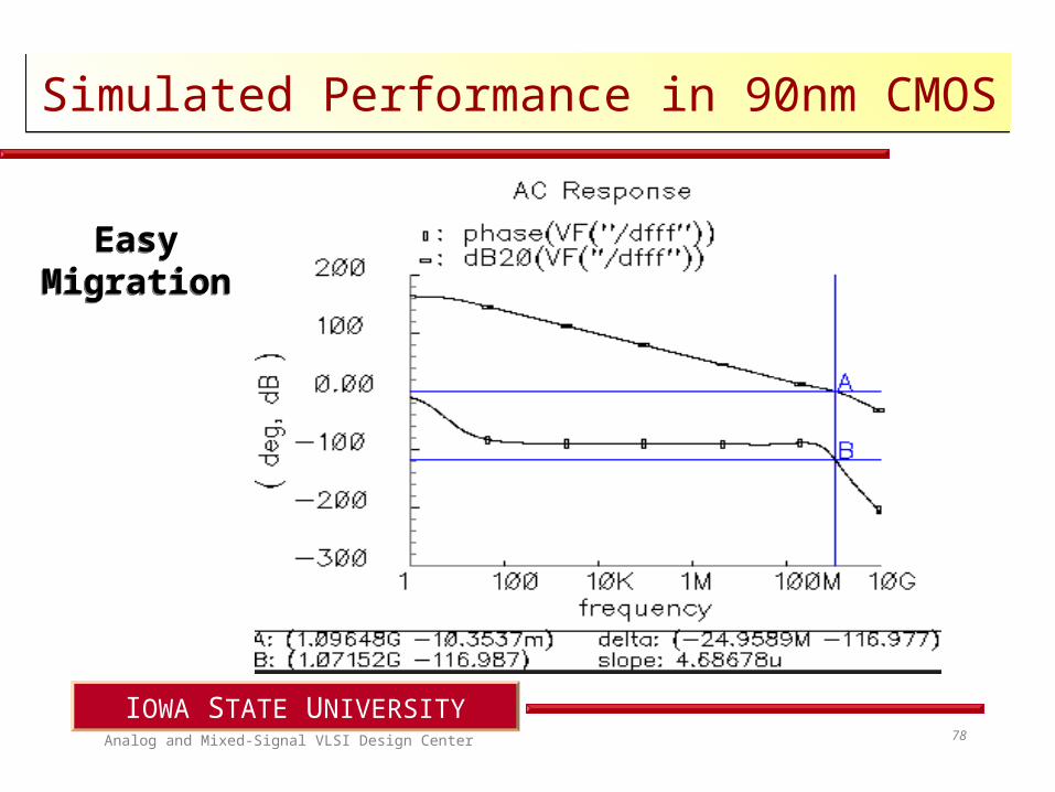
Simulated Performance in 90nm CMOSSimulated Performance in 90nm CMOS
Easy Migration
Easy Migration
Analog and Mixed-Signal VLSI Design Center
IOWA STATE UNIVERSITY79
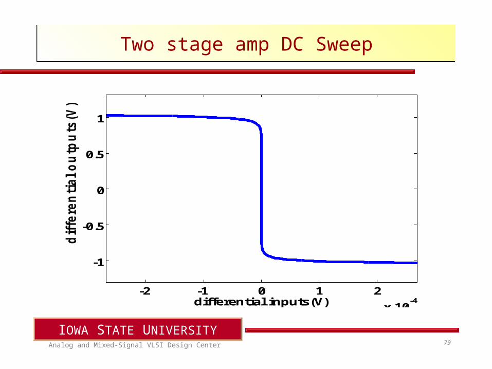
Two stage amp DC SweepTwo stage amp DC Sweep
-2 -1 0 1 2
x 10-4
-1
-0.5
0
0.5
1
differential inputs(V)
dif
fere
nti
al o
utp
uts
(V)
Analog and Mixed-Signal VLSI Design Center
IOWA STATE UNIVERSITY80
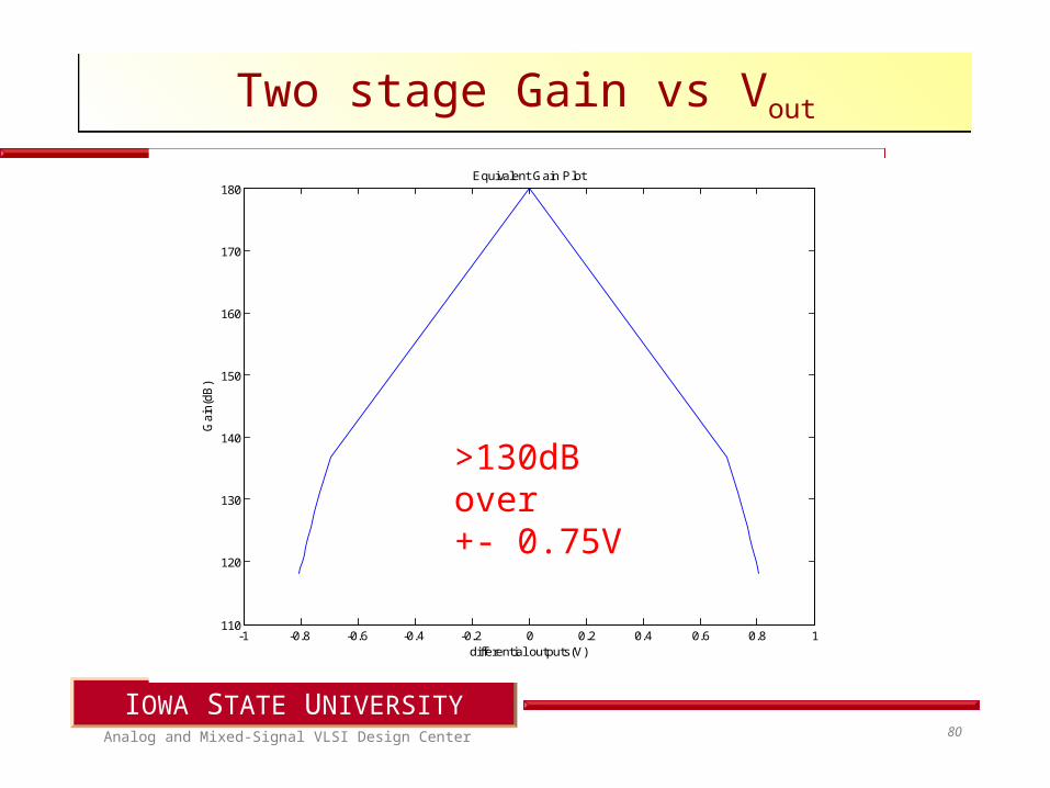
Two stage Gain vs VoutTwo stage Gain vs Vout
-1 -0.8 -0.6 -0.4 -0.2 0 0.2 0.4 0.6 0.8 1110
120
130
140
150
160
170
180
differential outputs(V)
Gai
n(dB
)
Equivalent Gain Plot
>130dBover +- 0.75V
Analog and Mixed-Signal VLSI Design Center
IOWA STATE UNIVERSITY81
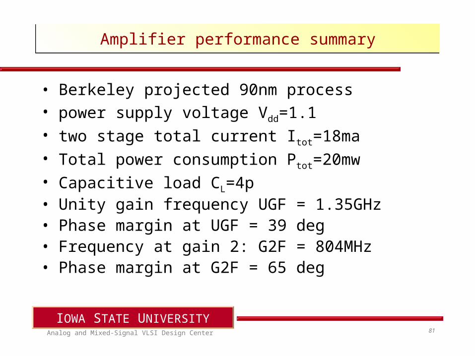
Amplifier performance summaryAmplifier performance summary
• Berkeley projected 90nm process• power supply voltage Vdd=1.1 • two stage total current Itot=18ma• Total power consumption Ptot=20mw• Capacitive load CL=4p • Unity gain frequency UGF = 1.35GHz• Phase margin at UGF = 39 deg• Frequency at gain 2: G2F = 804MHz • Phase margin at G2F = 65 deg
Analog and Mixed-Signal VLSI Design Center
IOWA STATE UNIVERSITY82
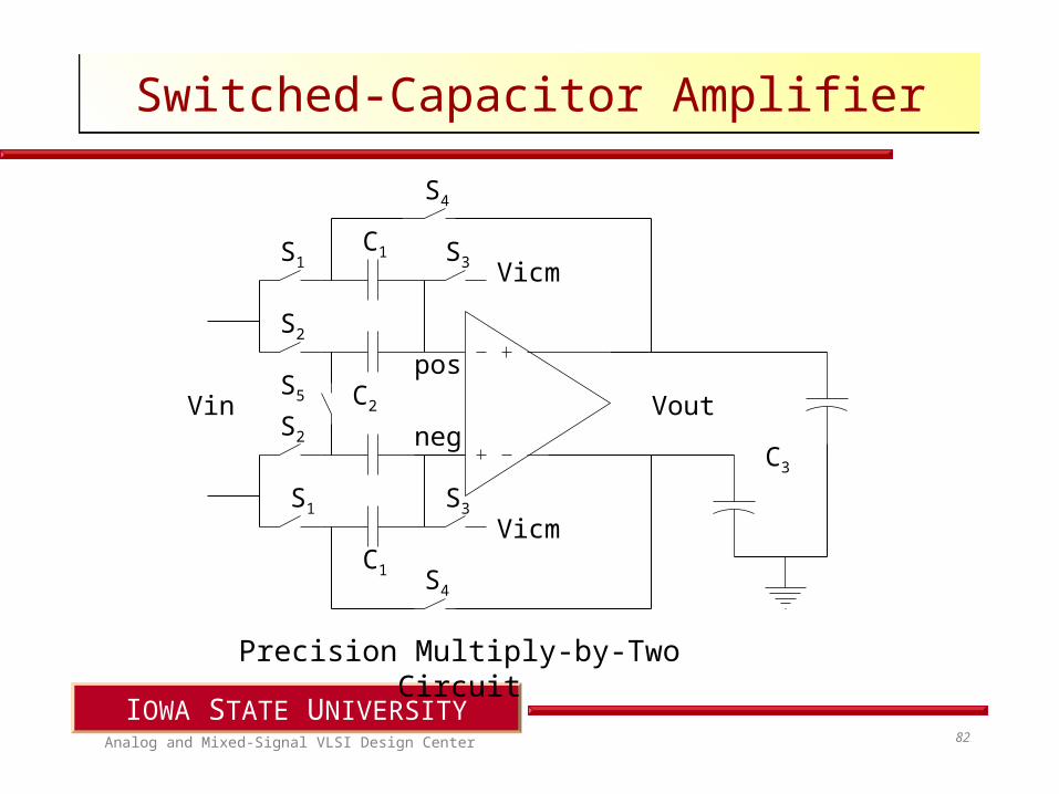
Switched-Capacitor AmplifierSwitched-Capacitor Amplifier
Vout
S1C1
C2
S2
S3
S4
S1
C1
S2
S5Vin
S4
S3
pos
neg
Vicm
Vicm
C3
Precision Multiply-by-Two Circuit
Analog and Mixed-Signal VLSI Design Center
IOWA STATE UNIVERSITY83
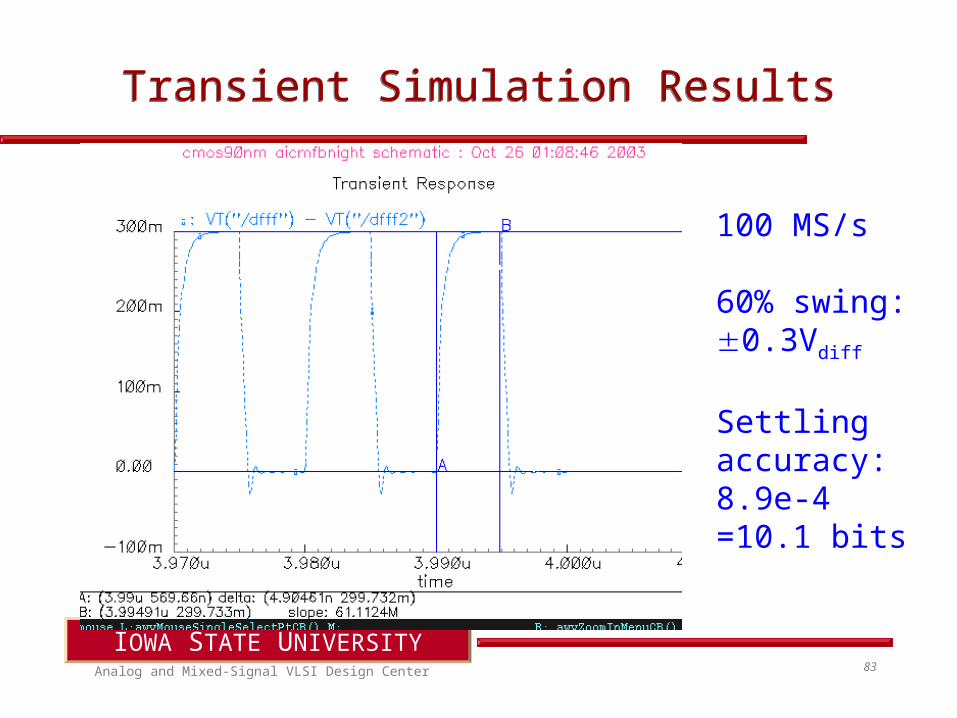
100 MS/s
60% swing:0.3Vdiff
Settlingaccuracy:8.9e-4=10.1 bits
Transient Simulation ResultsTransient Simulation Results
Analog and Mixed-Signal VLSI Design Center
IOWA STATE UNIVERSITY84
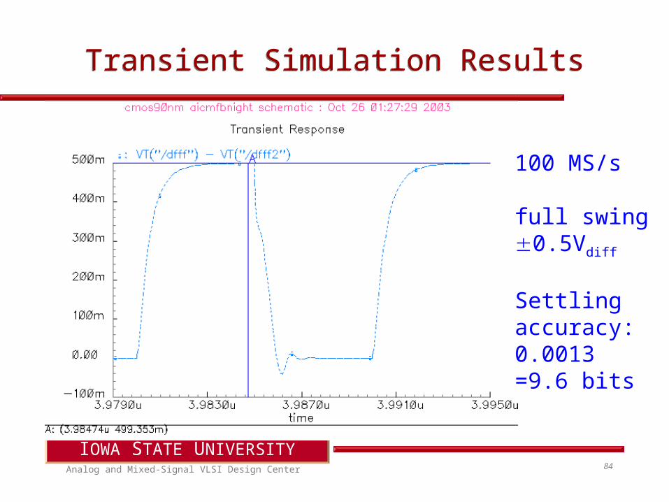
100 MS/s
full swing0.5Vdiff
Settlingaccuracy:0.0013=9.6 bits
Transient Simulation ResultsTransient Simulation Results
Analog and Mixed-Signal VLSI Design Center
IOWA STATE UNIVERSITY85
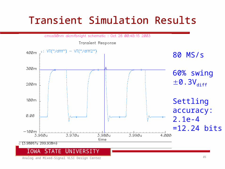
80 MS/s
60% swing0.3Vdiff
Settlingaccuracy:2.1e-4=12.24 bits
Transient Simulation ResultsTransient Simulation Results
Analog and Mixed-Signal VLSI Design Center
IOWA STATE UNIVERSITY86
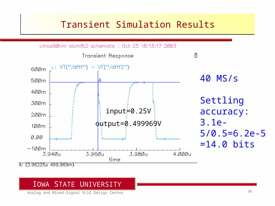
Transient Simulation ResultsTransient Simulation Results
input=0.25V
output=0.499969V
40 MS/s
Settling accuracy:3.1e-5/0.5=6.2e-5=14.0 bits
Analog and Mixed-Signal VLSI Design Center
IOWA STATE UNIVERSITY87
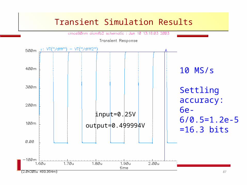
Transient Simulation ResultsTransient Simulation Results
input=0.25V
output=0.499994V
10 MS/s
Settling accuracy:6e-6/0.5=1.2e-5=16.3 bits

![OWA Operators in Decision Making - Semantic Scholar · OWA Operators in Decision Making ... Defi nition 1.3 A mapping S:[0,1] ... OWA weights as a column vector we shall fi nd it](https://img.pdfslide.us/doc/110x75/5d01f61c88c993c2488b950d/owa-operators-in-decision-making-semantic-scholar-owa-operators-in-decision.jpg)