Embed Size (px)
Citation preview
Composite Video Separatio
AN9644 Rev. 0.00Oct 1996
APPLICATION NOTE
n TechniquesAN9644
Rev. 0.00Oct 1996
IntroductionThe most fundamental job of a video decoder is to separatethe color from the black and white information for video com-posite signals. This task has been achieved many ways sincethe introduction of color television over 50 years ago. Manydifferent separation methods have been used through theyears. With the availability of new cost effective technolo-gies, the consumer has been seeing a gradual improvementin picture quality and detail. Advances in display tube technol-ogy and semiconductor processes have pushed the techno-logical envelope providing sharper, more robust video. Butseparating the chrominance from the luminance information isespecially challenging due to the fact that the signals overlapeach other in the frequency spectrum. How do you separatethem, while minimizing display artifacts?
Composite Signal Construction
The composite video signal is constructed with 3 basic elements:
- Luminance Information from DC to 5.5MHz (B&W Detail)
- Chrominance Information modulated onto a carrier (at3.58MHz or 4.43MHz)
- Synchronization Information (Horizontal and Vertical Sync)
The three analog elements of a composite video signal carryall the information necessary to display a two dimensionalpicture on a cathode ray tube (CRT) television.
Luminance (a B&W World)
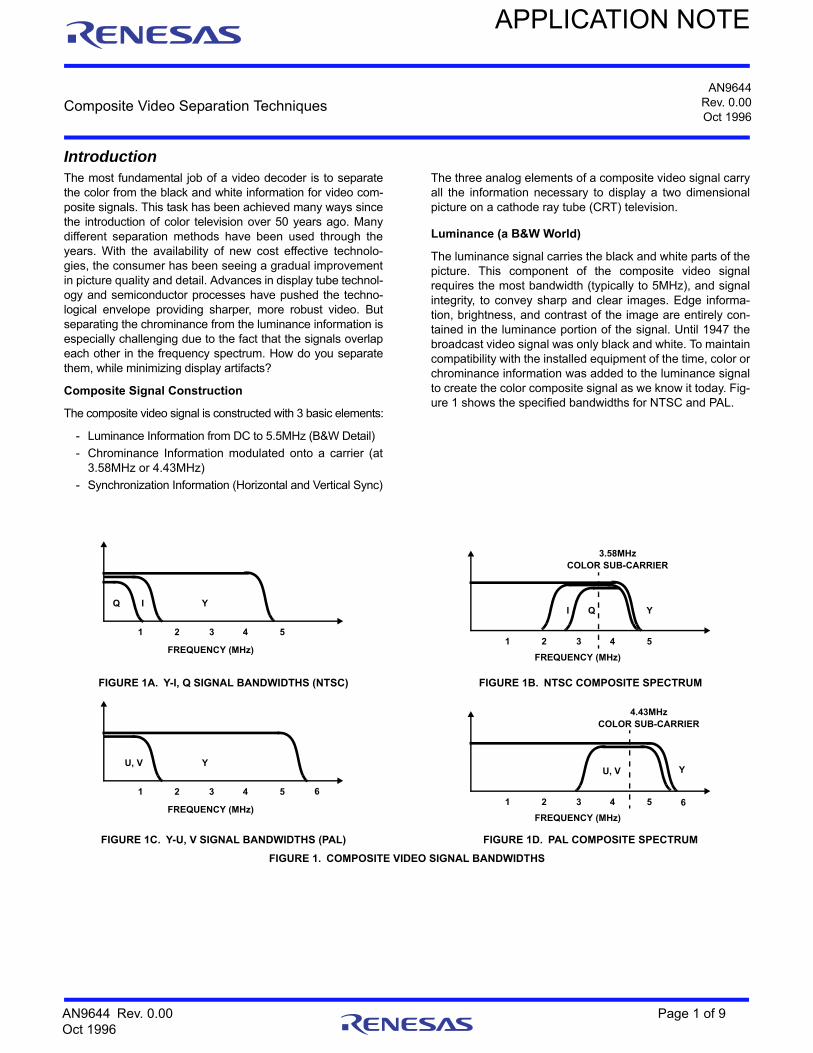
The luminance signal carries the black and white parts of thepicture. This component of the composite video signalrequires the most bandwidth (typically to 5MHz), and signalintegrity, to convey sharp and clear images. Edge informa-tion, brightness, and contrast of the image are entirely con-tained in the luminance portion of the signal. Until 1947 thebroadcast video signal was only black and white. To maintaincompatibility with the installed equipment of the time, color orchrominance information was added to the luminance signalto create the color composite signal as we know it today. Fig-ure 1 shows the specified bandwidths for NTSC and PAL.
FIGURE 1A. Y-I, Q SIGNAL BANDWIDTHS (NTSC) FIGURE 1B. NTSC COMPOSITE SPECTRUM
FIGURE 1C. Y-U, V SIGNAL BANDWIDTHS (PAL) FIGURE 1D. PAL COMPOSITE SPECTRUM
FIGURE 1. COMPOSITE VIDEO SIGNAL BANDWIDTHS
1 2 3 4 5
Q I Y
FREQUENCY (MHz)1 2 3 4 5
QI
FREQUENCY (MHz)
3.58MHzCOLOR SUB-CARRIER
Y
1 2 3 4 5
U, V Y
FREQUENCY (MHz)
61 2 3 4 5
U, V
FREQUENCY (MHz)
4.43MHzCOLOR SUB-CARRIER
Y
6
Page 1 of 9
Composite Video Separation
Techniques
Chrominance (an Add-On)
The chrominance information is quadrature modulated ontothe luminance information. The chrominance is interleaved intothe video signal bandwidth between luminance spectra. Thechrominance modulation scheme utilizes an I, Q (U, V for PAL)coordinate system where hue and saturation is in vector for-mat. A camera sensor captures light in Red, Green, and Blue(RGB) format. The RGB signal is converted into Y (luminancesignal) and I, Q (Color Difference signal) format along with thesynchronization information. The I, Q (commonly referred to asC) color information occupies a smaller bandwidth than the Ysignal. C bandwidths typically range from 0.6MHz to 1.3MHz.The chrominance signal is modulated onto a carrier. The car-rier resides at 3.58MHz for NTSC signals and 4.43MHz for PALsignals. The chroma information must be separated out of thevideo signal to demodulate it to baseband. This is difficultbecause luminance information that resides from 2MHz to5MHz cannot be differentiated from chroma information. Sev-eral techniques have been tried over the years to improve sep-arating Y and C, each increasing in complexity andperformance.
Don’t Forget the Sync
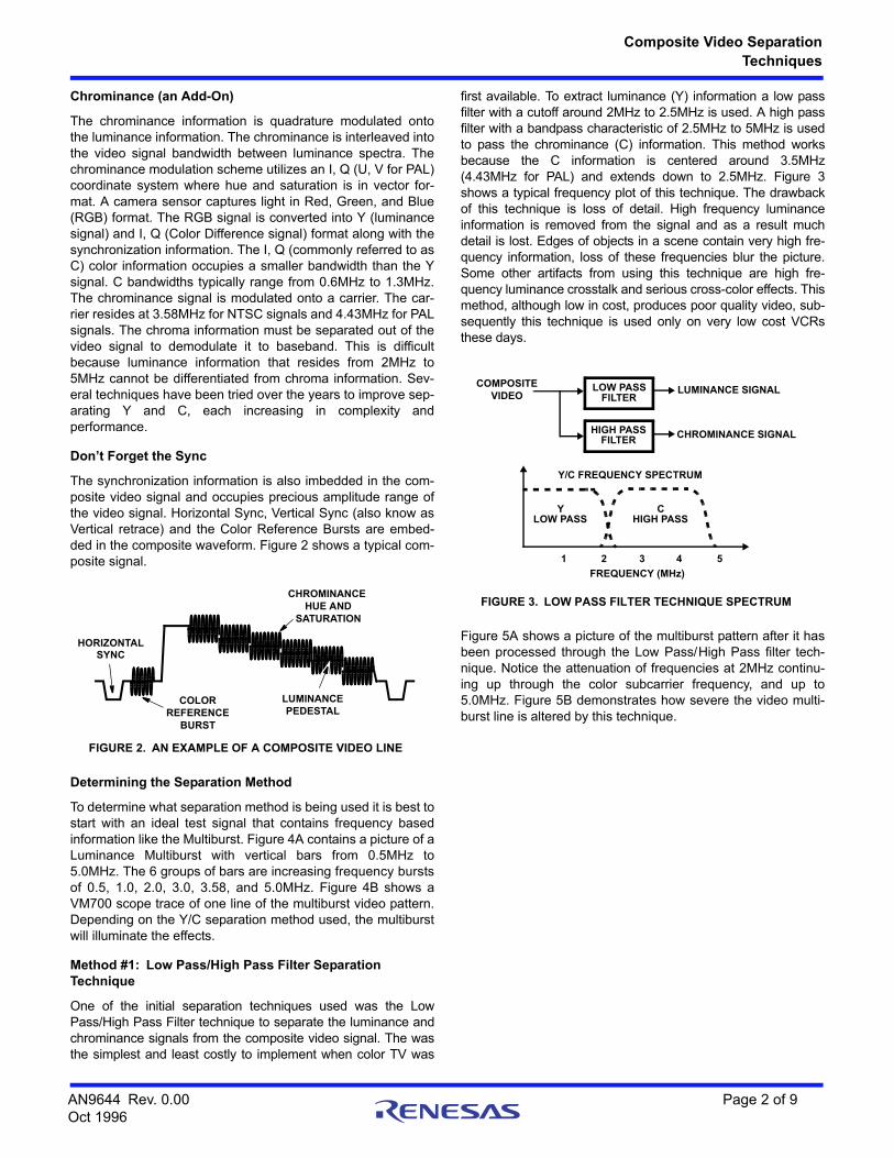
The synchronization information is also imbedded in the com-posite video signal and occupies precious amplitude range ofthe video signal. Horizontal Sync, Vertical Sync (also know asVertical retrace) and the Color Reference Bursts are embed-ded in the composite waveform. Figure 2 shows a typical com-posite signal.
Determining the Separation Method
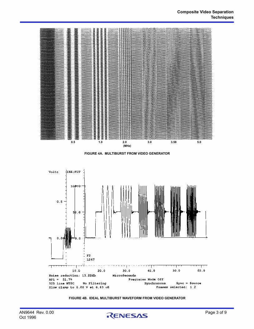
To determine what separation method is being used it is best tostart with an ideal test signal that contains frequency basedinformation like the Multiburst. Figure 4A contains a picture of aLuminance Multiburst with vertical bars from 0.5MHz to5.0MHz. The 6 groups of bars are increasing frequency burstsof 0.5, 1.0, 2.0, 3.0, 3.58, and 5.0MHz. Figure 4B shows aVM700 scope trace of one line of the multiburst video pattern.Depending on the Y/C separation method used, the multiburstwill illuminate the effects.
Method #1: Low Pass/High Pass Filter SeparationTechnique
One of the initial separation techniques used was the LowPass/High Pass Filter technique to separate the luminance andchrominance signals from the composite video signal. The wasthe simplest and least costly to implement when color TV was
first available. To extract luminance (Y) information a low passfilter with a cutoff around 2MHz to 2.5MHz is used. A high passfilter with a bandpass characteristic of 2.5MHz to 5MHz is usedto pass the chrominance (C) information. This method worksbecause the C information is centered around 3.5MHz(4.43MHz for PAL) and extends down to 2.5MHz. Figure 3shows a typical frequency plot of this technique. The drawbackof this technique is loss of detail. High frequency luminanceinformation is removed from the signal and as a result muchdetail is lost. Edges of objects in a scene contain very high fre-quency information, loss of these frequencies blur the picture.Some other artifacts from using this technique are high fre-quency luminance crosstalk and serious cross-color effects. Thismethod, although low in cost, produces poor quality video, sub-sequently this technique is used only on very low cost VCRsthese days.
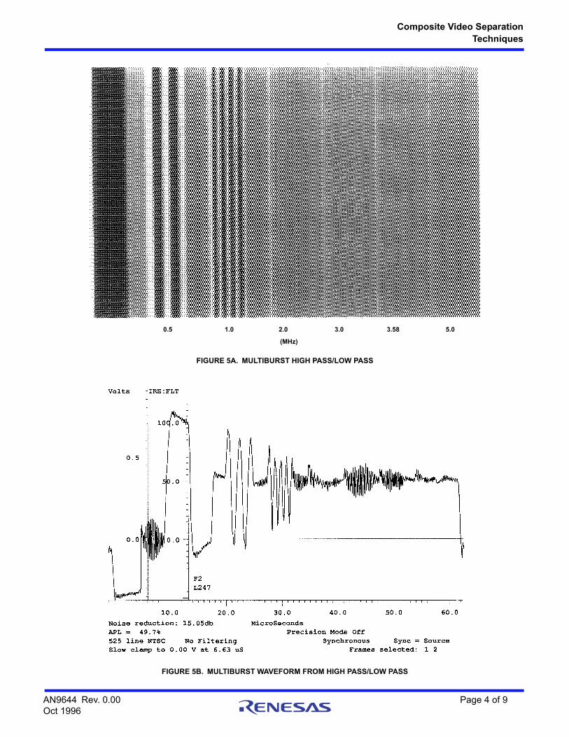
Figure 5A shows a picture of the multiburst pattern after it hasbeen processed through the Low Pass/High Pass filter tech-nique. Notice the attenuation of frequencies at 2MHz continu-ing up through the color subcarrier frequency, and up to5.0MHz. Figure 5B demonstrates how severe the video multi-burst line is altered by this technique.
HORIZONTALSYNC
COLORREFERENCE
BURST
PEDESTAL
CHROMINANCE HUE AND
SATURATION
FIGURE 2. AN EXAMPLE OF A COMPOSITE VIDEO LINE
LUMINANCE
1 2 3 4 5
Y/C FREQUENCY SPECTRUM
FREQUENCY (MHz)
YLOW PASS
CHIGH PASS
COMPOSITEVIDEO
LUMINANCE SIGNAL
CHROMINANCE SIGNAL
FIGURE 3. LOW PASS FILTER TECHNIQUE SPECTRUM
LOW PASSFILTER
HIGH PASSFILTER
AN9644 Rev. 0.00 Page 2 of 9Oct 1996
Composite Video Separation
Techniques
FIGURE 4A. MULTIBURST FROM VIDEO GENERATOR
FIGURE 4B. IDEAL MULTIBURST WAVEFORM FROM VIDEO GENERATOR
0.5 1.0 2.0 3.0 3.58 5.0(MHz)
AN9644 Rev. 0.00 Page 3 of 9Oct 1996
Composite Video Separation
Techniques
FIGURE 5A. MULTIBURST HIGH PASS/LOW PASS
FIGURE 5B. MULTIBURST WAVEFORM FROM HIGH PASS/LOW PASS
0.5 1.0 2.0 3.0 3.58 5.0
(MHz)
AN9644 Rev. 0.00 Page 4 of 9Oct 1996
Composite Video Separation
Techniques
Method #2: Color Trap Filter Separation Technique
Another technique to separate Y and C is the color trap filtermethod. A notch filter centered at the color subcarrier frequency isused to extract C information from 2.5MHz to 4.5MHz. Figure 6shows the frequency plot of this technique. This method has twodrawbacks to it. First, it limits the C bandwidth (which extends to2.1MHz) cutting out fine color detail. Second, luminance informa-tion in the notch frequency range contaminates the C signal andgenerates unwanted color or rainbows. This is most noticeablewith pictures that contain closely spaced black and white lines, likewhen a person wearing a herringbone jacket is recorded. Thehigh frequency luminance will produce rainbows of colors due tothe cross color effects.
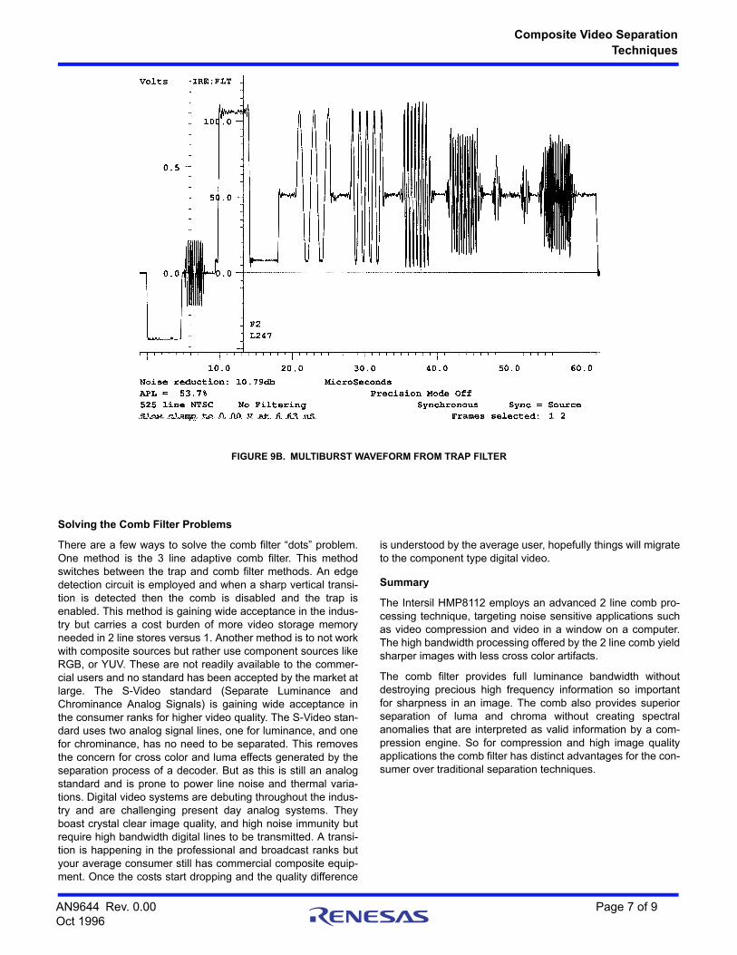
Figure 9A shows a picture of the multiburst pattern after it hasbeen processed through the Trap filter technique. Notice theattenuation of frequencies at 3.58MHz color subcarrier fre-quency continuing up through the color subcarrier frequency,and up to 5.0MHz. Figure 9B demonstrates how severe thevideo multiburst line is altered by this technique.
Comb Filter Separation Technique
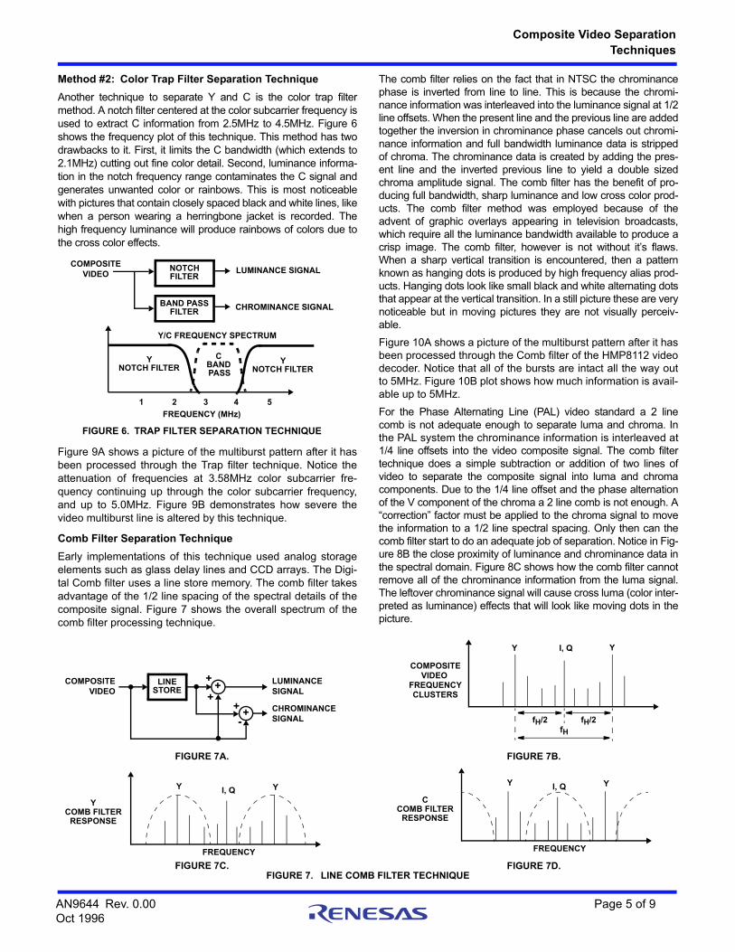
Early implementations of this technique used analog storageelements such as glass delay lines and CCD arrays. The Digi-tal Comb filter uses a line store memory. The comb filter takesadvantage of the 1/2 line spacing of the spectral details of thecomposite signal. Figure 7 shows the overall spectrum of thecomb filter processing technique.
The comb filter relies on the fact that in NTSC the chrominancephase is inverted from line to line. This is because the chromi-nance information was interleaved into the luminance signal at 1/2line offsets. When the present line and the previous line are addedtogether the inversion in chrominance phase cancels out chromi-nance information and full bandwidth luminance data is strippedof chroma. The chrominance data is created by adding the pres-ent line and the inverted previous line to yield a double sizedchroma amplitude signal. The comb filter has the benefit of pro-ducing full bandwidth, sharp luminance and low cross color prod-ucts. The comb filter method was employed because of theadvent of graphic overlays appearing in television broadcasts,which require all the luminance bandwidth available to produce acrisp image. The comb filter, however is not without it’s flaws.When a sharp vertical transition is encountered, then a patternknown as hanging dots is produced by high frequency alias prod-ucts. Hanging dots look like small black and white alternating dotsthat appear at the vertical transition. In a still picture these are verynoticeable but in moving pictures they are not visually perceiv-able.
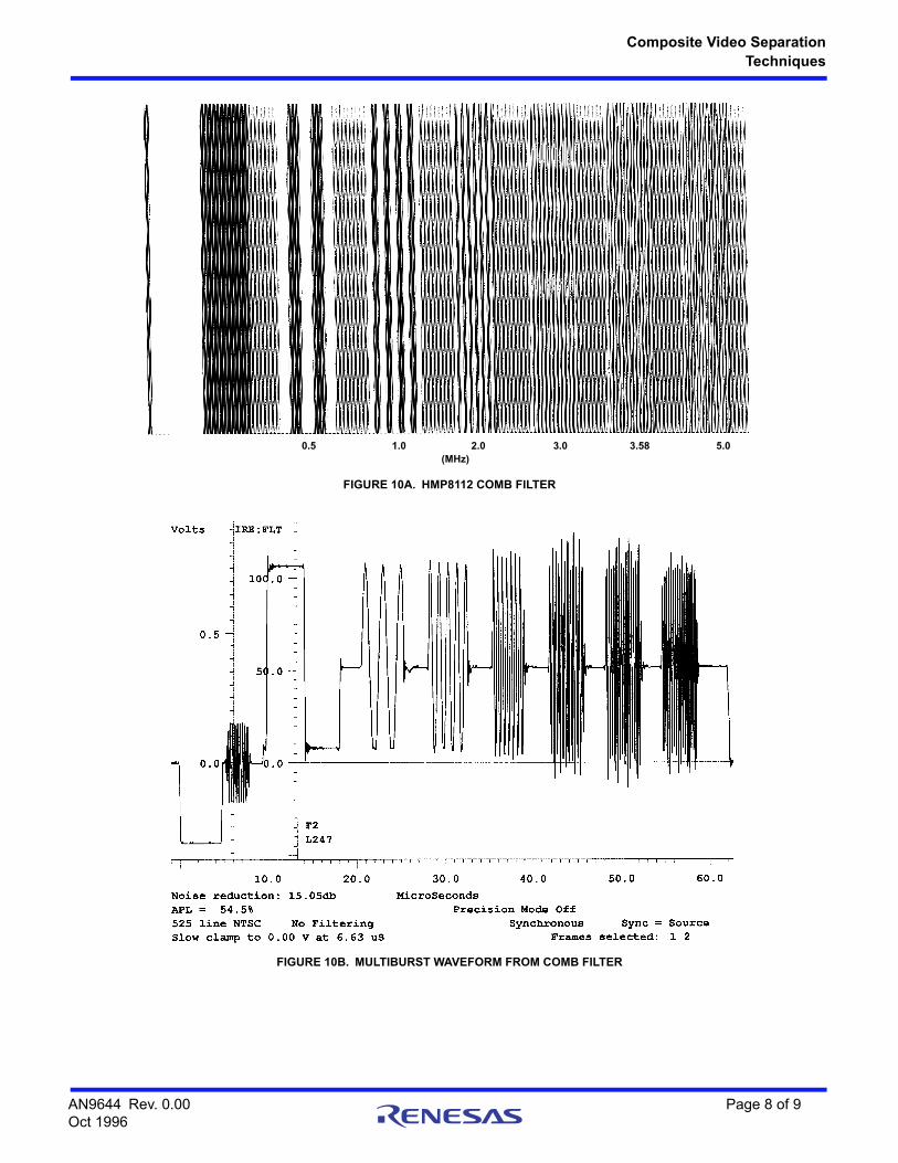
Figure 10A shows a picture of the multiburst pattern after it hasbeen processed through the Comb filter of the HMP8112 videodecoder. Notice that all of the bursts are intact all the way outto 5MHz. Figure 10B plot shows how much information is avail-able up to 5MHz.
For the Phase Alternating Line (PAL) video standard a 2 linecomb is not adequate enough to separate luma and chroma. Inthe PAL system the chrominance information is interleaved at1/4 line offsets into the video composite signal. The comb filtertechnique does a simple subtraction or addition of two lines ofvideo to separate the composite signal into luma and chromacomponents. Due to the 1/4 line offset and the phase alternationof the V component of the chroma a 2 line comb is not enough. A“correction” factor must be applied to the chroma signal to movethe information to a 1/2 line spectral spacing. Only then can thecomb filter start to do an adequate job of separation. Notice in Fig-ure 8B the close proximity of luminance and chrominance data inthe spectral domain. Figure 8C shows how the comb filter cannotremove all of the chrominance information from the luma signal.The leftover chrominance signal will cause cross luma (color inter-preted as luminance) effects that will look like moving dots in thepicture.
1 2 3 4 5
Y/C FREQUENCY SPECTRUM
FREQUENCY (MHz)
YNOTCH FILTER
CBAND
COMPOSITEVIDEO LUMINANCE SIGNAL
CHROMINANCE SIGNAL
NOTCHFILTER
BAND PASSFILTER
PASS
YNOTCH FILTER
FIGURE 6. TRAP FILTER SEPARATION TECHNIQUE
FIGURE 7A. FIGURE 7B.
FIGURE 7C. FIGURE 7D.FIGURE 7. LINE COMB FILTER TECHNIQUE
COMPOSITEVIDEO
LUMINANCE
CHROMINANCE
SIGNAL
SIGNAL
+
-
++
LINESTORE +
+fH/2 fH/2
fH
Y I, Q Y
COMPOSITEVIDEO
FREQUENCYCLUSTERS
FREQUENCY
Y YI, Q
YCOMB FILTER
RESPONSE
FREQUENCY
Y YI, Q
CCOMB FILTER
RESPONSE
AN9644 Rev. 0.00 Page 5 of 9Oct 1996
Composite Video Separation
Techniques
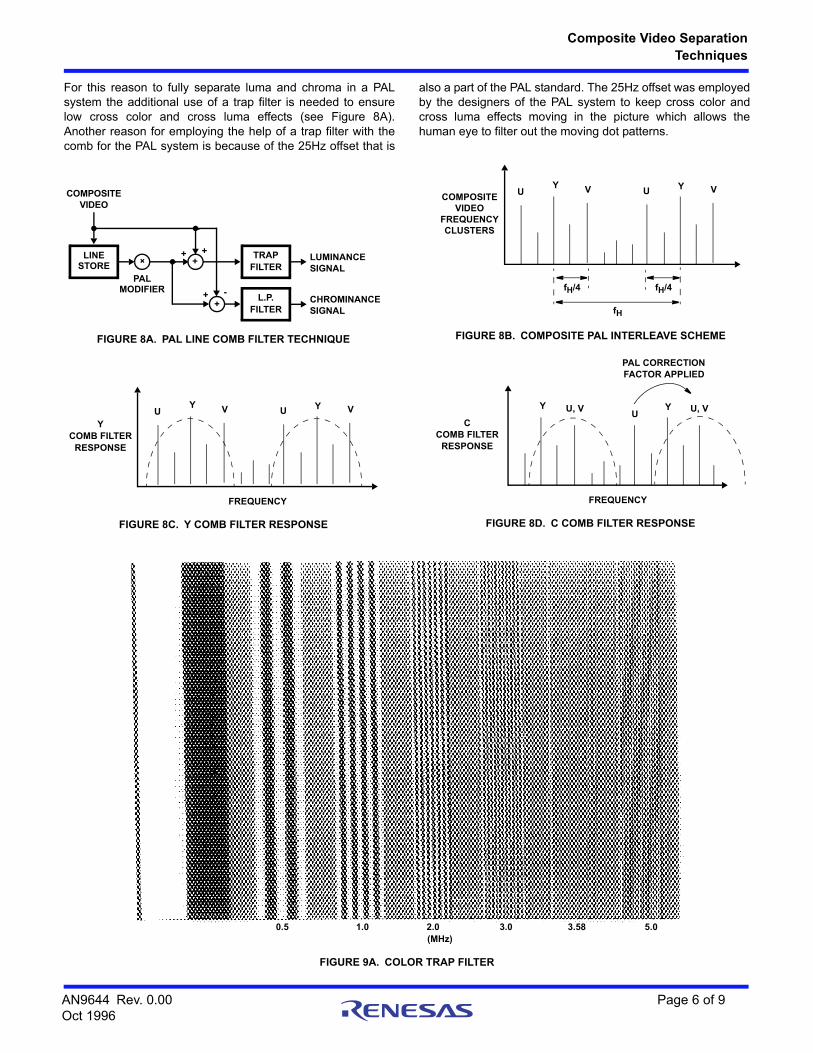
For this reason to fully separate luma and chroma in a PALsystem the additional use of a trap filter is needed to ensurelow cross color and cross luma effects (see Figure 8A).Another reason for employing the help of a trap filter with thecomb for the PAL system is because of the 25Hz offset that is
also a part of the PAL standard. The 25Hz offset was employedby the designers of the PAL system to keep cross color andcross luma effects moving in the picture which allows thehuman eye to filter out the moving dot patterns.
FIGURE 8A. PAL LINE COMB FILTER TECHNIQUE FIGURE 8B. COMPOSITE PAL INTERLEAVE SCHEME
FIGURE 8C. Y COMB FILTER RESPONSE FIGURE 8D. C COMB FILTER RESPONSE
FIGURE 9A. COLOR TRAP FILTER
COMPOSITEVIDEO
LUMINANCE
CHROMINANCE
SIGNAL
SIGNAL
+
-+
+LINESTORE +
+
+
PALMODIFIER
TRAPFILTER
L.P.FILTER
COMPOSITE
fH/4
fH
Y Y
fH/4
U
VIDEOFREQUENCYCLUSTERS
VU V
FREQUENCY
YCOMB FILTER
RESPONSE
Y YU VU V
FREQUENCY
C
Y YU, VU
COMB FILTERRESPONSE
U, V
PAL CORRECTIONFACTOR APPLIED
0.5 1.0 2.0 3.0 3.58 5.0(MHz)
AN9644 Rev. 0.00 Page 6 of 9Oct 1996
Composite Video Separation
Techniques
Solving the Comb Filter Problems
There are a few ways to solve the comb filter “dots” problem.One method is the 3 line adaptive comb filter. This methodswitches between the trap and comb filter methods. An edgedetection circuit is employed and when a sharp vertical transi-tion is detected then the comb is disabled and the trap isenabled. This method is gaining wide acceptance in the indus-try but carries a cost burden of more video storage memoryneeded in 2 line stores versus 1. Another method is to not workwith composite sources but rather use component sources likeRGB, or YUV. These are not readily available to the commer-cial users and no standard has been accepted by the market atlarge. The S-Video standard (Separate Luminance andChrominance Analog Signals) is gaining wide acceptance inthe consumer ranks for higher video quality. The S-Video stan-dard uses two analog signal lines, one for luminance, and onefor chrominance, has no need to be separated. This removesthe concern for cross color and luma effects generated by theseparation process of a decoder. But as this is still an analogstandard and is prone to power line noise and thermal varia-tions. Digital video systems are debuting throughout the indus-try and are challenging present day analog systems. Theyboast crystal clear image quality, and high noise immunity butrequire high bandwidth digital lines to be transmitted. A transi-tion is happening in the professional and broadcast ranks butyour average consumer still has commercial composite equip-ment. Once the costs start dropping and the quality difference
is understood by the average user, hopefully things will migrateto the component type digital video.
Summary
The Intersil HMP8112 employs an advanced 2 line comb pro-cessing technique, targeting noise sensitive applications suchas video compression and video in a window on a computer.The high bandwidth processing offered by the 2 line comb yieldsharper images with less cross color artifacts.
The comb filter provides full luminance bandwidth withoutdestroying precious high frequency information so importantfor sharpness in an image. The comb also provides superiorseparation of luma and chroma without creating spectralanomalies that are interpreted as valid information by a com-pression engine. So for compression and high image qualityapplications the comb filter has distinct advantages for the con-sumer over traditional separation techniques.
FIGURE 9B. MULTIBURST WAVEFORM FROM TRAP FILTER
AN9644 Rev. 0.00 Page 7 of 9Oct 1996
Composite Video Separation
Techniques
FIGURE 10A. HMP8112 COMB FILTER
FIGURE 10B. MULTIBURST WAVEFORM FROM COMB FILTER
0.5 1.0 2.0 3.0 3.58 5.0(MHz)
AN9644 Rev. 0.00 Page 8 of 9Oct 1996
http://www.renesas.comRefer to "http://www.renesas.com/" for the latest and detailed information.
Renesas Electronics America Inc.1001 Murphy Ranch Road, Milpitas, CA 95035, U.S.A.Tel: +1-408-432-8888, Fax: +1-408-434-5351Renesas Electronics Canada Limited9251 Yonge Street, Suite 8309 Richmond Hill, Ontario Canada L4C 9T3Tel: +1-905-237-2004Renesas Electronics Europe LimitedDukes Meadow, Millboard Road, Bourne End, Buckinghamshire, SL8 5FH, U.KTel: +44-1628-651-700, Fax: +44-1628-651-804Renesas Electronics Europe GmbHArcadiastrasse 10, 40472 Düsseldorf, Germany Tel: +49-211-6503-0, Fax: +49-211-6503-1327Renesas Electronics (China) Co., Ltd.Room 1709 Quantum Plaza, No.27 ZhichunLu, Haidian District, Beijing, 100191 P. R. ChinaTel: +86-10-8235-1155, Fax: +86-10-8235-7679Renesas Electronics (Shanghai) Co., Ltd.Unit 301, Tower A, Central Towers, 555 Langao Road, Putuo District, Shanghai, 200333 P. R. China Tel: +86-21-2226-0888, Fax: +86-21-2226-0999Renesas Electronics Hong Kong LimitedUnit 1601-1611, 16/F., Tower 2, Grand Century Place, 193 Prince Edward Road West, Mongkok, Kowloon, Hong KongTel: +852-2265-6688, Fax: +852 2886-9022Renesas Electronics Taiwan Co., Ltd.13F, No. 363, Fu Shing North Road, Taipei 10543, TaiwanTel: +886-2-8175-9600, Fax: +886 2-8175-9670Renesas Electronics Singapore Pte. Ltd.80 Bendemeer Road, Unit #06-02 Hyflux Innovation Centre, Singapore 339949Tel: +65-6213-0200, Fax: +65-6213-0300Renesas Electronics Malaysia Sdn.Bhd.Unit 1207, Block B, Menara Amcorp, Amcorp Trade Centre, No. 18, Jln Persiaran Barat, 46050 Petaling Jaya, Selangor Darul Ehsan, MalaysiaTel: +60-3-7955-9390, Fax: +60-3-7955-9510Renesas Electronics India Pvt. Ltd.No.777C, 100 Feet Road, HAL 2nd Stage, Indiranagar, Bangalore 560 038, IndiaTel: +91-80-67208700, Fax: +91-80-67208777Renesas Electronics Korea Co., Ltd.17F, KAMCO Yangjae Tower, 262, Gangnam-daero, Gangnam-gu, Seoul, 06265 KoreaTel: +82-2-558-3737, Fax: +82-2-558-5338
SALES OFFICES
© 2018 Renesas Electronics Corporation. All rights reserved.Colophon 7.0
(Rev.4.0-1 November 2017)
Notice
1. Descriptions of circuits, software and other related information in this document are provided only to illustrate the operation of semiconductor products and application examples. You are fully responsible for
the incorporation or any other use of the circuits, software, and information in the design of your product or system. Renesas Electronics disclaims any and all liability for any losses and damages incurred by
you or third parties arising from the use of these circuits, software, or information.
2. Renesas Electronics hereby expressly disclaims any warranties against and liability for infringement or any other claims involving patents, copyrights, or other intellectual property rights of third parties, by or
arising from the use of Renesas Electronics products or technical information described in this document, including but not limited to, the product data, drawings, charts, programs, algorithms, and application
examples.
3. No license, express, implied or otherwise, is granted hereby under any patents, copyrights or other intellectual property rights of Renesas Electronics or others.
4. You shall not alter, modify, copy, or reverse engineer any Renesas Electronics product, whether in whole or in part. Renesas Electronics disclaims any and all liability for any losses or damages incurred by
you or third parties arising from such alteration, modification, copying or reverse engineering.
5. Renesas Electronics products are classified according to the following two quality grades: “Standard” and “High Quality”. The intended applications for each Renesas Electronics product depends on the
product’s quality grade, as indicated below.
"Standard": Computers; office equipment; communications equipment; test and measurement equipment; audio and visual equipment; home electronic appliances; machine tools; personal electronic
equipment; industrial robots; etc.
"High Quality": Transportation equipment (automobiles, trains, ships, etc.); traffic control (traffic lights); large-scale communication equipment; key financial terminal systems; safety control equipment; etc.
Unless expressly designated as a high reliability product or a product for harsh environments in a Renesas Electronics data sheet or other Renesas Electronics document, Renesas Electronics products are
not intended or authorized for use in products or systems that may pose a direct threat to human life or bodily injury (artificial life support devices or systems; surgical implantations; etc.), or may cause
serious property damage (space system; undersea repeaters; nuclear power control systems; aircraft control systems; key plant systems; military equipment; etc.). Renesas Electronics disclaims any and all
liability for any damages or losses incurred by you or any third parties arising from the use of any Renesas Electronics product that is inconsistent with any Renesas Electronics data sheet, user’s manual or
other Renesas Electronics document.
6. When using Renesas Electronics products, refer to the latest product information (data sheets, user’s manuals, application notes, “General Notes for Handling and Using Semiconductor Devices” in the
reliability handbook, etc.), and ensure that usage conditions are within the ranges specified by Renesas Electronics with respect to maximum ratings, operating power supply voltage range, heat dissipation
characteristics, installation, etc. Renesas Electronics disclaims any and all liability for any malfunctions, failure or accident arising out of the use of Renesas Electronics products outside of such specified
ranges.
7. Although Renesas Electronics endeavors to improve the quality and reliability of Renesas Electronics products, semiconductor products have specific characteristics, such as the occurrence of failure at a
certain rate and malfunctions under certain use conditions. Unless designated as a high reliability product or a product for harsh environments in a Renesas Electronics data sheet or other Renesas
Electronics document, Renesas Electronics products are not subject to radiation resistance design. You are responsible for implementing safety measures to guard against the possibility of bodily injury, injury
or damage caused by fire, and/or danger to the public in the event of a failure or malfunction of Renesas Electronics products, such as safety design for hardware and software, including but not limited to
redundancy, fire control and malfunction prevention, appropriate treatment for aging degradation or any other appropriate measures. Because the evaluation of microcomputer software alone is very difficult
and impractical, you are responsible for evaluating the safety of the final products or systems manufactured by you.
8. Please contact a Renesas Electronics sales office for details as to environmental matters such as the environmental compatibility of each Renesas Electronics product. You are responsible for carefully and
sufficiently investigating applicable laws and regulations that regulate the inclusion or use of controlled substances, including without limitation, the EU RoHS Directive, and using Renesas Electronics
products in compliance with all these applicable laws and regulations. Renesas Electronics disclaims any and all liability for damages or losses occurring as a result of your noncompliance with applicable
laws and regulations.
9. Renesas Electronics products and technologies shall not be used for or incorporated into any products or systems whose manufacture, use, or sale is prohibited under any applicable domestic or foreign laws
or regulations. You shall comply with any applicable export control laws and regulations promulgated and administered by the governments of any countries asserting jurisdiction over the parties or
transactions.
10. It is the responsibility of the buyer or distributor of Renesas Electronics products, or any other party who distributes, disposes of, or otherwise sells or transfers the product to a third party, to notify such third
party in advance of the contents and conditions set forth in this document.
11. This document shall not be reprinted, reproduced or duplicated in any form, in whole or in part, without prior written consent of Renesas Electronics.
12. Please contact a Renesas Electronics sales office if you have any questions regarding the information contained in this document or Renesas Electronics products.
(Note 1) “Renesas Electronics” as used in this document means Renesas Electronics Corporation and also includes its directly or indirectly controlled subsidiaries.
(Note 2) “Renesas Electronics product(s)” means any product developed or manufactured by or for Renesas Electronics.