Embed Size (px)
Citation preview
AN926: Reading and Writing Registerswith SPI and I2C
The Si534x/8x timing devices use either SPI or I2C as the communication protocol forchanging internal register settings in the chip. This application note clarifies how to ac-cess the Si534x/8x registers with examples using these two protocols.
While a microcontroller is often used to read/write registers on the device, an SPI orI2C bus analyzer can also be used. Companies, such as Corelis (www.corelis.com) orTotal Phase/Ardvark (http://www.totalphase.com), sell both I2C and SPI bus analyzersthat connect through USB to the PC and have GUI interfaces. The user simply con-nects the wires (GND, CS, MISO, MOSI, and SCLK pins for SPI or SDA, SCLK, andGND pins for I2C) of the hardware (slave). The bus analyzer handles the low-level con-trol of the bus. The commands and data are sent through a GUI on the PC. This is of-ten a quick way to evaluate a chip requiring one of these serial interfaces when thedriver code is not easily available. It is always important to make sure the hardware isconnected and configured correctly for proper operation.
The examples provided in this application note can be followed regardless of the hard-ware chosen to connect to the Si534x/8x device.
KEY POINTS
• SPI and I2C communication available• SPI command protocol provided• Step-by-step code examples provided for
SPI and I2C
APPLIED DEVICES
• Si534x• Si538x• Si539x
silabs.com | Building a more connected world. Rev. 0.2
1. Introduction
In the Si538x/4x, a register is 1 byte (8-bits) wide, and an address is 2 bytes (16-bits) wide. Due to single byte addressing used on theI2C and SPI interfaces, a special PAGE register is used to specify the 2 byte address. The first byte in the 2 byte address is always thePAGE, and the PAGE is always located at register 0x01. It is copied on every address page. Therefore, address 0001= Page; 0101=Page; 0201=Page, etc. A named setting, such as “MXAXB_NUM”, is a contiguous range of bits within one or more registers. A namedsetting will never span a page boundary. For example:
Named Setting Location
DEVICE_GRADE 0x0004[7:0] A full byte at page 0x00, serial interface ad-dress 0x04
MXAXB_NUM 0x0235[0:43]
0x0235[7:0]
0x0236[7:0]
0x0237[7:0]
0x0238[7:0]
0x0239[7:0]
0x023A[3:0]
5 full bytes, 1 partial byte located at page0x02 interface address 0x35 through 0x3A
The Register Map section of the device Family Reference Manual has more information on registers and addressing.
AN926: Reading and Writing Registers with SPI and I2CIntroduction
silabs.com | Building a more connected world. Rev. 0.2 | 2
2. SPI Protocol
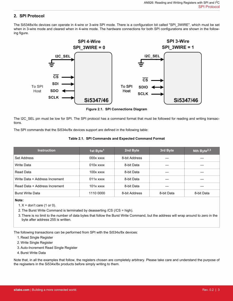
The Si5348x/4x devices can operate in 4-wire or 3-wire SPI mode. There is a configuration bit called "SPI_3WIRE", which must be setwhen in 3-wire mode and cleared when in 4-wire mode. The hardware connections for both SPI configurations are shown in the follow-ing figure.
Figure 2.1. SPI Connections Diagram
The I2C_SEL pin must be low for SPI. The SPI protocol has a command format that must be followed for reading and writing transac-tions.
The SPI commands that the Si534x/8x devices support are defined in the following table:
Table 2.1. SPI Commands and Expected Command Format
Instruction 1st Byte1 2nd Byte 3rd Byte Nth Byte2,3
Set Address 000x xxxx 8-bit Address — —
Write Data 010x xxxx 8-bit Data — —
Read Data 100x xxxx 8-bit Data — —
Write Data + Address Increment 011x xxxx 8-bit Data — —
Read Data + Address Increment 101x xxxx 8-bit Data — —
Burst Write Data 1110 0000 8-bit Address 8-bit Data 8-bit Data
Note:1. X = don’t care (1 or 0).2. The Burst Write Command is terminated by deasserting /CS (/CS = high).3. There is no limit to the number of data bytes that follow the Burst Write Command, but the address will wrap around to zero in the
byte after address 255 is written.
The following transactions can be performed from SPI with the Si534x/8x devices:1. Read Single Register2. Write Single Register3. Auto-Increment Read Single Register4. Burst Write Data
Note that, in all the examples that follow, the registers chosen are completely arbitrary. Please take care and understand the purpose ofthe regiseters in the Si534x/8x products before simply writing to them.
AN926: Reading and Writing Registers with SPI and I2CSPI Protocol
silabs.com | Building a more connected world. Rev. 0.2 | 3
The following examples use the "SPI_Run" function, which is written for an 8051 Silicon Labs MCU, as follows:
U8 SPI_Run(U8 command, U8 val) { P0_3 = 0; // Set Chip Select line low SPI0CN |= 0x01 // Enable the SPI Port SPI0DAT = command // send the command byte to the DUT while (SPIF == 0 ) {} // Wait for transfer to complete SPIF = 0; // Clear the SPI interrupt flag spi _read_data = SPI0DAT; // Clear the SPI receive buffer
SPI0DAT = val; // Send the value or data to the DUT while (SPIF == 0 ) {} // Wait for transfer to complete SPIF = 0; // Clear the SPI interrupt flag P0_3 = 1; // Set Chip Select line high spi_read_data=SPI0DAT; return spi_read_data; // return the data from the receive buffer }
2.1 Example 1: Read from Register 0x052A
1. Run the SPI bus to send out 0x00 for the “Set Address” command followed by the PAGE register location (0x01). This sets theaddress to point to 0x01, which is the register for changing the page value:
SPI_Run (0x00, 0x01) // Set Address to Register 0x01 (PAGE register)
2. Run the SPI bus to write the page value of 0x05, since the address is pointing at the PAGE register. First send out the “write”command 0x40, followed by the value 0x05:
SPI_Run (0x40, 0x05) // Write Value 0x05
3. Run the SPI bus to point to the register 0x2A. This is done by using the “Set Address” command followed by the register 0x2A:
SPI_Run (0x00, 0x2A) //Set Address to Register 0x2A
4. Send the Read Command followed by a dummy write. The dummy write is needed because the SPI bus sends data out to receivedata in:
Data = SPI_Run (0x80, 0xFF) //Send the read command and receive data from register 0x052A
At this point, the SPI bus value from register 0x052A is returned into “Data”:
//Full Example 1
PAGE = 0x01; Byte SPI_Reg_Read(u16 Reg) { Byte page_byte; Byte reg_byte; page_byte = Reg>>8; reg_byte=Reg; SPI_Run(0x00, PAGE); SPI_Run(0x40, page_byte); SPI_Run(0x00, reg_byte); Return SPI_Run (0x80, 0xFF); }
AN926: Reading and Writing Registers with SPI and I2CSPI Protocol
silabs.com | Building a more connected world. Rev. 0.2 | 4
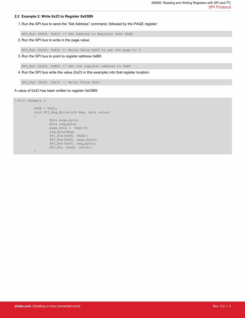
2.2 Example 2: Write 0x23 to Register 0x03B9
1. Run the SPI bus to send the “Set Address” command, followed by the PAGE register:
SPI_Run (0x00, 0x01) // Set Address to Register 0x01 PAGE
2. Run the SPI bus to write in the page value:
SPI_Run (0x40, 0x03) // Write Value 0x03 to set the page to 3
3. Run the SPI bus to point to register address 0xB9:
SPI_Run (0x00, 0xB9) // Set the register address to 0xB9
4. Run the SPI bus write the value (0x23 in this example) into that register location:
SPI_Run (0x40, 0x23) // Write Value 0x23
A value of 0x23 has been written to register 0x03B9:
//Full Example 2
PAGE = 0x01; void SPI_Reg_Write(u16 Reg, byte value) { Byte page_byte; Byte reg_byte; page_byte = Reg>>8; reg_byte=Reg; SPI_Run(0x00, PAGE); SPI_Run(0x40, page_byte); SPI_Run(0x00, reg_byte); SPI_Run (0x40, value); }
AN926: Reading and Writing Registers with SPI and I2CSPI Protocol
silabs.com | Building a more connected world. Rev. 0.2 | 5
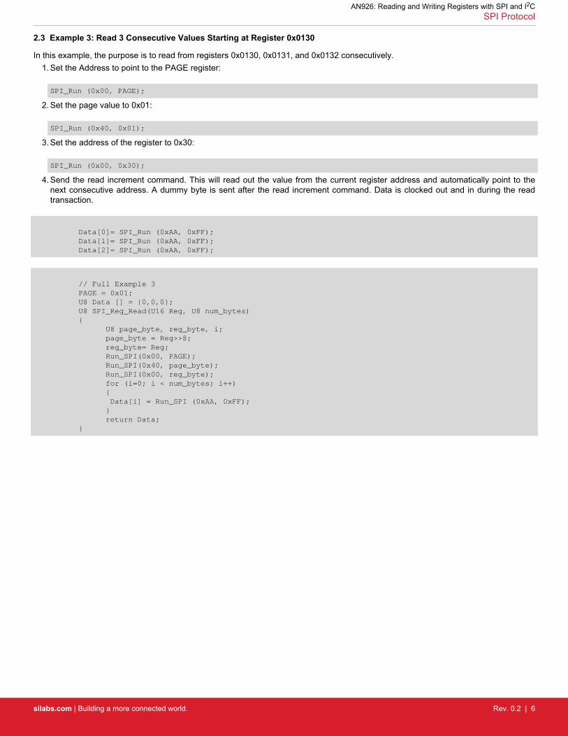
2.3 Example 3: Read 3 Consecutive Values Starting at Register 0x0130
In this example, the purpose is to read from registers 0x0130, 0x0131, and 0x0132 consecutively.1. Set the Address to point to the PAGE register:
SPI_Run (0x00, PAGE);
2. Set the page value to 0x01:
SPI_Run (0x40, 0x01);
3. Set the address of the register to 0x30:
SPI_Run (0x00, 0x30);
4. Send the read increment command. This will read out the value from the current register address and automatically point to thenext consecutive address. A dummy byte is sent after the read increment command. Data is clocked out and in during the readtransaction.
Data[0]= SPI_Run (0xAA, 0xFF); Data[1]= SPI_Run (0xAA, 0xFF); Data[2]= SPI_Run (0xAA, 0xFF);
// Full Example 3 PAGE = 0x01; U8 Data [] = {0,0,0}; U8 SPI_Reg_Read(U16 Reg, U8 num_bytes) { U8 page_byte, reg_byte, i; page_byte = Reg>>8; reg_byte= Reg; Run_SPI(0x00, PAGE); Run_SPI(0x40, page_byte); Run_SPI(0x00, reg_byte); for (i=0; i < num_bytes; i++) { Data[i] = Run_SPI (0xAA, 0xFF); } return Data; }
AN926: Reading and Writing Registers with SPI and I2CSPI Protocol
silabs.com | Building a more connected world. Rev. 0.2 | 6
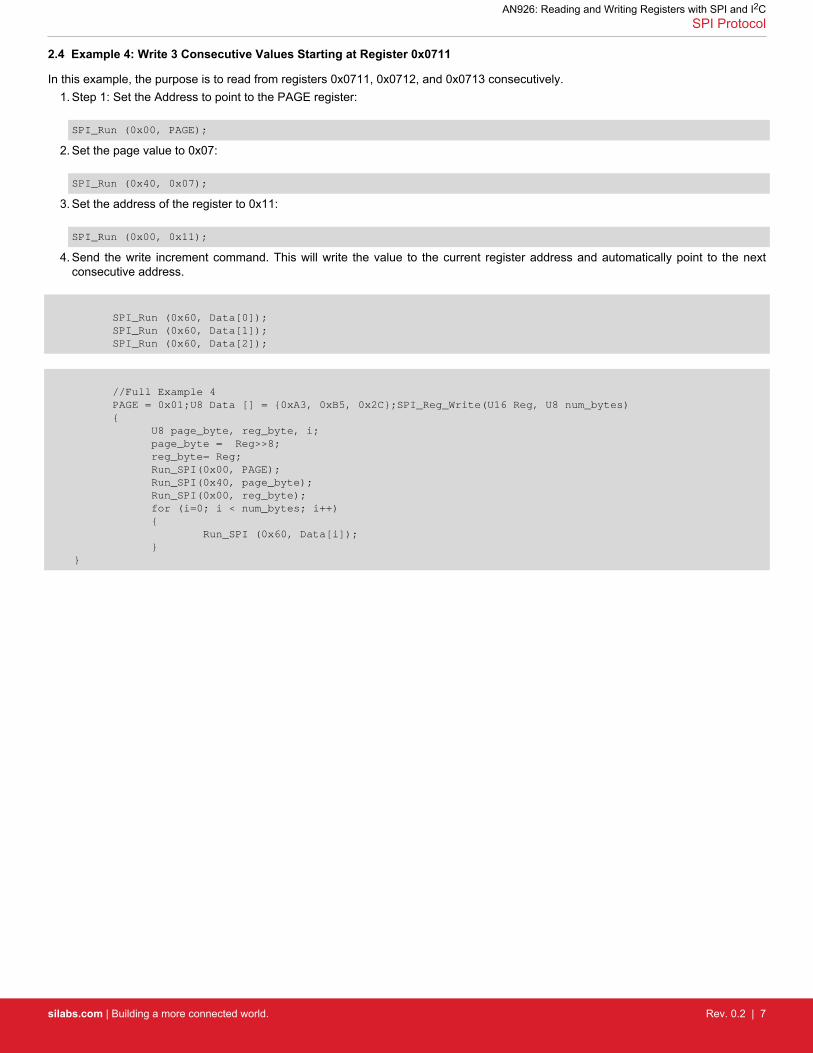
2.4 Example 4: Write 3 Consecutive Values Starting at Register 0x0711
In this example, the purpose is to read from registers 0x0711, 0x0712, and 0x0713 consecutively.1. Step 1: Set the Address to point to the PAGE register:
SPI_Run (0x00, PAGE);
2. Set the page value to 0x07:
SPI_Run (0x40, 0x07);
3. Set the address of the register to 0x11:
SPI_Run (0x00, 0x11);
4. Send the write increment command. This will write the value to the current register address and automatically point to the nextconsecutive address.
SPI_Run (0x60, Data[0]); SPI_Run (0x60, Data[1]); SPI_Run (0x60, Data[2]);
//Full Example 4 PAGE = 0x01;U8 Data [] = {0xA3, 0xB5, 0x2C};SPI_Reg_Write(U16 Reg, U8 num_bytes) { U8 page_byte, reg_byte, i; page_byte = Reg>>8; reg_byte= Reg; Run_SPI(0x00, PAGE); Run_SPI(0x40, page_byte); Run_SPI(0x00, reg_byte); for (i=0; i < num_bytes; i++) { Run_SPI (0x60, Data[i]); } }
AN926: Reading and Writing Registers with SPI and I2CSPI Protocol
silabs.com | Building a more connected world. Rev. 0.2 | 7
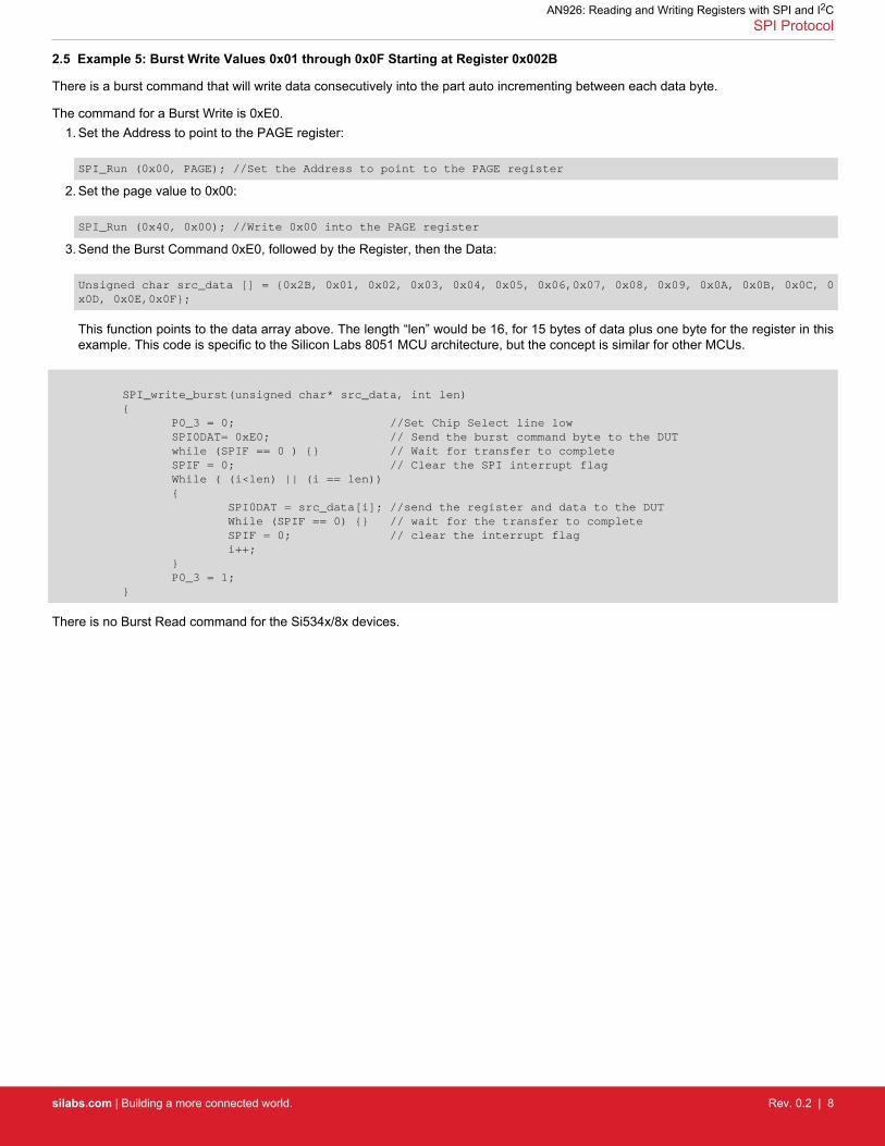
2.5 Example 5: Burst Write Values 0x01 through 0x0F Starting at Register 0x002B
There is a burst command that will write data consecutively into the part auto incrementing between each data byte.
The command for a Burst Write is 0xE0.1. Set the Address to point to the PAGE register:
SPI_Run (0x00, PAGE); //Set the Address to point to the PAGE register
2. Set the page value to 0x00:
SPI_Run (0x40, 0x00); //Write 0x00 into the PAGE register
3. Send the Burst Command 0xE0, followed by the Register, then the Data:
Unsigned char src_data [] = {0x2B, 0x01, 0x02, 0x03, 0x04, 0x05, 0x06,0x07, 0x08, 0x09, 0x0A, 0x0B, 0x0C, 0x0D, 0x0E,0x0F};
This function points to the data array above. The length “len” would be 16, for 15 bytes of data plus one byte for the register in thisexample. This code is specific to the Silicon Labs 8051 MCU architecture, but the concept is similar for other MCUs.
SPI_write_burst(unsigned char* src_data, int len) { P0_3 = 0; //Set Chip Select line low SPI0DAT= 0xE0; // Send the burst command byte to the DUT while (SPIF == 0 ) {} // Wait for transfer to complete SPIF = 0; // Clear the SPI interrupt flag While ( (i<len) || (i == len)) { SPI0DAT = src_data[i]; //send the register and data to the DUT While (SPIF == 0) {} // wait for the transfer to complete SPIF = 0; // clear the interrupt flag i++; } P0_3 = 1; }
There is no Burst Read command for the Si534x/8x devices.
AN926: Reading and Writing Registers with SPI and I2CSPI Protocol
silabs.com | Building a more connected world. Rev. 0.2 | 8
3. I2C Hardware Connections
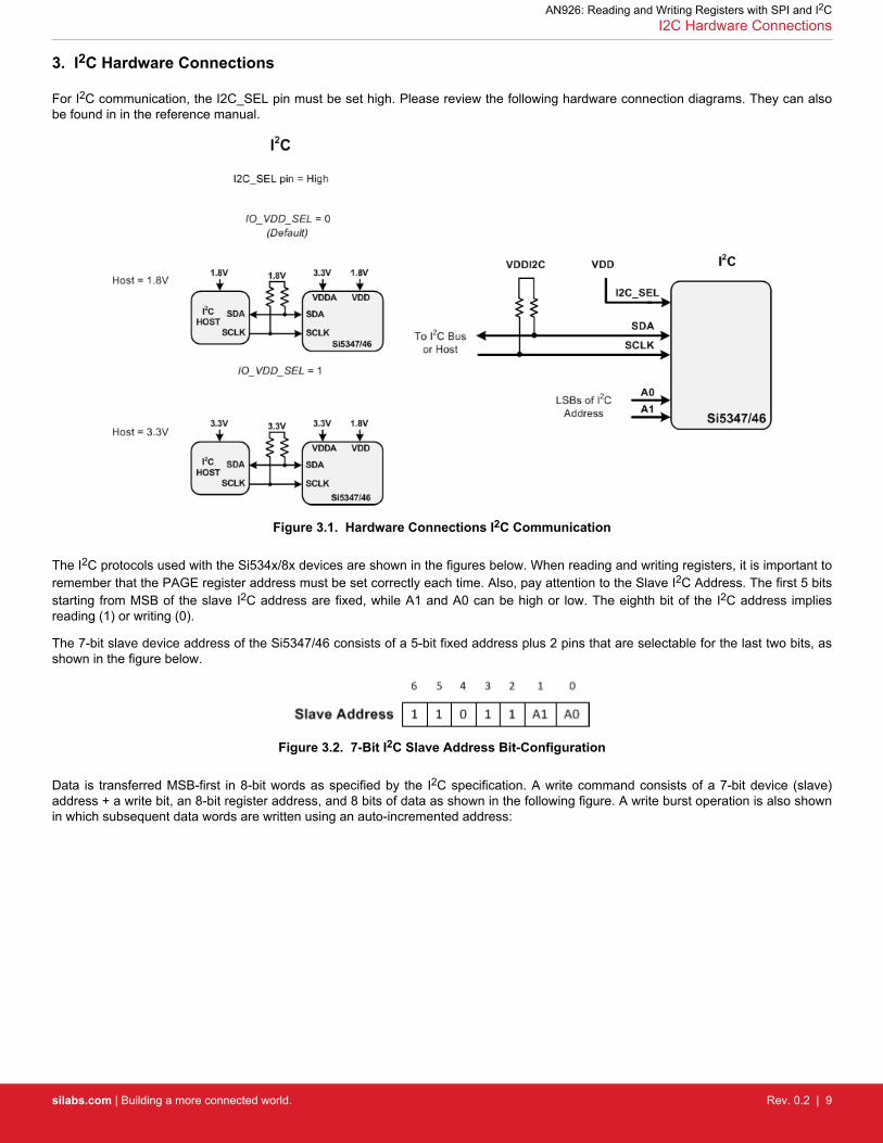
For I2C communication, the I2C_SEL pin must be set high. Please review the following hardware connection diagrams. They can alsobe found in in the reference manual.
Figure 3.1. Hardware Connections I2C Communication
The I2C protocols used with the Si534x/8x devices are shown in the figures below. When reading and writing registers, it is important toremember that the PAGE register address must be set correctly each time. Also, pay attention to the Slave I2C Address. The first 5 bitsstarting from MSB of the slave I2C address are fixed, while A1 and A0 can be high or low. The eighth bit of the I2C address impliesreading (1) or writing (0).
The 7-bit slave device address of the Si5347/46 consists of a 5-bit fixed address plus 2 pins that are selectable for the last two bits, asshown in the figure below.
Figure 3.2. 7-Bit I2C Slave Address Bit-Configuration
Data is transferred MSB-first in 8-bit words as specified by the I2C specification. A write command consists of a 7-bit device (slave)address + a write bit, an 8-bit register address, and 8 bits of data as shown in the following figure. A write burst operation is also shownin which subsequent data words are written using an auto-incremented address:
AN926: Reading and Writing Registers with SPI and I2CI2C Hardware Connections
silabs.com | Building a more connected world. Rev. 0.2 | 9
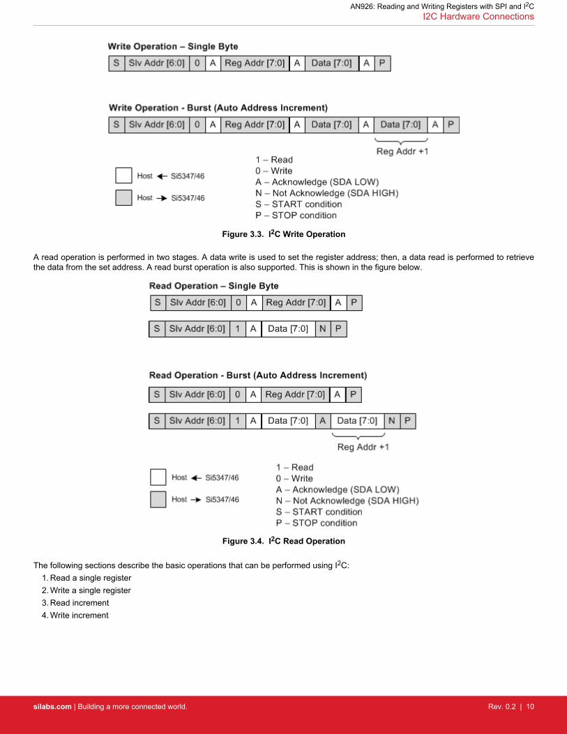
Figure 3.3. I2C Write Operation
A read operation is performed in two stages. A data write is used to set the register address; then, a data read is performed to retrievethe data from the set address. A read burst operation is also supported. This is shown in the figure below.
Figure 3.4. I2C Read Operation
The following sections describe the basic operations that can be performed using I2C:1. Read a single register2. Write a single register3. Read increment4. Write increment
AN926: Reading and Writing Registers with SPI and I2CI2C Hardware Connections
silabs.com | Building a more connected world. Rev. 0.2 | 10

3.1 Example 1: Read from Register 0x052A
In order to read register 0x052A, the first step is to write the PAGE register to 0x05. Then, write Register 0x2A, and, finally, read thedata out. Note that a read sequence always consists of first writing the register and then reading the data.
1. Write the Page Address (0x01) to a value of 0x05:
S/SlaveAddress/0/Ack/Reg_Address=0x01/Ack/Data=0x05/Ack/P
2. Read Address 0x2A.
The read sequence requires first writing the register, then reading out the data.
S/Slave Address/0/Ack/Reg_Address=0x2A/Ack/P //First Write the Register Address
S/Slave Address/1/Ack/DATA_RETURNED/N/P //Then Read out the Data
When reading a single byte from the device, the data length of 1 is passed to the I2C firmware to tell it to read one byte of data and thenstop.
3.2 Example 2: Write a Value of 0x23 to Register 0x03B9
The first step is to set the PAGE register to a value of 3, and then write a value of 23 into register 0xB9.1. Write the Page Address (0x01) to a value of 0x03:
S/SlaveAddress/0/Ack/Reg_Address=0x01/Ack/Data=0x03/Ack/P
2. Write a value of 0x23 into register 0xB9:
S/SlaveAddress/0/Ack/Reg_Address=0xB9/Ack/Data=0x23/Ack/P
When writing one byte of data, the firmware receives a data length instruction telling it to write in a single byte from the data passed in.
3.3 Example 3: Read 7 Values Starting from Register 0x0130
The first step is to set the PAGE register to 1; then, write the register address, and then read out the data, incrementing based on thelength passed in.
1. Write the Page Address (0x01) to a value of 0x01:
S/SlaveAddress/0/Ack/Reg_Address=0x01/Ack/Data=0x01/Ack/P
2. Read Address 0x30:
S/Slave Address/0/Ack/Reg_Address=0x30/Ack/P
S/Slave Address/1/Ack/DATA_RETURNED[0]/Ack/ DATA_RETURNED[1]/Ack/…DATA_RETURNED[6]/N/P
When reading multiple bytes from the device, the data length is passed to the I2C firmware to tell it to read the number of bytes of dataand then stop. The register address auto-increments as the data is incrementally read out.
3.4 Example 4: Write 8 Values Starting from Register 0x021C
After the page address is written, a multi-byte write is done by writing the register followed by all the data. The I2C driver will need toknow the length expected to continue incrementing and writing in all the values passed in.
1. Write the Page Address (0x01) to a value of 0x02:
S/SlaveAddress/0/Ack/Reg_Address=0x01/Ack/Data=0x03/Ack/P
2. Write a data value data[0],data[1],…data[7] starting at register 0x1C:
S/SlaveAddress/0/Ack/Reg_Address=0x1C/Ack/data[0]/Ack/data[1]/Ack/…data[7]/Ack/P
When writing multiple bytes from the device, the data length is passed to the I2C firmware to tell it to write the number of bytes of dataand then stop. The register address auto-increments as the data is incrementally written in.
AN926: Reading and Writing Registers with SPI and I2CI2C Hardware Connections
silabs.com | Building a more connected world. Rev. 0.2 | 11

http://www.silabs.com
Silicon Laboratories Inc.400 West Cesar ChavezAustin, TX 78701USA
ClockBuilder ProOne-click access to Timing tools, documentation, software, source code libraries & more. Available for Windows and iOS (CBGo only).
www.silabs.com/CBPro
Timing Portfoliowww.silabs.com/timing
SW/HWwww.silabs.com/CBPro
Qualitywww.silabs.com/quality
Support and Communitycommunity.silabs.com
DisclaimerSilicon Labs intends to provide customers with the latest, accurate, and in-depth documentation of all peripherals and modules available for system and software implementers using or intending to use the Silicon Labs products. Characterization data, available modules and peripherals, memory sizes and memory addresses refer to each specific device, and "Typical" parameters provided can and do vary in different applications. Application examples described herein are for illustrative purposes only. Silicon Labs reserves the right to make changes without further notice and limitation to product information, specifications, and descriptions herein, and does not give warranties as to the accuracy or completeness of the included information. Silicon Labs shall have no liability for the consequences of use of the information supplied herein. This document does not imply or express copyright licenses granted hereunder to design or fabricate any integrated circuits. The products are not designed or authorized to be used within any Life Support System without the specific written consent of Silicon Labs. A "Life Support System" is any product or system intended to support or sustain life and/or health, which, if it fails, can be reasonably expected to result in significant personal injury or death. Silicon Labs products are not designed or authorized for military applications. Silicon Labs products shall under no circumstances be used in weapons of mass destruction including (but not limited to) nuclear, biological or chemical weapons, or missiles capable of delivering such weapons.
Trademark InformationSilicon Laboratories Inc.® , Silicon Laboratories®, Silicon Labs®, SiLabs® and the Silicon Labs logo®, Bluegiga®, Bluegiga Logo®, Clockbuilder®, CMEMS®, DSPLL®, EFM®, EFM32®, EFR, Ember®, Energy Micro, Energy Micro logo and combinations thereof, "the world’s most energy friendly microcontrollers", Ember®, EZLink®, EZRadio®, EZRadioPRO®, Gecko®, ISOmodem®, Micrium, Precision32®, ProSLIC®, Simplicity Studio®, SiPHY®, Telegesis, the Telegesis Logo®, USBXpress®, Zentri, Z-Wave, and others are trademarks or registered trademarks of Silicon Labs. ARM, CORTEX, Cortex-M3 and THUMB are trademarks or registered trademarks of ARM Holdings. Keil is a registered trademark of ARM Limited. All other products or brand names mentioned herein are trademarks of their respective holders.