Embed Size (px)
Citation preview

November 2015 DocID028570 Rev 1 1/41
www.st.com
AN4783 Application note
Thermal effects and junction temperature evaluation of Power MOSFETs
Maurizio Melito, Antonino Gaito, Giuseppe Sorrentino
Introduction In modern power supply design, more and more attention is given to the electrical efficiency of the overall system and to the junction temperature of semiconductor devices, which handle the conversion of power to a usable form.
Among all semiconductor devices, the transistor is by far the most important category. Nearly all of them are three-pin devices (MOSFETs, BJTs, IGBTs) and unlike diodes, they have a driving section which makes them more sensitive to issues related to the interaction between power handling and the input signal. The aim of this application note is to illustrate the method to evaluate the thermal stress on power MOSFET devices when they are used in switch mode power supplies. By this computation and with the physics characteristics of the device, it is possible to predict the temperature reached inside the junction, and the allowable margin or heatsink required to assure that the system has a suitable thermal margin during operation. This approach is fundamental because correct computation allows more accurate evaluation of system lifetime and assures working operation within the SOA.

Contents AN4783
2/41 DocID028570 Rev 1
Contents
1 Description....................................................................................... 3
2 Thermal considerations .................................................................. 4
3 Rth as thermal resistance ............................................................... 5
4 Thermal factors ............................................................................... 7
5 Transfer heat modes ..................................................................... 15
5.1 MOSFET power losses ................................................................... 19
5.1.1 Conduction losses ............................................................................ 19
5.1.2 Switching losses ............................................................................... 24
6 Example 1 ...................................................................................... 31
7 Example 2 ...................................................................................... 36
8 References ..................................................................................... 39
9 Revision history ............................................................................ 40
AN4783 Description
DocID028570 Rev 1 3/41
1 Description
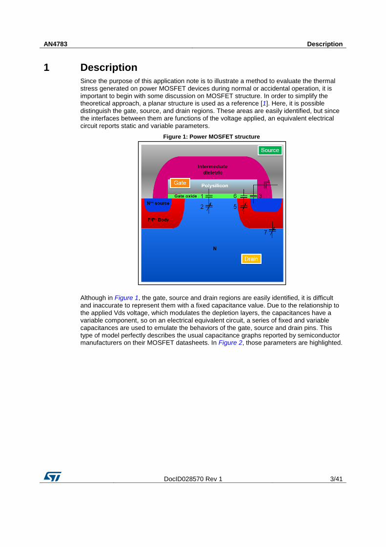
Since the purpose of this application note is to illustrate a method to evaluate the thermal stress generated on power MOSFET devices during normal or accidental operation, it is important to begin with some discussion on MOSFET structure. In order to simplify the theoretical approach, a planar structure is used as a reference [1]. Here, it is possible distinguish the gate, source, and drain regions. These areas are easily identified, but since the interfaces between them are functions of the voltage applied, an equivalent electrical circuit reports static and variable parameters.
Figure 1: Power MOSFET structure
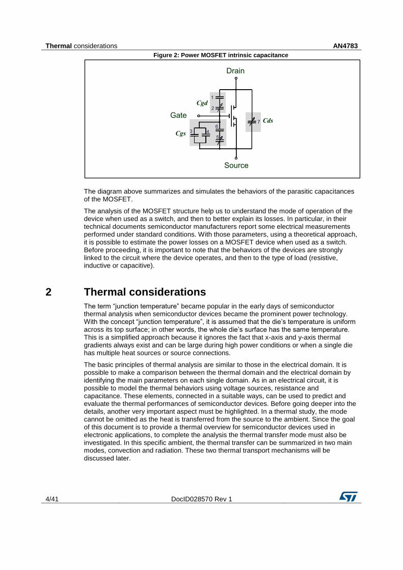
Although in Figure 1, the gate, source and drain regions are easily identified, it is difficult and inaccurate to represent them with a fixed capacitance value. Due to the relationship to the applied Vds voltage, which modulates the depletion layers, the capacitances have a variable component, so on an electrical equivalent circuit, a series of fixed and variable capacitances are used to emulate the behaviors of the gate, source and drain pins. This type of model perfectly describes the usual capacitance graphs reported by semiconductor manufacturers on their MOSFET datasheets. In Figure 2, those parameters are highlighted.
Thermal considerations AN4783
4/41 DocID028570 Rev 1
Figure 2: Power MOSFET intrinsic capacitance
The diagram above summarizes and simulates the behaviors of the parasitic capacitances of the MOSFET.
The analysis of the MOSFET structure help us to understand the mode of operation of the device when used as a switch, and then to better explain its losses. In particular, in their technical documents semiconductor manufacturers report some electrical measurements performed under standard conditions. With those parameters, using a theoretical approach, it is possible to estimate the power losses on a MOSFET device when used as a switch. Before proceeding, it is important to note that the behaviors of the devices are strongly linked to the circuit where the device operates, and then to the type of load (resistive, inductive or capacitive).
2 Thermal considerations
The term “junction temperature” became popular in the early days of semiconductor thermal analysis when semiconductor devices became the prominent power technology. With the concept “junction temperature”, it is assumed that the die’s temperature is uniform across its top surface; in other words, the whole die’s surface has the same temperature. This is a simplified approach because it ignores the fact that x-axis and y-axis thermal gradients always exist and can be large during high power conditions or when a single die has multiple heat sources or source connections.
The basic principles of thermal analysis are similar to those in the electrical domain. It is possible to make a comparison between the thermal domain and the electrical domain by identifying the main parameters on each single domain. As in an electrical circuit, it is possible to model the thermal behaviors using voltage sources, resistance and capacitance. These elements, connected in a suitable ways, can be used to predict and evaluate the thermal performances of semiconductor devices. Before going deeper into the details, another very important aspect must be highlighted. In a thermal study, the mode cannot be omitted as the heat is transferred from the source to the ambient. Since the goal of this document is to provide a thermal overview for semiconductor devices used in electronic applications, to complete the analysis the thermal transfer mode must also be investigated. In this specific ambient, the thermal transfer can be summarized in two main modes, convection and radiation. These two thermal transport mechanisms will be discussed later.
AN4783 Rth as thermal resistance
DocID028570 Rev 1 5/41
3 Rth as thermal resistance
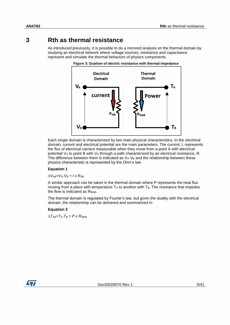
As introduced previously, it is possible to do a mirrored analysis on the thermal domain by studying an electrical network where voltage sources, resistance and capacitance represent and simulate the thermal behaviors of physics components.
Figure 3: Dualism of electric resistance with thermal impedance
Each single domain is characterized by two main physical characteristics. In the electrical domain, current and electrical potential are the main parameters. The current, I, represents the flux of electrical carriers measurable when they move from a point A with electrical potential VA to point B with VB through a path characterized by an electrical resistance, R. The difference between them is indicated as VA-VB and the relationship between these physics characteristic is represented by the Ohm’s law.
Equation 1
∆VAB=VA-VB = I x RAB
A similar approach can be taken in the thermal domain where P represents the heat flux moving from a place with temperature TA to another with TB. The resistance that impedes the flow is indicated as RƟAB.
The thermal domain is regulated by Fourier’s law, but given the duality with the electrical domain, the relationship can be delivered and summarized in:
Equation 2
∆TAB=TA-TB = P x RƟAB
Rth as thermal resistance AN4783
6/41 DocID028570 Rev 1
The following table summarizes and compares the physics characteristics on the two domains.
Table 1: Physics characteristics of the two domains
Electrical domain Thermal domain
Variable Symbol Unit Variable Symbol Unit
Current I A Thermal power PD W
Voltage V V Temperature TX °C
Electrical resistance R Ω Thermal resistance RƟXY °C/W
Electrical capacitance C F Thermal capacitance CƟ J/°C
∆VAB=I x RAB ∆TAB=PƟ x RƟAB
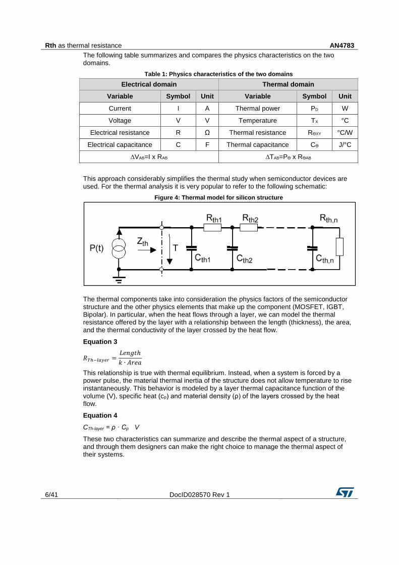
This approach considerably simplifies the thermal study when semiconductor devices are used. For the thermal analysis it is very popular to refer to the following schematic:
Figure 4: Thermal model for silicon structure
The thermal components take into consideration the physics factors of the semiconductor structure and the other physics elements that make up the component (MOSFET, IGBT, Bipolar). In particular, when the heat flows through a layer, we can model the thermal resistance offered by the layer with a relationship between the length (thickness), the area, and the thermal conductivity of the layer crossed by the heat flow.
Equation 3
𝑅𝑇ℎ−𝑙𝑎𝑦𝑒𝑟 =𝐿𝑒𝑛𝑔𝑡ℎ
𝑘 ∙ 𝐴𝑟𝑒𝑎
This relationship is true with thermal equilibrium. Instead, when a system is forced by a power pulse, the material thermal inertia of the structure does not allow temperature to rise instantaneously. This behavior is modeled by a layer thermal capacitance function of the volume (V), specific heat (cp) and material density (ρ) of the layers crossed by the heat flow.
Equation 4
CTh-layer = ρ · Cp · V
These two characteristics can summarize and describe the thermal aspect of a structure, and through them designers can make the right choice to manage the thermal aspect of their systems.
AN4783 Thermal factors
DocID028570 Rev 1 7/41
4 Thermal factors
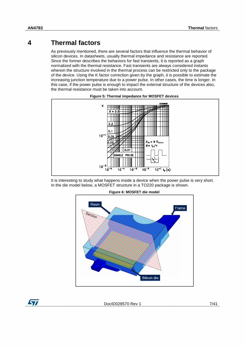
As previously mentioned, there are several factors that influence the thermal behavior of silicon devices. In datasheets, usually thermal impedance and resistance are reported. Since the former describes the behaviors for fast transients, it is reported as a graph normalized with the thermal resistance. Fast transients are always considered instants wherein the structure involved in the thermal process can be restricted only to the package of the device. Using the K factor correction given by the graph, it is possible to estimate the increasing junction temperature due to a power pulse. In other cases, the time is longer. In this case, if the power pulse is enough to impact the external structure of the devices also, the thermal resistance must be taken into account.
Figure 5: Thermal impedance for MOSFET devices
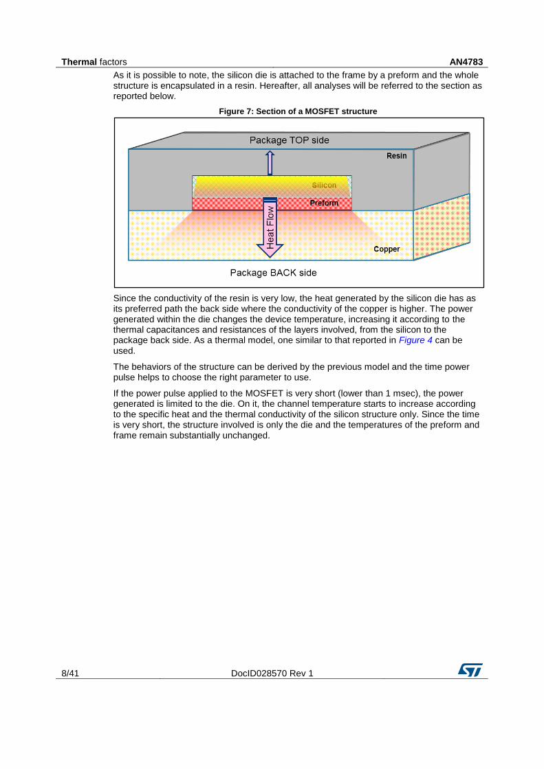
It is interesting to study what happens inside a device when the power pulse is very short. In the die model below, a MOSFET structure in a TO220 package is shown.
Figure 6: MOSFET die model
Thermal factors AN4783
8/41 DocID028570 Rev 1
As it is possible to note, the silicon die is attached to the frame by a preform and the whole structure is encapsulated in a resin. Hereafter, all analyses will be referred to the section as reported below.
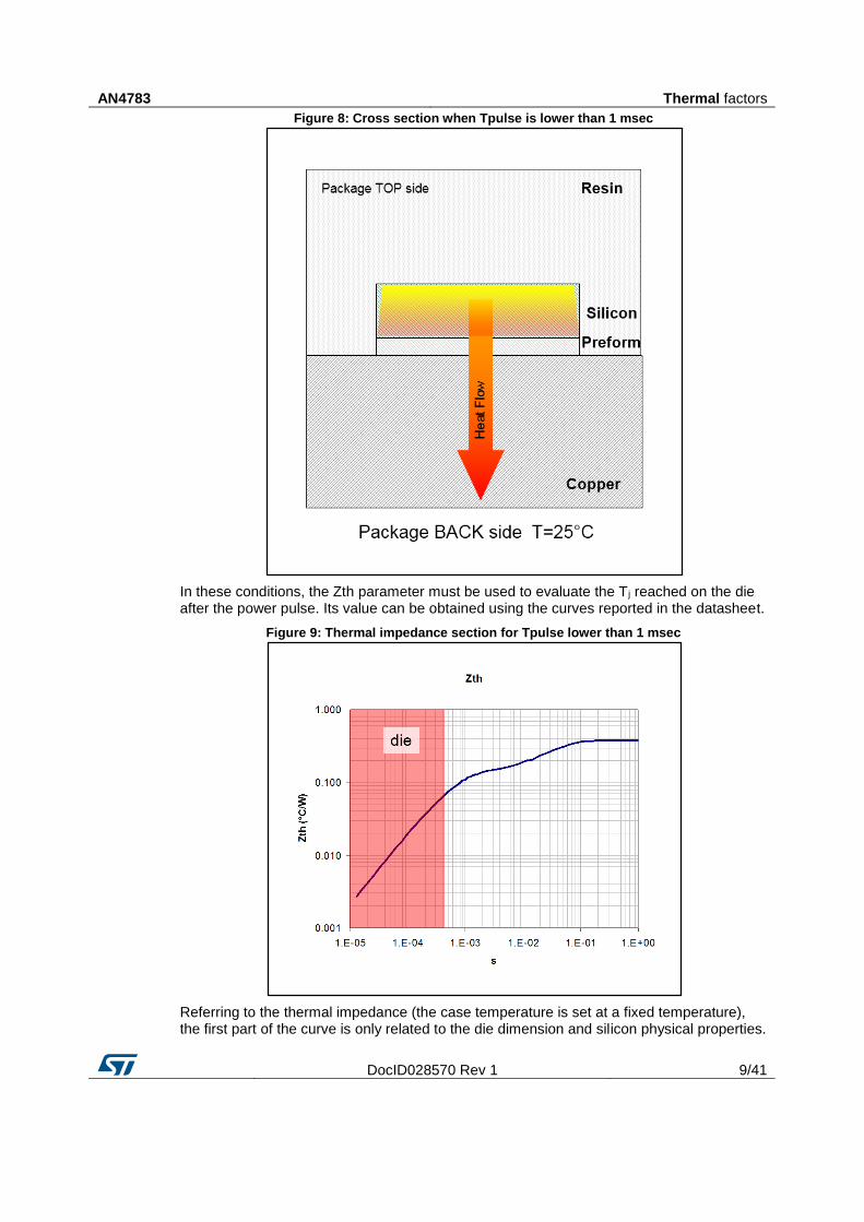
Figure 7: Section of a MOSFET structure
Since the conductivity of the resin is very low, the heat generated by the silicon die has as its preferred path the back side where the conductivity of the copper is higher. The power generated within the die changes the device temperature, increasing it according to the thermal capacitances and resistances of the layers involved, from the silicon to the package back side. As a thermal model, one similar to that reported in Figure 4 can be used.
The behaviors of the structure can be derived by the previous model and the time power pulse helps to choose the right parameter to use.
If the power pulse applied to the MOSFET is very short (lower than 1 msec), the power generated is limited to the die. On it, the channel temperature starts to increase according to the specific heat and the thermal conductivity of the silicon structure only. Since the time is very short, the structure involved is only the die and the temperatures of the preform and frame remain substantially unchanged.
AN4783 Thermal factors
DocID028570 Rev 1 9/41
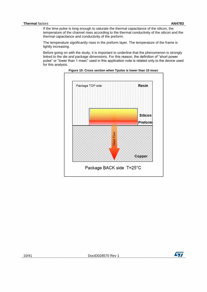
Figure 8: Cross section when Tpulse is lower than 1 msec
In these conditions, the Zth parameter must be used to evaluate the Tj reached on the die after the power pulse. Its value can be obtained using the curves reported in the datasheet.
Figure 9: Thermal impedance section for Tpulse lower than 1 msec
Referring to the thermal impedance (the case temperature is set at a fixed temperature), the first part of the curve is only related to the die dimension and silicon physical properties.
Thermal factors AN4783
10/41 DocID028570 Rev 1
If the time pulse is long enough to saturate the thermal capacitance of the silicon, the temperature of the channel rises according to the thermal conductivity of the silicon and the thermal capacitance and conductivity of the preform.
The temperature significantly rises in the preform layer. The temperature of the frame is lightly increasing.
Before going on with the study, it is important to underline that the phenomenon is strongly linked to the die and package dimensions. For this reason, the definition of “short power pulse” or “lower than 1 msec” used in this application note is related only to the device used for this analysis.
Figure 10: Cross section when Tpulse is lower than 10 msec
AN4783 Thermal factors
DocID028570 Rev 1 11/41
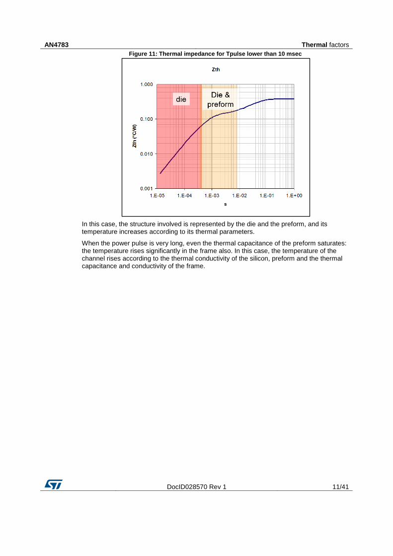
Figure 11: Thermal impedance for Tpulse lower than 10 msec
In this case, the structure involved is represented by the die and the preform, and its temperature increases according to its thermal parameters.
When the power pulse is very long, even the thermal capacitance of the preform saturates: the temperature rises significantly in the frame also. In this case, the temperature of the channel rises according to the thermal conductivity of the silicon, preform and the thermal capacitance and conductivity of the frame.
Thermal factors AN4783
12/41 DocID028570 Rev 1
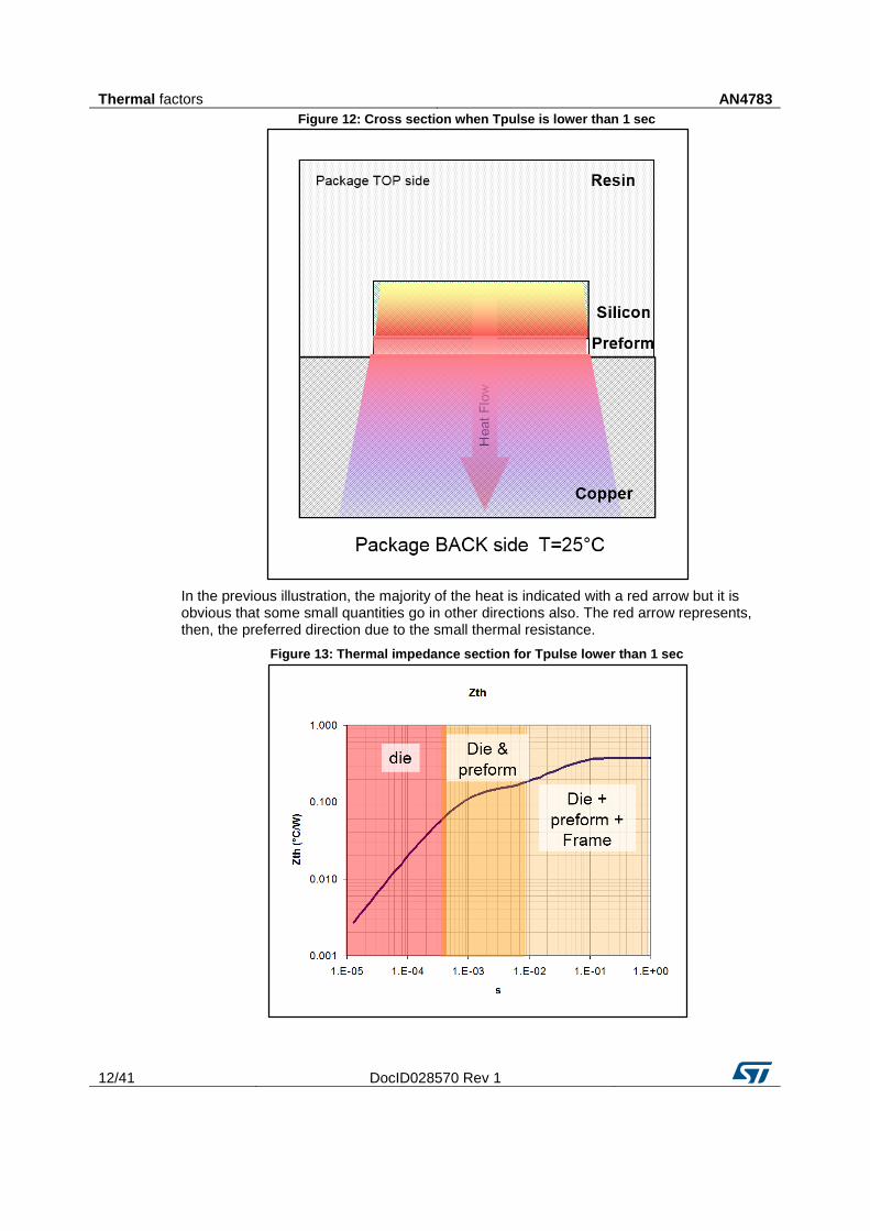
Figure 12: Cross section when Tpulse is lower than 1 sec
In the previous illustration, the majority of the heat is indicated with a red arrow but it is obvious that some small quantities go in other directions also. The red arrow represents, then, the preferred direction due to the small thermal resistance.
Figure 13: Thermal impedance section for Tpulse lower than 1 sec
AN4783 Thermal factors
DocID028570 Rev 1 13/41
When the thermal capacitance of the frame saturates also, thermal equilibrium is reached and the total thermal resistance depends on all the layers of the package.
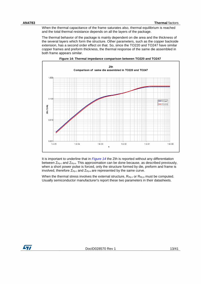
The thermal behavior of the package is mainly dependent on die area and the thickness of the several layers which form the structure. Other parameters, such as the copper backside extension, has a second order effect on that. So, since the TO220 and TO247 have similar copper frames and preform thickness, the thermal response of the same die assembled in both frame appears similar.
Figure 14: Thermal impedance comparison between TO220 and TO247
It is important to underline that in Figure 14 the Zth is reported without any differentiation between Zthj-c and Zthj-a. This approximation can be done because, as described previously, when a short power pulse is forced, only the structure formed by die, preform and frame is involved, therefore Zthj-c and Zthj-a are represented by the same curve.
When the thermal stress involves the external structure, Rthj-c or Rthj-a must be computed. Usually semiconductor manufacturer's report these two parameters in their datasheets.
Thermal factors AN4783
14/41 DocID028570 Rev 1
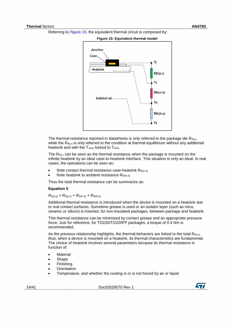
Referring to Figure 15, the equivalent thermal circuit is composed by:
Figure 15: Equivalent thermal model
The thermal resistance reported in datasheets is only referred to the package die Rthj-c, while the Rthj-a is only referred to the condition at thermal equilibrium without any additional heatsink and with the Tcase locked to Tamb.
The Rthj-c can be seen as the thermal resistance when the package is mounted on the infinite heatsink by an ideal case-to-heatsink interface. This situation is only an ideal. In real cases, the operations can be seen as:
finite contact thermal resistance case-heatsink Rth(c-h)
finite heatsink to ambient resistance Rth(h-a)
Thus the total thermal resistance can be summarize as:
Equation 5
Rth(j-a) = Rth(j-c) + Rth(c-h) + Rth(h-a)
Additional thermal resistance is introduced when the device is mounted on a heatsink due to real contact surfaces. Sometime grease is used or an isolator layer (such as mica, ceramic or silicon) is inserted, for non-insulated packages, between package and heatsink.
This thermal resistance can be minimized by contact grease and an appropriate pressure force. Just for reference, for TO220/TO220FP packages, a torque of 0.4 Nm is recommended.
As the previous relationship highlights, the thermal behaviors are linked to the total Rthj-a, thus, when a device is mounted on a heatsink, its thermal characteristics are fundamental. The choice of heatsink involves several parameters because its thermal resistance is function of:
Material
Shape
Finishing
Orientation
Temperature, and whether the cooling is or is not forced by air or liquid
AN4783 Transfer heat modes
DocID028570 Rev 1 15/41
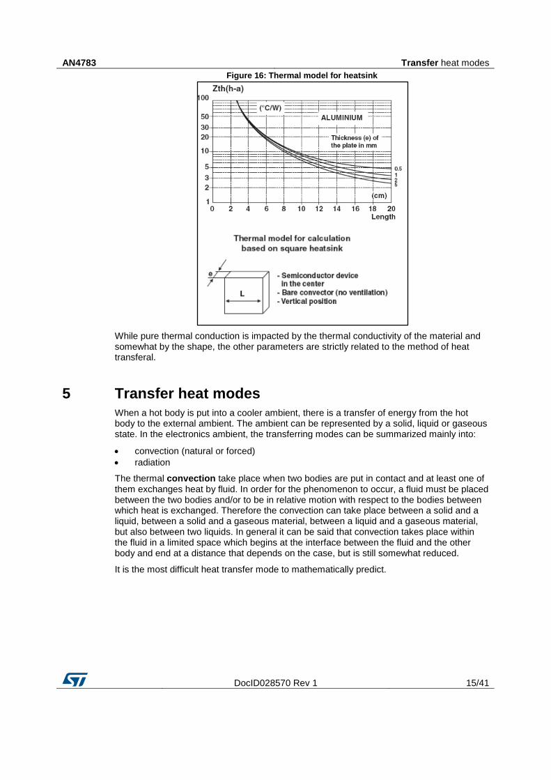
Figure 16: Thermal model for heatsink
While pure thermal conduction is impacted by the thermal conductivity of the material and somewhat by the shape, the other parameters are strictly related to the method of heat transferal.
5 Transfer heat modes
When a hot body is put into a cooler ambient, there is a transfer of energy from the hot body to the external ambient. The ambient can be represented by a solid, liquid or gaseous state. In the electronics ambient, the transferring modes can be summarized mainly into:
convection (natural or forced)
radiation
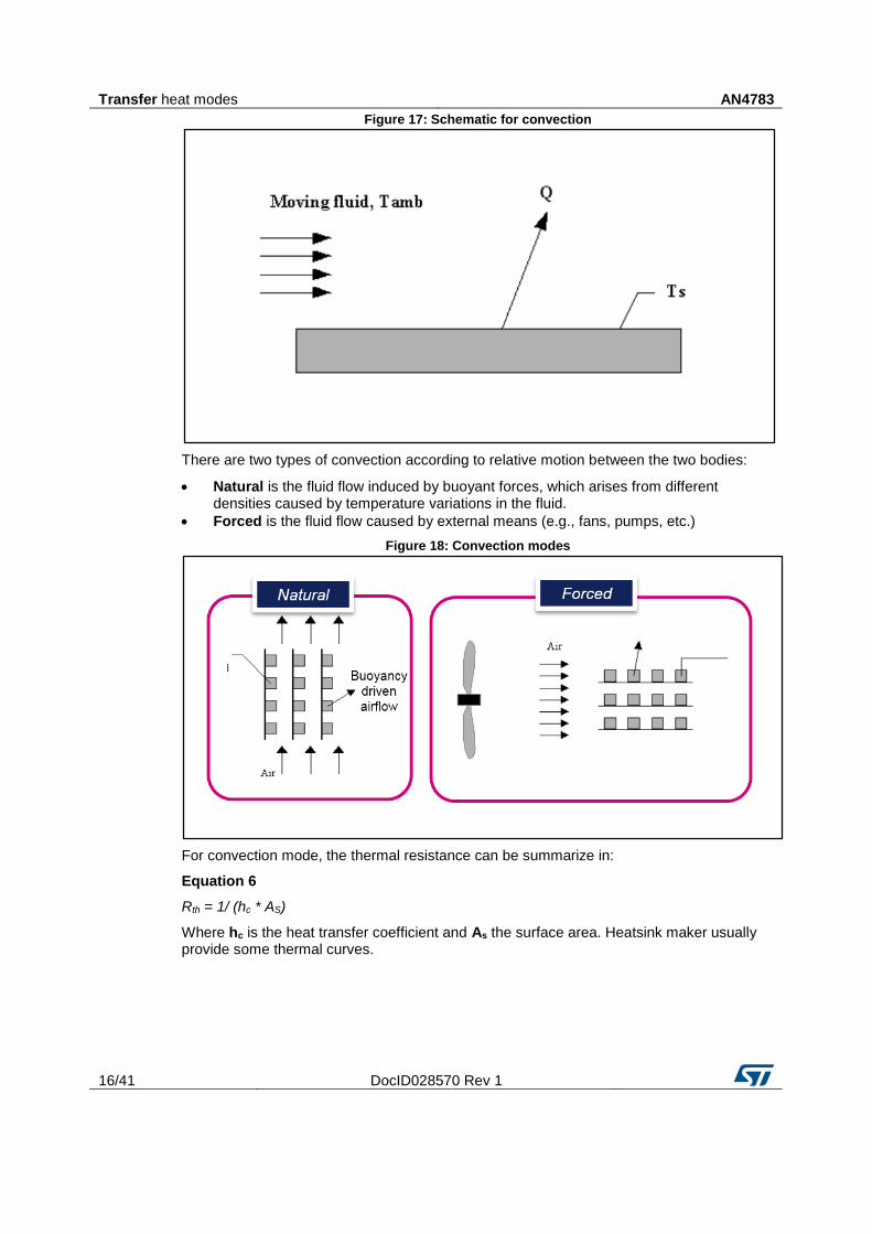
The thermal convection take place when two bodies are put in contact and at least one of them exchanges heat by fluid. In order for the phenomenon to occur, a fluid must be placed between the two bodies and/or to be in relative motion with respect to the bodies between which heat is exchanged. Therefore the convection can take place between a solid and a liquid, between a solid and a gaseous material, between a liquid and a gaseous material, but also between two liquids. In general it can be said that convection takes place within the fluid in a limited space which begins at the interface between the fluid and the other body and end at a distance that depends on the case, but is still somewhat reduced.
It is the most difficult heat transfer mode to mathematically predict.
Transfer heat modes AN4783
16/41 DocID028570 Rev 1
Figure 17: Schematic for convection
There are two types of convection according to relative motion between the two bodies:
Natural is the fluid flow induced by buoyant forces, which arises from different densities caused by temperature variations in the fluid.
Forced is the fluid flow caused by external means (e.g., fans, pumps, etc.)
Figure 18: Convection modes
For convection mode, the thermal resistance can be summarize in:
Equation 6
Rth = 1/ (hc * AS)
Where hc is the heat transfer coefficient and As the surface area. Heatsink maker usually provide some thermal curves.
AN4783 Transfer heat modes
DocID028570 Rev 1 17/41
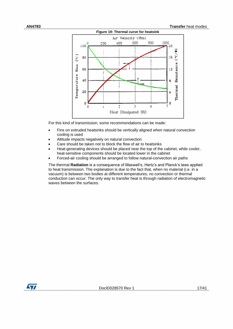
Figure 19: Thermal curve for heatsink
For this kind of transmission, some recommendations can be made:
Fins on extruded heatsinks should be vertically aligned when natural convection cooling is used
Altitude impacts negatively on natural convection
Care should be taken not to block the flow of air to heatsinks
Heat-generating devices should be placed near the top of the cabinet, while cooler, heat-sensitive components should be located lower in the cabinet
Forced-air cooling should be arranged to follow natural-convection air paths
The thermal Radiation is a consequence of Maxwell’s, Hertz’s and Planck’s laws applied to heat transmission. The explanation is due to the fact that, when no material (i.e. in a vacuum) is between two bodies at different temperatures, no convection or thermal conduction can occur. The only way to transfer heat is through radiation of electromagnetic waves between the surfaces.
Transfer heat modes AN4783
18/41 DocID028570 Rev 1
Figure 20: Schematic for radiation
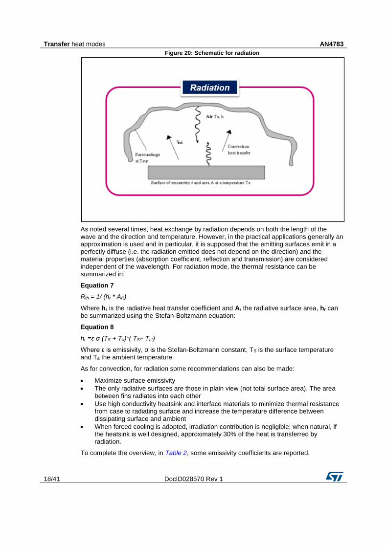
As noted several times, heat exchange by radiation depends on both the length of the wave and the direction and temperature. However, in the practical applications generally an approximation is used and in particular, it is supposed that the emitting surfaces emit in a perfectly diffuse (i.e. the radiation emitted does not depend on the direction) and the material properties (absorption coefficient, reflection and transmission) are considered independent of the wavelength. For radiation mode, the thermal resistance can be summarized in:
Equation 7
Rth = 1/ (hr * AR)
Where hr is the radiative heat transfer coefficient and Ar the radiative surface area, hr can be summarized using the Stefan-Boltzmann equation:
Equation 8
hr =ε σ (TS + Ta)*( TS²- Ta²)
Where ε is emissivity, σ is the Stefan-Boltzmann constant, TS is the surface temperature and Ta the ambient temperature.
As for convection, for radiation some recommendations can also be made:
Maximize surface emissivity
The only radiative surfaces are those in plain view (not total surface area). The area between fins radiates into each other
Use high conductivity heatsink and interface materials to minimize thermal resistance from case to radiating surface and increase the temperature difference between dissipating surface and ambient
When forced cooling is adopted, irradiation contribution is negligible; when natural, if the heatsink is well designed, approximately 30% of the heat is transferred by radiation.
To complete the overview, in Table 2, some emissivity coefficients are reported.

AN4783 Transfer heat modes
DocID028570 Rev 1 19/41
Table 2: Emissivity coefficients
Material and finish Emissivity
Aluminum - polished 0.04
Aluminum - rough 0.06
Aluminum - anodized (any color) 0.8
Copper - commercial polished 0.03
Copper - machined 0.07
Copper - thick oxide coating 0.78
Steel - rolled sheet 0.55
Steel - oxidized 0.78
Stainless steel - alloy 316 0.28
Nickel plate - dull finish 0.11
Silver - polished 0.02
Tin - bright 0.04
Paints & lacquers - any color - flat finish 0.94
Paints & lacquers - any color - gloss finish 0.89
5.1 MOSFET power losses
When a power MOSFET is used as a switch in an electronic application, it is submitted to thermal stress due to the electrical power dissipated on it. In order to design a robust project, designers evaluate the power losses starting from the specifics of the electrical application, topologies implemented, and modes to dissipate the heat. This study allows a choice of the right components to operate in a safe manner. By restricting the area of the power losses in the switch device, the power losses dissipated inside the device during operation can be categorized in two main classes:
Conduction losses (related to the ohmic characteristics of the device)
Switching losses divided into:
Turn-on/turn-off losses
Output capacitance stored energy loss
Gate driving loss
Freewheeling diode additional losses
Thus the total losses can be written as:
Equation 9
Ptot = Pcond + Psw + PCoss +Pdriving+Pdiode
Each single contribution is linked to a specific working operation, then we analyze them.
5.1.1 Conduction losses
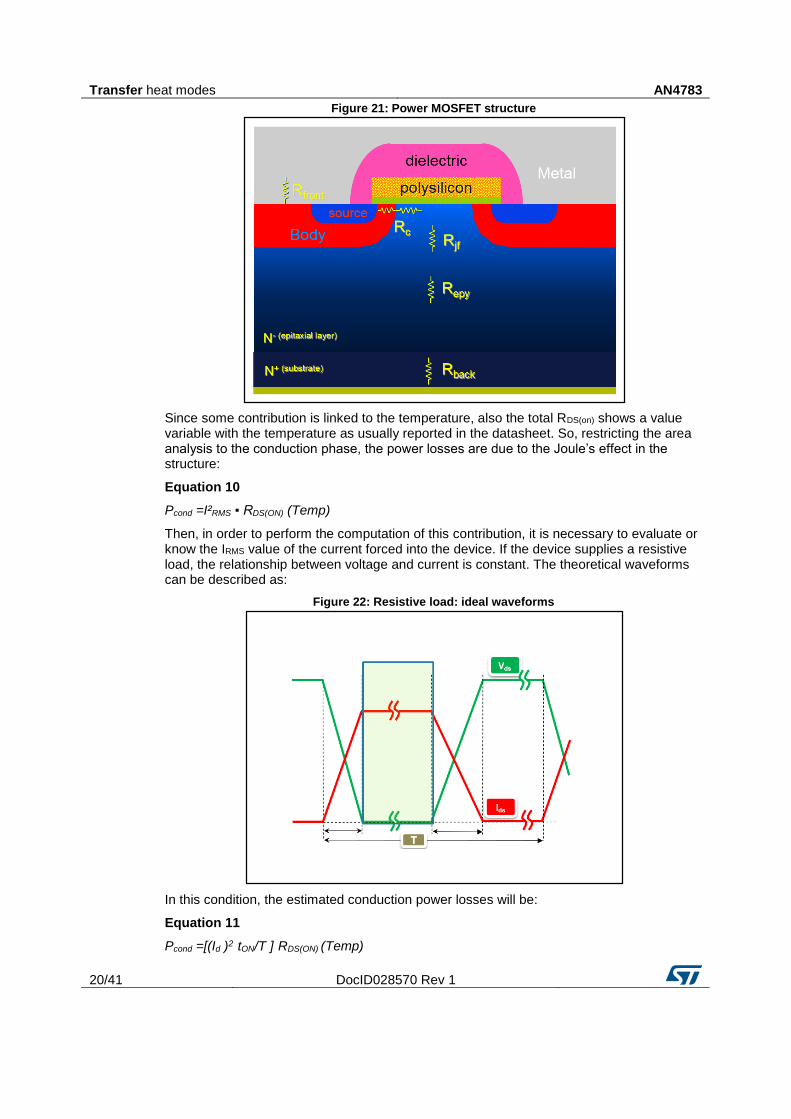
When the device is fully on, the only electrical resistance is represented by the resistance of the structure. This resistance is due to many contributions, as Figure 21 shows:
Transfer heat modes AN4783
20/41 DocID028570 Rev 1
Figure 21: Power MOSFET structure
Since some contribution is linked to the temperature, also the total RDS(on) shows a value variable with the temperature as usually reported in the datasheet. So, restricting the area analysis to the conduction phase, the power losses are due to the Joule’s effect in the structure:
Equation 10
Pcond =I²RMS ▪ RDS(ON) (Temp)
Then, in order to perform the computation of this contribution, it is necessary to evaluate or know the IRMS value of the current forced into the device. If the device supplies a resistive load, the relationship between voltage and current is constant. The theoretical waveforms can be described as:
Figure 22: Resistive load: ideal waveforms
In this condition, the estimated conduction power losses will be:
Equation 11
Pcond =[(Id )2·tON/T ]·RDS(ON) (Temp)

AN4783 Transfer heat modes
DocID028570 Rev 1 21/41
If the system supplies an inductive load, the current waveform is delayed compared to the voltage waveform. Furthermore, CCM or DCM perform in different ways. The following relationship summarizes the whole condition referring to Figure 23.
Figure 23: Inductive load: ideal waveforms
Ia is the current value at turn-on while Ib is thevalue at turn-off. In DCM mode, Ia is equal to zero, therefore:
Equation 12a
Pcond =1/3 · I²b · RDS(ON) (Temp) · tON /T
If the system operates in CCM, the new relationship will be:
Equation 12b
Pcond =1/3 · (I²a+I²b+ Ia·Ib) · RDS(ON) (Temp) · tON /T
The above formulas allow evaluation of the power losses due to the Joule’s effect on the structure.
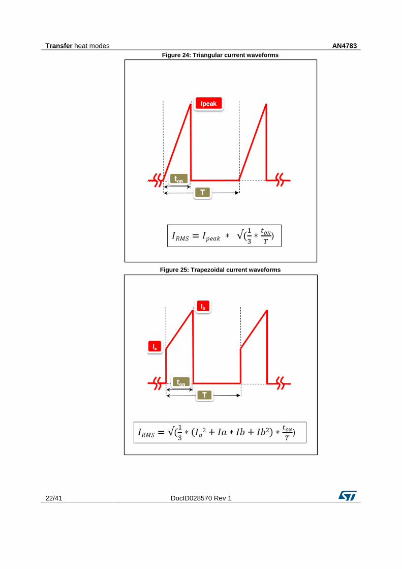
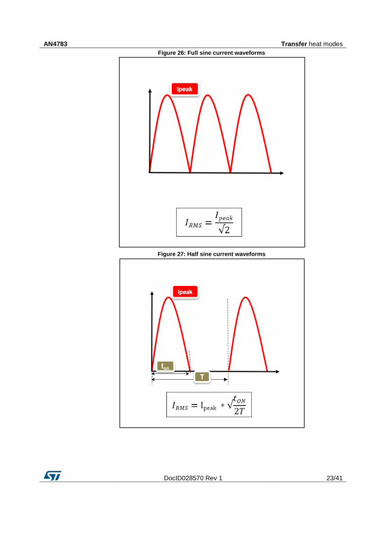
To complete the overview, some typical current waveforms and the relative IRMS values are reported.
Transfer heat modes AN4783
22/41 DocID028570 Rev 1
Figure 24: Triangular current waveforms
Figure 25: Trapezoidal current waveforms
AN4783 Transfer heat modes
DocID028570 Rev 1 23/41
Figure 26: Full sine current waveforms
Figure 27: Half sine current waveforms
Transfer heat modes AN4783
24/41 DocID028570 Rev 1
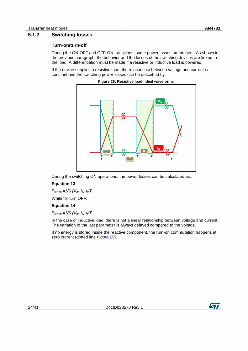
5.1.2 Switching losses
Turn-on/turn-off
During the ON-OFF and OFF-ON transitions, some power losses are present. As shown in the previous paragraph, the behavior and the losses of the switching devices are linked to the load. A differentiation must be made if a resistive or inductive load is powered.
If the device supplies a resistive load, the relationship between voltage and current is constant and the switching power losses can be described by:
Figure 28: Resistive load: ideal waveforms
During the switching ON operations, the power losses can be calculated as:
Equation 13
Psw(on)=1/6·(Vds·Id)·tr/T
While for turn OFF:
Equation 14
Psw(off)=1/6·(Vds·Id)·tf/T
In the case of inductive load, there is not a linear relationship between voltage and current. The variation of the last parameter is always delayed compared to the voltage.
If no energy is stored inside the reactive component, the turn-on commutation happens at zero current (dotted line Figure 29).
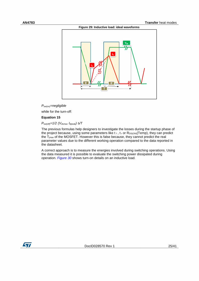
AN4783 Transfer heat modes
DocID028570 Rev 1 25/41
Figure 29: Inductive load: ideal waveforms
Psw(on)=negligible
while for the turn-off:
Equation 15
Psw(off)=1/2·(Vdsmax·Idpeak)·tf/T
The previous formulas help designers to investigate the losses during the startup phase of the project because, using some parameters like t f , t r or RDS(ON)(Temp), they can predict the Tjmax of the MOSFET. However this is false because, they cannot predict the real parameter values due to the different working operation compared to the data reported in the datasheet.
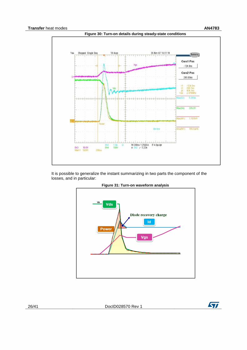
A correct approach is to measure the energies involved during switching operations. Using the data measured it is possible to evaluate the switching power dissipated during operation. Figure 30 shows turn-on details on an inductive load.
Transfer heat modes AN4783
26/41 DocID028570 Rev 1
Figure 30: Turn-on details during steady-state conditions
It is possible to generalize the instant summarizing in two parts the component of the losses, and in particular:
Figure 31: Turn-on waveform analysis
AN4783 Transfer heat modes
DocID028570 Rev 1 27/41
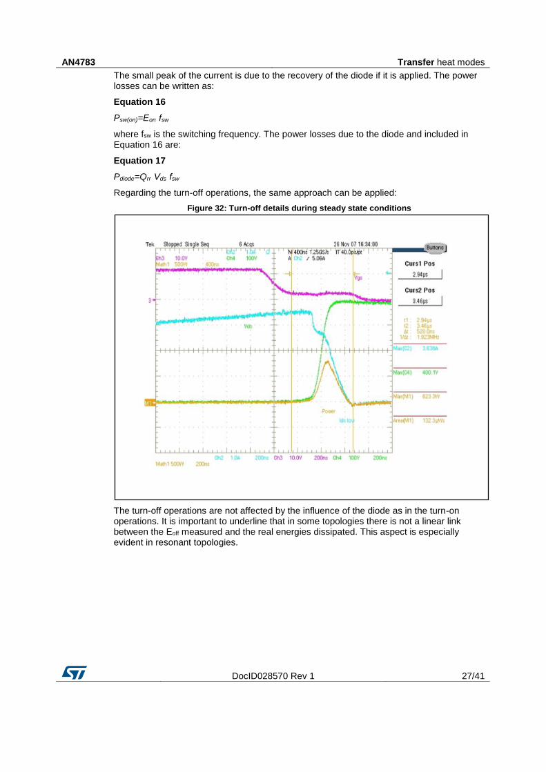
The small peak of the current is due to the recovery of the diode if it is applied. The power losses can be written as:
Equation 16
Psw(on)=Eon·fsw
where fsw is the switching frequency. The power losses due to the diode and included in Equation 16 are:
Equation 17
Pdiode=Qrr·Vds·fsw
Regarding the turn-off operations, the same approach can be applied:
Figure 32: Turn-off details during steady state conditions
The turn-off operations are not affected by the influence of the diode as in the turn-on operations. It is important to underline that in some topologies there is not a linear link between the Eoff measured and the real energies dissipated. This aspect is especially evident in resonant topologies.
Transfer heat modes AN4783
28/41 DocID028570 Rev 1
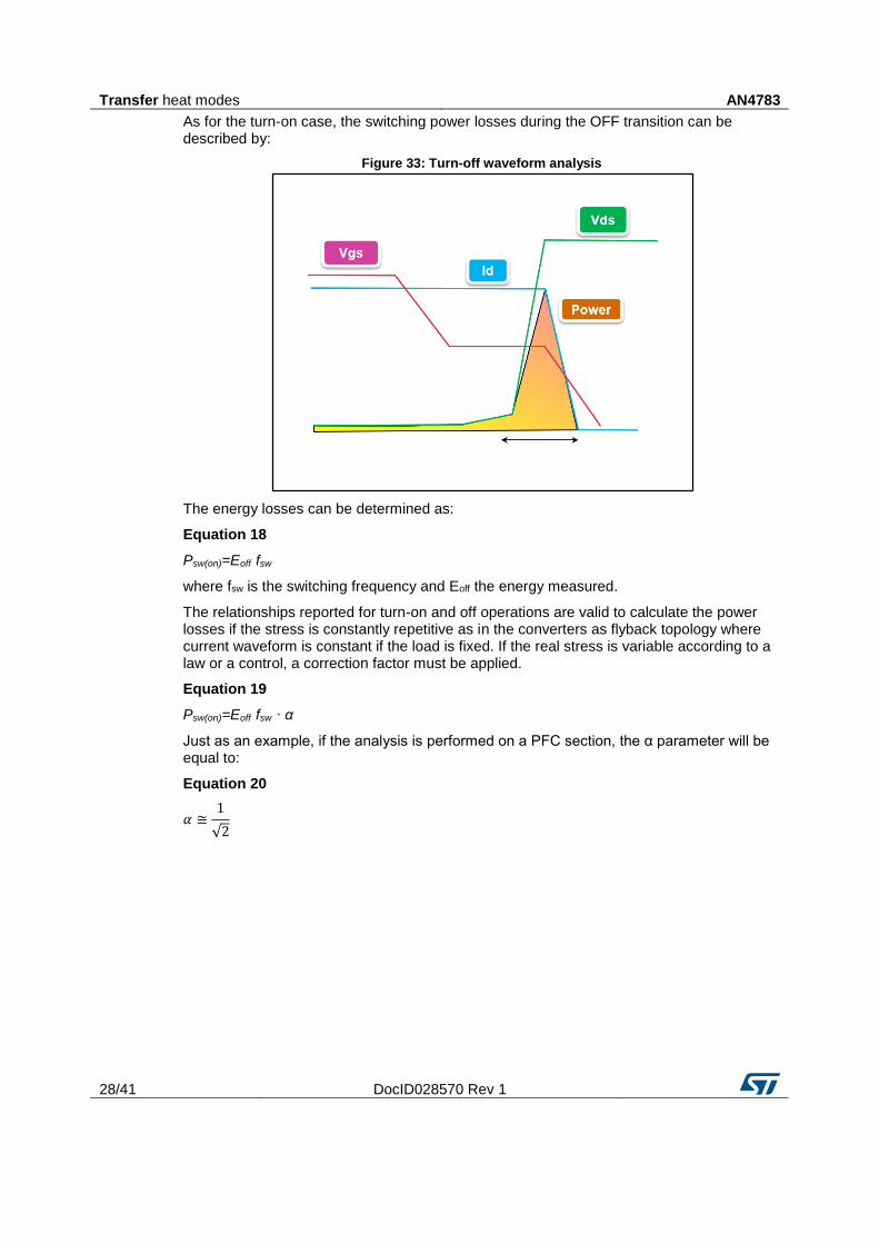
As for the turn-on case, the switching power losses during the OFF transition can be described by:
Figure 33: Turn-off waveform analysis
The energy losses can be determined as:
Equation 18
Psw(on)=Eoff·fsw
where fsw is the switching frequency and Eoff the energy measured.
The relationships reported for turn-on and off operations are valid to calculate the power losses if the stress is constantly repetitive as in the converters as flyback topology where current waveform is constant if the load is fixed. If the real stress is variable according to a law or a control, a correction factor must be applied.
Equation 19
Psw(on)=Eoff·fsw · α
Just as an example, if the analysis is performed on a PFC section, the α parameter will be equal to:
Equation 20
𝛼 ≅1
√2
AN4783 Transfer heat modes
DocID028570 Rev 1 29/41
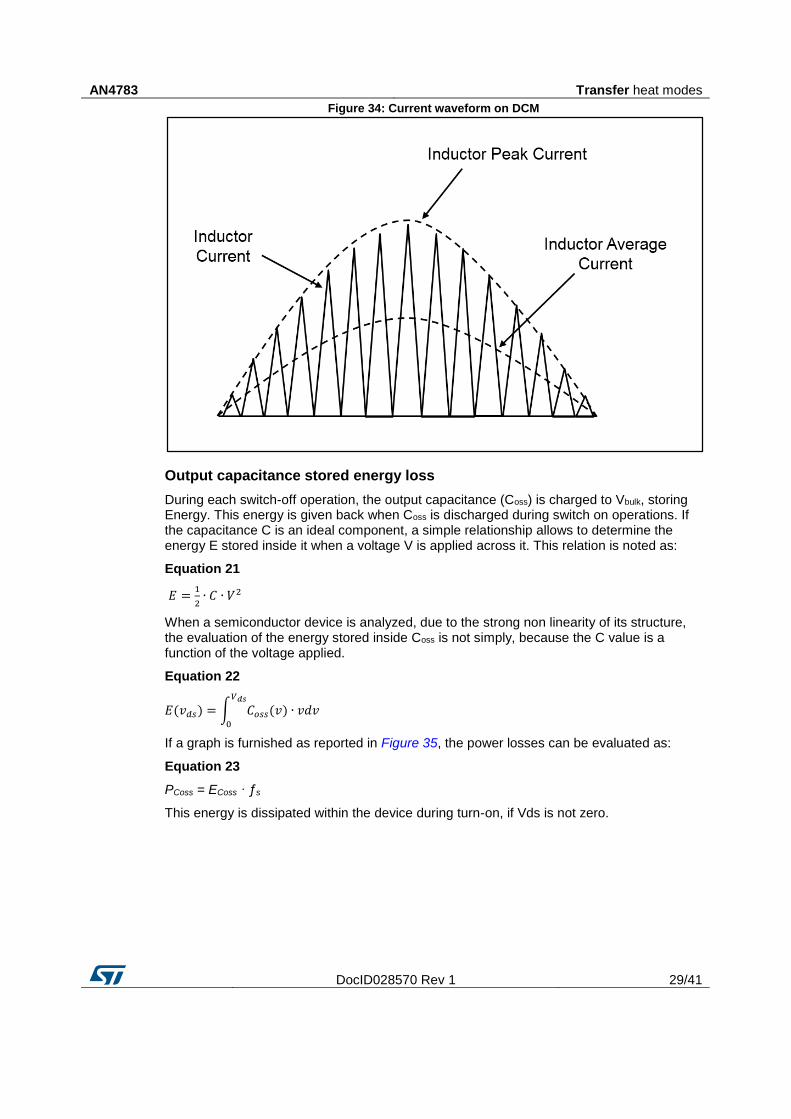
Figure 34: Current waveform on DCM
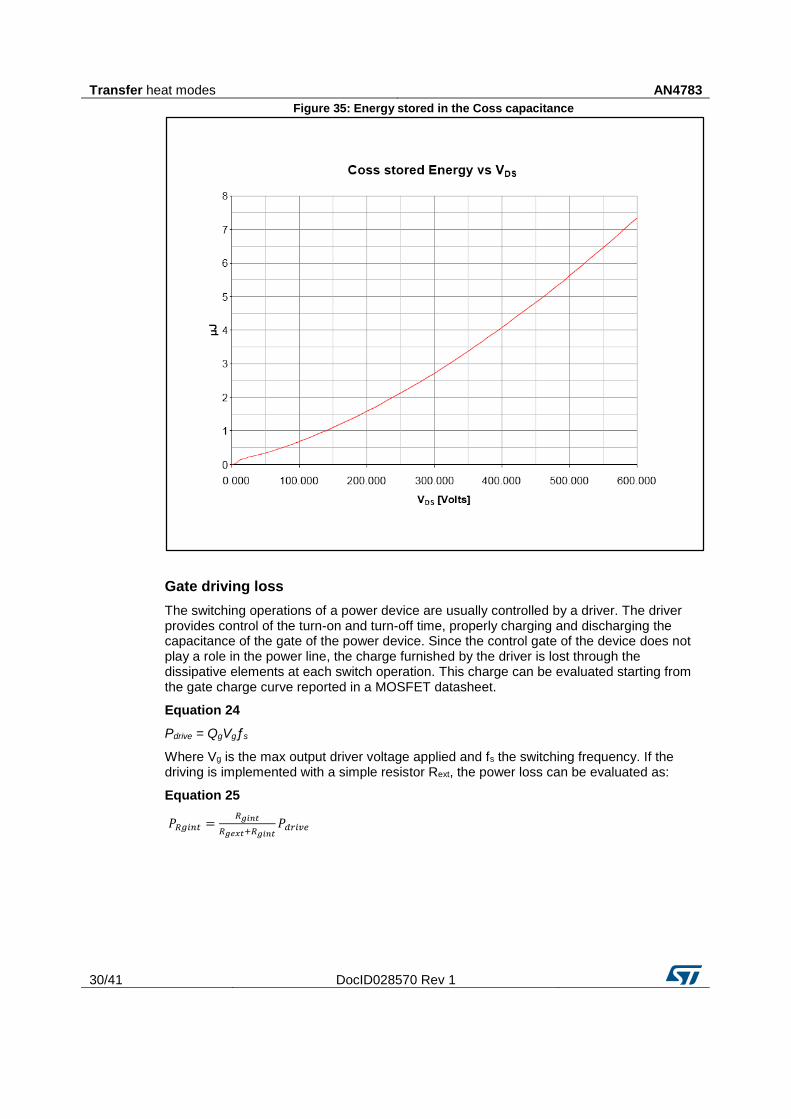
Output capacitance stored energy loss
During each switch-off operation, the output capacitance (Coss) is charged to Vbulk, storing Energy. This energy is given back when Coss is discharged during switch on operations. If the capacitance C is an ideal component, a simple relationship allows to determine the energy E stored inside it when a voltage V is applied across it. This relation is noted as:
Equation 21
𝐸 =1
2∙ 𝐶 ∙ 𝑉2
When a semiconductor device is analyzed, due to the strong non linearity of its structure, the evaluation of the energy stored inside Coss is not simply, because the C value is a function of the voltage applied.
Equation 22
𝐸(𝑣𝑑𝑠) = ∫ 𝐶𝑜𝑠𝑠(𝑣) ∙ 𝑣𝑑𝑣𝑉𝑑𝑠
0
If a graph is furnished as reported in Figure 35, the power losses can be evaluated as:
Equation 23
PCoss = ECoss · ƒs
This energy is dissipated within the device during turn-on, if Vds is not zero.
Transfer heat modes AN4783
30/41 DocID028570 Rev 1
Figure 35: Energy stored in the Coss capacitance
Gate driving loss
The switching operations of a power device are usually controlled by a driver. The driver provides control of the turn-on and turn-off time, properly charging and discharging the capacitance of the gate of the power device. Since the control gate of the device does not play a role in the power line, the charge furnished by the driver is lost through the dissipative elements at each switch operation. This charge can be evaluated starting from the gate charge curve reported in a MOSFET datasheet.
Equation 24
Pdrive = QgVgƒs
Where Vg is the max output driver voltage applied and fs the switching frequency. If the driving is implemented with a simple resistor Rext, the power loss can be evaluated as:
Equation 25
𝑃𝑅𝑔𝑖𝑛𝑡 =𝑅𝑔𝑖𝑛𝑡
𝑅𝑔𝑒𝑥𝑡+𝑅𝑔𝑖𝑛𝑡𝑃𝑑𝑟𝑖𝑣𝑒
AN4783 Example 1
DocID028570 Rev 1 31/41
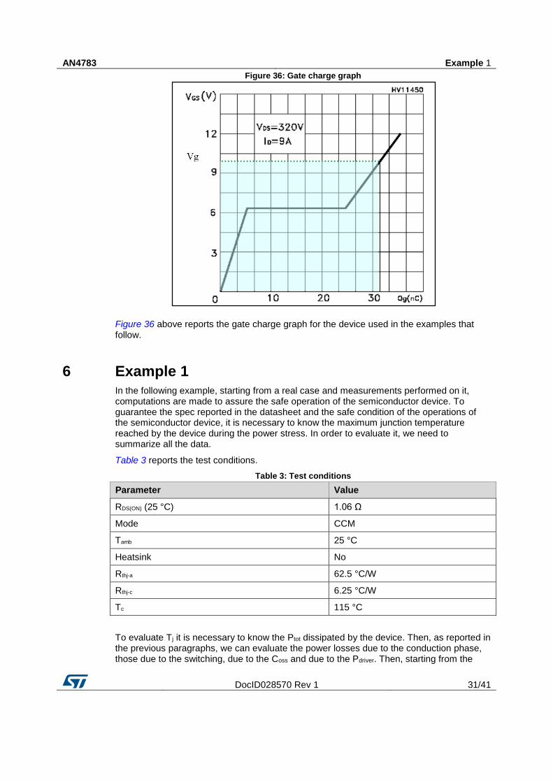
Figure 36: Gate charge graph
Figure 36 above reports the gate charge graph for the device used in the examples that follow.
6 Example 1
In the following example, starting from a real case and measurements performed on it, computations are made to assure the safe operation of the semiconductor device. To guarantee the spec reported in the datasheet and the safe condition of the operations of the semiconductor device, it is necessary to know the maximum junction temperature reached by the device during the power stress. In order to evaluate it, we need to summarize all the data.
Table 3 reports the test conditions.
Table 3: Test conditions
Parameter Value
RDS(ON) (25 °C) 1.06 Ω
Mode CCM
Tamb 25 °C
Heatsink No
Rthj-a 62.5 °C/W
Rthj-c 6.25 °C/W
Tc 115 °C
To evaluate Tj it is necessary to know the Ptot dissipated by the device. Then, as reported in the previous paragraphs, we can evaluate the power losses due to the conduction phase, those due to the switching, due to the Coss and due to the Pdriver. Then, starting from the
Example 1 AN4783
32/41 DocID028570 Rev 1
analysis of the details of the working operations, it is possible to determine the Ptot forced inside the power device.
Equation 26
Tj = Tamb + [Ptot * Rthj-a]
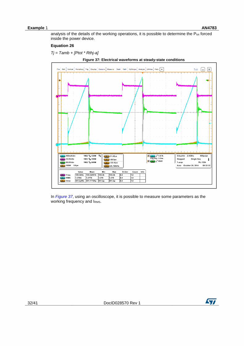
Figure 37: Electrical waveforms at steady-state conditions
In Figure 37, using an oscilloscope, it is possible to measure some parameters as the working frequency and IRMS.
AN4783 Example 1
DocID028570 Rev 1 33/41
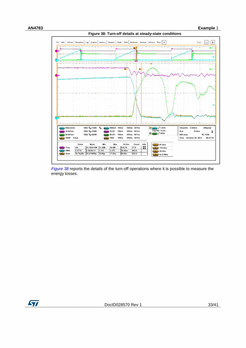
Figure 38: Turn-off details at steady-state conditions
Figure 38 reports the details of the turn-off operations where it is possible to measure the energy losses.
Example 1 AN4783
34/41 DocID028570 Rev 1
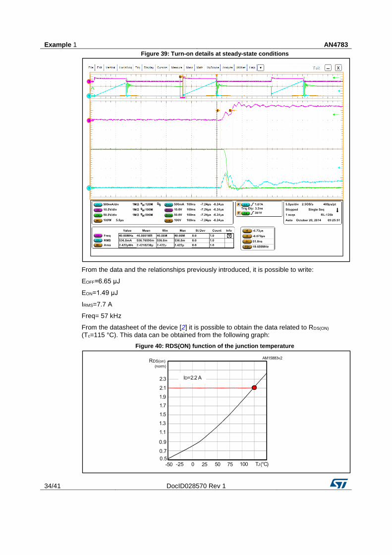
Figure 39: Turn-on details at steady-state conditions
From the data and the relationships previously introduced, it is possible to write:
EOFF=6.65 μJ
EON=1.49 μJ
IRMS=7.7 A
Freq= 57 kHz
From the datasheet of the device [2] it is possible to obtain the data related to RDS(ON) (Tc=115 °C). This data can be obtained from the following graph:
Figure 40: RDS(ON) function of the junction temperature

AN4783 Example 1
DocID028570 Rev 1 35/41
Then:
RDS(ON) (Tc=115 °C) = K RDS(ON) (Tc=25 °C) = 2.1* 1.06= 2.226 Ω
And summarizing:
Pcond= 1.15 W
Psw= 0.47 W
Pcoss= 1.47 μW
Ptot = Pcond +Psw +Pcoss = 1.62 W
Tj=Tamb + Ptot *Rthj-a = 25 +1.62 * 62.5 = 126 °C
Tc=Tj-Ptot *Rthj-c = 126-1.62 * 6.25 = 116 °C
The data estimated for the Tc is very similar to the real data as confirmed by the thermal measurement performed by thermo camera.
Figure 41: Thermal measurement during steady-state
The small difference between the data measured and the data estimated is due to the real value of some parameters reported in the datasheet such as RDS(ON), Rthj-a, Rthj-c.
Example 2 AN4783
36/41 DocID028570 Rev 1
7 Example 2
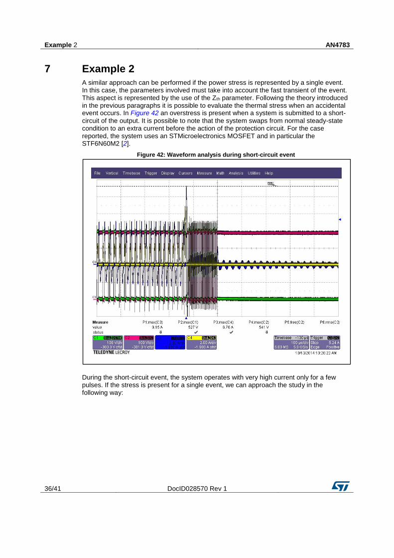
A similar approach can be performed if the power stress is represented by a single event. In this case, the parameters involved must take into account the fast transient of the event. This aspect is represented by the use of the Zth parameter. Following the theory introduced in the previous paragraphs it is possible to evaluate the thermal stress when an accidental event occurs. In Figure 42 an overstress is present when a system is submitted to a short-circuit of the output. It is possible to note that the system swaps from normal steady-state condition to an extra current before the action of the protection circuit. For the case reported, the system uses an STMicroelectronics MOSFET and in particular the STF6N60M2 [2].
Figure 42: Waveform analysis during short-circuit event
During the short-circuit event, the system operates with very high current only for a few pulses. If the stress is present for a single event, we can approach the study in the following way:
AN4783 Example 2
DocID028570 Rev 1 37/41
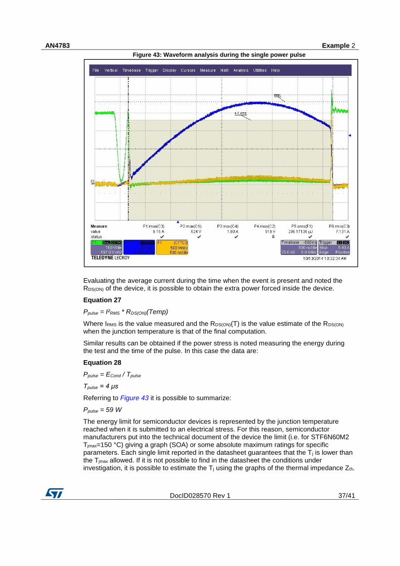
Figure 43: Waveform analysis during the single power pulse
Evaluating the average current during the time when the event is present and noted the RDS(ON) of the device, it is possible to obtain the extra power forced inside the device.
Equation 27
Ppulse = I²RMS * RDS(ON)(Temp)
Where IRMS is the value measured and the RDS(ON)(T) is the value estimate of the RDS(ON) when the junction temperature is that of the final computation.
Similar results can be obtained if the power stress is noted measuring the energy during the test and the time of the pulse. In this case the data are:
Equation 28
Ppulse = ECond / Tpulse
Tpulse = 4 μs
Referring to Figure 43 it is possible to summarize:
Ppulse = 59 W
The energy limit for semiconductor devices is represented by the junction temperature reached when it is submitted to an electrical stress. For this reason, semiconductor manufacturers put into the technical document of the device the limit (i.e. for STF6N60M2 Tjmax=150 °C) giving a graph (SOA) or some absolute maximum ratings for specific parameters. Each single limit reported in the datasheet guarantees that the T j is lower than the Tjmax allowed. If it is not possible to find in the datasheet the conditions under investigation, it is possible to estimate the Tj using the graphs of the thermal impedance Zth.

Example 2 AN4783
38/41 DocID028570 Rev 1
We need to evaluate the derating factor K and apply the formula (4.0). Let’s start, referring to Figure 44, and considering Tc = 38 °C:
Figure 44: Thermal impedance for STF6N60M2 in TO220FP
Taking into account the properties of the log-log Zth graph it is possible to extrapolate the K (4 μs) value:
Equation 29
K(4μs) = K(100µs)* SQRT(4*10-6/100*10-6)
Then
Zthj-c = K(4μ) *Rthj-c = 0.008*6.25 = 0.05 °C/W
Tj=Tc + Ppulse*Zthj-c = 38 + (59* 0.05) =40.95 °C
Since the Tj reached during the stress is lower than the max Tjmax (for this case 150 °C), the device will operate in a safe manner.
The same approach can be used in case of avalanche phenomenon where a power pulse is forced into the device only for a single event.

AN4783 References
DocID028570 Rev 1 39/41
8 References
1. N. Mohan, T. M. Undeland, W. P. Robbins: “Power Electronics: converters, applications, and design”, Second edition, John Wiley & Sons, New York, 1995.
2. STF6N60M2 datasheet 3. Agnone, A. ; Chimento, F. ; Musumeci, S. ; Raciti, A. ; Privitera, G.: “A New Thermal
Model for Power MOSFET Devices Accounting for the Behavior in Unclamped Inductive Switching” Power Electronics Specialists Conference, 2007. PESC 2007. IEEE

Revision history AN4783
40/41 DocID028570 Rev 1
9 Revision history Table 4: Document revision history
Date Version Changes
20-Nov-2015 1 Initial release.

AN4783
DocID028570 Rev 1 41/41
IMPORTANT NOTICE – PLEASE READ CAREFULLY
STMicroelectronics NV and its subsidiaries (“ST”) reserve the right to make changes, corrections, enhancements, modifications , and improvements to ST products and/or to this document at any time without notice. Purchasers should obtain the latest relevant information on ST products before placing orders. ST products are sold pursuant to ST’s terms and conditions of sale in place at the time of order acknowledgement.
Purchasers are solely responsible for the choice, selection, and use of ST products and ST assumes no liability for application assistance or the design of Purchasers’ products.
No license, express or implied, to any intellectual property right is granted by ST herein.
Resale of ST products with provisions different from the information set forth herein shall void any warranty granted by ST for such product.
ST and the ST logo are trademarks of ST. All other product or service names are the property of their respective owners.
Information in this document supersedes and replaces information previously supplied in any prior versions of this document.
© 2015 STMicroelectronics – All rights reserved