Embed Size (px)
Citation preview
June 2017 DocID027055 Rev 1 1/18
www.st.com
AN4607 Application note
Basics on the thyristor (SCR) structure and its application
Introduction This document deals with the silicon structure and electrical behavior of the thyristor. A list of the most common applications using this device is also given. For further information on thyristors and how to select the right part number according to the targeted application requirements, please refer to AN4608.
Contents AN4607
2/18 DocID027055 Rev 1
Contents
1 Thyristor basics ................................................................................ 3
1.1 Silicon structure and equivalent diagram .......................................... 3
1.2 Static electrical characteristics and basic operating modes .............. 4
1.3 Thyristor key benefits ........................................................................ 6
2 Main thyristor applications .............................................................. 7
2.1 Solid state-relays ............................................................................... 7
2.2 Bypass switch (for UPS) ................................................................... 8
2.3 Ground fault interrupter circuits and arc fault interrupter circuits ....... 9
2.4 Off-line inverters ................................................................................ 9
2.5 Vienna rectifier ................................................................................ 10
2.6 Motor speed control ........................................................................ 11
2.7 Inrush current limiter (ICL) and battery charger ............................... 12
2.8 Fluorescent tube starter / inductive ignition ..................................... 12
2.9 Capacitive ignition ........................................................................... 14
2.10 Light dimmer ................................................................................... 14
2.11 Motorbike voltage regulator ............................................................. 15
2.12 Crowbar function ............................................................................. 16
3 Conclusion ...................................................................................... 17
4 Revision history .............................................................................. 17
AN4607 Thyristor basics
DocID027055 Rev 1 3/18
1 Thyristor basics
1.1 Silicon structure and equivalent diagram
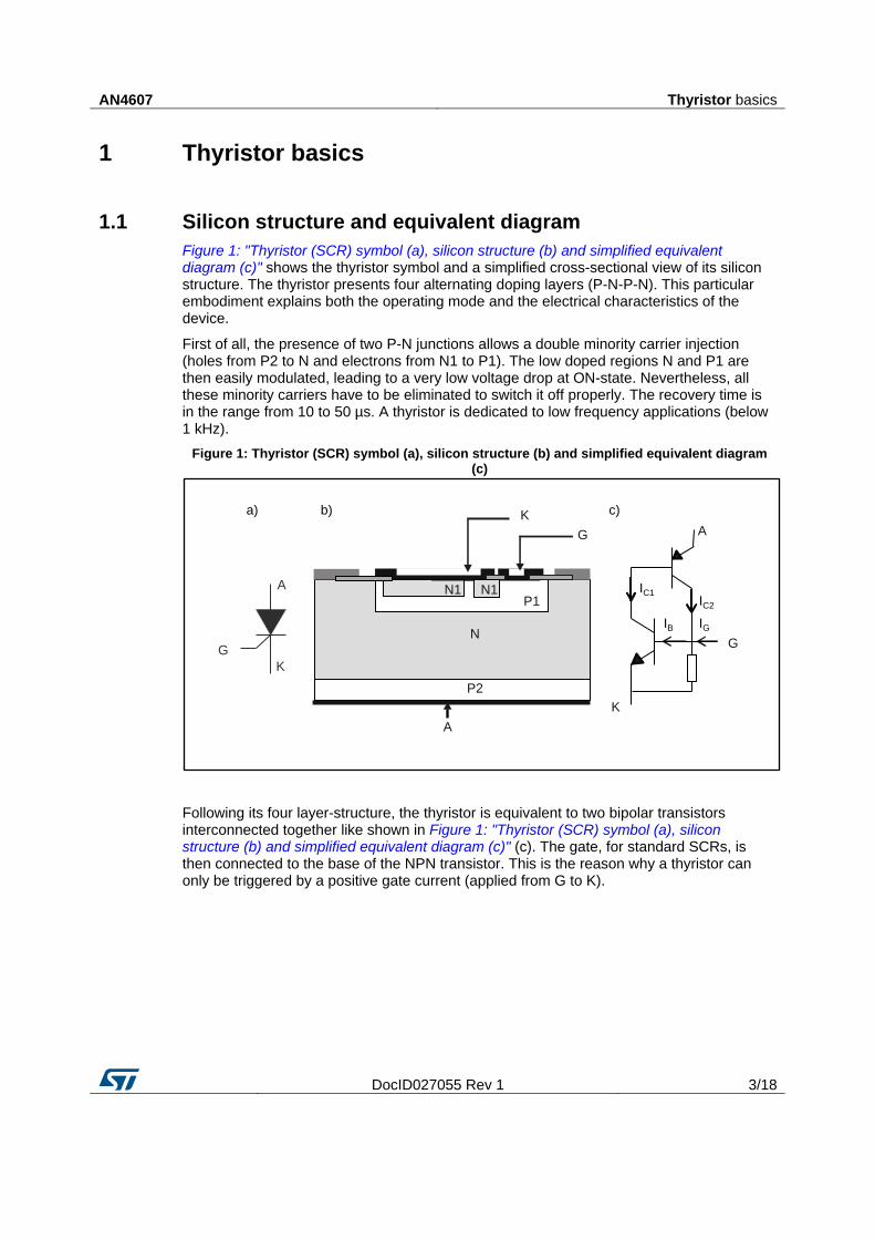
Figure 1: "Thyristor (SCR) symbol (a), silicon structure (b) and simplified equivalent diagram (c)" shows the thyristor symbol and a simplified cross-sectional view of its silicon structure. The thyristor presents four alternating doping layers (P-N-P-N). This particular embodiment explains both the operating mode and the electrical characteristics of the device.
First of all, the presence of two P-N junctions allows a double minority carrier injection (holes from P2 to N and electrons from N1 to P1). The low doped regions N and P1 are then easily modulated, leading to a very low voltage drop at ON-state. Nevertheless, all these minority carriers have to be eliminated to switch it off properly. The recovery time is in the range from 10 to 50 µs. A thyristor is dedicated to low frequency applications (below 1 kHz).
Figure 1: Thyristor (SCR) symbol (a), silicon structure (b) and simplified equivalent diagram (c)
Following its four layer-structure, the thyristor is equivalent to two bipolar transistors interconnected together like shown in Figure 1: "Thyristor (SCR) symbol (a), silicon structure (b) and simplified equivalent diagram (c)" (c). The gate, for standard SCRs, is then connected to the base of the NPN transistor. This is the reason why a thyristor can only be triggered by a positive gate current (applied from G to K).
K
G
A
P2
N
P1N1 N1A
K
G
a) b)
K
A
G
c)
IC1
IB IG
IC2
Thyristor basics AN4607
4/18 DocID027055 Rev 1
Once the NPN transistor is supplied with a base current, it draws a collector current amplified by βNPN, the NPN current gain (IC1 = βNPN.IB, refer to Figure 1: "Thyristor (SCR) symbol (a), silicon structure (b) and simplified equivalent diagram (c)" (c)). This collector current is sunk from the PNP base. The PNP base current is amplified by the PNP current gain (βPNP), leading on:
IB = βNPN x βPNP x IB + IG
This equation is valid and stable, even if the gate current is removed (IG = 0) if the following condition is ensured:
βNPN x βPNP = 1
This regeneration phenomenon makes the thyristor be latched (and the gate current can be removed) when the “βNPN x βPNP” product reaches one. The two bipolar transistor gains increase with the current, so when a sufficient gate current is applied and when a sufficient anode current circulates, the gain product reaches the unity condition leading to the regenerative operation. The gate current can then be removed and the thyristor remains latched in the on-state.
The minimum anode current needed to keep the thyristor ON is called the latching current (IL). For more information about this parameter please refer to AN303.
1.2 Static electrical characteristics and basic operating modes
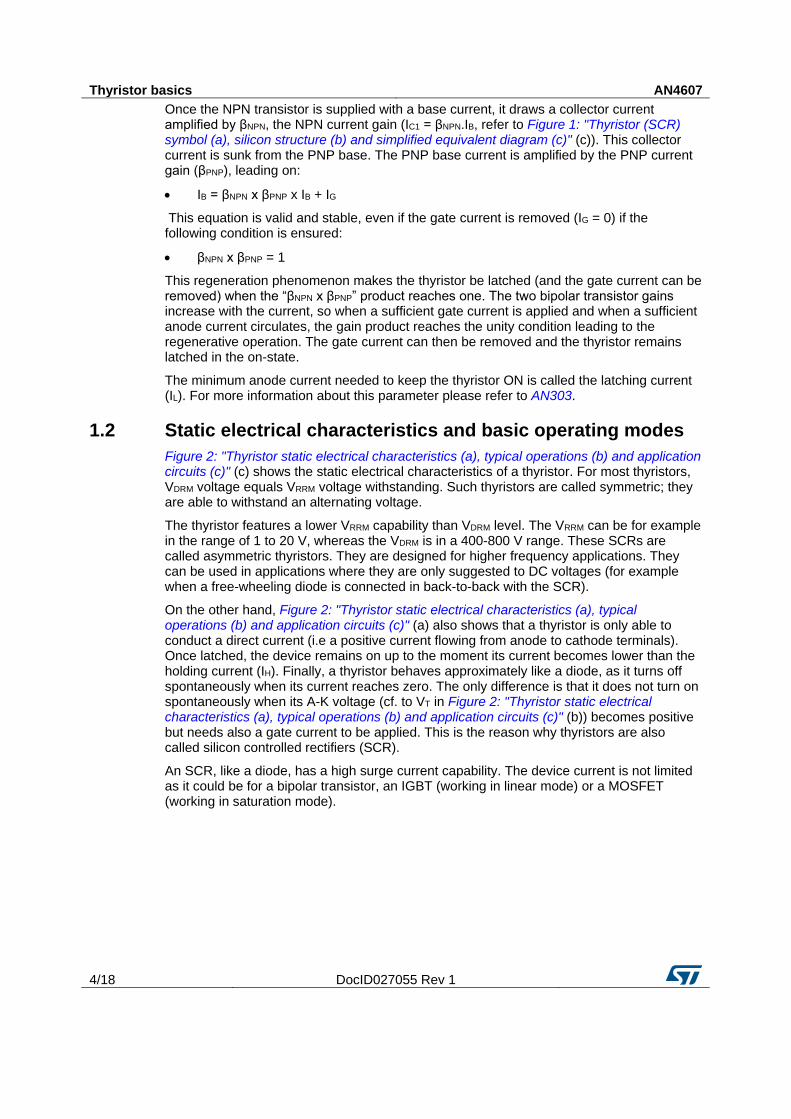
Figure 2: "Thyristor static electrical characteristics (a), typical operations (b) and application circuits (c)" (c) shows the static electrical characteristics of a thyristor. For most thyristors, VDRM voltage equals VRRM voltage withstanding. Such thyristors are called symmetric; they are able to withstand an alternating voltage.
The thyristor features a lower VRRM capability than VDRM level. The VRRM can be for example in the range of 1 to 20 V, whereas the VDRM is in a 400-800 V range. These SCRs are called asymmetric thyristors. They are designed for higher frequency applications. They can be used in applications where they are only suggested to DC voltages (for example when a free-wheeling diode is connected in back-to-back with the SCR).
On the other hand, Figure 2: "Thyristor static electrical characteristics (a), typical operations (b) and application circuits (c)" (a) also shows that a thyristor is only able to conduct a direct current (i.e a positive current flowing from anode to cathode terminals). Once latched, the device remains on up to the moment its current becomes lower than the holding current (IH). Finally, a thyristor behaves approximately like a diode, as it turns off spontaneously when its current reaches zero. The only difference is that it does not turn on spontaneously when its A-K voltage (cf. to VT in Figure 2: "Thyristor static electrical characteristics (a), typical operations (b) and application circuits (c)" (b)) becomes positive but needs also a gate current to be applied. This is the reason why thyristors are also called silicon controlled rectifiers (SCR).
An SCR, like a diode, has a high surge current capability. The device current is not limited as it could be for a bipolar transistor, an IGBT (working in linear mode) or a MOSFET (working in saturation mode).
AN4607 Thyristor basics
DocID027055 Rev 1 5/18
Figure 2: Thyristor static electrical characteristics (a), typical operations (b) and application circuits (c)
Figure 2: "Thyristor static electrical characteristics (a), typical operations (b) and application circuits (c)" (b) shows the typical operation of an SCR working in Figure 2: "Thyristor static electrical characteristics (a), typical operations (b) and application circuits (c)" schematic. The operating sequence is the following:
A positive gate current is applied when A-K voltage (VT) is positive, the SCR turns on.
The gate current pulse is removed after the SCR current has become higher than the latching current (IL). The SCR remains ON.
When the current reaches zero, the SCR turns off. It should be noted that an SCR turn-off, for a current lower than the holding current, can only be seen for low load RMS currents (below approximately 1 A). For high currents, the presence of numerous excess carriers allows the SCR to conduct up to zero without break on the current shape.
When the SCR turns off, the line voltage is reapplied across the device. If the load is inductive (like in our example), the peak line voltage is suddenly applied back to the SCR due to the current phase-lag behind the voltage.
t
t
VLINE
VT
IT
IG
t
1
2
~VLINE
Load
CTRL
VT
IT
IG
a) b) c)
IL
Switching ONif positive gatepulse currentapplied
VT
IT
Switching OFFnaturally whenIT reaches zero
12
IH
VDRM
VRRM
VBO
VBR
A
K

Thyristor basics AN4607
6/18 DocID027055 Rev 1
1.3 Thyristor key benefits
As seen in Section 1.1: "Silicon structure and equivalent diagram" and Section 1.2: "Static electrical characteristics and basic operating modes", a thyristor presents several key benefits which make it particularly interesting and useful in many applications. These benefits are:
Symmetric voltage withstanding, which allows an SCR to work in an AC voltage application without adding a diode in series.
A high overcurrent capability so that a high load current has to be withstood (such as capacitor discharge circuits; overvoltage protection crowbar circuits, motor controls).
A control by a gate current which allows a simple triggering circuit to be implemented without a complex voltage supply. Such feature is for example used in circuits where no voltage supply is available (like solid state-relays for example).
The capability to remain latched in the on-state even after the gate control signal has been removed. Such a feature is particularly useful in some protections or safety circuits (such as light alarms).
Zero-current spontaneous turn-off, which is particularly important for all ZCS switching applications (phase-control dimmer; inverter).
Overvoltage capability. Even if it is not advised to let an SCR work in breakdown area, it should be noted that when a positive voltage, higher than the VDRM, is applied to the SCR, its current begins rising once the voltage reaches the breakdown level. Then, contrary to transistors, when current increases, the device can turn on in breakover mode (when VBO voltage is reached, Figure 2: "Thyristor static electrical characteristics (a), typical operations (b) and application circuits (c)"); the energy applied to the SCR in the breakdown area is so limited as the SCR turns on and does not work in clamping mode for a long time. Even if a device is not necessarily damaged after a breakover, it should not occur in the device applications in a repetitive way, unless this operating mode is guaranteed for a specific thyristor part number (within specific conditions given in the device datasheet). It should also be noted that any SCR is not able to turn on in breakover mode for reverse voltages. For negative bias, the overvoltage protection is then mandatory even for those devices guaranteed in breakover mode if the maximum voltage applied to the application exceeds the VRRM or VRSM level. Refer to AN4608 for overvoltage protection circuit examples.
AN4607 Main thyristor applications
DocID027055 Rev 1 7/18
2 Main thyristor applications
2.1 Solid state-relays
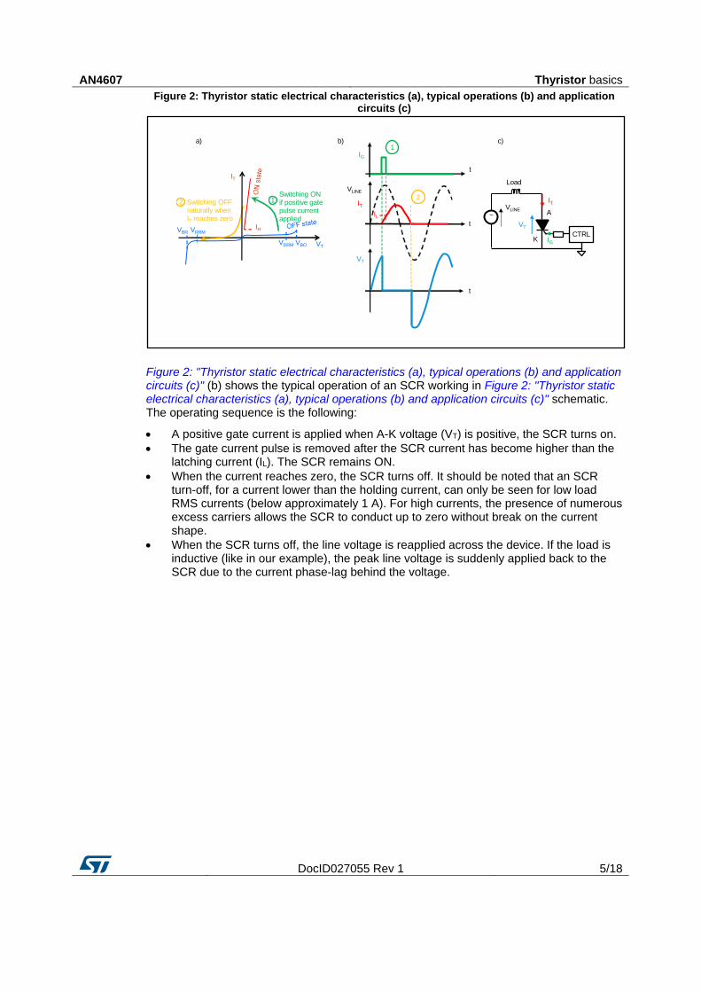
SCRs are mainly used in high power industrial applications such as solid state-relays (SSR). An SSR relay usually features two SCRs in back-to-back (Q1 and Q2 on Figure 2: "Thyristor static electrical characteristics (a), typical operations (b) and application circuits (c)") to achieve an alternative current (AC) switch. Two SCRs are preferred instead of a single triac to allow the SSR to control a higher current. Triacs are indeed limited to current ranges up to 30-40 A especially due to the turn-off (dI/dt) limitation (refer to AN4363).
The key parameters for an SCR in these applications are:
VDRM / VRRM : usually 800 V devices are used for single-phase applications and 1000-1200 V devices for three-phase. A high voltage withstanding is requested as an SSR can control a motor which could apply back a supplementary voltage to the SCR due to the motor back-electromotive force.
IT(RMS) : SSRs are usually high power applications with a load current above 6 A. 8 A to 80 A devices are often used depending on the SSR current ratings.
IGT: devices with IGT higher than 30 mA are preferred as they feature a better dV/dt immunity. Furthermore, as the gate current is usually provided by the grid, through the opto-triac (Figure 2: "Thyristor static electrical characteristics (a), typical operations (b) and application circuits (c)"), a high current could be applied without requiring to oversize the control circuit power supply.
The TYNxx12, the TYNxx25, the BTW69, TN3050H or the TN5050H can be used for Q1 and Q2.
Figure 3: Solid state-relay implemented with two SCRs
Figure 2: "Thyristor static electrical characteristics (a), typical operations (b) and application circuits (c)" also shows some tips to implement an SSR application:
A single opto-triac is used to control both thyristors. When the opto-triac is triggered, it applies a positive gate current to Q1 or Q2 when the line voltage is respectively positive or negative.
Diode D2 is used to give a path to Q2 gate current when the opto-triac is turned on, by keeping the reverse G-K voltage of Q1 SCR below the maximum level, which is specified (refer to parameter VRGM and AN4608). D1 diode plays the same role as D2 but when Q1 has to be triggered.
R2 and R4 resistors are used to improve the SCR immunity and to derivate the capacitive current coming from the opto-triac internal capacitor each time a transient voltage is applied to the SSR. These resistors are optional (see AN4608).
Q1
Zerocrossing
Control�circuit
P6KE400CA
Transil
LoadR1
R3
C1
R2
R4
R5
D2
D1
Opto-Triac
Q2Line
Main thyristor applications AN4607
8/18 DocID027055 Rev 1
A single transil connected between the two SCR gates allows both SCRs to be protected from any overvoltage by applying a gate current to each SCR if a too high voltage is applied to the SSR (see AN4608).
2.2 Bypass switch (for UPS)
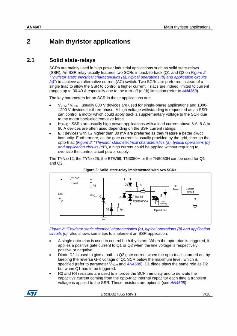
SCRs implement the bypass switch function in on-line uninterrupted power supplies (UPS). Figure 2: "Thyristor static electrical characteristics (a), typical operations (b) and application circuits (c)" gives the simplified topology of an on-line UPS. During normal operations, AC/DC rectifier provides energy both to charge the battery and to supply the input of the DC/AC inverter. This inverter continuously delivers a frequency and voltage-controlled sinus voltage to UPS load.
If UPS fails to operate, the two AC switches, implemented by the SCR couples T1-T2 and T3-T4, are turned on. Using solid-state technologies instead of mechanical switches allows the mains voltage to be applied almost instantaneously. Indeed an SCR turns on typically in one microsecond, whereas a high-power mechanical switch can have a 10 to 30 ms turn-on delay.
The two relays R1 and R2, connected in series with SCRs, are used for safety reasons. Indeed, if the line voltage collapses, the voltage is still applied to the UPS output by the inverter, which is supplied by the battery pack. But it is forbidden to inject a voltage back to the mains as an electrician may operate on the grid for maintenance purposes. This is the reason why R1 and R2 relays are used: they are switched off if the line voltage interruption is too long, in order to insulate electrically the UPS output from the inactive line.
Figure 4: Bypass switches in on-line UPS
Control topologies like those shown in Figure 2: "Thyristor static electrical characteristics (a), typical operations (b) and application circuits (c)" for SSR could be implemented here also to control the two bypass switches.
The key parameters for an SCR are identical to those of the SSR application (VDRM / VRRM : from 800 V to 1000-1200 V; IT(RMS) from 8 A to 80 A; IGT higher than 30 mA for a better dV/dt immunity). The TYNxx12, TYNxx25, BTW69, TN3050H or the TN5050H can be used because they could be high current SCRs.
Regarding to UPS AC/DC rectifier, a Vienna topology can be implemented. Please refer to Section 2.5: "Vienna rectifier" for further information.
+
+
DC
A
+
DC
Battery
AC
D
DC
DC
DC
DC
AC
AC
T1
T2T3
T4
R1
R2
UPS
outputVLINE
AN4607 Main thyristor applications
DocID027055 Rev 1 9/18
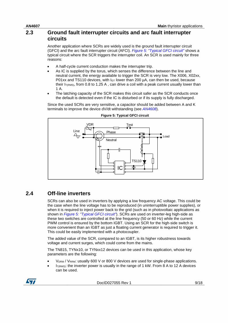
2.3 Ground fault interrupter circuits and arc fault interrupter circuits
Another application where SCRs are widely used is the ground fault interrupter circuit (GFCI) and the arc fault interrupter circuit (AFCI). Figure 5: "Typical GFCI circuit" shows a typical circuit where the SCR triggers the interrupter coil. An SCR is used mainly for three reasons:
A half-cycle current conduction makes the interrupter trip.
As IC is supplied by the torus, which senses the difference between the line and neutral current, the energy available to trigger the SCR is very low. The X006, X02xx, P01xx and TS110 devices, with IGT lower than 200 µA, can then be used, because their IT(RMS), from 0.8 to 1.25 A , can drive a coil with a peak current usually lower than 1 A.
The latching capacity of the SCR makes this circuit safer as the SCR conducts once the default is detected even if the IC is disturbed or if its supply is fully discharged.
Since the used SCRs are very sensitive, a capacitor should be added between A and K terminals to improve the device dV/dt withstanding (see AN4608).
Figure 5: Typical GFCI circuit
2.4 Off-line inverters
SCRs can also be used in inverters by applying a low frequency AC voltage. This could be the case when the line voltage has to be reproduced (in uninterruptible power supplies), or when it is required to inject power back to the grid (such as in photovoltaic applications as shown in Figure 5: "Typical GFCI circuit"). SCRs are used on inverter-leg high-side as these two switches are controlled at the line frequency (50 or 60 Hz) while the current PWM control is ensured by the bottom IGBT. Using an SCR for the high-side switch is more convenient than an IGBT as just a floating current generator is required to trigger it. This could be easily implemented with a photocoupler.
The added value of the SCR, compared to an IGBT, is its higher robustness towards voltage and current surges, which could come from the mains.
The TN815, TYNx10, or TYNxx12 devices can be used in this application, whose key parameters are the following:
VDRM / VRRM: usually 600 V or 800 V devices are used for single-phase applications.
IT(RMS): the inverter power is usually in the range of 1 kW. From 8 A to 12 A devices can be used.
IC
Phase
Neutral
Test
Load
VDR
Line
TS110
Main thyristor applications AN4607
10/18 DocID027055 Rev 1
IGT: devices with a 15 mA IGT are usually selected as they feature a better dV/dt immunity and this level of gate current can easily be provided by an opto-transistor.
Figure 6: Photovoltaic inverter (or “solar” inverter)
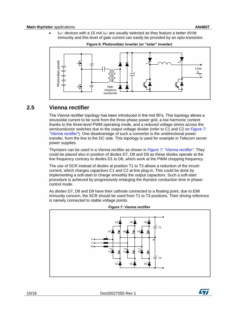
2.5 Vienna rectifier
The Vienna rectifier topology has been introduced in the mid 90’s. This topology allows a sinusoidal current to be sunk from the three-phase power grid, a low harmonic content thanks to the three-level PWM operating mode, and a reduced voltage stress across the semiconductor switches due to the output voltage divider (refer to C1 and C2 on Figure 7: "Vienna rectifier"). One disadvantage of such a converter is the unidirectional power transfer, from the line to the DC side. This topology is used for example in Telecom server power supplies.
Thyristors can be used in a Vienna rectifier as shown in Figure 7: "Vienna rectifier". They could be placed also in position of diodes D7, D8 and D9 as these diodes operate at the line frequency contrary to diodes D1 to D6, which work at the PWM chopping frequency.
The use of SCR instead of diodes at position T1 to T3 allows a reduction of the inrush current, which charges capacitors C1 and C2 at line plug-in. This could be done by implementing a soft-start to charge smoothly the output capacitors. Such a soft-start procedure is achieved by progressively enlarging the thyristor conduction time in phase-control mode.
As diodes D7, D8 and D9 have their cathode connected to a floating point, due to EMI immunity concern, the SCR should be used from T1 to T3 positions. Their driving reference is namely connected to stable voltage points.
Figure 7: Vienna rectifier
High-frequency
transformer
+
Photo
voltaic
panels
Line
+
+
C1
C2
D2D1 D3
D5D4 D6
D7 D8 D9
T1 T2 T3
M
V
U
W
L

AN4607 Main thyristor applications
DocID027055 Rev 1 11/18
The key parameters for an SCR in such an application are: a VDRM / VRRM from 800 V to 1000-1200 V; an IT(RMS) from 8 A to 80 A; an IGT higher than 15 mA for a better dV/dt immunity.
The TN815, TYNx10, TYNxx12, TYNxx25, BTW69, TN3050H or the TN5050H devices can be used for this application.
2.6 Motor speed control
Since the early 70’s, the thyristor was used for motor speed control. A simple analog circuit can indeed be implemented for such applications without requiring any microcontroller (see Figure 7: "Vienna rectifier"). This control can be easily achieved by an SCR or a Triac (for full AC current control) as these devices can be triggered by a current generator and do not need a stable voltage control.
Figure 7: "Vienna rectifier" also shows the circuit waveforms. The voltage applied to the motor varies according to the SCR turn-on delay (td). If td equals half-a-cycle (180° turn-on angle), no voltage is applied to the motor and it remains off. When td equals zero, the whole line half-cycle is applied to the motor, which runs to the highest controlled speed.
This speed-control method, by varying the voltage applied to the motor, works mainly with universal motors (for tools or kitchen blender applications). Some asynchronous AC induction motors can also work with a control circuit (when a Triac is used) but only if a low mechanical torque is present at low speed (such as fan applications).
The motor is here only supplied by a positive current. Such half-cycle control can only be accepted for low-power loads so not to sink a too high DC current on the mains (to avoid grid voltage transformer saturation).
The X04, TS420 or TS820 devices can be used for this applicatiopn, whose key parameters are the following:
IT(RMS): as the load power is usually lower than 500 W, from 4 A to 8 A devices can be used.
IGT: sensitive devices with an IGT lower than 0.2 mA are used if an analog control is implemented like shown in Figure 7: "Vienna rectifier". When the control circuit can deliver a higher current, 10 to 35 mA IGT devices can be used to reach a higher dV/dt immunity and avoid adding an RC snubber circuit in parallel to the SCR.
Figure 8: Universal motor speed-control and associated waveforms
M
P
VT
IT
ttd
VLINE
VT
IT
VLINE
Main thyristor applications AN4607
12/18 DocID027055 Rev 1
2.7 Inrush current limiter (ICL) and battery charger
SCRs are also used to bypass the inrush-current limiter resistor (refer to RLIM on Figure 9: "Inrush-current limiter resistor bypass with the SCR (a: DC side; b: bridge side)"), which is present in most applications featuring a rectifier bridge. Refer to AN4606 for more information on this application.
The TN815, TYNx10, TYNxx12, BTW69, TN3050H or TN5050H-12WY (automotive grade SCR for on-board battery chargers) devices can be used for this application, whose key parameters to select the right SCRs are:
VDRM / VRRM: usually 800 V and 1000-1200 V devices are respectively used for single-phase and three-phase applications.
IT(RMS): these applications are usually high-power applications with load current above 6 A, thus 8 A to 80 A devices are required.
IGT: devices with IGT higher than 15 mA are preferred as they feature a better dV/dt immunity.
Figure 9: Inrush-current limiter resistor bypass with the SCR (a: DC side; b: bridge side)
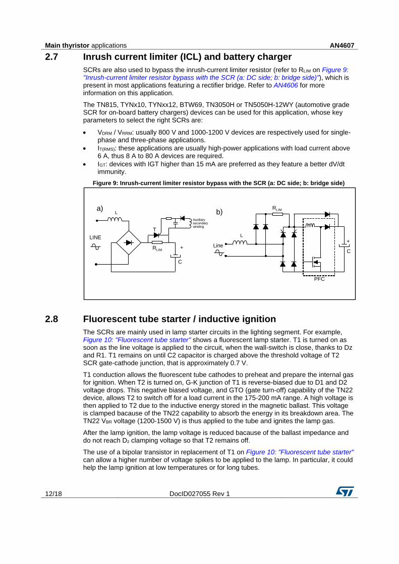
2.8 Fluorescent tube starter / inductive ignition
The SCRs are mainly used in lamp starter circuits in the lighting segment. For example, Figure 10: "Fluorescent tube starter" shows a fluorescent lamp starter. T1 is turned on as soon as the line voltage is applied to the circuit, when the wall-switch is close, thanks to Dz and R1. T1 remains on until C2 capacitor is charged above the threshold voltage of T2 SCR gate-cathode junction, that is approximately 0.7 V.
T1 conduction allows the fluorescent tube cathodes to preheat and prepare the internal gas for ignition. When T2 is turned on, G-K junction of T1 is reverse-biased due to D1 and D2 voltage drops. This negative biased voltage, and GTO (gate turn-off) capability of the TN22 device, allows T2 to switch off for a load current in the 175-200 mA range. A high voltage is then applied to T2 due to the inductive energy stored in the magnetic ballast. This voltage is clamped bacause of the TN22 capability to absorb the energy in its breakdown area. The TN22 VBR voltage (1200-1500 V) is thus applied to the tube and ignites the lamp gas.
After the lamp ignition, the lamp voltage is reduced bacause of the ballast impedance and do not reach Dz clamping voltage so that T2 remains off.
The use of a bipolar transistor in replacement of T1 on Figure 10: "Fluorescent tube starter" can allow a higher number of voltage spikes to be applied to the lamp. In particular, it could help the lamp ignition at low temperatures or for long tubes.
a)b)
+
C
L
RLIM
+RLIM
Auxiliarysecondarywinding
T
C
L
LINE
Line
PFC

AN4607 Main thyristor applications
DocID027055 Rev 1 13/18
Figure 10: Fluorescent tube starter
STARTER
TUBE
LAMP
BALLAST
T1
TN22-1500H
T2
P0102
VLINE
R1
R3
R2
R4C1
C2
D1
D2
Dz
SMAJ170A

Main thyristor applications AN4607
14/18 DocID027055 Rev 1
2.9 Capacitive ignition
The previous lamp starter belongs to the inductive igniter family. SCRs are mainly used in capacitive ignitions (as shown in Figure 11: "Lamp capacitive igniter with electronic ballast"). These types of ignitions are used in lamp starters (mainly for HID lamps) and can also be used for the engine ignition in motor bikes, or for flash ignition for cameras.
In Figure 11: "Lamp capacitive igniter with electronic ballast", the SCR is turned on once C3 capacitor reaches Diac VBO threshold. C2 capacitor, which was previously charged to the DC bus voltage (“HV DC” which is close to 320-340 V) through R1 resistor, is then suddenly discharged through the transformer primary, resulting in the application of a high voltage to the secondary winding, thus leading to the lamp ignition.
The X00602, X00619 or X02 devices can be used in this kind of application because they are sensitive SCRs with IT(RMS) level lower than 1.25 A.
Figure 11: Lamp capacitive igniter with electronic ballast
2.10 Light dimmer
SCRs can also be used in light dimmer applications, where they can replace a triac to suppress the flickering effect on CFL or LED lamps. Figure 11: "Lamp capacitive igniter with electronic ballast" shows a dimmer circuit. The IGBT is used just to limit the EMI content due to the current transitions, which occur every each half-cycle turn-on. The SCR ensures the current conduction with a low voltage drop, which is particularly interesting when halogen lamps in the range of 300-1000 W have to be dimmed.
The TS820 or TS1220 devices are used in this kind of application, with 200 µA IGT and 8-12 A IT(RMS). An insulated full-pack package allows both of SCRs to be mounted on a same heat sink. For more information about this circuit, please refer to the STEVAL-ILD003V1 / STEVAL-ILD003V2 and STEVAL-ILD004V1 / STEVAL-ILD004V2 evaluation boards.
Filter
HV DC
C1
LA
MP
VLINE
DiacT
IGNITER
C2
C3
R2
R1
AN4607 Main thyristor applications
DocID027055 Rev 1 15/18
Figure 12: Dimmer for halogen, CFL and LED lamps
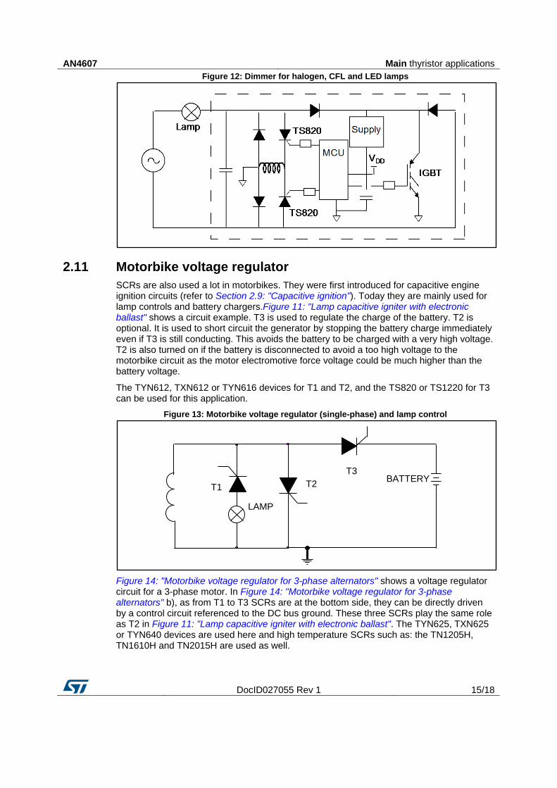
2.11 Motorbike voltage regulator
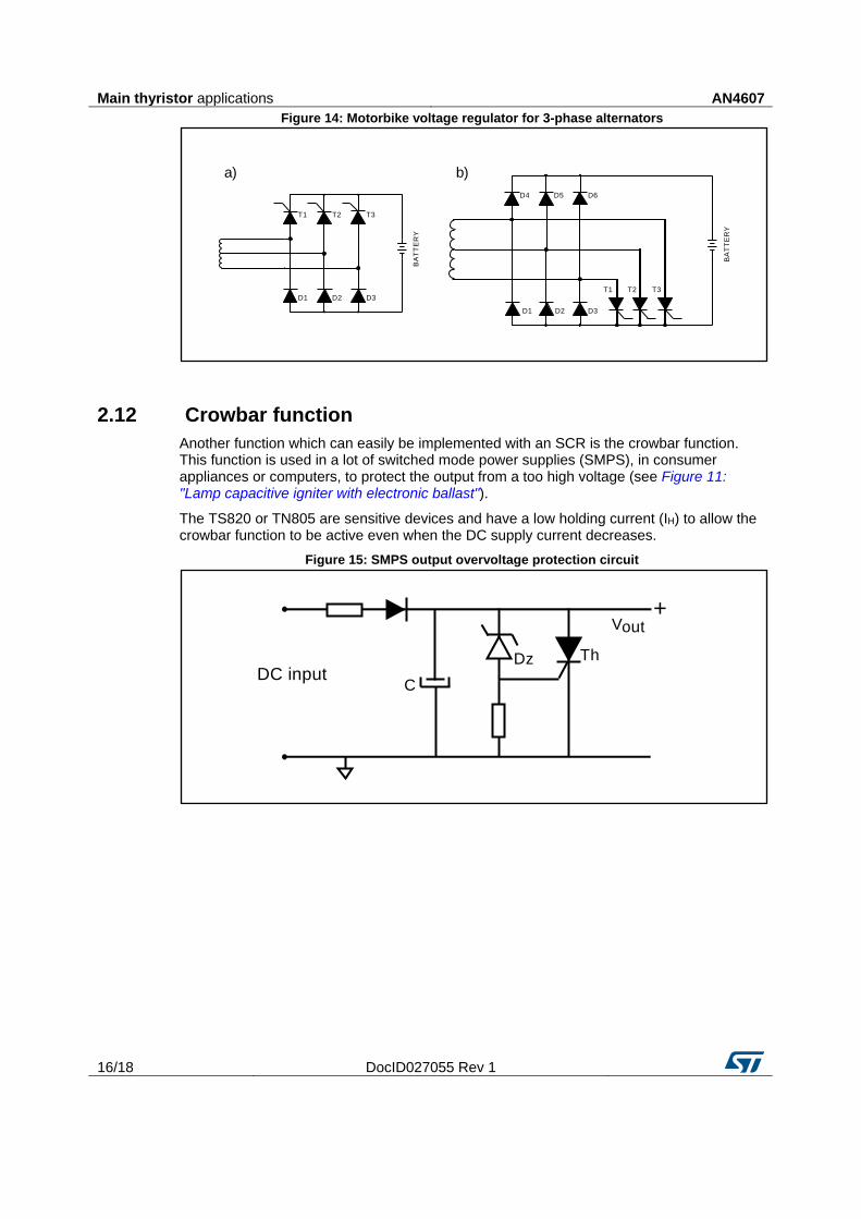
SCRs are also used a lot in motorbikes. They were first introduced for capacitive engine ignition circuits (refer to Section 2.9: "Capacitive ignition"). Today they are mainly used for lamp controls and battery chargers.Figure 11: "Lamp capacitive igniter with electronic ballast" shows a circuit example. T3 is used to regulate the charge of the battery. T2 is optional. It is used to short circuit the generator by stopping the battery charge immediately even if T3 is still conducting. This avoids the battery to be charged with a very high voltage. T2 is also turned on if the battery is disconnected to avoid a too high voltage to the motorbike circuit as the motor electromotive force voltage could be much higher than the battery voltage.
The TYN612, TXN612 or TYN616 devices for T1 and T2, and the TS820 or TS1220 for T3 can be used for this application.
Figure 13: Motorbike voltage regulator (single-phase) and lamp control
Figure 14: "Motorbike voltage regulator for 3-phase alternators" shows a voltage regulator circuit for a 3-phase motor. In Figure 14: "Motorbike voltage regulator for 3-phase alternators" b), as from T1 to T3 SCRs are at the bottom side, they can be directly driven by a control circuit referenced to the DC bus ground. These three SCRs play the same role as T2 in Figure 11: "Lamp capacitive igniter with electronic ballast". The TYN625, TXN625 or TYN640 devices are used here and high temperature SCRs such as: the TN1205H, TN1610H and TN2015H are used as well.
T2BATTERY
T3
T1
LAMP
Main thyristor applications AN4607
16/18 DocID027055 Rev 1
Figure 14: Motorbike voltage regulator for 3-phase alternators
2.12 Crowbar function
Another function which can easily be implemented with an SCR is the crowbar function. This function is used in a lot of switched mode power supplies (SMPS), in consumer appliances or computers, to protect the output from a too high voltage (see Figure 11: "Lamp capacitive igniter with electronic ballast").
The TS820 or TN805 are sensitive devices and have a low holding current (IH) to allow the crowbar function to be active even when the DC supply current decreases.
Figure 15: SMPS output overvoltage protection circuit
T1
D1 D2
T2
D3
T3
D4
BA
TT
ER
Y
D1 D2
D5
D3
D6
T1 T2 T3
BA
TT
ER
Y
a) b)
Vout+
ThDz
CDC input

AN4607 Conclusion
DocID027055 Rev 1 17/18
3 Conclusion In this application note, the silicon structure and the electrical behavior of the thyristor (or the SCR, silicon controlled rectifier) have been handled.
The SCRs are used in a wide range of applications: appliance, industrial, automotive, computer or lighting segments. They are used in functions where their latch-up capability, their easiness to be triggered by a low gate current, and their high voltage and current withstanding provide key benefits for the whole circuit performance.
Further information can be found in the following application notes:
AN302 and AN303 handle in detail the latching and holding current parameters.
AN392 gives basic information about triac control with a microcontroller (given information could be adapted to the SCR device).
AN533 lists precautions for the correct mounting and cooling of the SCR/triac devices.
AN2703 gives the definition of triac, ACST, ACS, SCR datasheet parameters.
AN4608 explains how to select the right SCR device according to application requirements.
AN4606 details the inrush-current limiter applications.
4 Revision history Table 1: Document revision history
Date Revision Changes
23-Jun-2017 1 First release

AN4607
18/18 DocID027055 Rev 1
IMPORTANT NOTICE – PLEASE READ CAREFULLY
STMicroelectronics NV and its subsidiaries (“ST”) reserve the right to make changes, corrections, enhancements, modifications, and improvements to ST products and/or to this document at any time without notice. Purchasers should obtain the latest relevant information on ST products before placing orders. ST products are sold pursuant to ST’s terms and conditions of sale in place at the time of order acknowledgement.
Purchasers are solely responsible for the choice, selection, and use of ST products and ST assumes no liability for application assistance or the design of Purchasers’ products.
No license, express or implied, to any intellectual property right is granted by ST herein.
Resale of ST products with provisions different from the information set forth herein shall void any warranty granted by ST for such product.
ST and the ST logo are trademarks of ST. All other product or service names are the property of their respective owners.
Information in this document supersedes and replaces information previously supplied in any prior versions of this document.
© 2017 STMicroelectronics – All rights reserved