Embed Size (px)
Citation preview
Freescale SemiconductorApplication Note
© 2011, 2014 Freescale Semiconductor, Inc. All rights reserved.
This design checklist provides recommendations for new designs based on the P1022 QorIQ integrated processor. The P1022 combines dual e500v2 processor cores built on Power Architecture® technology with system logic required for networking, wireless infrastructure, and telecommunications applications.
This document may also be useful in debugging newly designed systems by highlighting those aspects of a design that merit special attention during initial system start-up.
For updates to this document, see the website listed on the last page.
Document Number: AN4343Rev. 1, 05/2014
Contents
1. Simplifying the First Phase of Design . . . . . . . . . . . . 22. Power Design Considerations . . . . . . . . . . . . . . . . . . . 43. Power-on Reset and Reset Configurations . . . . . . . . . 74. Misc Debug and Test Interface Pin Recommendations .
115. Device Pins and Recommended Test Points . . . . . . . 126. Clock Pin Recommendations . . . . . . . . . . . . . . . . . . 127. DDR Interface Pin Recommendations . . . . . . . . . . . 198. DUART, IIC, and SSI Interface Pin Recommendations .
209. eSDHC Interface Pin Recommendations . . . . . . . . . 21
10. eSPI Interface Pin Recommendations . . . . . . . . . . . . 2111. USB Interface Pin Recommendations . . . . . . . . . . . 2212. Ethernet Management Interface Pin Recommendations .
2313. eTSEC Interface Pin Recommendations . . . . . . . . . . 2314. JTAG Interface Pin Recommendations . . . . . . . . . . . 2415. eLBC Interface Pin Recommendations . . . . . . . . . . . 2716. PIC Interface Pin Recommendations . . . . . . . . . . . . 3117. GPIO Interface Pin Recommendations . . . . . . . . . . . 3218. SerDes Interface Pin Recommendations . . . . . . . . . . 3219. eTSEC IEEE 1588 Pin Recommendations . . . . . . . . 3420. System Control Pin Recommendations . . . . . . . . . . 3421. Reserved POR Configuration Pins . . . . . . . . . . . . . . 3522. Power Management . . . . . . . . . . . . . . . . . . . . . . . . . 3524. No-Connect Pins . . . . . . . . . . . . . . . . . . . . . . . . . . . . 3825. Thermal Recommendations . . . . . . . . . . . . . . . . . . . 3826. Revision History . . . . . . . . . . . . . . . . . . . . . . . . . . . . 40
P1022 QorIQ Integrated ProcessorDesign Checklist
P1022 QorIQ Integrated Processor Design Checklist, Rev. 1
2 Freescale Semiconductor
Simplifying the First Phase of Design
1 Simplifying the First Phase of DesignThis section outlines recommendations to simplify the first phase of design. Before designing a system with a P1022 QorIQ integrated processor, it is recommended that the designer be familiar with the available documentation, software, models, and tools.
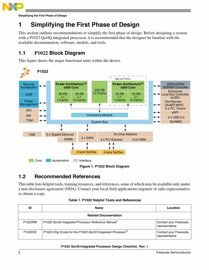
1.1 P1022 Block Diagram
This figure shows the major functional units within the device.
Figure 1. P1022 Block Diagram
1.2 Recommended References
This table lists helpful tools, training resources, and references, some of which may be available only under a non-disclosure agreement (NDA). Contact your local field applications engineer or sales representative to obtain a copy.
Table 1. P1022 Helpful Tools and References
ID Name Location
Related Documentation
P1022RM P1022 QorIQ Integrated Processor Reference Manual1 Contact your Freescale representative
P1022CE P1022 Chip Errata for the P1022 QorIQ Integrated Processor2 Contact your Freescale representative
Power Architecture™
32 KBL1
SecurityAcceleration e500 Core
256 KBL2 Cache
DDR2/DDR3SDRAM Controller
I-Cache
32 KBL1
D-Cache
Power Architecture™
32 KBL1
e500 Core
I-Cache
32 KBL1
D-Cache
Coherency Module
I-Cache
EnhancedLocal Bus Controller
(eLBC)
2 x Gigabit Ethernet
3 x PCI Express 4-ch DMA
On-Chip Network
4-lane SerDes
PowerManagement
Core Acceleration Interface
System Bus
XOR
Not on P1013
2 x SATASGMII
2-lane SerDes
1588
DIU
SSI
TDM
Perf MonitorDUART,MPIC2 x I2C, Timers
eSPI
2 x USB 2.0SD/MMC
P1022
P1022 QorIQ Integrated Processor Design Checklist, Rev. 1
Freescale Semiconductor 3
Simplifying the First Phase of Design
P1022EC P1022 QorIQ Integrated Processor Hardware Specifications Contact your Freescale representative
AN4039 PowerQUICC DDR3 SDRAM Controller Register Setting Considerations www.freescale.com
AN3369 PowerQUICC DDR2 SDRAM Controller Register Setting Considerations www.freescale.com
AN3939 DDR Interleaving for PowerQUICC and QorIQ Processors www.freescale.com
AN3659 Booting from On-Chip ROM (eSDHC or eSPI) www.freescale.com
AN2910 Hardware and Layout Design Considerations for DDR2 SDRAM Memory Interfaces www.freescale.com
AN3940 Hardware and Layout Design Considerations for DDR3 SDRAM Memory Interfaces www.freescale.com
AN3645 SEC 2/3x Descriptor Programmer’s Guide www.freescale.com
AN2919 Determining the I2C Frequency Divider Ratio for SCL www.freescale.com
AN4311 SerDes Reference Clock Interfacing and HSSI Measurements Recommendations www.freescale.com
AN2747 Power Supply Design for Power Architecture™ Processors www.freescale.com
Software Tools
I2CBOOTSEQ Boot sequencer generator tool allows configuration of any memory-mapped register before the completion of power-on reset (POR). The register data to be changed is stored in an I2C EEPROM. The P1022 requires a particular data format for register changes as outlined in the P2020RM. The boot sequencer tool (I2CBOOTSEQ) is a C-code file. When compiled and given a sample data file, it will generate the appropriate raw data format as outlined in the P1022RM. The file that is generated is an s-record file that can be used to program the EEPROM.
Contact your Freescale representative.
LBCUPMIBCG UPM Programming tool features a GUI for a user-friendly programming interface. It allows programming of all three of the P1022’s user-programmable machines. The GUI consists of a wave editor, a table editor, and a report generator. The user can edit the waveform directly or the RAM array directly. At the end of programming, the report generator will print out the UPM RAM array that can be used in a C-program.
Contact your Freescale representative.
Hardware Tools
P1022DS Development System including schematics, bill of materials, board errata list, User’s Guide, and configuration guide3
Contact your Freescale representative.
Recommended Models
IBIS To ensure first-path success, Freescale strongly recommends using the IBIS models for board-level simulations, especially for SerDes and DDR characteristics.
Contact your Freescale representative.
BSDL Use the BSDL files in board verification Contact your Freescale representative.
Flotherm Use for thermal simulation. Especially without forced cooling or constant airflow, a thermal simulation must not be skipped.
Contact your Freescale representative.
Table 1. P1022 Helpful Tools and References (continued)
ID Name Location

P1022 QorIQ Integrated Processor Design Checklist, Rev. 1
4 Freescale Semiconductor
Power Design Considerations
1.3 Product Revisions
This table lists the processor version register (PVR) and system version register (SVR) values for the various P1022 silicon derivatives.
2 Power Design ConsiderationsThis section provides design considerations for the P1022 power supplies. For information about core and I/O power consumption numbers, and thermal characteristics for the P1022, see P1022 QorIQ Integrated Processor Hardware Specifications (P1022EC).
2.1 PLL Power Supply Filtering
Each of the PLLs is provided with power through independent power supply pins (AVDD_PLAT, AVDD_COREn, AVDD_DDR, SDAVDD, and SDAVDD2, respectively). The AVDD level should always be equivalent to VDD, and these voltages must be derived directly from VDD through a low-frequency filter scheme. For the low-power mode support, AVDD_COREn should be derived from VDD and AVDD_PLAT and AVDD_DDR from VDDC.
Training
— Our third-party partners are part of an extensive Design Alliance Program. The current training partners can be found on our website under Design Alliance Program at www.freescale.com/alliances.Training material from Freescale Technology Forums are also available. These trainings modules are a valuable resource in understanding the P1022. This material is also available at our website listed on the back cover of this document
—
1 The information in the P1022RM also applies to the P1013, with the exception that the P1013 is a single-core device.2 This chip errata document describes the latest fixes and work arounds for the P1022. It is strongly recommended that the chip
errata document be thoroughly researched prior to starting a design with the P1022.3 Design requirements in the device hardware specification and design checklist supersede the design/implementation of the
P1022DS system.
Table 2. P1022 QorIQ Product Revisions
Device Number
No of Cores
Device Revision
e500 v2 CoreRevision
PVR ValuePCI
Device IDJTAG ID SVR Value TEST_SEL
P1022E 2 1.1 5.0 0x8021_1151 0x0110 068E_601D 0x80EE_0011 1
P1022 2 1.1 5.0 0x8021_1151 0x0111 068E_601D 0x80E6_0011 1
P1013E 1 1.1 5.0 0x8021_1151 0x0118 068E_701D 0x80EF_0011 0
P1013 1 1.1 5.0 0x8021_1151 0x0119 068E_701D 0x80E7_0011 0
Note: TEST_SEL must be pulled up for P1022 and pulled down for P1013.
Table 1. P1022 Helpful Tools and References (continued)
ID Name Location
P1022 QorIQ Integrated Processor Design Checklist, Rev. 1
Freescale Semiconductor 5
Power Design Considerations
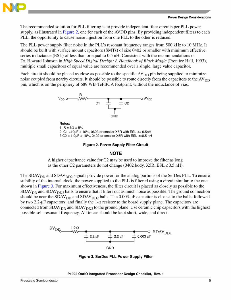
The recommended solution for PLL filtering is to provide independent filter circuits per PLL power supply, as illustrated in Figure 2, one for each of the AVDD pins. By providing independent filters to each PLL, the opportunity to cause noise injection from one PLL to the other is reduced.
The PLL power supply filter noise in the PLL’s resonant frequency ranges from 500 kHz to 10 MHz. It should be built with surface mount capacitors (SMTs) of size 0402 or smaller with minimum effective series inductance (ESL) of less than or equal to 0.5 nH. Consistent with the recommendations of Dr. Howard Johnson in High Speed Digital Design: A Handbook of Black Magic (Prentice Hall, 1993), multiple small capacitors of equal value are recommended over a single, large value capacitor.
Each circuit should be placed as close as possible to the specific AVDD pin being supplied to minimize noise coupled from nearby circuits. It should be possible to route directly from the capacitors to the AVDD pin, which is on the periphery of 689 WB-TePBGA footprint, without the inductance of vias.
Figure 2. Power Supply Filter Circuit
NOTE
A higher capacitance value for C2 may be used to improve the filter as long as the other C2 parameters do not change (0402 body, X5R, ESL 0.5 nH).
The SDAVDD and SDAVDD2 signals provide power for the analog portions of the SerDes PLL. To ensure stability of the internal clock, the power supplied to the PLL is filtered using a circuit similar to the one shown in Figure 3. For maximum effectiveness, the filter circuit is placed as closely as possible to the SDAVDD and SDAVDD2 balls to ensure that it filters out as much noise as possible. The ground connection should be near the SDAVDD and SDAVDD2 balls. The 0.003-µF capacitor is closest to the balls, followed by two 2.2-µF capacitors, and finally the 1- resistor to the board supply plane. The capacitors are connected from SDAVDD and SDAVDD2 to the ground plane. Use ceramic chip capacitors with the highest possible self-resonant frequency. All traces should be kept short, wide, and direct.
Figure 3. SerDes PLL Power Supply Filter
VDD AVDD
C1 C2
GND
R
Notes:1. R = 5± 5%2. C1 =10µF ± 10%, 0603 or smaller X5R with ESL <= 0.5nH3.C2 = 1.0µF ± 10%, 0402 or smaller X5R with ESL <=0.5 nH
2.2 µF 0.003 µF
1.0SDAVDDn
2.2 µF
GND
SVDD

P1022 QorIQ Integrated Processor Design Checklist, Rev. 1
6 Freescale Semiconductor
Power Design Considerations
NOTE
• 0805 or smaller sized SMTs recommended
• SDAVDDn should be a filtered version of SVDD
• Signals on the SerDes interface are fed from the XVDD power plane
CAUTION
These filters are a necessary extension of the PLL circuitry and are compliant with the device specifications. Any deviation from the recommended filters is done at the user’s risk.
2.2 Power Supply Decoupling Recommendations
Due to large address and data buses as well as high-operating frequencies, the device can generate transient power surges and high-frequency noise in its power supply, especially while driving large capacitive loads. To prevent the noise from reaching other components in the P1022 system, the device requires a clean, tightly regulated source of power.
The recommendations for ensuring a reliable power supply are as follows:
• Provide large power planes because immediate charge requirements by the device are always serviced from the power planes first. Refer to AN3747: Power Supply Design for PowerPC™ Processors.
• Place at least one decoupling capacitor at each VDDC,VDD, and B/G/L/OVDDn pin of the device. These decoupling capacitors should have a value of 0.1 µF and receive their power from separate VDD, VDDC, B/G/L/OVDDn, and GND planes in the PCB, utilizing short traces to minimize inductance. Capacitors may be placed directly under the device using a standard escape pattern. Others may surround the part.
• These capacitors should have a value of 0.1 µF. Only ceramic SMT capacitors should be used to minimize lead inductance, preferably 0402 or 0603 sizes.
• Several bulk storage capacitors should be distributed around the PCB, feeding the VDD, VDDC, BVDD, OVDD, OVDD2, GVDD, LVDD2, and LVDD planes, to enable quick recharging of the smaller chip capacitors.
• Bulk capacitors should be placed as close as possible to the processor. The capacitors need to be selected to work well with the power supply so as to be able to handle the P1022’s dynamic load requirements.
• These bulk capacitors should have a low ESR (equivalent series resistance) rating to ensure the quick response time necessary.
• They should also be connected to the power and ground planes through two vias to minimize inductance. Suggested bulk capacitors—100 µF to 330 µF (AVX TPS tantalum or Sanyo OSCON).
2.3 SerDes Block Power Supply Decoupling
If the SerDes module is used, it requires a clean, tightly regulated source of power (SVDD and XVDD) to ensure low jitter on transmit and reliable recovery of data in the receiver. An appropriate decoupling scheme is outlined below.
P1022 QorIQ Integrated Processor Design Checklist, Rev. 1
Freescale Semiconductor 7
Power-on Reset and Reset Configurations
• Only SMT capacitors should be used to minimize inductance. Connections from all capacitors to power and ground should be done with multiple vias to further reduce inductance.
• Board should have at least one 0.1 F SMT ceramic chip capacitors as close as possible for each supply ball of the device. If the board supports blind vias, these capacitors may be placed directly on the chip supply and ground connections. Where the board does not have blind vias, these capacitors should be placed in the central escape void, or if not possible, then in a ring around the device as close to the supply and ground connections as possible.
• There should be a 10-µF ceramic chip capacitor on the power plane of the SVDD and/or XVDD planes, on the sides of the device where those planes are present. This should be done for all SerDes supplies.
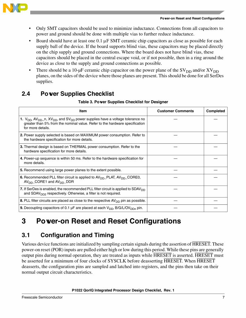
2.4 Power Supplies Checklist
3 Power-on Reset and Reset Configurations
3.1 Configuration and Timing
Various device functions are initialized by sampling certain signals during the assertion of HRESET. These power-on reset (POR) inputs are pulled either high or low during this period. While these pins are generally output pins during normal operation, they are treated as inputs while HRESET is asserted. HRESET must be asserted for a minimum of four clocks of SYSCLK before deasserting HRESET. When HRESET deasserts, the configuration pins are sampled and latched into registers, and the pins then take on their normal output circuit characteristics.
Table 3. Power Supplies Checklist for Designer
Item Customer Comments Completed
1. VDD, AVDD_n, XVDD, and SVDD power supplies have a voltage tolerance no greater than 5% from the nominal value. Refer to the hardware specification for more details.
— —
2. Power supply selected is based on MAXIMUM power consumption. Refer to the hardware specification for more details.
— —
3. Thermal design is based on THERMAL power consumption. Refer to the hardware specification for more details.
— —
4. Power-up sequence is within 50 ms. Refer to the hardware specification for more details.
— —
5. Recommend using large power planes to the extent possible. — —
6. Recommended PLL filter circuit is applied to AVDD_PLAT, AVDD_CORE0, AVDD_CORE1 and AVDD_DDR
— —
7. If SerDes is enabled, the recommended PLL filter circuit is applied to SDAVDD and SDAVDD2 respectively. Otherwise, a filter is not required.
— —
8. PLL filter circuits are placed as close to the respective AVDD pin as possible. — —
9. Decoupling capacitors of 0.1 µF are placed at each VDD, B/G/L/OVDDn pin. — —
P1022 QorIQ Integrated Processor Design Checklist, Rev. 1
8 Freescale Semiconductor
Power-on Reset and Reset Configurations
All the configuration pins have an internally gated 20 k nominal pull-up resistor, enabled only during HRESET. If default values are desired, external logic must not load or drive such pins adversely. If this cannot be guaranteed, the value must be driven actively on the pin. If default values are not desired, a 4.7 k pull-down resistor is recommended to pull the configuration pin to a valid logic low level.
An alternative to using pull-up and pull-down resistors to configure the POR pins is to use a PLD or similar device that drives the configuration signals to the P1022 when HRESET is asserted. The PLD must begin to drive these signals at least four SYSCLK cycles prior to the deassertion of HRESET (PLL configuration inputs must meet a 100 s set-up time to HRESET), hold their values for at least 5 SYSCLK cycles after the deassertion of HRESET, and then release the pins to high impedance afterward for normal device operation. For details about reset initialization timing specifications, see P1022 QorIQ Integrated Processor Hardware Specifications.
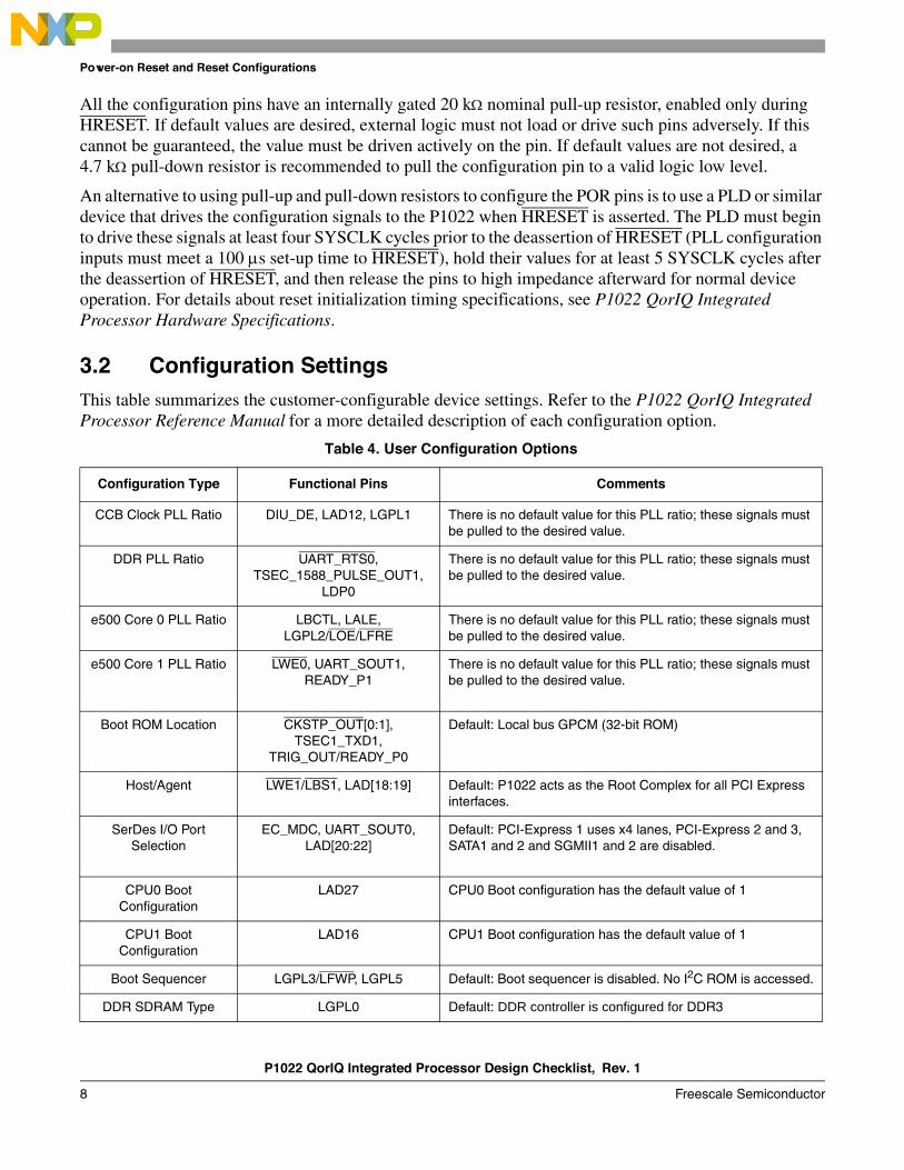
3.2 Configuration Settings
This table summarizes the customer-configurable device settings. Refer to the P1022 QorIQ Integrated Processor Reference Manual for a more detailed description of each configuration option.
Table 4. User Configuration Options
Configuration Type Functional Pins Comments
CCB Clock PLL Ratio DIU_DE, LAD12, LGPL1 There is no default value for this PLL ratio; these signals must be pulled to the desired value.
DDR PLL Ratio UART_RTS0, TSEC_1588_PULSE_OUT1,
LDP0
There is no default value for this PLL ratio; these signals must be pulled to the desired value.
e500 Core 0 PLL Ratio LBCTL, LALE, LGPL2/LOE/LFRE
There is no default value for this PLL ratio; these signals must be pulled to the desired value.
e500 Core 1 PLL Ratio LWE0, UART_SOUT1, READY_P1
There is no default value for this PLL ratio; these signals must be pulled to the desired value.
Boot ROM Location CKSTP_OUT[0:1], TSEC1_TXD1,
TRIG_OUT/READY_P0
Default: Local bus GPCM (32-bit ROM)
Host/Agent LWE1/LBS1, LAD[18:19] Default: P1022 acts as the Root Complex for all PCI Express interfaces.
SerDes I/O Port Selection
EC_MDC, UART_SOUT0, LAD[20:22]
Default: PCI-Express 1 uses x4 lanes, PCI-Express 2 and 3, SATA1 and 2 and SGMII1 and 2 are disabled.
CPU0 Boot Configuration
LAD27 CPU0 Boot configuration has the default value of 1
CPU1 Boot Configuration
LAD16 CPU1 Boot configuration has the default value of 1
Boot Sequencer LGPL3/LFWP, LGPL5 Default: Boot sequencer is disabled. No I2C ROM is accessed.
DDR SDRAM Type LGPL0 Default: DDR controller is configured for DDR3
P1022 QorIQ Integrated Processor Design Checklist, Rev. 1
Freescale Semiconductor 9
Power-on Reset and Reset Configurations
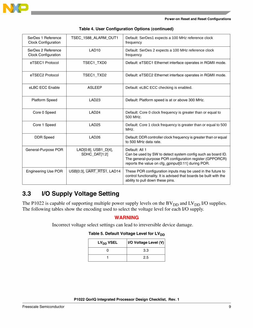
3.3 I/O Supply Voltage Setting
The P1022 is capable of supporting multiple power supply levels on the BVDD and LVDD I/O supplies. The following tables show the encoding used to select the voltage level for each I/O supply.
WARNING
Incorrect voltage select settings can lead to irreversible device damage.
SerDes 1 Reference Clock Configuration
TSEC_1588_ALARM_OUT1 Default: SerDes1 expects a 100 MHz reference clock frequency
SerDes 2 Reference Clock Configuration
LAD10 Default: SerDes 2 expects a 100 MHz reference clock frequency
eTSEC1 Protocol TSEC1_TXD0 Default: eTSEC1 Ethernet interface operates in RGMII mode.
eTSEC2 Protocol TSEC1_TXD2 Default: eTSEC2 Ethernet interface operates in RGMII mode.
eLBC ECC Enable ASLEEP Default: eLBC ECC checking is enabled.
Platform Speed LAD23 Default: Platform speed is at or above 300 MHz.
Core 0 Speed LAD24 Default: Core 0 clock frequency is greater than or equal to 500 MHz.
Core 1 Speed LAD25 Default: Core 1 clock frequency is greater than or equal to 500 MHz.
DDR Speed LAD26 Default: DDR controller clock frequency is greater than or equal to 500 MHz data rate.
General-Purpose POR LAD[0:8], USB1_D[4], SDHC_DAT[1:2]
Default: All 1Can be used by SW to detect system config such as board ID. The general-purpose POR configuration register (GPPORCR) reports the value on cfg_gpinput[0:11] during POR.
Engineering Use POR USB[0:3], UART_RTS1, LAD14 These POR configuration inputs may be used in the future to control functionality. It is advised that boards be built with the ability to pull down these pins.
Table 5. Default Voltage Level for LVDD
LVDD VSEL I/O Voltage Level (V)
0 3.3
1 2.5
Table 4. User Configuration Options (continued)

P1022 QorIQ Integrated Processor Design Checklist, Rev. 1
10 Freescale Semiconductor
Power-on Reset and Reset Configurations
NOTE
For the 8-bit eSDHC interface, BVDD should be at 3.3 V only, because the higher nibble of SDHC data pins are shared.
When the DIU functionality is used, only 3.3 V interfaces are supported on the eLBC.
Table 6. Default Voltage Level for BVDD
BVDD VSEL [0:1] I/O Voltage Level (V)
00 3.3
01 2.5
10 1.8
11 3.3
P1022 QorIQ Integrated Processor Design Checklist, Rev. 1
Freescale Semiconductor 11
Misc Debug and Test Interface Pin Recommendations
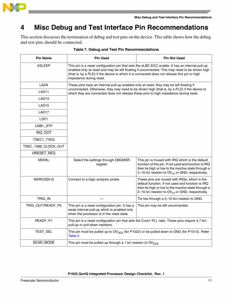
4 Misc Debug and Test Interface Pin Recommendations
This section discusses the termination of debug and test pins on the device. This table shows how the debug and test pins should be connected.
Table 7. Debug and Test Pin Recommendations
Pin Name Pin Used Pin Not Used
ASLEEP This pin is a reset configuration pin that sets the eLBC ECC enable. It has an internal pull-up enabled only at reset and may be left floating if unconnected. This may need to be driven high (that is, by a PLD) if the device to which it is connected does not release this pin to high impedance during reset.
LAD9 These pins have an internal pull-up enabled only at reset, they may be left floating if unconnected. Otherwise, they may need to be driven high (that is, by a PLD) if the device to which they are connected does not release these pins to high impedance during reset.LAD11
LAD13
LAD15
LAD17
LDP1
USB1_STP
IRQ_OUT
TSEC1_TXD3
TSEC_1588_CLOCK_OUT
HRESET_REQ
MDVAL Select the settings through DBGMSR register
This pin is muxed with IRQ which is the default function of this pin. If not used and function is IRQ then tie high or low to the inactive state through a 2–10 k resistor to OVDD or GND, respectively.
MSRCID[0:4] Connect to a logic analyzer probe. These pins are muxed with IRQs, which is the default function. If not used and function is IRQ then tie high or low to the inactive state through a 2–10 k resistor to OVDD or GND, respectively,
TRIG_IN — Tie low through a 2–10 k resistor to GND.
TRIG_OUT/READY_P0 This pin is a reset configuration pin. It has a weak internal pull-up which is enabled only when the processor is in the reset state.
This pin may be left unconnected.
READY_P1 This pin is a reset configuration pin that sets the Core1 PLL ratio. These pins require 4.7-k pull-up or pull-down resistors.
TEST_SEL This pin must be pulled up to OVDD2 (for P1022) or be pulled down to GND (for P1013). Refer Table 2
SCAN_MODE This pin must be pulled up through a 1 kresistor to OVDD2
P1022 QorIQ Integrated Processor Design Checklist, Rev. 1
12 Freescale Semiconductor
Device Pins and Recommended Test Points
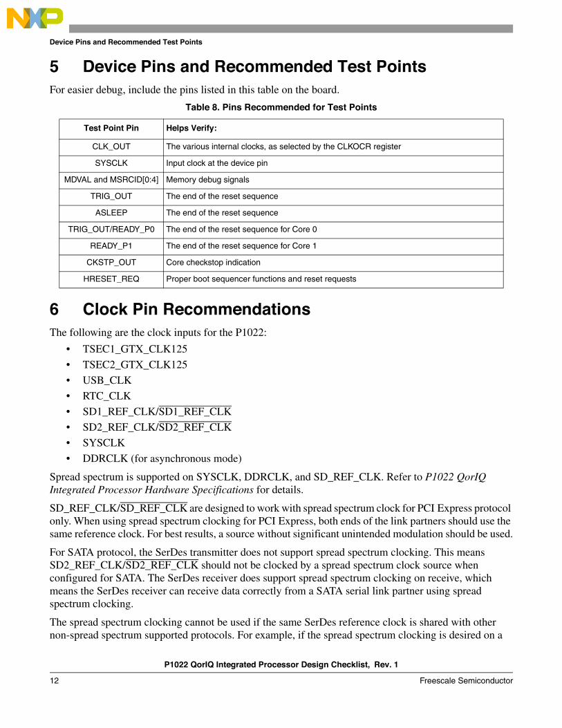
5 Device Pins and Recommended Test Points
For easier debug, include the pins listed in this table on the board.
6 Clock Pin Recommendations
The following are the clock inputs for the P1022:
• TSEC1_GTX_CLK125
• TSEC2_GTX_CLK125
• USB_CLK
• RTC_CLK
• SD1_REF_CLK/SD1_REF_CLK
• SD2_REF_CLK/SD2_REF_CLK
• SYSCLK
• DDRCLK (for asynchronous mode)
Spread spectrum is supported on SYSCLK, DDRCLK, and SD_REF_CLK. Refer to P1022 QorIQ Integrated Processor Hardware Specifications for details.
SD_REF_CLK/SD_REF_CLK are designed to work with spread spectrum clock for PCI Express protocol only. When using spread spectrum clocking for PCI Express, both ends of the link partners should use the same reference clock. For best results, a source without significant unintended modulation should be used.
For SATA protocol, the SerDes transmitter does not support spread spectrum clocking. This means SD2_REF_CLK/SD2_REF_CLK should not be clocked by a spread spectrum clock source when configured for SATA. The SerDes receiver does support spread spectrum clocking on receive, which means the SerDes receiver can receive data correctly from a SATA serial link partner using spread spectrum clocking.
The spread spectrum clocking cannot be used if the same SerDes reference clock is shared with other non-spread spectrum supported protocols. For example, if the spread spectrum clocking is desired on a
Table 8. Pins Recommended for Test Points
Test Point Pin Helps Verify:
CLK_OUT The various internal clocks, as selected by the CLKOCR register
SYSCLK Input clock at the device pin
MDVAL and MSRCID[0:4] Memory debug signals
TRIG_OUT The end of the reset sequence
ASLEEP The end of the reset sequence
TRIG_OUT/READY_P0 The end of the reset sequence for Core 0
READY_P1 The end of the reset sequence for Core 1
CKSTP_OUT Core checkstop indication
HRESET_REQ Proper boot sequencer functions and reset requests
P1022 QorIQ Integrated Processor Design Checklist, Rev. 1
Freescale Semiconductor 13
Clock Pin Recommendations
SerDes reference clock for PCI Express, and the same reference clock is used for any other protocol like SGMII due to SerDes lane usage mapping option, then spread spectrum clocking cannot be used at all.
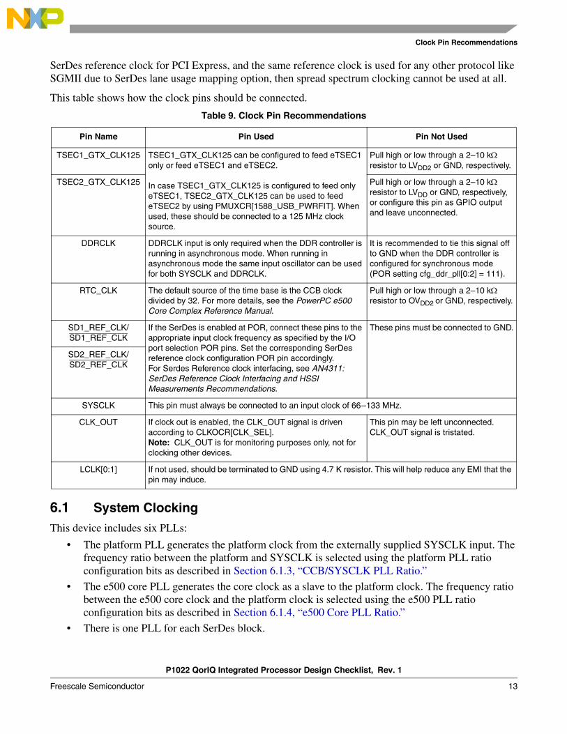
This table shows how the clock pins should be connected.
6.1 System Clocking
This device includes six PLLs:
• The platform PLL generates the platform clock from the externally supplied SYSCLK input. The frequency ratio between the platform and SYSCLK is selected using the platform PLL ratio configuration bits as described in Section 6.1.3, “CCB/SYSCLK PLL Ratio.”
• The e500 core PLL generates the core clock as a slave to the platform clock. The frequency ratio between the e500 core clock and the platform clock is selected using the e500 PLL ratio configuration bits as described in Section 6.1.4, “e500 Core PLL Ratio.”
• There is one PLL for each SerDes block.
Table 9. Clock Pin Recommendations
Pin Name Pin Used Pin Not Used
TSEC1_GTX_CLK125 TSEC1_GTX_CLK125 can be configured to feed eTSEC1 only or feed eTSEC1 and eTSEC2.
In case TSEC1_GTX_CLK125 is configured to feed only eTSEC1, TSEC2_GTX_CLK125 can be used to feed eTSEC2 by using PMUXCR[1588_USB_PWRFIT]. When used, these should be connected to a 125 MHz clock source.
Pull high or low through a 2–10 k resistor to LVDD2 or GND, respectively.
TSEC2_GTX_CLK125 Pull high or low through a 2–10 k resistor to LVDD or GND, respectively, or configure this pin as GPIO output and leave unconnected.
DDRCLK DDRCLK input is only required when the DDR controller is running in asynchronous mode. When running in asynchronous mode the same input oscillator can be used for both SYSCLK and DDRCLK.
It is recommended to tie this signal off to GND when the DDR controller is configured for synchronous mode (POR setting cfg_ddr_pll[0:2] = 111).
RTC_CLK The default source of the time base is the CCB clock divided by 32. For more details, see the PowerPC e500 Core Complex Reference Manual.
Pull high or low through a 2–10 k resistor to OVDD2 or GND, respectively.
SD1_REF_CLK/ SD1_REF_CLK
If the SerDes is enabled at POR, connect these pins to the appropriate input clock frequency as specified by the I/O port selection POR pins. Set the corresponding SerDes reference clock configuration POR pin accordingly.For Serdes Reference clock interfacing, see AN4311: SerDes Reference Clock Interfacing and HSSI Measurements Recommendations.
These pins must be connected to GND.
SD2_REF_CLK/ SD2_REF_CLK
SYSCLK This pin must always be connected to an input clock of 66–133 MHz.
CLK_OUT If clock out is enabled, the CLK_OUT signal is driven according to CLKOCR[CLK_SEL].Note: CLK_OUT is for monitoring purposes only, not for clocking other devices.
This pin may be left unconnected. CLK_OUT signal is tristated.
LCLK[0:1] If not used, should be terminated to GND using 4.7 K resistor. This will help reduce any EMI that the pin may induce.
P1022 QorIQ Integrated Processor Design Checklist, Rev. 1
14 Freescale Semiconductor
Clock Pin Recommendations
• There is one PLL for the DDR for asynchronous operation.
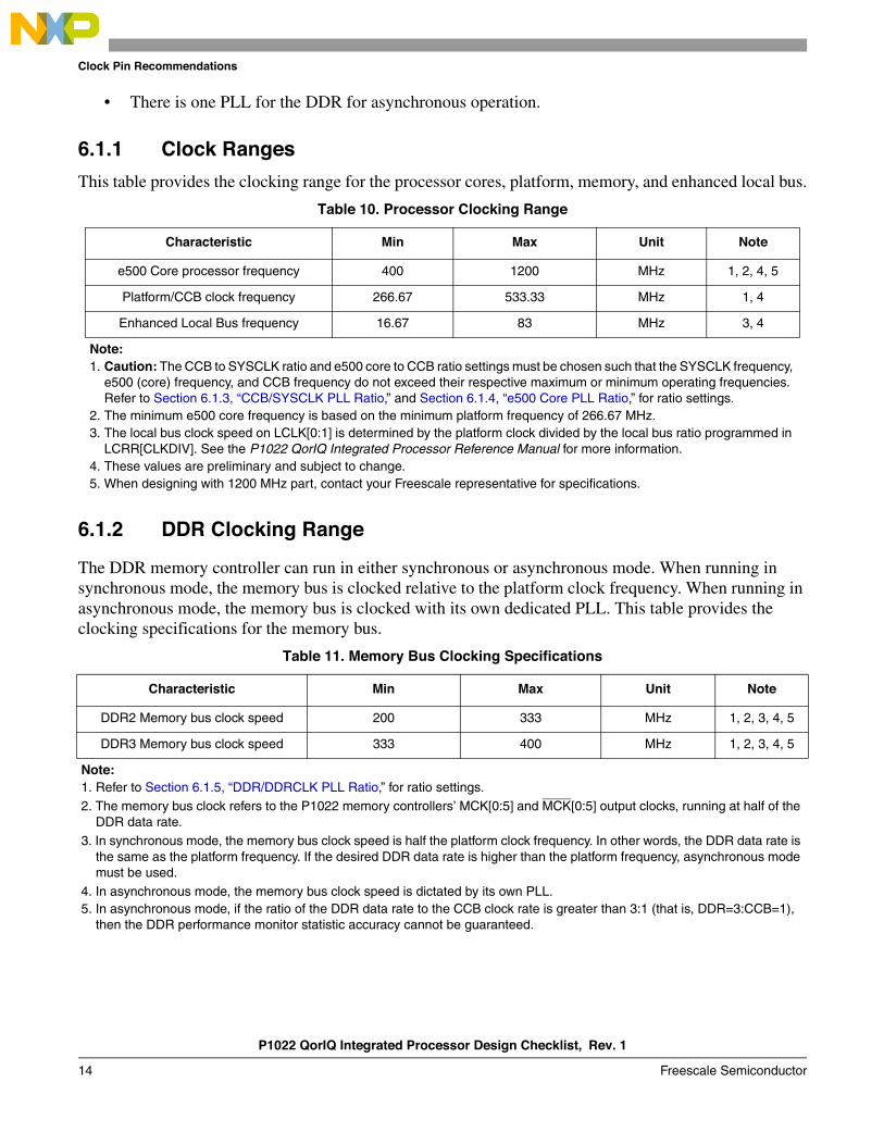
6.1.1 Clock Ranges
This table provides the clocking range for the processor cores, platform, memory, and enhanced local bus.
6.1.2 DDR Clocking Range
The DDR memory controller can run in either synchronous or asynchronous mode. When running in synchronous mode, the memory bus is clocked relative to the platform clock frequency. When running in asynchronous mode, the memory bus is clocked with its own dedicated PLL. This table provides the clocking specifications for the memory bus.
Table 10. Processor Clocking Range
Characteristic Min Max Unit Note
e500 Core processor frequency 400 1200 MHz 1, 2, 4, 5
Platform/CCB clock frequency 266.67 533.33 MHz 1, 4
Enhanced Local Bus frequency 16.67 83 MHz 3, 4
Note:
1. Caution: The CCB to SYSCLK ratio and e500 core to CCB ratio settings must be chosen such that the SYSCLK frequency, e500 (core) frequency, and CCB frequency do not exceed their respective maximum or minimum operating frequencies. Refer to Section 6.1.3, “CCB/SYSCLK PLL Ratio,” and Section 6.1.4, “e500 Core PLL Ratio,” for ratio settings.
2. The minimum e500 core frequency is based on the minimum platform frequency of 266.67 MHz.3. The local bus clock speed on LCLK[0:1] is determined by the platform clock divided by the local bus ratio programmed in
LCRR[CLKDIV]. See the P1022 QorIQ Integrated Processor Reference Manual for more information.4. These values are preliminary and subject to change.5. When designing with 1200 MHz part, contact your Freescale representative for specifications.
Table 11. Memory Bus Clocking Specifications
Characteristic Min Max Unit Note
DDR2 Memory bus clock speed 200 333 MHz 1, 2, 3, 4, 5
DDR3 Memory bus clock speed 333 400 MHz 1, 2, 3, 4, 5
Note:
1. Refer to Section 6.1.5, “DDR/DDRCLK PLL Ratio,” for ratio settings.2. The memory bus clock refers to the P1022 memory controllers’ MCK[0:5] and MCK[0:5] output clocks, running at half of the
DDR data rate.3. In synchronous mode, the memory bus clock speed is half the platform clock frequency. In other words, the DDR data rate is
the same as the platform frequency. If the desired DDR data rate is higher than the platform frequency, asynchronous mode must be used.
4. In asynchronous mode, the memory bus clock speed is dictated by its own PLL. 5. In asynchronous mode, if the ratio of the DDR data rate to the CCB clock rate is greater than 3:1 (that is, DDR=3:CCB=1),
then the DDR performance monitor statistic accuracy cannot be guaranteed.
P1022 QorIQ Integrated Processor Design Checklist, Rev. 1
Freescale Semiconductor 15
Clock Pin Recommendations
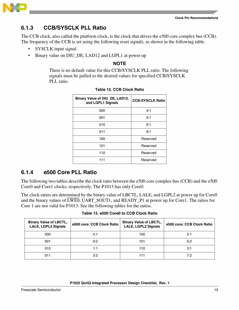
6.1.3 CCB/SYSCLK PLL Ratio
The CCB clock, also called the platform clock, is the clock that drives the e500 core complex bus (CCB). The frequency of the CCB is set using the following reset signals, as shown in the following table.
• SYSCLK input signal
• Binary value on DIU_DE, LAD12 and LGPL1 at power up
NOTE
There is no default value for this CCB/SYSCLK PLL ratio. The following signals must be pulled to the desired values for specified CCB/SYSCLK PLL ratio.
6.1.4 e500 Core PLL Ratio
The following two tables describe the clock ratio between the e500 core complex bus (CCB) and the e500 Core0 and Core1 clocks, respectively. The P1013 has only Core0.
The clock ratios are determined by the binary value of LBCTL, LALE, and LGPL2 at power up for Core0 and the binary values of LWE0, UART_SOUT1, and READY_P1 at power up for Core1. The ratios for Core 1 are not valid for P1013. See the following tables for the ratios.
Table 12. CCB Clock Ratio
Binary Value of DIU_DE, LAD12, and LGPL1 Signals
CCB:SYSCLK Ratio
000 4:1
001 5:1
010 6:1
011 8:1
100 Reserved
101 Reserved
110 Reserved
111 Reserved
Table 13. e500 Core0 to CCB Clock Ratio
Binary Value of LBCTL, LALE, LGPL2 Signals
e500 core: CCB Clock RatioBinary Value of LBCTL, LALE, LGPL2 Signals
e500 core: CCB Clock Ratio
000 4:1 100 2:1
001 9:2 101 5:2
010 1:1 110 3:1
011 3:2 111 7:2
P1022 QorIQ Integrated Processor Design Checklist, Rev. 1
16 Freescale Semiconductor
Clock Pin Recommendations
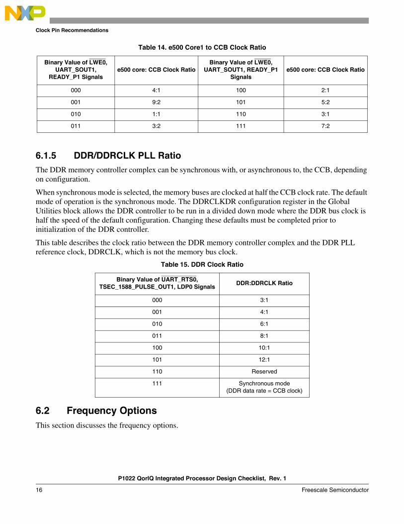
6.1.5 DDR/DDRCLK PLL Ratio
The DDR memory controller complex can be synchronous with, or asynchronous to, the CCB, depending on configuration.
When synchronous mode is selected, the memory buses are clocked at half the CCB clock rate. The default mode of operation is the synchronous mode. The DDRCLKDR configuration register in the Global Utilities block allows the DDR controller to be run in a divided down mode where the DDR bus clock is half the speed of the default configuration. Changing these defaults must be completed prior to initialization of the DDR controller.
This table describes the clock ratio between the DDR memory controller complex and the DDR PLL reference clock, DDRCLK, which is not the memory bus clock.
6.2 Frequency Options
This section discusses the frequency options.
Table 14. e500 Core1 to CCB Clock Ratio
Binary Value of LWE0, UART_SOUT1,
READY_P1 Signalse500 core: CCB Clock Ratio
Binary Value of LWE0, UART_SOUT1, READY_P1
Signalse500 core: CCB Clock Ratio
000 4:1 100 2:1
001 9:2 101 5:2
010 1:1 110 3:1
011 3:2 111 7:2
Table 15. DDR Clock Ratio
Binary Value of UART_RTS0, TSEC_1588_PULSE_OUT1, LDP0 Signals
DDR:DDRCLK Ratio
000 3:1
001 4:1
010 6:1
011 8:1
100 10:1
101 12:1
110 Reserved
111 Synchronous mode(DDR data rate = CCB clock)
P1022 QorIQ Integrated Processor Design Checklist, Rev. 1
Freescale Semiconductor 17
Clock Pin Recommendations
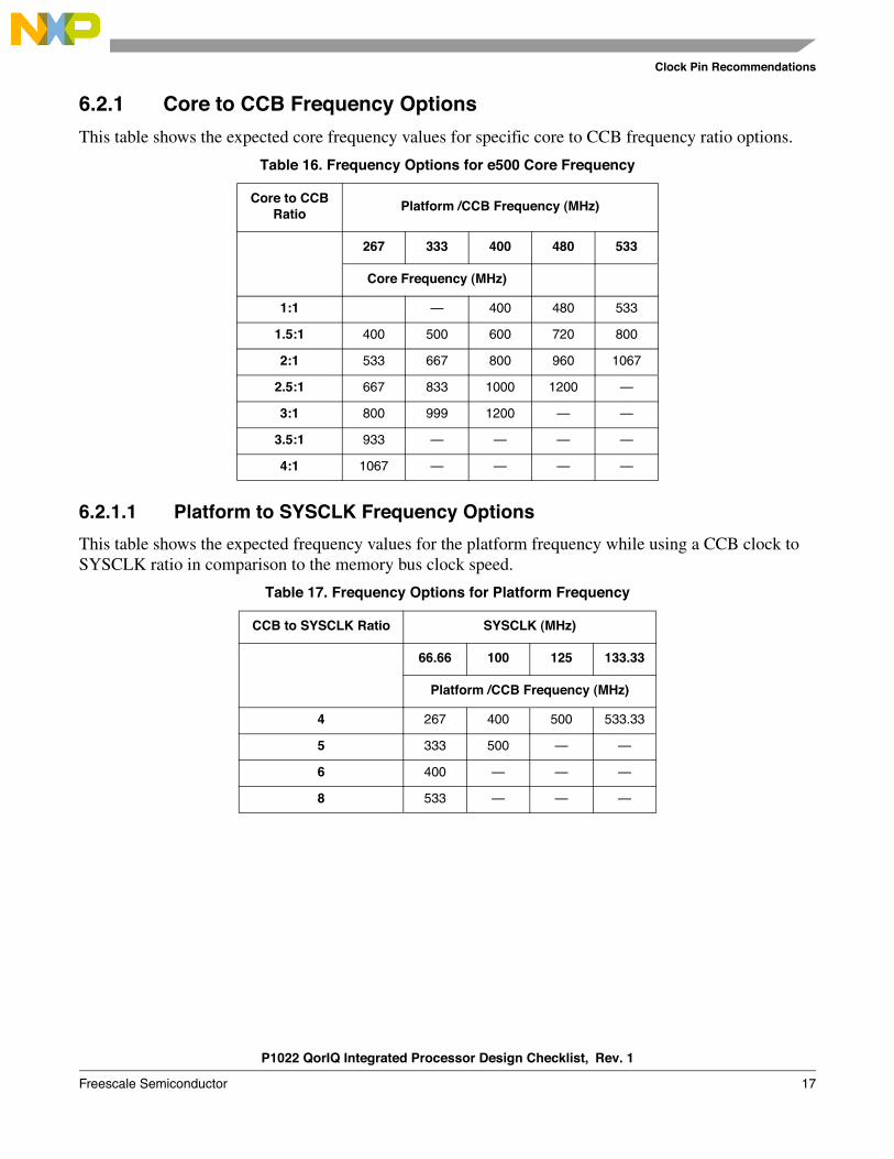
6.2.1 Core to CCB Frequency Options
This table shows the expected core frequency values for specific core to CCB frequency ratio options.
6.2.1.1 Platform to SYSCLK Frequency Options
This table shows the expected frequency values for the platform frequency while using a CCB clock to SYSCLK ratio in comparison to the memory bus clock speed.
Table 16. Frequency Options for e500 Core Frequency
Core to CCB Ratio
Platform /CCB Frequency (MHz)
267 333 400 480 533
Core Frequency (MHz)
1:1 — 400 480 533
1.5:1 400 500 600 720 800
2:1 533 667 800 960 1067
2.5:1 667 833 1000 1200 —
3:1 800 999 1200 — —
3.5:1 933 — — — —
4:1 1067 — — — —
Table 17. Frequency Options for Platform Frequency
CCB to SYSCLK Ratio SYSCLK (MHz)
66.66 100 125 133.33
Platform /CCB Frequency (MHz)
4 267 400 500 533.33
5 333 500 — —
6 400 — — —
8 533 — — —
P1022 QorIQ Integrated Processor Design Checklist, Rev. 1
18 Freescale Semiconductor
Clock Pin Recommendations
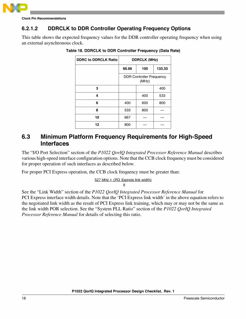
6.2.1.2 DDRCLK to DDR Controller Operating Frequency Options
This table shows the expected frequency values for the DDR controller operating frequency when using an external asynchronous clock.
6.3 Minimum Platform Frequency Requirements for High-Speed Interfaces
The “I/O Port Selection” section of the P1022 QorIQ Integrated Processor Reference Manual describes various high-speed interface configuration options. Note that the CCB clock frequency must be considered for proper operation of such interfaces as described below.
For proper PCI Express operation, the CCB clock frequency must be greater than:
527 MHz × (PCI Express link width)8
See the “Link Width” section of the P1022 QorIQ Integrated Processor Reference Manual for PCI Express interface width details. Note that the ‘PCI Express link width’ in the above equation refers to the negotiated link width as the result of PCI Express link training, which may or may not be the same as the link width POR selection. See the “System PLL Ratio” section of the P1022 QorIQ Integrated Processor Reference Manual for details of selecting this ratio.
Table 18. DDRCLK to DDR Controller Frequency (Data Rate)
DDRC to DDRCLK Ratio DDRCLK (MHz)
66.66 100 133.33
DDR Controller Frequency (MHz)
3 400
4 400 533
6 400 600 800
8 533 800 —
10 667 — —
12 800 — —
P1022 QorIQ Integrated Processor Design Checklist, Rev. 1
Freescale Semiconductor 19
DDR Interface Pin Recommendations
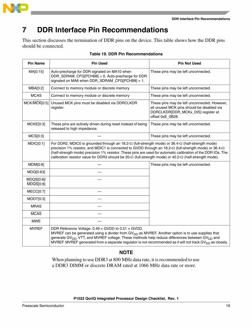
7 DDR Interface Pin Recommendations
This section discusses the termination of DDR pins on the device. This table shows how the DDR pins should be connected.
NOTE
When planning to use DDR3 at 800 MHz data rate, it is recommended to use a DDR3 DIMM or discrete DRAM rated at 1066 MHz data rate or more.
Table 19. DDR Pin Recommendations
Pin Name Pin Used Pin Not Used
MA[0:15] Auto-precharge for DDR signaled on MA10 when DDR_SDRAM_CFG[PCHB8] = 0. Auto-precharge for DDR signaled on MA8 when DDR_SDRAM_CFG[PCHB8] = 1.
These pins may be left unconnected.
MBA[0:2] Connect to memory module or discrete memory These pins may be left unconnected.
MCAS Connect to memory module or discrete memory These pins may be left unconnected.
MCK/MCK[0:5] Unused MCK pins must be disabled via DDRCLKDR register.
These pins may be left unconnected. However, all unused MCK pins should be disabled via DDRCLKDR[DDR_MCKx_DIS] register at offset 0xE_0B28.
MCKE[0:3] These pins are actively driven during reset instead of being released to high impedance.
These pins may be left unconnected.
MCS[0:3] — These pins may be left unconnected.
MDIC[0:1] For DDR2, MDIC0 is grounded through an 18.2- (full-strength mode) or 36.4- (half-strength mode) precision 1% resistor, and MDIC1 is connected to GVDD through an 18.2- (full-strength mode) or 36.4- (half-strength mode) precision 1% resistor. These pins are used for automatic calibration of the DDR IOs. The calibration resistor value for DDR3 should be 20- (full-strength mode) or 40.2- (half-strength mode).
MDM[0:8] — These pins may be left unconnected.
MDQ[0:63] —
MDQS[0:8]/ MDQS[0:8]
—
MECC[0:7] —
MODT[0:3] —
MRAS —
MCAS —
MWE —
MVREF DDR Reference Voltage: 0.49 × GVDD to 0.51 × GVDD.MVREF can be generated using a divider from GVDD as MVREF. Another option is to use supplies that generate GVDD, VTT, and MVREF voltage. These methods help reduce differences between GVDD and MVREF. MVREF generated from a separate regulator is not recommended as it will not track GVDD as closely.
P1022 QorIQ Integrated Processor Design Checklist, Rev. 1
20 Freescale Semiconductor
DUART, IIC, and SSI Interface Pin Recommendations
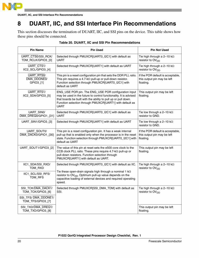
8 DUART, IIC, and SSI Interface Pin Recommendations
This section discusses the termination of DUART, IIC, and SSI pins on the device. This table shows how these pins should be connected.
Table 20. DUART, IIC and SSI Pin Recommendations
Pin Name Pin Used Pin Not Used
UART_CTS0/SSI_RCK/TDM_RCLK/GPIO3_[0]
Selected through PMUXCR[UART0_I2C1] with default as UART
Tie high through a 2–10 k resistor to OVDD
UART_CTS1/ IIC2_SCL/GPIO3_[4]
Selected through PMUXCR[UART1] with default as UART Tie high through a 2–10 k resistor to OVDD.
UART_RTS0/ DMA_DDONE0/
GPIO3_[1]
This pin is a reset configuration pin that sets the DDR PLL ratio. This pin requires a 4.7-k pull-up or pull-down resistor. Function selection through PMUXCR[UART0_I2C1] with default as UART
If the POR default is acceptable, this output pin may be left floating.
UART_RTS1/ IIC2_SDA/GPIO3_[5]
ENG_USE POR pin. The ENG_USE POR configuration input may be used in the future to control functionality. It is advised that boards be built with the ability to pull up or pull down. Function selection through PMUXCR[UART1] with default as UART
This output pin may be left floating.
UART_SIN0/DMA_DREQ0/GPIO1_[31]
Selected through PMUXCR[UART0_I2C1] with default as UART
Tie low through a 2–10 k resistor to GND.
UART_SIN1/GPIO3_[3] Selected through PMUXCR[UART1] with default as UART Tie low through a 2–10 k resistor to GND.
UART_SOUT0/DMA_DACK0/GPIO1_[30]
This pin is a reset configuration pin. It has a weak internal pull-up that is enabled only when the processor is in the reset state. Function selection through PMUXCR[UART0_I2C1] with default as UART
If the POR default is acceptable, this output pin may be left floating.
UART_SOUT1/GPIO3_[2] The value of this pin at reset sets the e500 core clock to the CCB clock PLL ratio. These pins require 4.7-k pull-up or pull-down resistors. Function selection through PMUXCR[UART1] with default as UART.
This output pin may be left floating.
IIC1_SDA/SSI_RXD/ TDM_RXD
Selected through PMUXCR[UART0_I2C1] with default as IIC.
Tie these open-drain signals high through a nominal 1 k resistor to OVDD. Optimum pull-up value depends on the capacitive loading of external devices and required operating speed.
Tie high through a 2–10 k resistor to OVDD
IIC1_SCL/SSI_RFS/ TDM_RFS
SSI_TCK/DMA_DACK1/ TDM_TCK/GPIO3_[6]
Selected through PMUXCR[SSI_DMA_TDM] with default as SSI.
Tie high through a 2–10 k resistor to OVDD
SSI_TFS/ DMA_DDONE1/ TDM_TFS/GPIO3_[7]
SSI_TXD/DMA_DREQ1/ TDM_TXD/GPIO3_[8]
This output pin may be left floating.
P1022 QorIQ Integrated Processor Design Checklist, Rev. 1
Freescale Semiconductor 21
eSDHC Interface Pin Recommendations
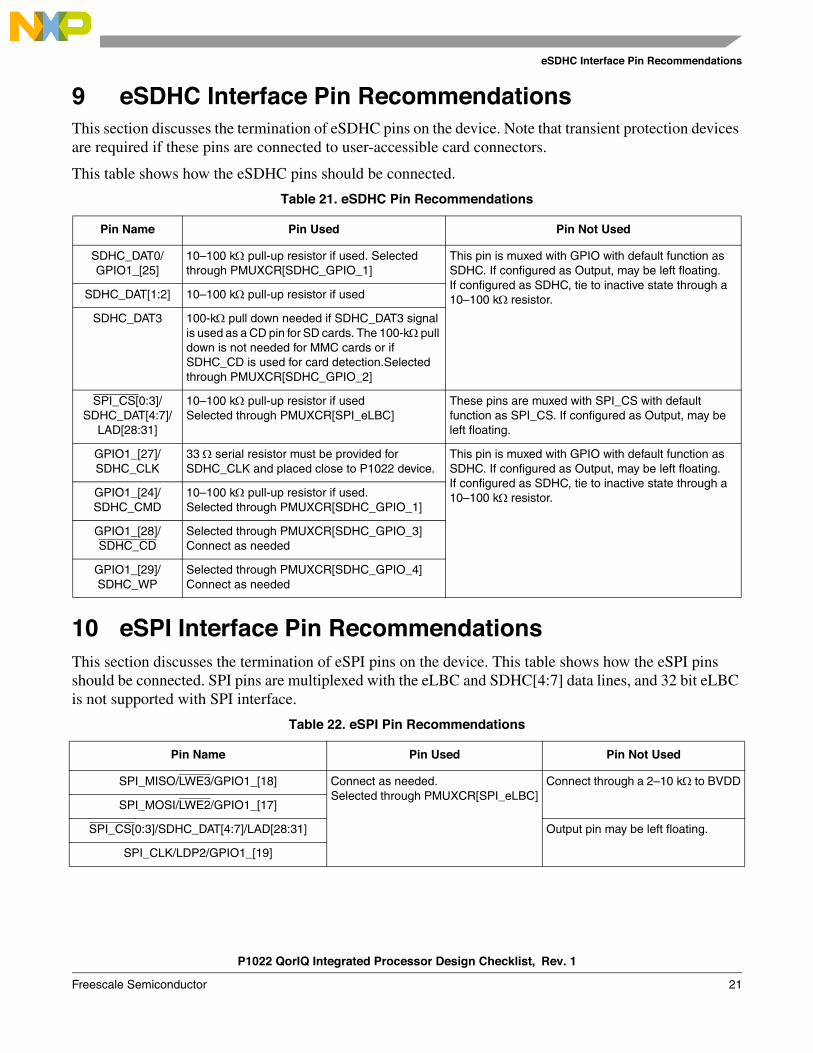
9 eSDHC Interface Pin RecommendationsThis section discusses the termination of eSDHC pins on the device. Note that transient protection devices are required if these pins are connected to user-accessible card connectors.
This table shows how the eSDHC pins should be connected.
10 eSPI Interface Pin Recommendations
This section discusses the termination of eSPI pins on the device. This table shows how the eSPI pins should be connected. SPI pins are multiplexed with the eLBC and SDHC[4:7] data lines, and 32 bit eLBC is not supported with SPI interface.
Table 21. eSDHC Pin Recommendations
Pin Name Pin Used Pin Not Used
SDHC_DAT0/GPIO1_[25]
10–100 k pull-up resistor if used. Selected through PMUXCR[SDHC_GPIO_1]
This pin is muxed with GPIO with default function as SDHC. If configured as Output, may be left floating.If configured as SDHC, tie to inactive state through a 10–100 kresistor.SDHC_DAT[1:2] 10–100 k pull-up resistor if used
SDHC_DAT3 100-k pull down needed if SDHC_DAT3 signal is used as a CD pin for SD cards. The 100-k pull down is not needed for MMC cards or if SDHC_CD is used for card detection.Selected through PMUXCR[SDHC_GPIO_2]
SPI_CS[0:3]/SDHC_DAT[4:7]/
LAD[28:31]
10–100 k pull-up resistor if usedSelected through PMUXCR[SPI_eLBC]
These pins are muxed with SPI_CS with default function as SPI_CS. If configured as Output, may be left floating.
GPIO1_[27]/SDHC_CLK
33 serial resistor must be provided for SDHC_CLK and placed close to P1022 device.
This pin is muxed with GPIO with default function as SDHC. If configured as Output, may be left floating.If configured as SDHC, tie to inactive state through a 10–100 kresistor.GPIO1_[24]/
SDHC_CMD10–100 k pull-up resistor if used.Selected through PMUXCR[SDHC_GPIO_1]
GPIO1_[28]/SDHC_CD
Selected through PMUXCR[SDHC_GPIO_3] Connect as needed
GPIO1_[29]/SDHC_WP
Selected through PMUXCR[SDHC_GPIO_4]Connect as needed
Table 22. eSPI Pin Recommendations
Pin Name Pin Used Pin Not Used
SPI_MISO/LWE3/GPIO1_[18] Connect as needed.Selected through PMUXCR[SPI_eLBC]
Connect through a 2–10 k to BVDD
SPI_MOSI/LWE2/GPIO1_[17]
SPI_CS[0:3]/SDHC_DAT[4:7]/LAD[28:31] Output pin may be left floating.
SPI_CLK/LDP2/GPIO1_[19]
P1022 QorIQ Integrated Processor Design Checklist, Rev. 1
22 Freescale Semiconductor
USB Interface Pin Recommendations
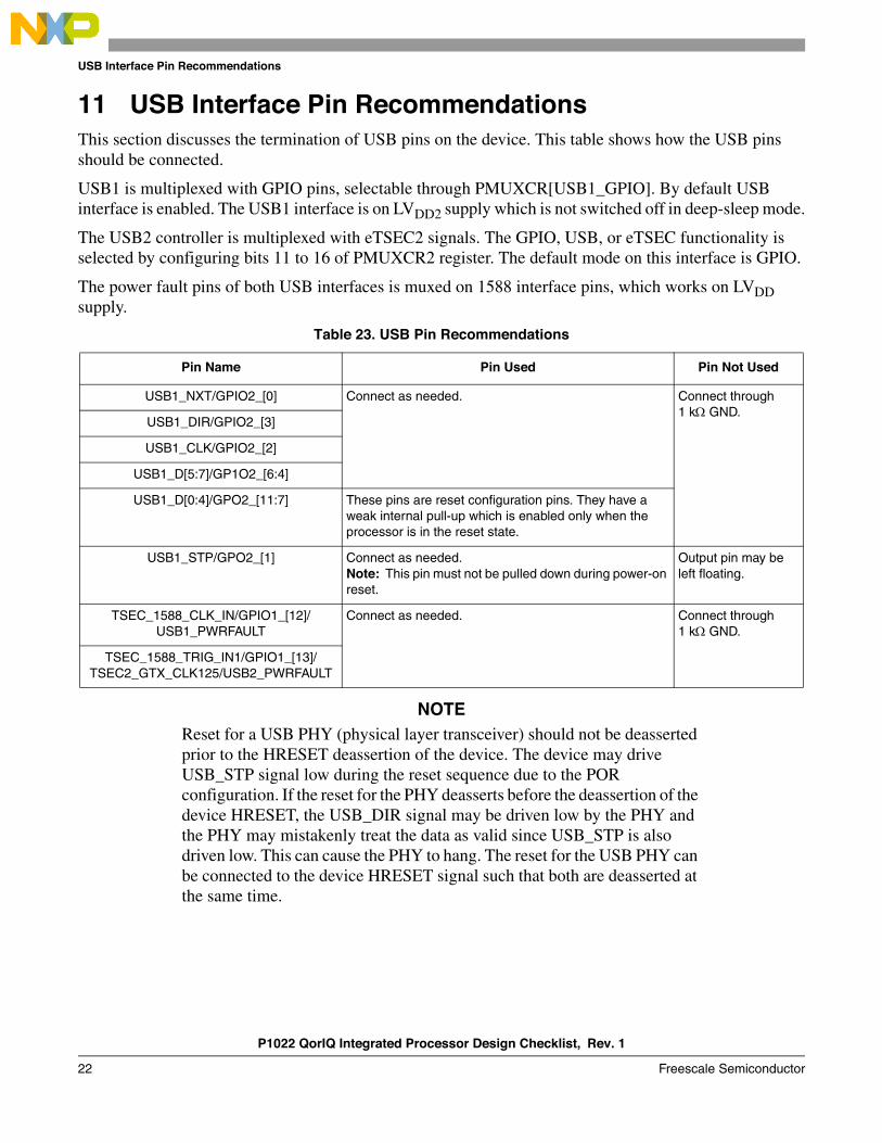
11 USB Interface Pin RecommendationsThis section discusses the termination of USB pins on the device. This table shows how the USB pins should be connected.
USB1 is multiplexed with GPIO pins, selectable through PMUXCR[USB1_GPIO]. By default USB interface is enabled. The USB1 interface is on LVDD2 supply which is not switched off in deep-sleep mode.
The USB2 controller is multiplexed with eTSEC2 signals. The GPIO, USB, or eTSEC functionality is selected by configuring bits 11 to 16 of PMUXCR2 register. The default mode on this interface is GPIO.
The power fault pins of both USB interfaces is muxed on 1588 interface pins, which works on LVDD supply.
NOTE
Reset for a USB PHY (physical layer transceiver) should not be deasserted prior to the HRESET deassertion of the device. The device may drive USB_STP signal low during the reset sequence due to the POR configuration. If the reset for the PHY deasserts before the deassertion of the device HRESET, the USB_DIR signal may be driven low by the PHY and the PHY may mistakenly treat the data as valid since USB_STP is also driven low. This can cause the PHY to hang. The reset for the USB PHY can be connected to the device HRESET signal such that both are deasserted at the same time.
Table 23. USB Pin Recommendations
Pin Name Pin Used Pin Not Used
USB1_NXT/GPIO2_[0] Connect as needed. Connect through 1 k GND.
USB1_DIR/GPIO2_[3]
USB1_CLK/GPIO2_[2]
USB1_D[5:7]/GP1O2_[6:4]
USB1_D[0:4]/GPO2_[11:7] These pins are reset configuration pins. They have a weak internal pull-up which is enabled only when the processor is in the reset state.
USB1_STP/GPO2_[1] Connect as needed. Note: This pin must not be pulled down during power-on reset.
Output pin may be left floating.
TSEC_1588_CLK_IN/GPIO1_[12]/ USB1_PWRFAULT
Connect as needed. Connect through 1 k GND.
TSEC_1588_TRIG_IN1/GPIO1_[13]/ TSEC2_GTX_CLK125/USB2_PWRFAULT
P1022 QorIQ Integrated Processor Design Checklist, Rev. 1
Freescale Semiconductor 23
Ethernet Management Interface Pin Recommendations
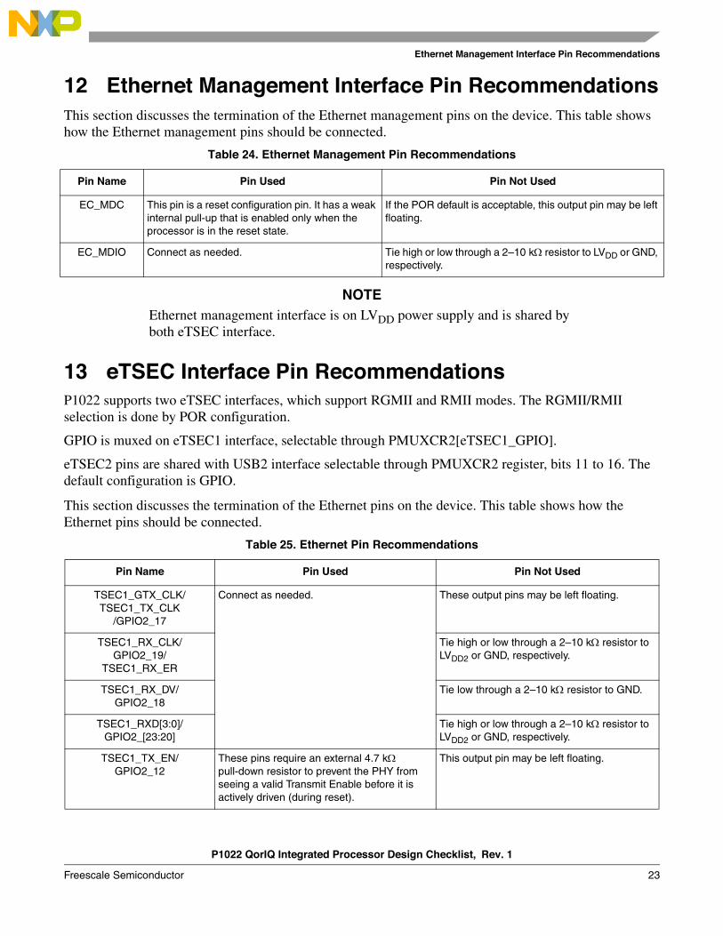
12 Ethernet Management Interface Pin Recommendations
This section discusses the termination of the Ethernet management pins on the device. This table shows how the Ethernet management pins should be connected.
NOTE
Ethernet management interface is on LVDD power supply and is shared by both eTSEC interface.
13 eTSEC Interface Pin RecommendationsP1022 supports two eTSEC interfaces, which support RGMII and RMII modes. The RGMII/RMII selection is done by POR configuration.
GPIO is muxed on eTSEC1 interface, selectable through PMUXCR2[eTSEC1_GPIO].
eTSEC2 pins are shared with USB2 interface selectable through PMUXCR2 register, bits 11 to 16. The default configuration is GPIO.
This section discusses the termination of the Ethernet pins on the device. This table shows how the Ethernet pins should be connected.
Table 24. Ethernet Management Pin Recommendations
Pin Name Pin Used Pin Not Used
EC_MDC This pin is a reset configuration pin. It has a weak internal pull-up that is enabled only when the processor is in the reset state.
If the POR default is acceptable, this output pin may be left floating.
EC_MDIO Connect as needed. Tie high or low through a 2–10 k resistor to LVDD or GND, respectively.
Table 25. Ethernet Pin Recommendations
Pin Name Pin Used Pin Not Used
TSEC1_GTX_CLK/TSEC1_TX_CLK
/GPIO2_17
Connect as needed. These output pins may be left floating.
TSEC1_RX_CLK/GPIO2_19/
TSEC1_RX_ER
Tie high or low through a 2–10 k resistor to LVDD2 or GND, respectively.
TSEC1_RX_DV/GPIO2_18
Tie low through a 2–10 k resistor to GND.
TSEC1_RXD[3:0]/GPIO2_[23:20]
Tie high or low through a 2–10 k resistor to LVDD2 or GND, respectively.
TSEC1_TX_EN/GPIO2_12
These pins require an external 4.7 k pull-down resistor to prevent the PHY from seeing a valid Transmit Enable before it is actively driven (during reset).
This output pin may be left floating.
P1022 QorIQ Integrated Processor Design Checklist, Rev. 1
24 Freescale Semiconductor
JTAG Interface Pin Recommendations
NOTE
eTSEC1 interface is on LVDD2 power supply rail and eTSEC2 on LVDD supply. The voltage level selection is through LVDD_VSEL, which is single control for both power supplies.
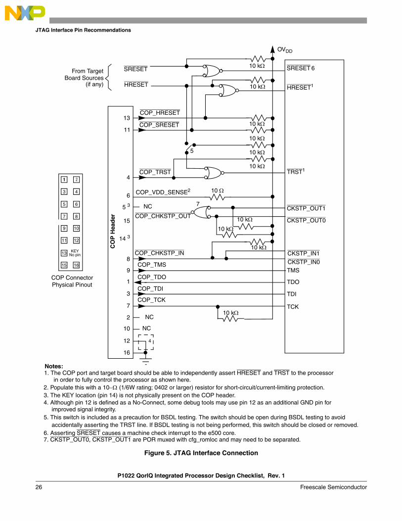
14 JTAG Interface Pin RecommendationsCorrect operation of the JTAG interface requires configuration of a group of system control pins as demonstrated in Figure 4. Care must be taken to ensure that these pins are maintained at a valid deasserted state under normal operating conditions, as most have asynchronous behavior and spurious assertion will give unpredictable results.
Boundary-scan testing is enabled through the JTAG interface signals. The TRST signal is optional in the IEEE Std 1149.1 specification, but it is provided on all processors built on Power Architecture technology. The device requires TRST to be asserted during power-on reset flow to ensure that the JTAG boundary logic does not interfere with normal chip operation. While the TAP controller can be forced to the reset state using only the TCK and TMS signals, generally systems assert TRST during the power-on reset flow. Simply tying TRST to HRESET is not practical because the JTAG interface is also used for accessing the common on-chip processor (COP), which implements the debug interface to the chip.
TSEC1_TXD[3:0]/GPIO2_[16:13]
These pins are reset configuration pins. They have a weak internal pull-up that is enabled only when the processor is in the reset state.
If the POR default is acceptable, these output pins may be left floating.TSEC1_TXD3 must not be pulled down during POR.
TSEC1_GTX_CLK125]/GPIO2_24
See Table 9
TSEC2_GTX_CLK/TSEC2_TX_CLK/
GPIO1_[15]/ USB2_CLK
Connect as needed. Selected through PMUXCR2[eTSEC2_USB3].
The default function of these pins is GPIO. If configured as output, they may be left floating.
TSEC2_RX_CLK/TSEC2_RX_ER/GPIO1_[7]
TSEC2_RX_DV/GPIO1_[6]
Connect as needed. Selected through PMUXCR2[eTSEC2_USB1].
TSEC2_RXD[1:0]/GPIO1_[9:8]/USB2_D[1:0]
TSEC2_TX_EN/GPIO1_[10]/USB2_STP
TSEC2_TXD[1:0]/GPIO1_[2:1]/USB2_D[5:4]
TSEC2_TXD[3:2]/GPIO1_[4:3]/USB2_D[7:6]
Connect as needed. Selected through PMUXCR2[eTSEC2_USB2].
TSEC2_RXD[3:2]/GPIO1_[11:10]/USB2_D[3:2]
Table 25. Ethernet Pin Recommendations (continued)
Pin Name Pin Used Pin Not Used
P1022 QorIQ Integrated Processor Design Checklist, Rev. 1
Freescale Semiconductor 25
JTAG Interface Pin Recommendations
The COP function of these processors allow a remote computer system (typically, a PC with dedicated hardware and debugging software) to access and control the internal operations of the processor. The COP interface connects primarily through the JTAG port of the processor, with some additional status monitoring signals. The COP port requires the ability to independently assert HRESET and TRST in order to fully control the processor. If the target system has independent reset sources, such as voltage monitors, watchdog timers, power supply failures, or push-button switches, then the COP reset signals must be merged along with these signals with logic.
The arrangement shown in Figure 4 allows the COP port to independently assert HRESET or TRST while ensuring that the target can drive HRESET as well.
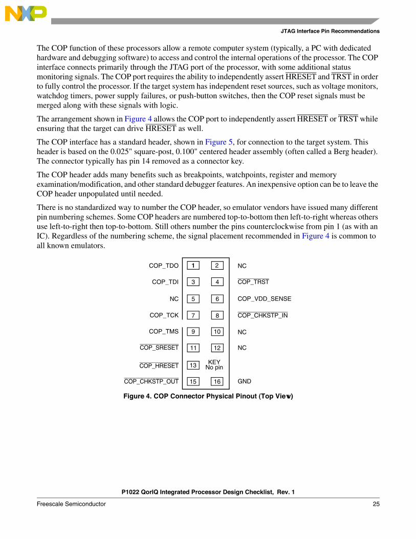
The COP interface has a standard header, shown in Figure 5, for connection to the target system. This header is based on the 0.025" square-post, 0.100" centered header assembly (often called a Berg header). The connector typically has pin 14 removed as a connector key.
The COP header adds many benefits such as breakpoints, watchpoints, register and memory examination/modification, and other standard debugger features. An inexpensive option can be to leave the COP header unpopulated until needed.
There is no standardized way to number the COP header, so emulator vendors have issued many different pin numbering schemes. Some COP headers are numbered top-to-bottom then left-to-right whereas others use left-to-right then top-to-bottom. Still others number the pins counterclockwise from pin 1 (as with an IC). Regardless of the numbering scheme, the signal placement recommended in Figure 4 is common to all known emulators.
Figure 4. COP Connector Physical Pinout (Top View)
3
13
9
5
1
6
10
15
11
7
16
12
8
4
KEYNo pin
1 2COP_TDO
COP_TDI
NC
NC
COP_TRST
COP_VDD_SENSE
COP_CHKSTP_IN
NC
NC
GND
COP_TCK
COP_TMS
COP_SRESET
COP_HRESET
COP_CHKSTP_OUT
P1022 QorIQ Integrated Processor Design Checklist, Rev. 1
26 Freescale Semiconductor
JTAG Interface Pin Recommendations
Figure 5. JTAG Interface Connection
HRESET
From TargetBoard Sources
COP_HRESET13
COP_SRESET
SRESET
NC
11
COP_VDD_SENSE26
5 3
15
10
10 k
10 k
COP_CHKSTP_IN
CKSTP_IN08COP_TMS
COP_TDO
COP_TDI
COP_TCK
TMS
TDO
TDI
9
1
3
4COP_TRST
7
16
2
10
12
(if any)
CO
P H
ead
er
14 3
Notes:
3. The KEY location (pin 14) is not physically present on the COP header.
10 k
TRST110 k
10 k
10 k
CKSTP_OUT0COP_CHKSTP_OUT
3
13
9
5
1
6
10
15
11
7
16
12
8
4
KEYNo pin
COP ConnectorPhysical Pinout
1 2
NC
SRESET
2. Populate this with a 10 (1/6W rating; 0402 or larger) resistor for short-circuit/current-limiting protection.
NC
OVDD
10 k
10 k HRESET1
in order to fully control the processor as shown here.
4. Although pin 12 is defined as a No-Connect, some debug tools may use pin 12 as an additional GND pin for
1. The COP port and target board should be able to independently assert HRESET and TRST to the processor
improved signal integrity.
TCK
4
5
5. This switch is included as a precaution for BSDL testing. The switch should be open during BSDL testing to avoidaccidentally asserting the TRST line. If BSDL testing is not being performed, this switch should be closed or removed.
10 k
6
6. Asserting SRESET causes a machine check interrupt to the e500 core.
CKSTP_OUT1
CKSTP_IN1
10 k
7
7. CKSTP_OUT0, CKSTP_OUT1 are POR muxed with cfg_romloc and may need to be separated.
P1022 QorIQ Integrated Processor Design Checklist, Rev. 1
Freescale Semiconductor 27
eLBC Interface Pin Recommendations
14.1 JTAG Pin Recommendations
If the JTAG interface and COP header are not used, Freescale recommends the following connections:
• TRST should be tied to HRESET through a 0- isolation resistor so that it is asserted when the system reset signal (HRESET) is asserted, ensuring that the JTAG scan chain is initialized during the power-on reset flow. Freescale recommends that the COP header be designed into the system as shown in Figure 5. If this is not possible, the isolation resistor will allow future access to TRST in case a JTAG interface may need to be wired onto the system in future debug situations.
• No pull-up/pull-down is required for TDI, TMS, or TDO.
This table shows how the JTAG pins should be connected.
15 eLBC Interface Pin RecommendationsThe eLBC, DIU, SPI, and eSDHC interfaces are muxed in P1022. The eLBC can support 32-bit (address and data), 28-bit address/16-bit data or 24-bit address/16-bit data configurations. In addition 8 or 16 bit NAND interface is also supported on eLBC. The DIU pins are shared with eLBC, which limit the usage of eLBC. When enabled through PMUXCR register, 8bit address/data and only 2 chip selects are supported on eLBC. Refer to the P1022 QorIQ Integrated Processor Reference Manual for details.
The eLBC and SPI pins are on BVDD supply which can be 3.3/2.5/1.8V while the eSDHC is on OVDD supply which can be 3.3V only. With eSDHC in 8-bit mode, BVDD should be 3.3V which restricts eLBC to 3.3V only.
Table 26. JTAG Pin Recommendations
Pin Name Pin Used Pin Not Used
TCK If COP is used, connect as needed and strap to OVDD2 via a 10 k pull up.
If COP is unused, tie TCK to OVDD2 through a 10 kresistor. This prevents TCK from changing state and reading incorrect data into the device.
TDI This pin has a weak internal pull-up that is always enabled. Connect to Pin3 of the COP connector.
This pin may be left unconnected.
TDO Connect to Pin1 of the COP connector. This pin may be left unconnected.
TMS This pin has a weak internal pull-up that is always enabled. Connect to Pin9 of the COP connector.
This pin may be left unconnected.
TRST Connect as shown in Figure 5. TRST should be tied to HRESET through a 0- resistor.
P1022 QorIQ Integrated Processor Design Checklist, Rev. 1
28 Freescale Semiconductor
eLBC Interface Pin Recommendations
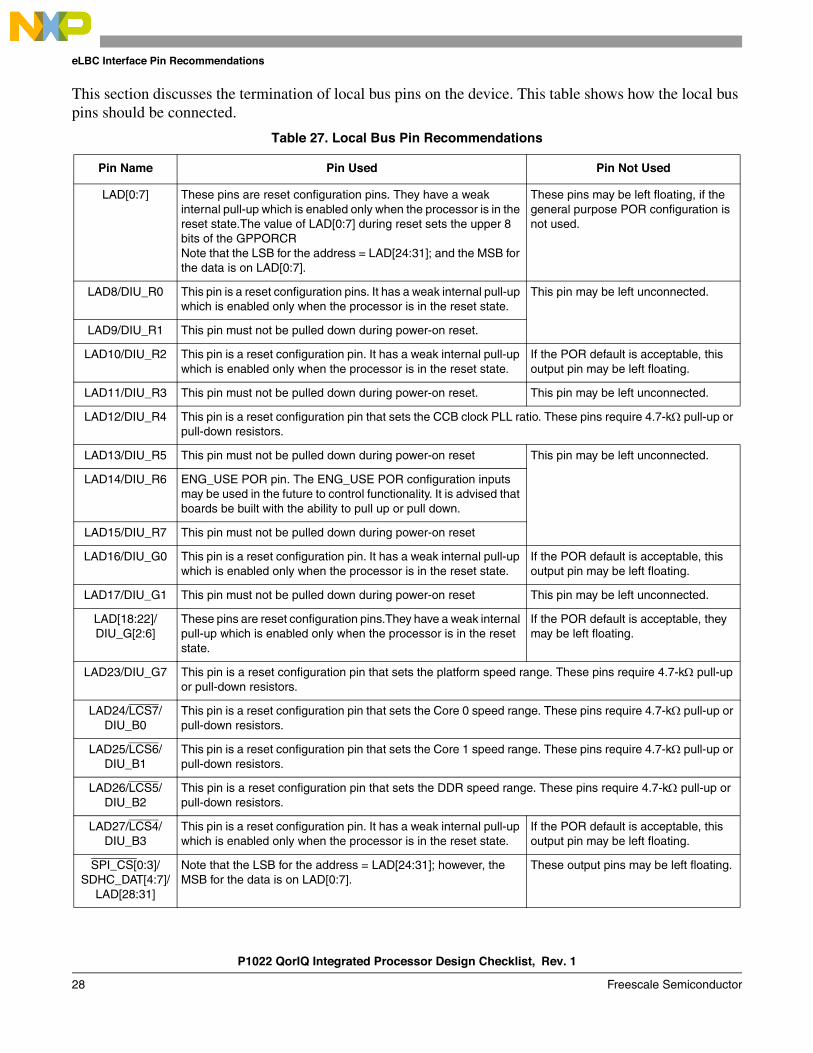
This section discusses the termination of local bus pins on the device. This table shows how the local bus pins should be connected.
Table 27. Local Bus Pin Recommendations
Pin Name Pin Used Pin Not Used
LAD[0:7] These pins are reset configuration pins. They have a weak internal pull-up which is enabled only when the processor is in the reset state.The value of LAD[0:7] during reset sets the upper 8 bits of the GPPORCRNote that the LSB for the address = LAD[24:31]; and the MSB for the data is on LAD[0:7].
These pins may be left floating, if the general purpose POR configuration is not used.
LAD8/DIU_R0 This pin is a reset configuration pins. It has a weak internal pull-up which is enabled only when the processor is in the reset state.
This pin may be left unconnected.
LAD9/DIU_R1 This pin must not be pulled down during power-on reset.
LAD10/DIU_R2 This pin is a reset configuration pin. It has a weak internal pull-up which is enabled only when the processor is in the reset state.
If the POR default is acceptable, this output pin may be left floating.
LAD11/DIU_R3 This pin must not be pulled down during power-on reset. This pin may be left unconnected.
LAD12/DIU_R4 This pin is a reset configuration pin that sets the CCB clock PLL ratio. These pins require 4.7-k pull-up or pull-down resistors.
LAD13/DIU_R5 This pin must not be pulled down during power-on reset This pin may be left unconnected.
LAD14/DIU_R6 ENG_USE POR pin. The ENG_USE POR configuration inputs may be used in the future to control functionality. It is advised that boards be built with the ability to pull up or pull down.
LAD15/DIU_R7 This pin must not be pulled down during power-on reset
LAD16/DIU_G0 This pin is a reset configuration pin. It has a weak internal pull-up which is enabled only when the processor is in the reset state.
If the POR default is acceptable, this output pin may be left floating.
LAD17/DIU_G1 This pin must not be pulled down during power-on reset This pin may be left unconnected.
LAD[18:22]/ DIU_G[2:6]
These pins are reset configuration pins.They have a weak internal pull-up which is enabled only when the processor is in the reset state.
If the POR default is acceptable, they may be left floating.
LAD23/DIU_G7 This pin is a reset configuration pin that sets the platform speed range. These pins require 4.7-k pull-up or pull-down resistors.
LAD24/LCS7/ DIU_B0
This pin is a reset configuration pin that sets the Core 0 speed range. These pins require 4.7-k pull-up or pull-down resistors.
LAD25/LCS6/ DIU_B1
This pin is a reset configuration pin that sets the Core 1 speed range. These pins require 4.7-k pull-up or pull-down resistors.
LAD26/LCS5/ DIU_B2
This pin is a reset configuration pin that sets the DDR speed range. These pins require 4.7-k pull-up or pull-down resistors.
LAD27/LCS4/ DIU_B3
This pin is a reset configuration pin. It has a weak internal pull-up which is enabled only when the processor is in the reset state.
If the POR default is acceptable, this output pin may be left floating.
SPI_CS[0:3]/ SDHC_DAT[4:7]/
LAD[28:31]
Note that the LSB for the address = LAD[24:31]; however, the MSB for the data is on LAD[0:7].
These output pins may be left floating.
P1022 QorIQ Integrated Processor Design Checklist, Rev. 1
Freescale Semiconductor 29
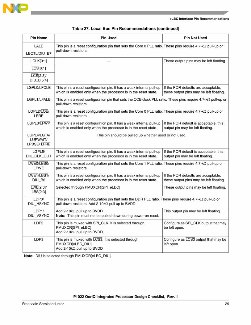
eLBC Interface Pin Recommendations
LALE This pin is a reset configuration pin that sets the Core 0 PLL ratio. These pins require 4.7-k pull-up or pull-down resistors.
LBCTL/DIU_B7
LCLK[0:1] — These output pins may be left floating.
LCS[0:1]
LCS[2:3]/ DIU_B[5:4]
LGPL0/LFCLE This pin is a reset configuration pin. It has a weak internal pull-up which is enabled only when the processor is in the reset state.
If the POR defaults are acceptable, these output pins may be left floating.
LGPL1/LFALE This pin is a reset configuration pin that sets the CCB clock PLL ratio. These pins require 4.7-k pull-up or pull-down resistors.
LGPL2/LOE/LFRE
This pin is a reset configuration pin that sets the Core 0 PLL ratio. These pins require 4.7-k pull-up or pull-down resistors.
LGPL3/LFWP This pin is a reset configuration pin. It has a weak internal pull-up which is enabled only when the processor is in the reset state.
If the POR default is acceptable, this output pin may be left floating.
LGPL4/LGTA/LUPWAIT/
LPBSE/ LFRB
This pin should be pulled up whether used or not used.
LGPL5/ DIU_CLK_OUT
This pin is a reset configuration pin. It has a weak internal pull-up which is enabled only when the processor is in the reset state.
If the POR default is acceptable, this output pin may be left floating.
LWE0/LBS0/LFWE
This pin is a reset configuration pin that sets the Core 1 PLL ratio. These pins require 4.7-k pull-up or pull-down resistors.
LWE1/LBS1/ DIU_B6
This pin is a reset configuration pin. It has a weak internal pull-up which is enabled only when the processor is in the reset state.
If the POR defaults are acceptable, these output pins may be left floating
LWE[2:3]/ LBS[2:3]
Selected through PMUXCR[SPI_eLBC] These output pins may be left floating.
LDP0/ DIU_HSYNC
This pin is a reset configuration pin that sets the DDR PLL ratio. These pins require 4.7-k pull-up or pull-down resistors. Add 2-10kpull up to BVDD
LDP1/ DIU_VSYNC
Add 2-10kpull up to BVDDNote: This pin must not be pulled down during power-on reset.
This output pin may be left floating.
LDP2 This pin is muxed with SPI_CLK. It is selected through PMUXCR[SPI_eLBC]Add 2-10k pull up to BVDD
Configure as SPI_CLK output that may be left open.
LDP3 This pin is muxed with LCS3. It is selected through PMUXCR[eLBC_DIU]Add 2-10k pull up to BVDD
Configure as LCS3 output that may be left open.
Note: DIU is selected through PMUXCR[eLBC_DIU].
Table 27. Local Bus Pin Recommendations (continued)
Pin Name Pin Used Pin Not Used
P1022 QorIQ Integrated Processor Design Checklist, Rev. 1
30 Freescale Semiconductor
eLBC Interface Pin Recommendations
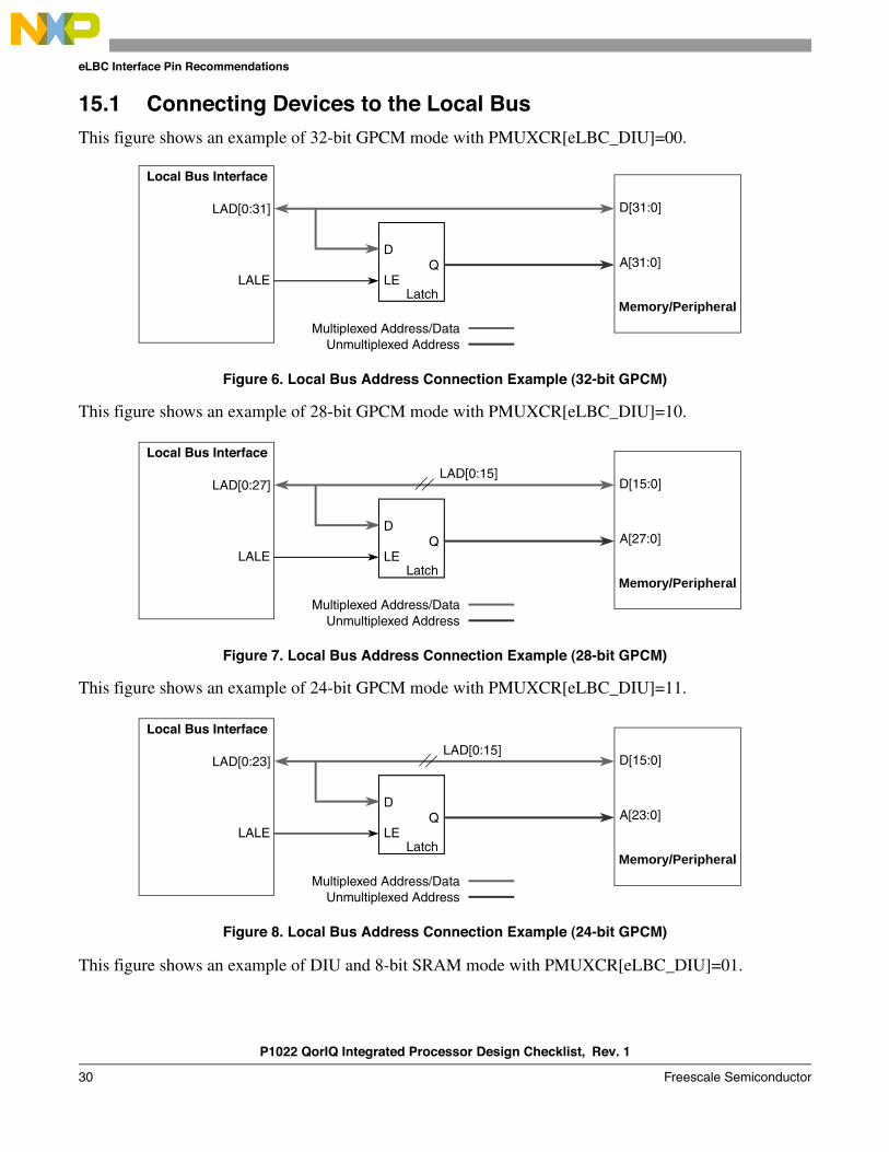
15.1 Connecting Devices to the Local Bus
This figure shows an example of 32-bit GPCM mode with PMUXCR[eLBC_DIU]=00.
Figure 6. Local Bus Address Connection Example (32-bit GPCM)
This figure shows an example of 28-bit GPCM mode with PMUXCR[eLBC_DIU]=10.
Figure 7. Local Bus Address Connection Example (28-bit GPCM)
This figure shows an example of 24-bit GPCM mode with PMUXCR[eLBC_DIU]=11.
Figure 8. Local Bus Address Connection Example (24-bit GPCM)
This figure shows an example of DIU and 8-bit SRAM mode with PMUXCR[eLBC_DIU]=01.
Multiplexed Address/DataUnmultiplexed Address
LALE
Local Bus Interface
Latch
DQ
LE
LAD[0:31]
A[31:0]
D[31:0]
Memory/Peripheral
Multiplexed Address/DataUnmultiplexed Address
LALE
Local Bus Interface
Latch
DQ
LE
LAD[0:27]
A[27:0]
D[15:0]
Memory/Peripheral
LAD[0:15]
Multiplexed Address/DataUnmultiplexed Address
LALE
Local Bus Interface
Latch
DQ
LE
LAD[0:23]
A[23:0]
D[15:0]
Memory/Peripheral
LAD[0:15]
P1022 QorIQ Integrated Processor Design Checklist, Rev. 1
Freescale Semiconductor 31
PIC Interface Pin Recommendations
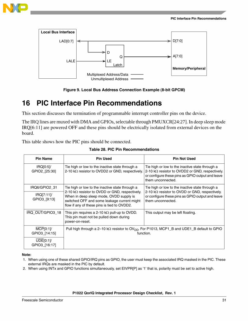
Figure 9. Local Bus Address Connection Example (8-bit GPCM)
16 PIC Interface Pin Recommendations
This section discusses the termination of programmable interrupt controller pins on the device.
The IRQ lines are muxed with DMA and GPIOs, selectable through PMUXCR[24:27]. In deep sleep mode IRQ[6:11] are powered OFF and these pins should be electrically isolated from external devices on the board.
This table shows how the PIC pins should be connected.
Note:
1. When using one of these shared GPIO/IRQ pins as GPIO, the user must keep the associated IRQ masked in the PIC. These external IRQs are masked in the PIC by default.
2. When using INTx and GPIO functions simultaneously, set EIVPR[P] as '1' that is, polarity must be set to active high.
Table 28. PIC Pin Recommendations
Pin Name Pin Used Pin Not Used
IRQ[0:5]/ GPIO2_[25:30]
Tie high or low to the inactive state through a 2-10 k resistor to OVDD2 or GND, respectively.
Tie high or low to the inactive state through a 2-10 k resistor to OVDD2 or GND, respectively.or configure these pins as GPIO output and leave them unconnected.
IRQ6/GPIO2_31 Tie high or low to the inactive state through a 2-10 k resistor to OVDD or GND, respectively. When in deep sleep mode, OVDD supply is switched OFF and some leakage current might flow if any of these pins is tied to OVDD2.
Tie high or low to the inactive state through a 2-10 k resistor to OVDD or GND, respectively.or configure these pins as GPIO output and leave them unconnected.
IRQ[7:11]/ GPIO3_[9:13]
IRQ_OUT/GPIO3_18 This pin requires a 2-10 k pull-up to OVDD.This pin must not be pulled down during power-on-reset.
This output may be left floating.
MCP[0:1]/ GPIO3_[14:15]
Pull high through a 2–10 k resistor to OVDD. For P1013, MCP1_B and UDE1_B default to GPIO function.
UDE[0:1]/ GPIO3_[16:17]
Multiplexed Address/DataUnmultiplexed Address
LALE
Local Bus Interface
Latch
DQ
LE
LAD[0:7]
A[7:0]
D[7:0]
Memory/Peripheral
P1022 QorIQ Integrated Processor Design Checklist, Rev. 1
32 Freescale Semiconductor
GPIO Interface Pin Recommendations
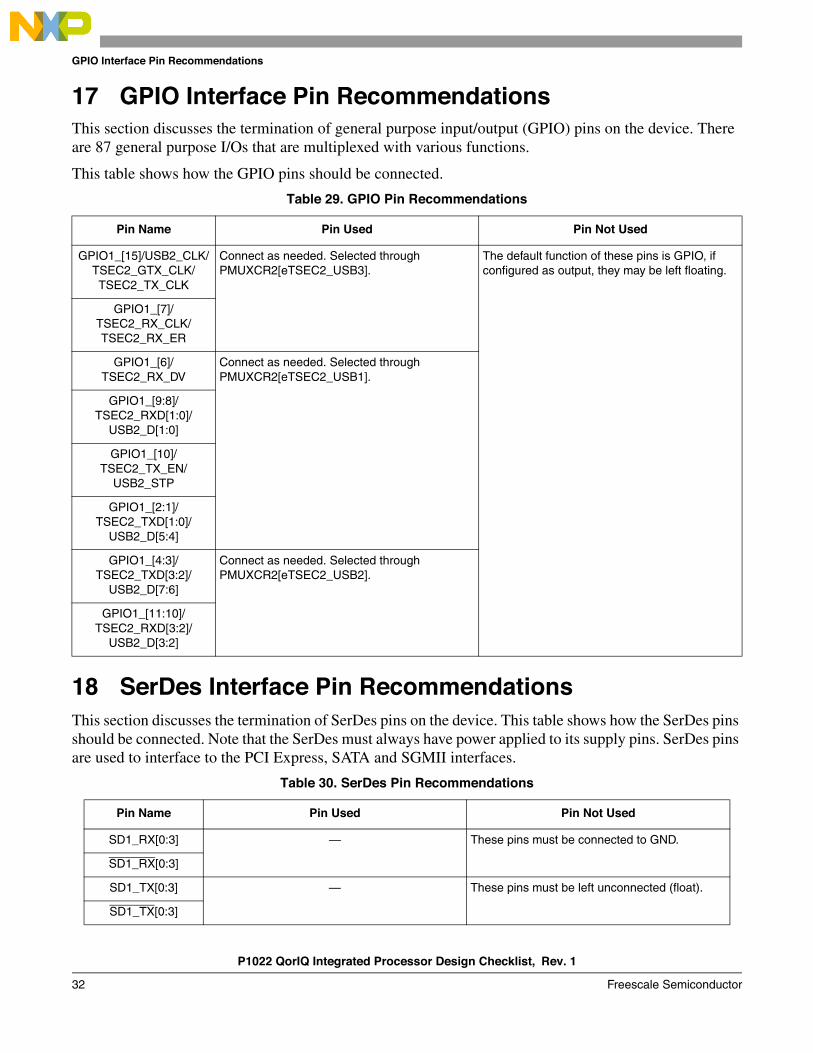
17 GPIO Interface Pin RecommendationsThis section discusses the termination of general purpose input/output (GPIO) pins on the device. There are 87 general purpose I/Os that are multiplexed with various functions.
This table shows how the GPIO pins should be connected.
18 SerDes Interface Pin Recommendations
This section discusses the termination of SerDes pins on the device. This table shows how the SerDes pins should be connected. Note that the SerDes must always have power applied to its supply pins. SerDes pins are used to interface to the PCI Express, SATA and SGMII interfaces.
Table 29. GPIO Pin Recommendations
Pin Name Pin Used Pin Not Used
GPIO1_[15]/USB2_CLK/ TSEC2_GTX_CLK/TSEC2_TX_CLK
Connect as needed. Selected through PMUXCR2[eTSEC2_USB3].
The default function of these pins is GPIO, if configured as output, they may be left floating.
GPIO1_[7]/ TSEC2_RX_CLK/ TSEC2_RX_ER
GPIO1_[6]/ TSEC2_RX_DV
Connect as needed. Selected through PMUXCR2[eTSEC2_USB1].
GPIO1_[9:8]/ TSEC2_RXD[1:0]/
USB2_D[1:0]
GPIO1_[10]/ TSEC2_TX_EN/
USB2_STP
GPIO1_[2:1]/ TSEC2_TXD[1:0]/
USB2_D[5:4]
GPIO1_[4:3]/TSEC2_TXD[3:2]/
USB2_D[7:6]
Connect as needed. Selected through PMUXCR2[eTSEC2_USB2].
GPIO1_[11:10]/ TSEC2_RXD[3:2]/
USB2_D[3:2]
Table 30. SerDes Pin Recommendations
Pin Name Pin Used Pin Not Used
SD1_RX[0:3] — These pins must be connected to GND.
SD1_RX[0:3]
SD1_TX[0:3] — These pins must be left unconnected (float).
SD1_TX[0:3]
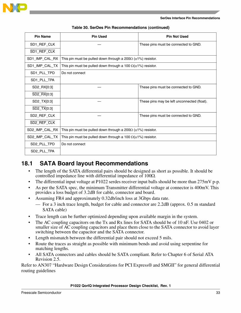
P1022 QorIQ Integrated Processor Design Checklist, Rev. 1
Freescale Semiconductor 33
SerDes Interface Pin Recommendations
18.1 SATA Board layout Recommendations• The length of the SATA differential pairs should be designed as short as possible. It should be
controlled impedance line with differential impedance of 100.• The differential input voltage at P1022 serdes receiver input balls should be more than 275mV p-p.• As per the SATA spec, the minimum Transmitter differential voltage at connector is 400mV. This
provides a loss budget of 3.2dB for cable, connector and board.• Assuming FR4 and approximately 0.32db/inch loss at 3Gbps data rate.
— For a 3 inch trace length, budget for cable and connector are 2.2dB (approx. 0.5 m standard SATA cable)
• Trace length can be further optimized depending upon available margin in the system. • The AC coupling capacitors on the Tx and Rx lines for SATA should be of 10 nF. Use 0402 or
smaller size of AC coupling capacitors and place them close to the SATA connector to avoid layer switching between the capacitor and the SATA connector.
• Length mismatch between the differential pair should not exceed 5 mils. • Route the traces as straight as possible with minimum bends and avoid using serpentine for
matching lengths. • All SATA connectors and cables should be SATA compliant. Refer to Chapter 6 of Serial ATA
Revision 2.5.Refer to AN307 “Hardware Design Considerations for PCI Express® and SMGII” for general differentialrouting guidelines
SD1_REF_CLK — These pins must be connected to GND.
SD1_REF_CLK
SD1_IMP_CAL_RX This pin must be pulled down through a 200 (±1%) resistor.
SD1_IMP_CAL_TX This pin must be pulled down through a 100 (±1%) resistor.
SD1_PLL_TPD Do not connect
SD1_PLL_TPA
SD2_RX[0:3] — These pins must be connected to GND.
SD2_RX[0:3]
SD2_TX[0:3] — These pins may be left unconnected (float).
SD2_TX[0:3]
SD2_REF_CLK — These pins must be connected to GND.
SD2_REF_CLK
SD2_IMP_CAL_RX This pin must be pulled down through a 200 (±1%) resistor.
SD2_IMP_CAL_TX This pin must be pulled down through a 100 (±1%) resistor.
SD2_PLL_TPD Do not connect
SD2_PLL_TPA
Table 30. SerDes Pin Recommendations (continued)
Pin Name Pin Used Pin Not Used
P1022 QorIQ Integrated Processor Design Checklist, Rev. 1
34 Freescale Semiconductor
eTSEC IEEE 1588 Pin Recommendations
19 eTSEC IEEE 1588 Pin Recommendations
This section discusses the termination of eTSEC IEEE 1588 pins on the device. This table shows how the pins should be connected.
20 System Control Pin Recommendations
This section discusses the termination of system control pins on the device. This table shows how the system control pins should be connected.
Note: If on-board programming of NAND boot flash, SPI boot flash or SD card is needed, then an option should be kept (may be via a jumper) to keep HRESET and HRESET_REQ disconnected from each other. Booting from a blank NAND flash or SPI flash causes boot error which in turn causes assertion of HRESET_REQ. When HRESET_REQ is connected with HRESET, then device goes in a recurring reset loop and does not provide enough time for JTAG to take control of the device and perform any operation.
Table 31. eTSEC IEEE 1588 Pin Recommendations
Pin Name Pin Used Pin Not Used
TSEC_1588_CLK_IN/ GPIO1_[12]/USB1_PWRFAULT
External timer reference clock input Configure these pins as GPIO output and leave them unconnected.
TSEC_1588_TRIG_IN1/ GPIO1_[13]/USB2_PWRFAULT
—
TSEC_1588_ALARM_OUT1/ GPO1_[14]
This pin is a reset configuration pin. It has a weak internal pull-up that is enabled only when the processor is in the reset state.
If the POR default is acceptable, this output pin may be left floating.
TSEC_1588_CLK_OUT/ GPO1_[15]
This pin must NOT be pulled down during power-on reset.
TSEC_1588_PULSE_OUT1/ GPO1_[16]
This pin is a reset configuration pin that sets the DDR PLL ratio. These pins require 4.7-k pull-up or pull-down resistors. See Section 6.1.5, “DDR/DDRCLK PLL Ratio.”
Table 32. System Control Pin Recommendations
Pin Name Pin Used Pin Not Used
CKSTP_IN0 Pull high through a 2–10 k resistor to OVDD. Connect to Pin8 of the COP connector (refer to Figure 4).
Pull high through a 2–10 k resistor to OVDD.
CKSTP_IN1
CKSTP_OUT0 Pull this open-drain signal high through a 2–10 k resistor to OVDD. Connect to Pin15 of the COP connector (see Figure 4).This pin is a reset configuration pin. It has a weak internal pull-up that is enabled only when the processor is in the reset state.
If the POR default is acceptable, this output pin may be left floating.
CKSTP_OUT1
HRESET Pull high through a 2–10 k resistor to OVDD2. Connect to Pin13 of the COP connector (refer to Figure 4).
HRESET_REQ Pull high through a 2–10 k resistor to OVDD2. This pin must NOT be pulled down during power-on reset.
This pin must NOT be pulled down during power-on reset.
SRESET Pull high through a 2–10 k resistor to OVDD. Connect to Pin11 of the COP connector
Pull high through a 2–10 k resistor to OVDD.
P1022 QorIQ Integrated Processor Design Checklist, Rev. 1
Freescale Semiconductor 35
Reserved POR Configuration Pins
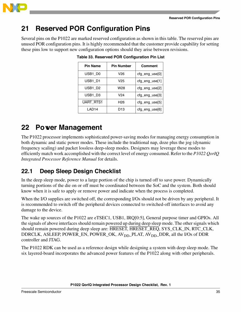
21 Reserved POR Configuration Pins
Several pins on the P1022 are marked reserved configuration as shown in this table. The reserved pins are unused POR configuration pins. It is highly recommended that the customer provide capability for setting these pins low to support new configuration options should they arise between revisions.
22 Power ManagementThe P1022 processor implements sophisticated power-saving modes for managing energy consumption in both dynamic and static power modes. These include the traditional nap, doze plus the jog (dynamic frequency scaling) and packet lossless deep-sleep modes. Designers may leverage these modes to efficiently match work accomplished with the correct level of energy consumed. Refer to the P1022 QorIQ Integrated Processor Reference Manual for details.
22.1 Deep Sleep Design Checklist
In the deep sleep mode, power to a large portion of the chip is turned off to save power. Dynamically turning portions of the die on or off must be coordinated between the SoC and the system. Both should know when it is safe to apply or remove power and indicate when the process is completed.
When the I/O supplies are switched off, the corresponding I/Os should not be driven by any peripheral. It is recommended to switch off the peripheral devices connected to switched-off interfaces to avoid any damage to the device.
The wake up sources of the P1022 are eTSEC1, USB1, IRQ[0:5], General purpose timer and GPIOs. All the signals of above interfaces should remain powered up during deep sleep mode. The other signals which should remain powered during deep sleep are: HRESET, HRESET_REQ, SYS_CLK_IN, RTC_CLK, DDRCLK, ASLEEP, POWER_EN, POWER_OK, AVDD_PLAT, AVDD_DDR, all the I/Os of DDR controller and JTAG.
The P1022 RDK can be used as a reference design while designing a system with deep sleep mode. The six layered-board incorporates the advanced power features of the P1022 along with other peripherals.
Table 33. Reserved POR Configuration Pin List
Pin Name Pin Number Comment
USB1_D0 V26 cfg_eng_use[0]
USB1_D1 V25 cfg_eng_use[1]
USB1_D2 W28 cfg_eng_use[2]
USB1_D3 V24 cfg_eng_use[3]
UART_RTS1 H26 cfg_eng_use[5]
LAD14 D13 cfg_eng_use[6]

P1022 QorIQ Integrated Processor Design Checklist, Rev. 1
36 Freescale Semiconductor
Power and Ground Signals
This table shows how the Power Management control pins should be connected.
23 Power and Ground SignalsThe P1022 has several power supplies and ground signals. When implementing deep sleep mode the switchable supplies and the Always ON supplies need to be separated.
Table 34. Deep Sleep Checklist for Designer
ItemCustomer Comments
Completed
1. Requirements of External Power supply, refer to the P1022 QorIQ Integrated Processor Reference Manual.
2. Power sequencing for deep sleep mode, refer to the P1022 QorIQ Integrated Processor Hardware Specifications.
3. Inputs to the switched off I/O of the P1022 should not be driven.
4. All the pull up resistors should be connected to respective power supplies. Refer to the P1022 QorIQ Integrated Processor Hardware Specifications.
5. If SerDes is enabled, the respective clock inputs should not toggle in deep sleep state.
6. Power regulator is effective across the entire range from maximum power consumption to deep sleep power consumption.
7. Power supply to the wake up sources is separated from the switchable supply.
8. VDDC and VDD are supplied by the same power source. Ensure switching events do not trigger transient voltages, nor trip voltage monitors.
Table 35. Power Management Control Signals
Pin Name Pin used Pin not used
POWER_EN Directly connect to external power switch device. Negation of this signal indicates to the external power regulator to toggle the power switch to off mode
It may be left floating if unconnected.
POWER_OK Directly connect to external power switch device. If there is no external source of POWER_OK, then the POWER_OK has to be tied to logic 1 on the board. In this case POWER_OK will always be asserted to the power management controller (PMC) and the software has to program the counter (PMRCCR[VRCNT]) to a large enough value, which will account for the voltage ramp time for power to become stable. If the e500 PLL is enabled before the power is stable it might become unpredictable and might not lock.
Pull high.
ASLEEP This pin is a reset configuration pin that sets the eLBC ECC enable. This pin requires 4.7-k pull-up or pull-down resistors.This may need to be driven high (that is, by a PLD) if the device to which it is connected does not release this pin to high impedance during reset.
This pin has an internal pull-up enabled only at reset, it may be left floating if unconnected.
Table 36. Power and Ground Pin Recommendations
Pin Comment Power Domain
AVDD_CORE0 Power supply for e500 Core 0 PLL. (VDD through a filter) Switchable
AVDD_CORE1 Power supply for e500 Core 1 PLL. (VDD through a filter) Switchable
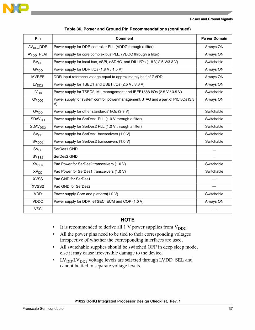
P1022 QorIQ Integrated Processor Design Checklist, Rev. 1
Freescale Semiconductor 37
Power and Ground Signals
NOTE
• It is recommended to derive all 1 V power supplies from VDDC.
• All the power pins need to be tied to their corresponding voltages irrespective of whether the corresponding interfaces are used.
• All switchable supplies should be switched OFF in deep sleep mode, else it may cause irreversible damage to the device.
• LVDD/LVDD2 voltage levels are selected through LVDD_SEL and cannot be tied to separate voltage levels.
AVDD_DDR Power supply for DDR controller PLL (VDDC through a filter) Always ON
AVDD_PLAT Power supply for core complex bus PLL. (VDDC through a filter) Always ON
BVDD Power supply for local bus, eSPI, eSDHC, and DIU I/Os (1.8 V, 2.5 V/3.3 V) Switchable
GVDD Power supply for DDR I/Os (1.8 V / 1.5 V) Always ON
MVREF DDR input reference voltage equal to approximately half of GVDD Always ON
LVDD2 Power supply for TSEC1 and USB1 I/Os (2.5 V / 3.3 V) Always ON
LVDD Power supply for TSEC2, MII management and IEEE1588 I/Os (2.5 V / 3.5 V) Switchable
OVDD2 Power supply for system control, power management, JTAG and a part of PIC I/Os (3.3 V)
Always ON
OVDD Power supply for other standards’ I/Os (3.3 V) Switchable
SDAVDD Power supply for SerDes1 PLL (1.0 V through a filter) Switchable
SDAVDD2 Power supply for SerDes2 PLL (1.0 V through a filter) Switchable
SVDD Power supply for SerDes1 transceivers (1.0 V) Switchable
SVDD2 Power supply for SerDes2 transceivers (1.0 V) Switchable
SVSS SerDes1 GND —
SVSS2 SerDes2 GND —
XVDD2 Pad Power for SerDes2 transceivers (1.0 V) Switchable
XVDD Pad Power for SerDes1 transceivers (1.0 V) Switchable
XVSS Pad GND for SerDes1 —
XVSS2 Pad GND for SerDes2 —
VDD Power supply Core and platform(1.0 V) Switchable
VDDC Power supply for DDR, eTSEC, ECM and COP (1.0 V) Always ON
VSS — —
Table 36. Power and Ground Pin Recommendations (continued)
Pin Comment Power Domain
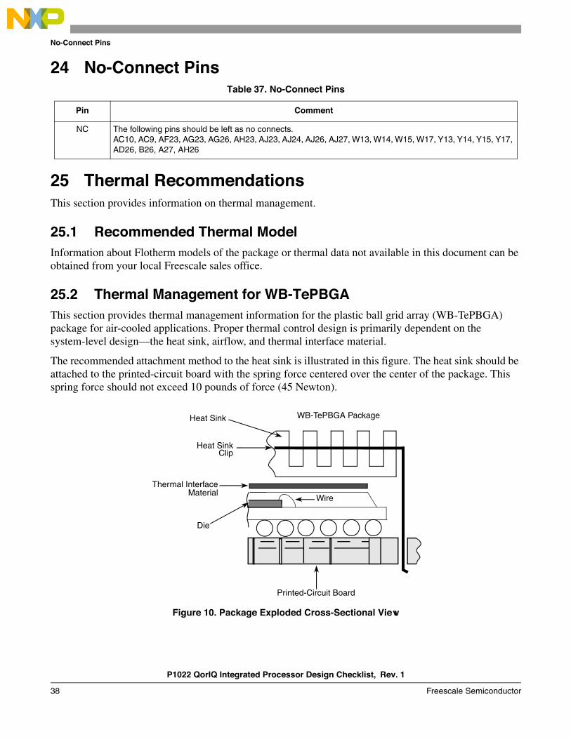
P1022 QorIQ Integrated Processor Design Checklist, Rev. 1
38 Freescale Semiconductor
No-Connect Pins
24 No-Connect Pins
25 Thermal RecommendationsThis section provides information on thermal management.
25.1 Recommended Thermal Model
Information about Flotherm models of the package or thermal data not available in this document can be obtained from your local Freescale sales office.
25.2 Thermal Management for WB-TePBGA
This section provides thermal management information for the plastic ball grid array (WB-TePBGA) package for air-cooled applications. Proper thermal control design is primarily dependent on the system-level design—the heat sink, airflow, and thermal interface material.
The recommended attachment method to the heat sink is illustrated in this figure. The heat sink should be attached to the printed-circuit board with the spring force centered over the center of the package. This spring force should not exceed 10 pounds of force (45 Newton).
Figure 10. Package Exploded Cross-Sectional View
Table 37. No-Connect Pins
Pin Comment
NC The following pins should be left as no connects. AC10, AC9, AF23, AG23, AG26, AH23, AJ23, AJ24, AJ26, AJ27, W13, W14, W15, W17, Y13, Y14, Y15, Y17, AD26, B26, A27, AH26
Thermal Interface
Heat Sink WB-TePBGA Package
Heat SinkClip
Printed-Circuit Board
Material
Die
Wire
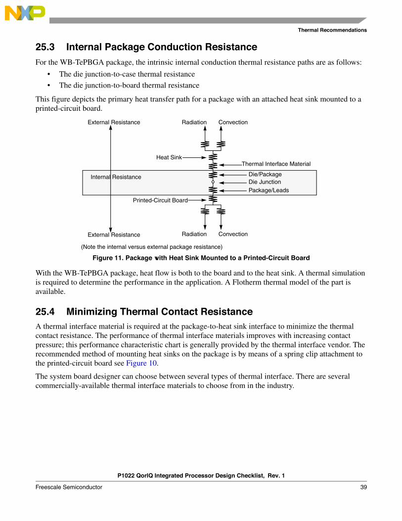
P1022 QorIQ Integrated Processor Design Checklist, Rev. 1
Freescale Semiconductor 39
Thermal Recommendations
25.3 Internal Package Conduction Resistance
For the WB-TePBGA package, the intrinsic internal conduction thermal resistance paths are as follows:
• The die junction-to-case thermal resistance
• The die junction-to-board thermal resistance
This figure depicts the primary heat transfer path for a package with an attached heat sink mounted to a printed-circuit board.
Figure 11. Package with Heat Sink Mounted to a Printed-Circuit Board
With the WB-TePBGA package, heat flow is both to the board and to the heat sink. A thermal simulation is required to determine the performance in the application. A Flotherm thermal model of the part is available.
25.4 Minimizing Thermal Contact Resistance
A thermal interface material is required at the package-to-heat sink interface to minimize the thermal contact resistance. The performance of thermal interface materials improves with increasing contact pressure; this performance characteristic chart is generally provided by the thermal interface vendor. The recommended method of mounting heat sinks on the package is by means of a spring clip attachment to the printed-circuit board see Figure 10.
The system board designer can choose between several types of thermal interface. There are several commercially-available thermal interface materials to choose from in the industry.
External Resistance
External Resistance
Internal Resistance
Radiation Convection
Radiation Convection
Heat Sink
Printed-Circuit Board
Thermal Interface Material
Package/LeadsDie JunctionDie/Package
(Note the internal versus external package resistance)
P1022 QorIQ Integrated Processor Design Checklist, Rev. 1
40 Freescale Semiconductor
Revision History
26 Revision History
This table summarizes the revision history for this document.
Table 38. Document Revision History
Rev.Number
Date Substantive Change(s)
1 05/2014 • In Table 4, changed the sentence in comments column from “Default: Platform speed is at or above 266 MHz.“ to “Default: Platform speed is at or above 300 MHz.“
• In Table 4, changed the sentence in comments column from “Default: Core 0 clock frequency is greater than 450 MHz.“ to “Default: Core 0 clock frequency is greater than or equal to 500 MHz.“
• In Table 4, changed the sentence in comments column from “Default: Core 1 clock frequency is greater than 450 MHz.“ to “Default: Core 1 clock frequency is greater than or equal to 500 MHz.“
• In Table 4, changed the sentence in comments column from “Default: DDR controller clock frequency is greater than or equal to 450 MHz data rate.“ to “Default: DDR controller clock frequency is greater than or equal to 500 MHz data rate.“
• In Table 4, updated functional pins of General-Purpose POR configuration type. • In Table 28, updated the note. • In Table 21, "Pin Used" column for “SDHC_CLK” signal is updated with “33 serial resistor must
be provided for SD_CLK and placed close to P1022 device.” • In Section 3.1, “Configuration and Timing, changed “8 SYSCLK cycles......” to “5 SYSCLK
cycles....”. • In Table 9, added a new row for LCLK[0:1]. • In Table 28, updated PIC pin recommendations for MCP[0:1]/ GPIO3_[14:15], and UDE[0:1]/
GPIO3_[16:17] • Updated notes of Table 28. • Added a note after Table 32. • Added AH26 in comment column of Table 37.
0 10/2011 Initial release
Document Number: AN4343Rev. 105/2014
Information in this document is provided solely to enable system and software
implementers to use Freescale Semiconductor products. There are no express or
implied copyright licenses granted hereunder to design or fabricate any integrated
circuits or integrated circuits based on the information in this document.
Freescale Semiconductor reserves the right to make changes without further notice to
any products herein.
Freescale Semiconductor makes no warranty, representation or guarantee regarding
the suitability of its products for any particular purpose, nor does Freescale
Semiconductor assume any liability arising out of the application or use of any product
or circuit, and specifically disclaims any and all liability, including without limitation
consequential or incidental damages. “Typical” parameters which may be provided in
Freescale Semiconductor data sheets and/or specifications can and do vary in different
applications and actual performance may vary over time. All operating parameters,
including “Typicals” must be validated for each customer application by customer’s
technical experts. Freescale Semiconductor does not convey any license under its
patent rights nor the rights of others. Freescale sells products purusant to standard
terms and conditions of sale, which can be found at the following address:
freescale.com/SalesTermsandConditions .
How to Reach Us:
Home Page: www.freescale.com
Web Support: http://www.freescale.com/support
Freescale, the Freescale logo, PowerQUICC, and QorIQ are trademarks of Freescale Semiconductor, Inc., Reg. U.S. Pat. & Tm. Off. All other product or service names are the property of their respective owners. The Power Architecture and Power.org word marks and the Power and Power.org logos and related marks are trademarks and service marks licensed by Power.org. © 2011, 2014 Freescale Semiconductor, Inc.


![Approval Report Proposal P1022 Primary Production ...€¦ · i 16 December 2014 [26–14] Approval Report – Proposal P1022 Primary Production & Processing Requirements for Raw](https://img.pdfslide.us/doc/110x75/5ba3365109d3f2d14d8d921e/approval-report-proposal-p1022-primary-production-i-16-december-2014-2614.jpg)