Embed Size (px)
Citation preview
AN32181B
Page 1 of 65
Product Standards
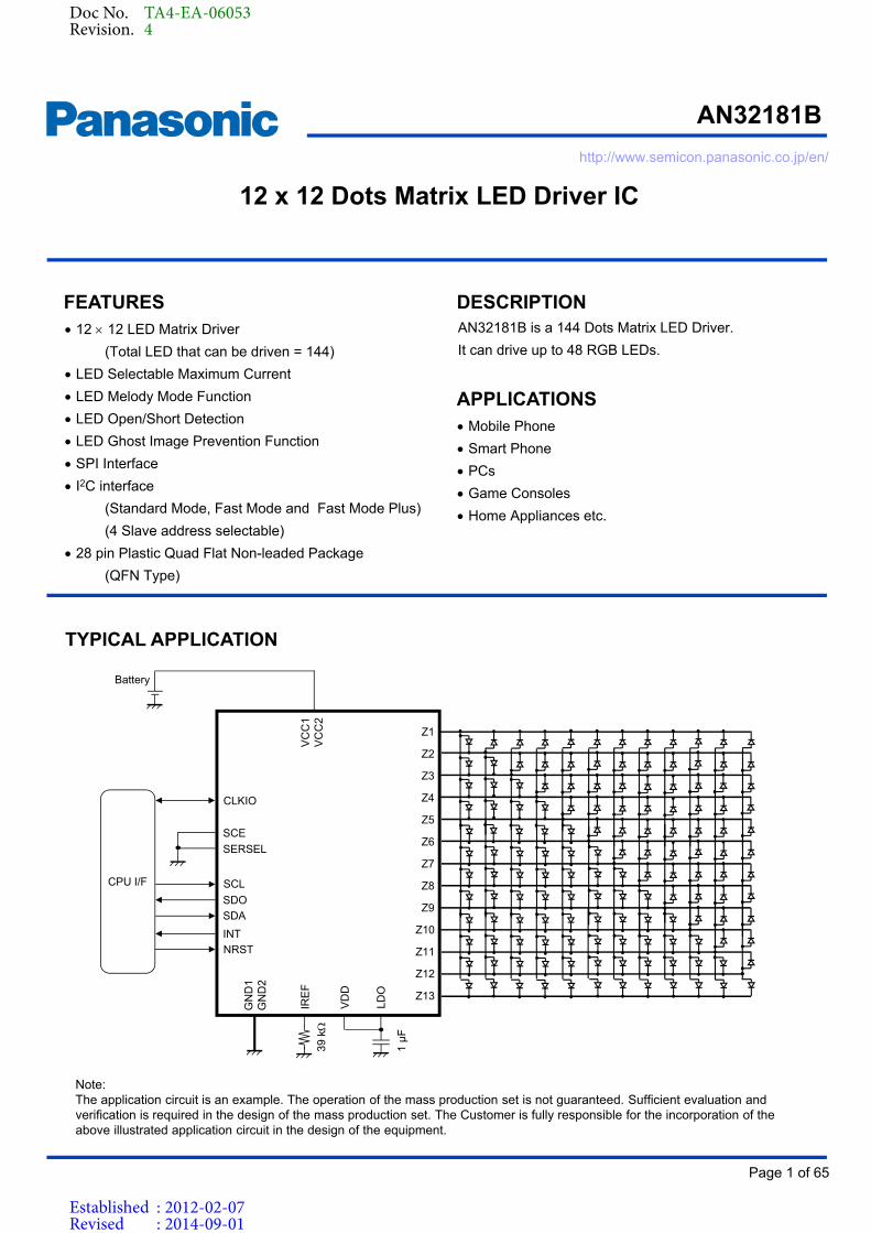
FEATURES DESCRIPTIONAN32181B is a 144 Dots Matrix LED Driver.
It can drive up to 48 RGB LEDs.
12 12 LED Matrix Driver
(Total LED that can be driven = 144)
LED Selectable Maximum Current
LED Melody Mode Function
LED Open/Short Detection
LED Ghost Image Prevention Function
SPI Interface
I2C interface
(Standard Mode, Fast Mode and Fast Mode Plus)
(4 Slave address selectable)
28 pin Plastic Quad Flat Non-leaded Package
(QFN Type)
APPLICATIONS
12 x 12 Dots Matrix LED Driver IC
http://www.semicon.panasonic.co.jp/en/
Mobile Phone
Smart Phone
PCs
Game Consoles
Home Appliances etc.
TYPICAL APPLICATION
VC
C1
VC
C2
Battery
GN
D1
GN
D2
SDA
NRST
SCL
IRE
F
CLKIO
LDO
CPU I/F
VD
D
Z4
Z3
Z5
Z1
Z2
Z9
Z8
Z10
Z6
Z7
Z12
Z11
Z13
SERSEL
INT
SDO
SCE
39 k
1 µ
F
Note:The application circuit is an example. The operation of the mass production set is not guaranteed. Sufficient evaluation and verification is required in the design of the mass production set. The Customer is fully responsible for the incorporation of the above illustrated application circuit in the design of the equipment.
Doc No. TA4-EA-06053Revision. 4
Established : 2012-02-07Revised : 2014-09-01
AN32181B
Page 2 of 65
Product Standards
CONTENTS
FEATURES ………………………………………………………………………………… 1
DESCRIPTION ……..……………………………………………………………………… 1
APPLICATIONS …………………………………………………………………………… 1
TYPICAL APPLICATION ………………………………………………………………… 1
CONTENTS ………………………………………………………………………………… 2
ABSOLUTE MAXIMUM RATINGS ……………………………………………………… 3
POWER DISSIPATION RATING ………………………………………………………… 3
RECOMMENDED OPERATING CONDITIONS ……………………………………….. 4
ELECTRICAL CHARACTERISTICS .…………………………………………………… 5
PIN CONFIGURATION ……………………………………………………………………13
PIN FUNCTIONS ..…………………………………………………………………………13
FUNCTIONAL BLOCK DIAGRAM ………………………………………………………15
OPERATION ….…………………………………………………………………………….16
PACKAGE INFORMATION ………………………………………………………………64
IMPORTANT NOTICE .…………………………………………………………………… 65
Doc No. TA4-EA-06053Revision. 4
Established : 2012-02-07Revised : 2014-09-01

AN32181B
Page 3 of 65
Product Standards
ABSOLUTE MAXIMUM RATINGS
Parameter Symbol Rating Unit Note
Supply voltageVCCMAX 6.0 V *1
VDDMAX 6.0 V *1
Operating ambience temperature Topr – 30 to + 85 C *2
Operating junction temperature Tj – 30 to + 125 C *2
Storage temperature Tstg – 55 to + 125 C *2
Input Voltage RangeVSERSEL, VSCL, VSDA,
VSCE, VCLKIO, VNRST
– 0.3 to 6.0 V —
Output Voltage Range
VINT, VCLKIO, VSDO,
VZ1, VZ2, VZ3, VZ4, VZ5, VZ6, VZ7,
VZ8, VZ9, VZ10, VZ11, VZ12, VZ13
– 0.3 to 6.0 V —
VLDO – 0.3 to 4.0 V —
ESD HBM 2.0 kV —
POWER DISSIPATION RATING
Package j-a PD (Ta = 25 C) PD (Ta = 85 C)
28 pin Plastic Quad Flat Non-leaded package (QFN Type) 175.5 C / W 0.569 W 0.228 W
CAUTIONAlthough this IC has built-in ESD protection circuit, it may still sustain permanent damage if not handledproperly. Therefore, proper ESD precautions are recommended to avoid electrostatic damage to the MOS gates
ORDERING INFORMATION
Order Number Feature Package Output Supply
AN32181B-VB Matrix LED Driver 28 pin QFN Emboss Taping
Note: This product may sustain permanent damage if subjected to conditions higher than the above stated absolute maximum
rating. This rating is the maximum rating and device operating at this range is not guaranteed as it is higher than our stated
recommended operating range. When subjected under the absolute maximum rating for a long time, the reliability of the
product may be affected.
VCCMAX is voltage for VCC1 and VCC2. VCC1 = VCC2.
VDDMAX is voltage for VDD.
Do not apply external currents or voltages to any pin not specifically mentioned.
*1: The values under the condition not exceeding the above absolute maximum ratings and the power dissipation.
*2: Except for operating ambient temperature, operating junction temperature and storage temperature,
all ratings are for Ta = 25C.
Note: For the actual usage, please refer to the PD-Ta characteristics diagram in the Package Standards, follow the power supply
voltage, load and ambient temperature conditions to ensure that there is enough margin and the thermal design does
not exceed the allowable value.
Doc No. TA4-EA-06053Revision. 4
Established : 2012-02-07Revised : 2014-09-01
AN32181B
Page 4 of 65
Product Standards
RECOMMENDED OPERATING CONDITIONS
Parameter Symbol Min Typ Max Unit Note
Supply voltage rangeVCC 3.1 3.6 5.5 V *1
VDD 1.70 1.85 5.50 V *1
Input Voltage Range
VSCL, VSDA,
VSCE, VCLKIO
– 0.3 — VDD + 0.3 V *2
VSERSEL, VNRST – 0.3 — VCC + 0.3 V *2
Output Voltage Range
VINT, VCLKIO, VSDO – 0.3 — VDD + 0.3 V *2
VZ1, VZ2, VZ3, VZ4, VZ5, VZ6, VZ7,
VZ8, VZ9, VZ10, VZ11, VZ12, VZ13
– 0.3 — VCC + 0.3 V *2
VLDO – 0.3 — 3.5 V —
Note: *1: The values under the condition not exceeding the above absolute maximum ratings and the power dissipation.
Do not apply external currents and voltages to any pin not specifically mentioned.
Voltage values, unless otherwise specified, are with respect to GND. GND is voltage for GND1 and GND2.
GND1 = GND2.
VCC is voltage for VCC1 and VCC2. VCC1 = VCC2.
VDD is voltage for VDD.
Do not apply external currents or voltages to any pin not specifically mentioned.
*2: (VCC + 0.3 ) V must not exceed 6.0 V. (VDD + 0.3) V must not exceed 6.0 V.
Doc No. TA4-EA-06053Revision. 4
Established : 2012-02-07Revised : 2014-09-01
AN32181B
Page 5 of 65
Product Standards
Parameter Symbol Condition Limits
Unit NoteMin Typ Max
Circuit Current
Circuit Current (1)
OFF ModeICC1 VNRST = 0 V — 0 1 µA —
Circuit Current (2)
OFF ModeICC2 VNRST = High — 240 500 µA —
Internal Oscillator
Oscillation Frequency FDC1 — 1.92 2.40 2.88 MHz —
SCAN Switch
Switch On Resistance RSCAN IZ1 to Z12 = – 20 mA — 1.0 2.5 —
Constant Voltage Source (LDO)
Output voltage (1) VL1 ILDO = – 10 µA 2.75 2.85 2.95 V —
Output voltage (2) VL2 ILDO = – 15 mA 2.75 2.85 2.95 V —
CLKIO
High Level Input Voltage Range VIH1
High Level Acknowledged Voltage (At External CLK Input Mode)
0.7 VDD
—VDD
+ 0.3V —
Low Level Input Voltage Range VIL1
Low Level Acknowledged Voltage (At External CLK Input Mode)
– 0.3 —0.3 VDD
V —
High Level Output Voltage VOH1
ICLKIO = – 1 mA
(At Internal CLK Output Mode)0.8 VDD
—VDD
+ 0.3V —
Low Level Output Voltage VOL1
ICLKIO = 1 mA
(At Internal CLK Output Mode)– 0.3 —
0.2 VDD
V —
High Level input Current IIH1
VCC = 5.5 V, VDD = 5.5 V
VCLKIO = 5.5 V– 1 0 1 µA —
Low Level input Current IIL1
VCC = 5.5 V, VDD = 5.5 V
VCLKIO = 0 V– 1 0 1 µA —
ELECTRICAL CHARACTERISTICSVCC = 3.6 V, VDD = 1.85 V
Note: Operating Ambient Temperature, Ta = 25 C 2 C, unless specifically mentioned
Doc No. TA4-EA-06053Revision. 4
Established : 2012-02-07Revised : 2014-09-01
AN32181B
Page 6 of 65
Product Standards
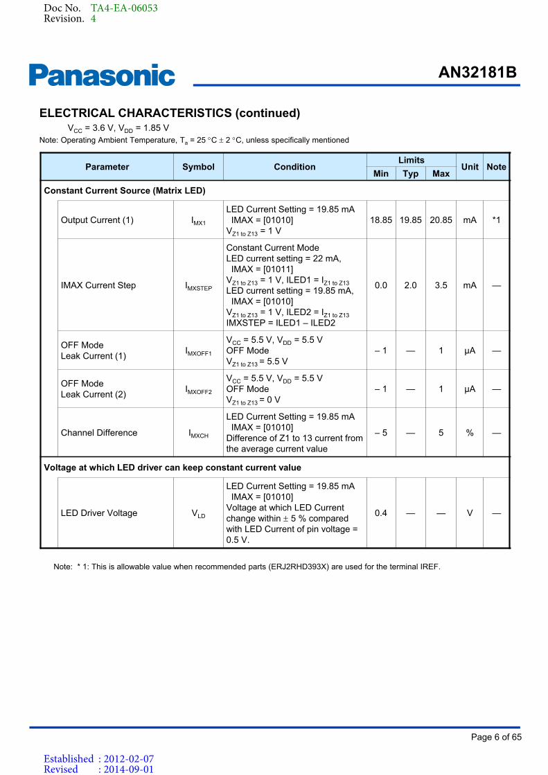
Parameter Symbol Condition Limits
Unit NoteMin Typ Max
Constant Current Source (Matrix LED)
Output Current (1) IMX1
LED Current Setting = 19.85 mAIMAX = [01010]
VZ1 to Z13 = 1 V18.85 19.85 20.85 mA *1
IMAX Current Step IMXSTEP
Constant Current ModeLED current setting = 22 mA,
IMAX = [01011]VZ1 to Z13 = 1 V, ILED1 = IZ1 to Z13
LED current setting = 19.85 mA, IMAX = [01010]
VZ1 to Z13 = 1 V, ILED2 = IZ1 to Z13
IMXSTEP = ILED1 – ILED2
0.0 2.0 3.5 mA —
OFF ModeLeak Current (1)
IMXOFF1
VCC = 5.5 V, VDD = 5.5 VOFF ModeVZ1 to Z13 = 5.5 V
– 1 — 1 µA —
OFF ModeLeak Current (2)
IMXOFF2
VCC = 5.5 V, VDD = 5.5 VOFF ModeVZ1 to Z13 = 0 V
– 1 — 1 µA —
Channel Difference IMXCH
LED Current Setting = 19.85 mAIMAX = [01010]
Difference of Z1 to 13 current from the average current value
– 5 — 5 % —
Voltage at which LED driver can keep constant current value
LED Driver Voltage VLD
LED Current Setting = 19.85 mAIMAX = [01010]
Voltage at which LED Current change within 5 % compared with LED Current of pin voltage = 0.5 V.
0.4 — — V —
Note: * 1: This is allowable value when recommended parts (ERJ2RHD393X) are used for the terminal IREF.
ELECTRICAL CHARACTERISTICS (continued)VCC = 3.6 V, VDD = 1.85 V
Note: Operating Ambient Temperature, Ta = 25 C 2 C, unless specifically mentioned
Doc No. TA4-EA-06053Revision. 4
Established : 2012-02-07Revised : 2014-09-01
AN32181B
Page 7 of 65
Product Standards
Parameter Symbol Condition Limits
Unit NoteMin Typ Max
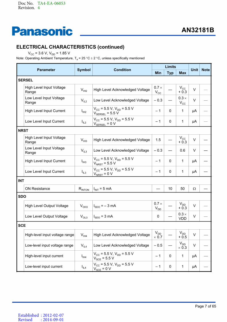
SERSEL
High Level Input Voltage Range
VIH2 High Level Acknowledged Voltage0.7 VCC
—VCC
+ 0.3V —
Low Level Input Voltage Range
VIL2 Low Level Acknowledged Voltage – 0.3 —0.3 VCC
V —
High Level Input Current IIH2VCC = 5.5 V, VDD = 5.5 VVSERSEL = 5.5 V
– 1 0 1 µA —
Low Level Input Current IIL2VCC = 5.5 V, VDD = 5.5 VVSERSEL = 0 V
– 1 0 1 µA —
NRST
High Level Input Voltage Range
VIH3 High Level Acknowledged Voltage 1.5 —VCC
+ 0.3V —
Low Level Input Voltage Range
VIL3 Low Level Acknowledged Voltage – 0.3 — 0.6 V —
High Level Input Current IIH3VCC = 5.5 V, VDD = 5.5 VVNRST = 5.5 V
– 1 0 1 µA —
Low Level Input Current IIL3VCC = 5.5 V, VDD = 5.5 VVNRST = 0 V
– 1 0 1 µA —
INT
ON Resistance RINTON IINT = 5 mA — 10 50 —
SDO
High Level Output Voltage VOH3 ISDO = – 3 mA0.7 VDD
—VDD
+ 0.3V —
Low Level Output Voltage VOL3 ISDO = 3 mA 0 —0.3 VDD
V —
SCE
High-level input voltage range VIH4 High Level Acknowledged VoltageVDD
0.7—
VDD
+ 0.5V
Low-level input voltage range VIL4 Low Level Acknowledged Voltage – 0.5 —VDD
0.3V
High-level input current IIH4VCC = 5.5 V, VDD = 5.5 VVSCE = 5.5 V
– 1 0 1 µA
Low-level input current IIL4VCC = 5.5 V, VDD = 5.5 VVSCE = 0 V
– 1 0 1 µA
ELECTRICAL CHARACTERISTICS (continued)VCC = 3.6 V, VDD = 1.85 V
Note: Operating Ambient Temperature, Ta = 25 C 2 C, unless specifically mentioned
Doc No. TA4-EA-06053Revision. 4
Established : 2012-02-07Revised : 2014-09-01

AN32181B
Page 8 of 65
Product Standards
Parameter Symbol Condition Limits
Unit NoteMin Typ Max
I2C bus (Internal I/O stage characteristics) (SCL, SDA)
Low-level input voltage VILVoltage which recognized that SDA and SCL are Low-level
– 0.5 —0.3 VDD
V *2
High-level input voltage VIHVoltage which recognized that SDA and SCL are High-level
0.7 VDD
—VDDmax
+ 0.5V
*2
*3
Low-level output voltage 1 VOL1
VDD > 2 V
ISDA, ISCL = 3 mA0 — 0.4 V —
Low-level output voltage 2 VOL2
VDD < 2 V
ISDA, ISCL = 3 mA0 —
0.2 VDD
V —
Low-level output current IOL VSDA = 0.4 V 20 — — mA —
Input current each I/O pin Ii
VCC = 5.5 V , VDD = 5.5 V
VSDA, VSCL =
0.1 VDDmax to 0.9 VDDmax
– 10 0 10 µA *3
SCL clock frequency fSCL — 0 — 1000 kHz —
ELECTRICAL CHARACTERISTICS (continued)VCC = 3.6 V, VDD = 1.85 V
Note: Operating Ambient Temperature, Ta = 25 C 2 C, unless specifically mentioned
Note: *2 : The input threshold voltage of I2C bus (Vth) is linked to VDD (I2C bus I/O stage supply voltage).
In case the pull-up voltage is not VDD, the threshold voltage (Vth) is fixed to ((VDD / 2) (Schmitt width) / 2 )
and High-level, Low-level of input voltage are not specified.
In this case, pay attention to Low-level (max.) value (VILmax).
It is recommended that the pull-up voltage of I2C bus is set to the I2C bus I/O stage supply voltage (VDD).
*3 : VDDmax refers to the maximum operating supply voltage of VDD.
Doc No. TA4-EA-06053Revision. 4
Established : 2012-02-07Revised : 2014-09-01
AN32181B
Page 9 of 65
Product Standards
Parameter Symbol Condition Limits
Unit NoteMin Typ Max
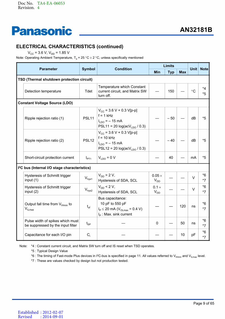
TSD (Thermal shutdown protection circuit)
Detection temperature TdetTemperature which Constant current circuit, and Matrix SW turn off.
— 150 — C*4
*5
Constant Voltage Source (LDO)
Ripple rejection ratio (1) PSL11
VCC = 3.6 V + 0.3 V[p-p]
f = 1 kHz
ILDO = – 15 mA
PSL11 = 20 log(acVLDO / 0.3)
— – 50 — dB *5
Ripple rejection ratio (2) PSL12
VCC = 3.6 V + 0.3 V[p-p]
f = 10 kHz
ILDO = – 15 mA
PSL12 = 20 log(acVLDO / 0.3)
— – 40 — dB *5
Short-circuit protection current IPT1 VLDO = 0 V — 40 — mA *5
I2C bus (Internal I/O stage characteristics)
Hysteresis of Schmitt trigger input (1)
Vhys1
VDD > 2 V,
Hysteresis of SDA, SCL0.05
VDD— — V
*6
*7
Hysteresis of Schmitt trigger input (2)
Vhys2
VDD < 2 V,
Hysteresis of SDA, SCL0.1 VDD
— — V*6
*7
Output fall time from VIHmin to VILmax
tof
Bus capacitance:
10 pF to 550 pF
IP 20 mA (VOLmax = 0.4 V)
IP : Max. sink current
— — 120 ns*6
*7
Pulse width of spikes which must be suppressed by the input filter
tSP — 0 — 50 ns *6
*7
Capacitance for each I/O pin Ci — — — 10 pF*6
*7
Note: *4 : Constant current circuit, and Matrix SW turn off and IS reset when TSD operates.
*5 : Typical Design Value
*6 : The timing of Fast-mode Plus devices in I2C-bus is specified in page 11. All values referred to VIHmin and VILmax level.
*7 : These are values checked by design but not production tested.
ELECTRICAL CHARACTERISTICS (continued)VCC = 3.6 V, VDD = 1.85 V
Note: Operating Ambient Temperature, Ta = 25 C 2 C, unless specifically mentioned
Doc No. TA4-EA-06053Revision. 4
Established : 2012-02-07Revised : 2014-09-01
AN32181B
Page 10 of 65
Product Standards
Parameter Symbol Condition Limits
Unit NoteMin Typ Max
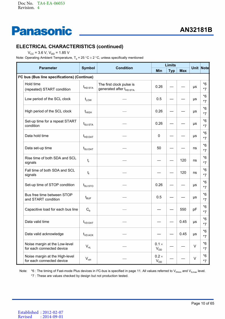
I2C bus (Bus line specifications) (Continue)
Hold time
(repeated) START conditiontHD:STA
The first clock pulse is generated after tHD:STA.
0.26 — — µs*6
*7
Low period of the SCL clock tLOW 0.5 — — µs*6
*7
High period of the SCL clock tHIGH 0.26 — — µs*6
*7
Set-up time for a repeat START condition
tSU:STA 0.26 — — µs*6
*7
Data hold time tHD:DAT 0 — — µs*6
*7
Data set-up time tSU:DAT 50 — — ns*6
*7
Rise time of both SDA and SCL signals
tr — — 120 ns*6
*7
Fall time of both SDA and SCL signals
tf — — 120 ns*6
*7
Set-up time of STOP condition tSU:STO 0.26 — — µs*6
*7
Bus free time between STOP and START condition
tBUF 0.5 — — µs*6
*7
Capacitive load for each bus line Cb — — 550 pF*6
*7
Data valid time tVD:DAT — — 0.45 µs*6
*7
Data valid acknowledge tVD:ACK — — 0.45 µs*6
*7
Noise margin at the Low-level for each connected device
VnL 0.1 VDD
— — V*6
*7
Noise margin at the High-level for each connected device
VnH 0.2 VDD
— — V*6
*7
ELECTRICAL CHARACTERISTICS (continued)VCC = 3.6 V, VDD = 1.85 V
Note: Operating Ambient Temperature, Ta = 25 C 2 C, unless specifically mentioned
Note: *6 : The timing of Fast-mode Plus devices in I2C-bus is specified in page 11. All values referred to VIHmin and VILmax level.
*7 : These are values checked by design but not production tested.
Doc No. TA4-EA-06053Revision. 4
Established : 2012-02-07Revised : 2014-09-01
AN32181B
Page 11 of 65
Product Standards
ELECTRICAL CHARACTERISTICS (continued)VCC = 3.6 V, VDD = 1.85 V
Note: Operating Ambient Temperature, Ta = 25 C 2 C, unless specifically mentioned
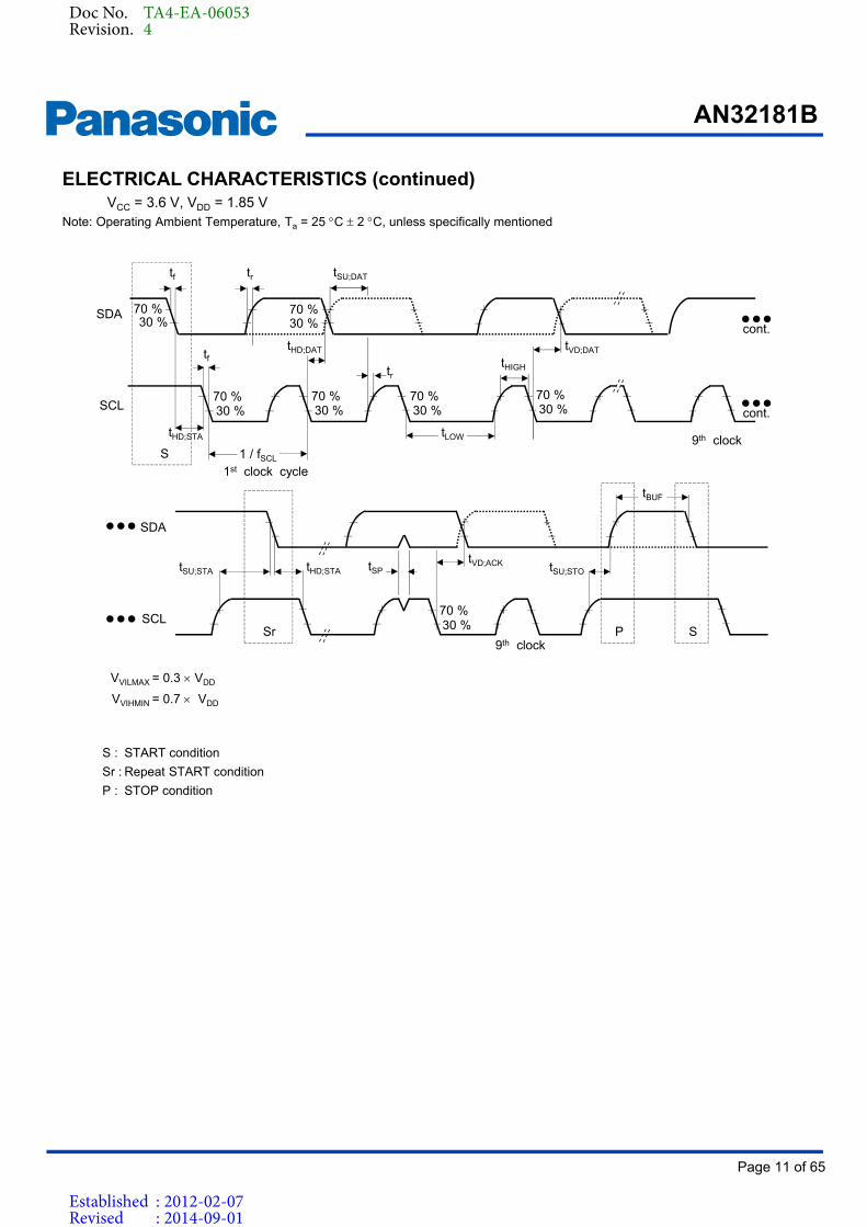
S : START condition
Sr : Repeat START condition
P : STOP condition
tf tr
tf
70 %30 %
SDA
SCL
tHD;STA
70 %30 %
70 %30 %
S 1 / fSCL
1st clock cycle
tHD;DAT
tSU;DAT
70 %30 %
70 %30 %
tr
tLOW
70 %30 %
tHIGH
tVD;DAT
● ● ●
cont.
9th clock
● ● ●
cont.
tHD;STA
Sr
tSP
70 %30 %
tSU;STO
VVILMAX = 0.3 VDD
VVIHMIN = 0.7 VDD
tSU;STA
9th clock
tVD;ACK
tBUF
P S
SDA
SCL
● ● ●
● ● ●
Doc No. TA4-EA-06053Revision. 4
Established : 2012-02-07Revised : 2014-09-01
AN32181B
Page 12 of 65
Product Standards
Parameter Symbol Condition Limits
Unit NoteMin Typ Max
SPI interface characteristics (VDD = 1.85 V 3 %) Reception timing
SCL cycle period tscyc1 — — 200 — ns *5
SCL cycle period High period twhc1 — — 100 — ns *5
SCL cycle period Low period twlc1 — — 100 — ns *5
Serial data setup time tss1 — — 142 — ns *5
Serial data hold time tsh1 — — 142 — ns *5
Transceiving interval tcsw1 — — 100 — ns *5
Chip enable setup time tcss1 — — 5 — ns *5
Chip enable hold time tcgh1 — — 5 — ns *5
SPI interface characteristics (VDD = 1.85 V 3 %) Transmission timing
SCL cycle period tscyc1 — — 200 — ns *5
SCL cycle period High period twhc1 — — 100 — ns *5
SCL cycle period Low period twlc1 — — 100 — ns *5
Serial data setup time tss1 — — 142 — ns *5
Serial data hold time tsh1 — — 142 — ns *5
Transceiving interval tcsw1 — — 100 — ns *5
Chip enable setup time tcss1 — — 5 — ns *5
Chip enable hold time tcgh1 — — 5 — ns *5
DC delay time tdodly1 Read mode only — 30 — ns *5
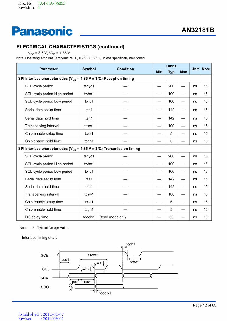
Interface timing chart
twlc1
tscyc1
tsh1tss1
tcss1tcsw1
tcgh1
tdodly1
twhc1SCL
SDA
SCE
SDO
ELECTRICAL CHARACTERISTICS (continued)VCC = 3.6 V, VDD = 1.85 V
Note: Operating Ambient Temperature, Ta = 25 C 2 C, unless specifically mentioned
Note: *5 : Typical Design Value
Doc No. TA4-EA-06053Revision. 4
Established : 2012-02-07Revised : 2014-09-01
AN32181B
Page 13 of 65
Product Standards
PIN CONFIGURATION
Top View
23
24
25
26
27
28
GND1
LDO
Z3
Z2
Z1
CLKIO
14
13
12
11
10
9
22 21 20 19 18 17 16 15
1 2 3 4 5 6 7 8
GND2
Z10
Z11
Z12
Z13
SERSEL
VC
C1
Z4
Z5
Z6
Z7
Z8
Z9
VC
C2
SC
E
SD
O
SD
A
SC
L
VD
D
INT
IRE
F
NR
ST
PIN FUNCTIONS
Pin No. Pin name Type DescriptionPin processing
at unused
1 SCE Input
Chip enable signal for SPI interface.SERSEL = High
Then GND or VCC
Slave address selection pin for I2C interface.SERSEL = Low
Then GND or VCC
or SCL or SDA
2 SDO Output Data output pin for SPI interface Open
3 SDA Input/Output Data input / output pin for SPI or I2C interface (Required pin)
4 SCL Input Clock input pin for SPI or I2C interface (Required pin)
5 VDD Power Supply Power supply for SPI or I2C interface (Required pin)
6 INT (*1) Output Interruption signal output pin / Open drain Open
7 IREF Output Resistor connection pin for constant current setup (Required pin)
8 NRST Input Reset input pin (Required pin)
9 SERSEL Input Serial Interface selection pin / SPI or I2C interface (Required pin)
10 Z13 OutputConstant current circuit, PWM control output pin,Control switch pin for matrix driver
Open
Note: *1 : INT pin must be pulled up to VDD when it is in use.
Doc No. TA4-EA-06053Revision. 4
Established : 2012-02-07Revised : 2014-09-01
AN32181B
Page 14 of 65
Product Standards
PIN FUNCTIONS (continued)
Pin No. Pin name Type DescriptionPin processing
at unused
11 Z12 OutputConstant current circuit, PWM control output pin,
Control switch pin for matrix driverOpen
12 Z11 OutputConstant current circuit, PWM control output pin,
Control switch pin for matrix driverOpen
13 Z10 OutputConstant current circuit, PWM control output pin,
Control switch pin for matrix driverOpen
14
23
GND2
GND1Ground Ground pin (Required pin)
15
22
VCC2
VCC1Power Supply Power supply for matrix driver, Internal reference circuit
Battery or External power supply
16 Z9 OutputConstant current circuit, PWM control output pin,
Control switch pin for matrix driverOpen
17 Z8 OutputConstant current circuit, PWM control output pin,
Control switch pin for matrix driverOpen
18 Z7 OutputConstant current circuit, PWM control output pin,
Control switch pin for matrix driverOpen
19 Z6 OutputConstant current circuit, PWM control output pin,
Control switch pin for matrix driverOpen
20 Z5 OutputConstant current circuit, PWM control output pin,
Control switch pin for matrix driverOpen
21 Z4 OutputConstant current circuit, PWM control output pin,
Control switch pin for matrix driverOpen
24 LDO Output LDO output pin (Required pin)
25 Z3 OutputConstant current circuit, PWM control output pin,
Control switch pin for matrix driverOpen
26 Z2 OutputConstant current circuit, PWM control output pin,
Control switch pin for matrix driverOpen
27 Z1 OutputConstant current circuit, PWM control output pin,
Control switch pin for matrix driverOpen
28 CLKIO Input/Output Reference clock input/output, LED control input pin Open
Doc No. TA4-EA-06053Revision. 4
Established : 2012-02-07Revised : 2014-09-01
AN32181B
Page 15 of 65
Product Standards
FUNCTIONAL BLOCK DIAGRAM
I2C/ SPI serial interface
frameand brightness
controller
Moving patterngenerator
SC
L
Logic
SD
A
VD
D
Voltageregulators
PWM Step control
Scroll Function
SC
E
SD
O
LDO
Z13
( 1)
( 2)
( 3)
( 4)
( 5)
NR
ST
( 8)
SERSEL( 9)
(10)
GND2(14)
GND1 (23)
(24)
Z11
Z12
Z10
(11)
(12)
(13)
Z4
Z6
Z8
Z7
Z5
Z9
(16)
(17)
(19)
(18)
(20)
(21)
Z2
Z1
Z3 (25)
(27)
(26)
CLKIO
Music Synchronize
Function
Clock Output
(28)
INT
( 6)
(22)
VC
C2
(15)
IRE
F(
7)
Reference Generator
PeriodicalScanningSelectors
&LED
drivers
Periodical Scanning Selectors&
LED drivers
PeriodicalScanningSelectors
&LED
drivers
VC
C1
Notes: This block diagram is for explaining functions. Part of the block diagram may be omitted, or it may be simplified.
Doc No. TA4-EA-06053Revision. 4
Established : 2012-02-07Revised : 2014-09-01
AN32181B
Page 16 of 65
Product Standards
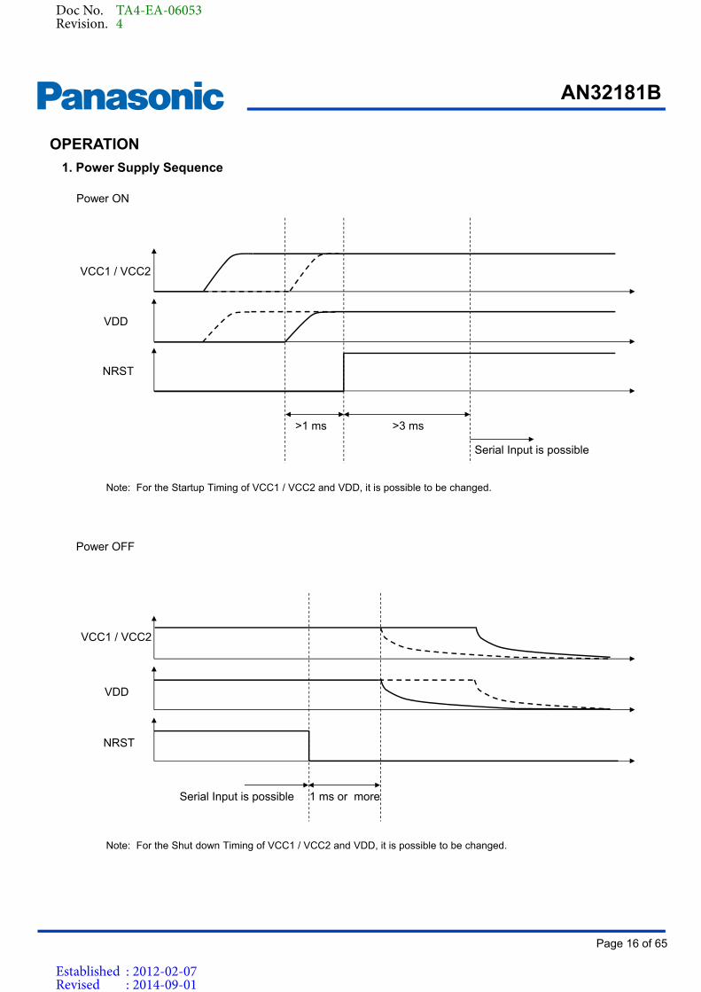
1. Power Supply Sequence
OPERATION
Serial Input is possible
NRST
>1 ms
VCC1 / VCC2
VDD
>3 ms
Note: For the Startup Timing of VCC1 / VCC2 and VDD, it is possible to be changed.
Power ON
NRST
Serial Input is possible
VDD
VCC1 / VCC2
1 ms or more
Note: For the Shut down Timing of VCC1 / VCC2 and VDD, it is possible to be changed.
Power OFF
Doc No. TA4-EA-06053Revision. 4
Established : 2012-02-07Revised : 2014-09-01
AN32181B
Page 17 of 65
Product Standards
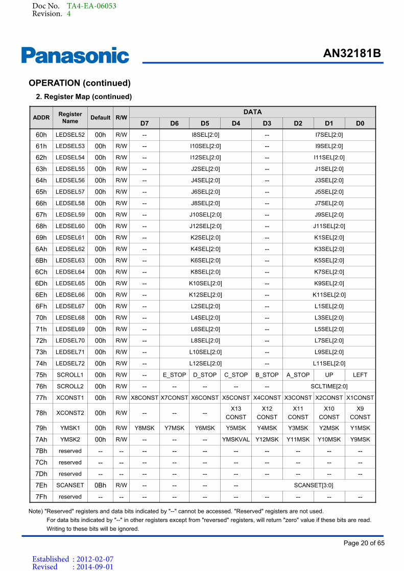
2. Register Map
ADDRRegister
NameDefault R/W
DATA
D7 D6 D5 D4 D3 D2 D1 D0
00h RST 00h R/W -- -- -- -- -- RAM2RST RAM1RST SRST
01h reserved -- -- -- -- -- -- -- -- -- --
02h reserved -- -- -- -- -- -- -- -- -- --
03h CLKCTL 78h R/W IMAX[4:0] OSCEN CLKOUT EXTCLK
04h MTXON 00h R/W -- -- -- -- ZPDEN MTXMODE[1:0] MTXON
05h FRMSEL 00h R/W -- -- -- -- -- -- -- FRMSEL
06h MTXON1 00h R/W A8ON A7ON A6ON A5ON A4ON A3ON A2ON A1ON
07h MTXON2 00h R/W B4ON B3ON B2ON B1ON A12ON A11ON A10ON A9ON
08h MTXON3 00h R/W B12ON B11ON B10ON B9ON B8ON B7ON B6ON B5ON
09h MTXON4 00h R/W C8ON C7ON C6ON C5ON C4ON C3ON C2ON C1ON
0Ah MTXON5 00h R/W D4ON D3ON D2ON D1ON C12ON C11ON C10ON C9ON
0Bh MTXON6 00h R/W D12ON D11ON D10ON D9ON D8ON D7ON D6ON D5ON
0Ch MTXON7 00h R/W E8ON E7ON E6ON E5ON E4ON E3ON E2ON E1ON
0Dh MTXON8 00h R/W F4ON F3ON F2ON F1ON E12ON E11ON E10ON E9ON
0Eh MTXON9 00h R/W F12ON F11ON F10ON F9ON F8ON F7ON F6ON F5ON
0Fh MTXON10 00h R/W G8ON G7ON G6ON G5ON G4ON G3ON G2ON G1ON
10h MTXON11 00h R/W H4ON H3ON H2ON H1ON G12ON G11ON G10ON G9ON
11h MTXON12 00h R/W H12ON H11ON H10ON H9ON H8ON H7ON H6ON H5ON
12h MTXON13 00h R/W I8ON I7ON I6ON I5ON I4ON I3ON I2ON I1ON
13h MTXON14 00h R/W J4ON J3ON J2ON J1ON I12ON I11ON I10ON I9ON
14h MTXON15 00h R/W J12ON J11ON J10ON J9ON J8ON J7ON J6ON J5ON
15h MTXON16 00h R/W K8ON K7ON K6ON K5ON K4ON K3ON K2ON K1ON
16h MTXON17 00h R/W L4ON L3ON L2ON L1ON K12ON K11ON K10ON K9ON
17h MTXON18 00h R/W L12ON L11ON L10ON L9ON L8ON L7ON L6ON L5ON
18h THOLD 00h R/W THOLD[7:0]
19h MELODY 00h R/W -- MLDCOM[2:0] GRP4 GRP3 GRP2 GRP1
1Ah INTREG 00h R/W -- -- -- -- TSTEND OPEN SHORT FRMINT
1Bh INTMSK 0Fh R/W -- -- -- -- TSTMSK OPMSK SHMSK FRMMSK
1Ch DETECT 00h W -- -- -- -- -- -- -- DETECT
1Dh LEDON 00h R/W FADTIM LED7ON LED6ON LED5ON LED4ON LED3ON LED2ON LED1ON
Note: "Reserved" registers and data bits indicated by "--" cannot be accessed. "Reserved" registers are not used.
For data bits indicated by "--" in other registers except from "reversed" registers, will return "zero" value if these bits are read.
Writing to these bits will be ignored.
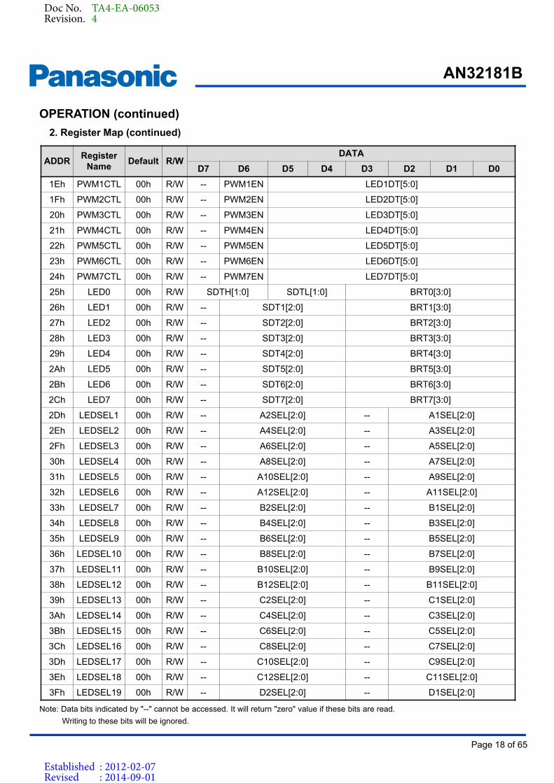
OPERATION (continued)
Doc No. TA4-EA-06053Revision. 4
Established : 2012-02-07Revised : 2014-09-01
AN32181B
Page 18 of 65
Product Standards
ADDRRegister
NameDefault R/W
DATA
D7 D6 D5 D4 D3 D2 D1 D0
1Eh PWM1CTL 00h R/W -- PWM1EN LED1DT[5:0]
1Fh PWM2CTL 00h R/W -- PWM2EN LED2DT[5:0]
20h PWM3CTL 00h R/W -- PWM3EN LED3DT[5:0]
21h PWM4CTL 00h R/W -- PWM4EN LED4DT[5:0]
22h PWM5CTL 00h R/W -- PWM5EN LED5DT[5:0]
23h PWM6CTL 00h R/W -- PWM6EN LED6DT[5:0]
24h PWM7CTL 00h R/W -- PWM7EN LED7DT[5:0]
25h LED0 00h R/W SDTH[1:0] SDTL[1:0] BRT0[3:0]
26h LED1 00h R/W -- SDT1[2:0] BRT1[3:0]
27h LED2 00h R/W -- SDT2[2:0] BRT2[3:0]
28h LED3 00h R/W -- SDT3[2:0] BRT3[3:0]
29h LED4 00h R/W -- SDT4[2:0] BRT4[3:0]
2Ah LED5 00h R/W -- SDT5[2:0] BRT5[3:0]
2Bh LED6 00h R/W -- SDT6[2:0] BRT6[3:0]
2Ch LED7 00h R/W -- SDT7[2:0] BRT7[3:0]
2Dh LEDSEL1 00h R/W -- A2SEL[2:0] -- A1SEL[2:0]
2Eh LEDSEL2 00h R/W -- A4SEL[2:0] -- A3SEL[2:0]
2Fh LEDSEL3 00h R/W -- A6SEL[2:0] -- A5SEL[2:0]
30h LEDSEL4 00h R/W -- A8SEL[2:0] -- A7SEL[2:0]
31h LEDSEL5 00h R/W -- A10SEL[2:0] -- A9SEL[2:0]
32h LEDSEL6 00h R/W -- A12SEL[2:0] -- A11SEL[2:0]
33h LEDSEL7 00h R/W -- B2SEL[2:0] -- B1SEL[2:0]
34h LEDSEL8 00h R/W -- B4SEL[2:0] -- B3SEL[2:0]
35h LEDSEL9 00h R/W -- B6SEL[2:0] -- B5SEL[2:0]
36h LEDSEL10 00h R/W -- B8SEL[2:0] -- B7SEL[2:0]
37h LEDSEL11 00h R/W -- B10SEL[2:0] -- B9SEL[2:0]
38h LEDSEL12 00h R/W -- B12SEL[2:0] -- B11SEL[2:0]
39h LEDSEL13 00h R/W -- C2SEL[2:0] -- C1SEL[2:0]
3Ah LEDSEL14 00h R/W -- C4SEL[2:0] -- C3SEL[2:0]
3Bh LEDSEL15 00h R/W -- C6SEL[2:0] -- C5SEL[2:0]
3Ch LEDSEL16 00h R/W -- C8SEL[2:0] -- C7SEL[2:0]
3Dh LEDSEL17 00h R/W -- C10SEL[2:0] -- C9SEL[2:0]
3Eh LEDSEL18 00h R/W -- C12SEL[2:0] -- C11SEL[2:0]
3Fh LEDSEL19 00h R/W -- D2SEL[2:0] -- D1SEL[2:0]
Note: Data bits indicated by "--" cannot be accessed. It will return "zero" value if these bits are read.
Writing to these bits will be ignored.
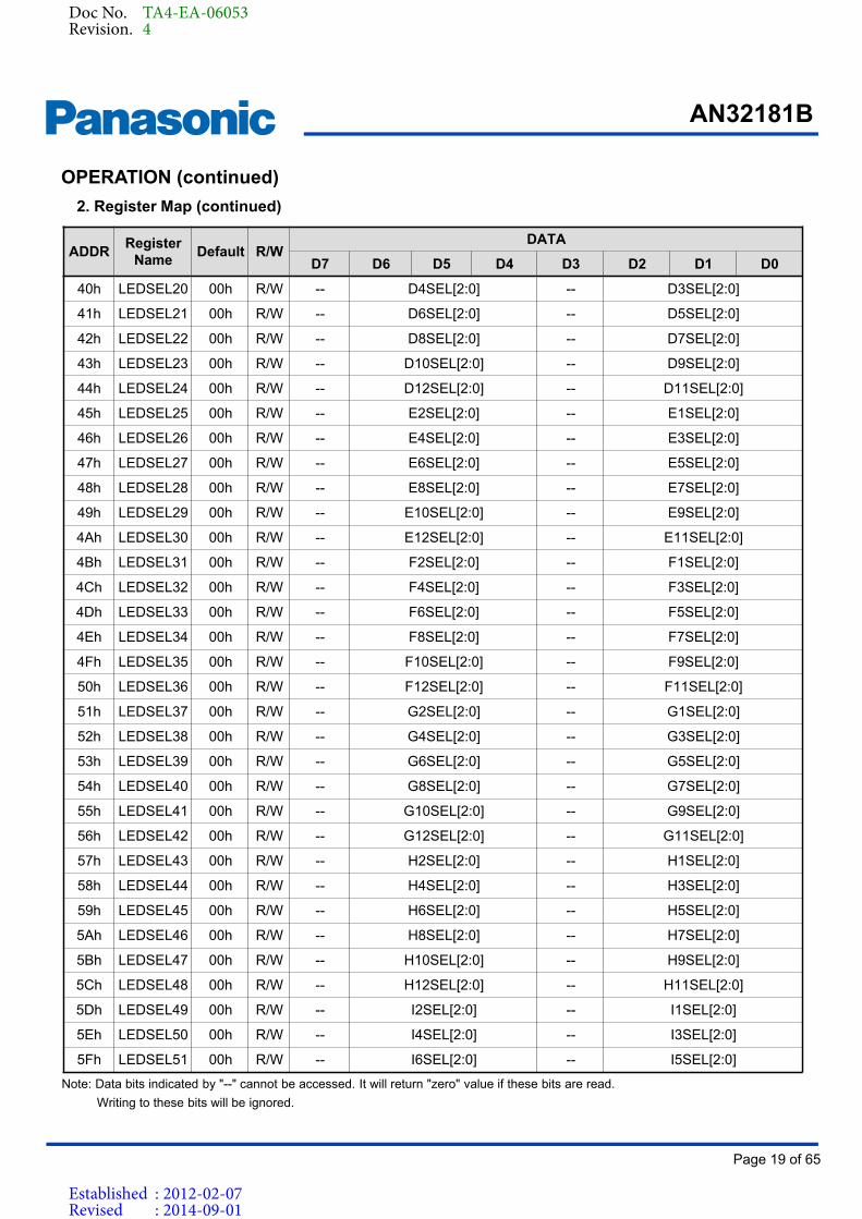
2. Register Map (continued)
OPERATION (continued)
Doc No. TA4-EA-06053Revision. 4
Established : 2012-02-07Revised : 2014-09-01
AN32181B
Page 19 of 65
Product Standards
ADDRRegister
NameDefault R/W
DATA
D7 D6 D5 D4 D3 D2 D1 D0
40h LEDSEL20 00h R/W -- D4SEL[2:0] -- D3SEL[2:0]
41h LEDSEL21 00h R/W -- D6SEL[2:0] -- D5SEL[2:0]
42h LEDSEL22 00h R/W -- D8SEL[2:0] -- D7SEL[2:0]
43h LEDSEL23 00h R/W -- D10SEL[2:0] -- D9SEL[2:0]
44h LEDSEL24 00h R/W -- D12SEL[2:0] -- D11SEL[2:0]
45h LEDSEL25 00h R/W -- E2SEL[2:0] -- E1SEL[2:0]
46h LEDSEL26 00h R/W -- E4SEL[2:0] -- E3SEL[2:0]
47h LEDSEL27 00h R/W -- E6SEL[2:0] -- E5SEL[2:0]
48h LEDSEL28 00h R/W -- E8SEL[2:0] -- E7SEL[2:0]
49h LEDSEL29 00h R/W -- E10SEL[2:0] -- E9SEL[2:0]
4Ah LEDSEL30 00h R/W -- E12SEL[2:0] -- E11SEL[2:0]
4Bh LEDSEL31 00h R/W -- F2SEL[2:0] -- F1SEL[2:0]
4Ch LEDSEL32 00h R/W -- F4SEL[2:0] -- F3SEL[2:0]
4Dh LEDSEL33 00h R/W -- F6SEL[2:0] -- F5SEL[2:0]
4Eh LEDSEL34 00h R/W -- F8SEL[2:0] -- F7SEL[2:0]
4Fh LEDSEL35 00h R/W -- F10SEL[2:0] -- F9SEL[2:0]
50h LEDSEL36 00h R/W -- F12SEL[2:0] -- F11SEL[2:0]
51h LEDSEL37 00h R/W -- G2SEL[2:0] -- G1SEL[2:0]
52h LEDSEL38 00h R/W -- G4SEL[2:0] -- G3SEL[2:0]
53h LEDSEL39 00h R/W -- G6SEL[2:0] -- G5SEL[2:0]
54h LEDSEL40 00h R/W -- G8SEL[2:0] -- G7SEL[2:0]
55h LEDSEL41 00h R/W -- G10SEL[2:0] -- G9SEL[2:0]
56h LEDSEL42 00h R/W -- G12SEL[2:0] -- G11SEL[2:0]
57h LEDSEL43 00h R/W -- H2SEL[2:0] -- H1SEL[2:0]
58h LEDSEL44 00h R/W -- H4SEL[2:0] -- H3SEL[2:0]
59h LEDSEL45 00h R/W -- H6SEL[2:0] -- H5SEL[2:0]
5Ah LEDSEL46 00h R/W -- H8SEL[2:0] -- H7SEL[2:0]
5Bh LEDSEL47 00h R/W -- H10SEL[2:0] -- H9SEL[2:0]
5Ch LEDSEL48 00h R/W -- H12SEL[2:0] -- H11SEL[2:0]
5Dh LEDSEL49 00h R/W -- I2SEL[2:0] -- I1SEL[2:0]
5Eh LEDSEL50 00h R/W -- I4SEL[2:0] -- I3SEL[2:0]
5Fh LEDSEL51 00h R/W -- I6SEL[2:0] -- I5SEL[2:0]
Note: Data bits indicated by "--" cannot be accessed. It will return "zero" value if these bits are read.
Writing to these bits will be ignored.
2. Register Map (continued)
OPERATION (continued)
Doc No. TA4-EA-06053Revision. 4
Established : 2012-02-07Revised : 2014-09-01
AN32181B
Page 20 of 65
Product Standards
ADDRRegister
NameDefault R/W
DATA
D7 D6 D5 D4 D3 D2 D1 D0
60h LEDSEL52 00h R/W -- I8SEL[2:0] -- I7SEL[2:0]
61h LEDSEL53 00h R/W -- I10SEL[2:0] -- I9SEL[2:0]
62h LEDSEL54 00h R/W -- I12SEL[2:0] -- I11SEL[2:0]
63h LEDSEL55 00h R/W -- J2SEL[2:0] -- J1SEL[2:0]
64h LEDSEL56 00h R/W -- J4SEL[2:0] -- J3SEL[2:0]
65h LEDSEL57 00h R/W -- J6SEL[2:0] -- J5SEL[2:0]
66h LEDSEL58 00h R/W -- J8SEL[2:0] -- J7SEL[2:0]
67h LEDSEL59 00h R/W -- J10SEL[2:0] -- J9SEL[2:0]
68h LEDSEL60 00h R/W -- J12SEL[2:0] -- J11SEL[2:0]
69h LEDSEL61 00h R/W -- K2SEL[2:0] -- K1SEL[2:0]
6Ah LEDSEL62 00h R/W -- K4SEL[2:0] -- K3SEL[2:0]
6Bh LEDSEL63 00h R/W -- K6SEL[2:0] -- K5SEL[2:0]
6Ch LEDSEL64 00h R/W -- K8SEL[2:0] -- K7SEL[2:0]
6Dh LEDSEL65 00h R/W -- K10SEL[2:0] -- K9SEL[2:0]
6Eh LEDSEL66 00h R/W -- K12SEL[2:0] -- K11SEL[2:0]
6Fh LEDSEL67 00h R/W -- L2SEL[2:0] -- L1SEL[2:0]
70h LEDSEL68 00h R/W -- L4SEL[2:0] -- L3SEL[2:0]
71h LEDSEL69 00h R/W -- L6SEL[2:0] -- L5SEL[2:0]
72h LEDSEL70 00h R/W -- L8SEL[2:0] -- L7SEL[2:0]
73h LEDSEL71 00h R/W -- L10SEL[2:0] -- L9SEL[2:0]
74h LEDSEL72 00h R/W -- L12SEL[2:0] -- L11SEL[2:0]
75h SCROLL1 00h R/W -- E_STOP D_STOP C_STOP B_STOP A_STOP UP LEFT
76h SCROLL2 00h R/W -- -- -- -- -- SCLTIME[2:0]
77h XCONST1 00h R/W X8CONST X7CONST X6CONST X5CONST X4CONST X3CONST X2CONST X1CONST
78h XCONST2 00h R/W -- -- --X13
CONST
X12
CONST
X11
CONST
X10
CONST
X9
CONST
79h YMSK1 00h R/W Y8MSK Y7MSK Y6MSK Y5MSK Y4MSK Y3MSK Y2MSK Y1MSK
7Ah YMSK2 00h R/W -- -- -- YMSKVAL Y12MSK Y11MSK Y10MSK Y9MSK
7Bh reserved -- -- -- -- -- -- -- -- -- --
7Ch reserved -- -- -- -- -- -- -- -- -- --
7Dh reserved -- -- -- -- -- -- -- -- -- --
7Eh SCANSET 0Bh R/W -- -- -- -- SCANSET[3:0]
7Fh reserved -- -- -- -- -- -- -- -- -- --
Note) "Reserved" registers and data bits indicated by "--" cannot be accessed. "Reserved" registers are not used.
For data bits indicated by "--" in other registers except from "reversed" registers, will return "zero" value if these bits are read.
Writing to these bits will be ignored.
2. Register Map (continued)
OPERATION (continued)
Doc No. TA4-EA-06053Revision. 4
Established : 2012-02-07Revised : 2014-09-01
AN32181B
Page 21 of 65
Product Standards
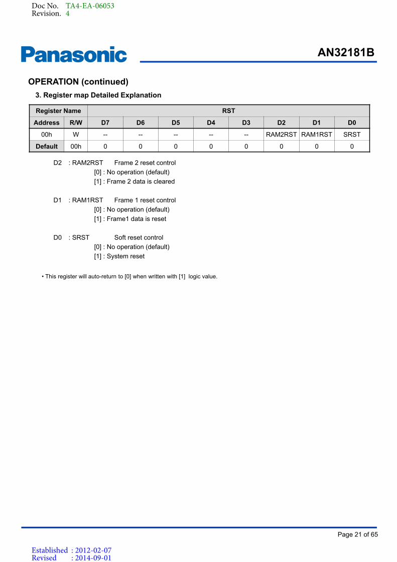
Register Name RST
Address R/W D7 D6 D5 D4 D3 D2 D1 D0
00h W -- -- -- -- -- RAM2RST RAM1RST SRST
Default 00h 0 0 0 0 0 0 0 0
D2 : RAM2RST Frame 2 reset control
[0] : No operation (default)
[1] : Frame 2 data is cleared
D1 : RAM1RST Frame 1 reset control
[0] : No operation (default)
[1] : Frame1 data is reset
D0 : SRST Soft reset control
[0] : No operation (default)
[1] : System reset
• This register will auto-return to [0] when written with [1] logic value.
3. Register map Detailed Explanation
OPERATION (continued)
Doc No. TA4-EA-06053Revision. 4
Established : 2012-02-07Revised : 2014-09-01
AN32181B
Page 22 of 65
Product Standards
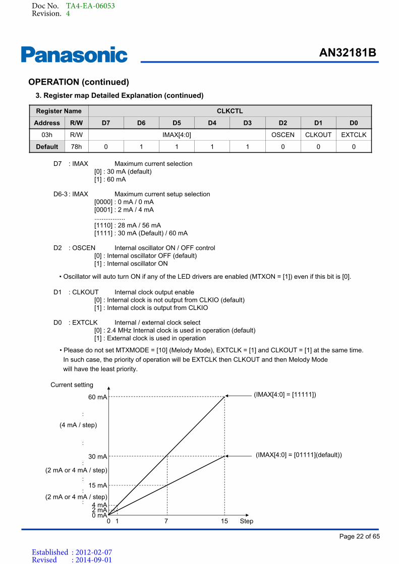
Register Name CLKCTL
Address R/W D7 D6 D5 D4 D3 D2 D1 D0
03h R/W IMAX[4:0] OSCEN CLKOUT EXTCLK
Default 78h 0 1 1 1 1 0 0 0
D7 : IMAX Maximum current selection[0] : 30 mA (default)[1] : 60 mA
D6-3 : IMAX Maximum current setup selection[0000] : 0 mA / 0 mA[0001] : 2 mA / 4 mA.................[1110] : 28 mA / 56 mA[1111] : 30 mA (Default) / 60 mA
D2 : OSCEN Internal oscillator ON / OFF control[0] : Internal oscillator OFF (default)[1] : Internal oscillator ON
D1 : CLKOUT Internal clock output enable[0] : Internal clock is not output from CLKIO (default)[1] : Internal clock is output from CLKIO
D0 : EXTCLK Internal / external clock select[0] : 2.4 MHz Internal clock is used in operation (default)[1] : External clock is used in operation
Current setting
1 7
30 mA
Step
15 mA
2 mA
15
(2 mA or 4 mA / step):
:
(2 mA or 4 mA / step):
:
00 mA
60 mA
4 mA
(4 mA / step)
:
:
(IMAX[4:0] = [01111](default))
(IMAX[4:0] = [11111])
• Oscillator will auto turn ON if any of the LED drivers are enabled (MTXON = [1]) even if this bit is [0].
• Please do not set MTXMODE = [10] (Melody Mode), EXTCLK = [1] and CLKOUT = [1] at the same time.
In such case, the priority of operation will be EXTCLK then CLKOUT and then Melody Mode
will have the least priority.
3. Register map Detailed Explanation (continued)
OPERATION (continued)
Doc No. TA4-EA-06053Revision. 4
Established : 2012-02-07Revised : 2014-09-01
AN32181B
Page 23 of 65
Product Standards
Register Name MTXON
Address R/W D7 D6 D5 D4 D3 D2 D1 D0
04h R/W -- -- -- -- ZPDEN MTXMODE[1:0] MTXON
Default 00h 0 0 0 0 0 0 0 0
D3 : ZPDEN Ghost image prevention function enable[0] : Turn off ghost image prevention (default)[1] : Turn on ghost image prevention
D2-1 : MTXMODE Matrix mode of operation select
[00] : Display Matrix frame 1 character (default)
[01] : Display Matrix frame 2 character
[10] : Melody Mode
[11] : Scroll Mode
D0 : MTXON Matrix ON / OFF setting
[0] : OFF (default)
[1] : ON
Register Name FRMSEL
Address R/W D7 D6 D5 D4 D3 D2 D1 D0
05h R/W -- -- -- -- -- -- -- FRMSEL
Default 00h 0 0 0 0 0 0 0 0
D0 : FRMSEL
(1) Normal Modes :
[0] : Matrix Frame 1 is selected for character write (default).
[1] : Matrix Frame 2 is selected for character write.
(2) Melody Mode :
[0] : Matrix Frame 1 is selected for character write (default).
[1] : Matrix Frame 2 is selected for melody enable for each LED.
• During scroll mode, FRMSEL need not be set. Frame to be written is automatically selected whichever
is free.
3. Register map Detailed Explanation (continued)
OPERATION (continued)
• Ghost Image Prevention may not remove the ghost image perfectly. It depends on
the LED color combination and LED connection method. Please refer to Page.59 for details.
• Please refer to Page.60 for details especially when this IC is used for RGB driver.
Doc No. TA4-EA-06053Revision. 4
Established : 2012-02-07Revised : 2014-09-01
AN32181B
Page 24 of 65
Product Standards
Register Name MTXON1
Address R/W D7 D6 D5 D4 D3 D2 D1 D0
06h W A8ON A7ON A6ON A5ON A4ON A3ON A2ON A1ON
Default 00h 0 0 0 0 0 0 0 0
D7 : A8ON
(1) Normal Mode : LED A8 of Matrix ON / OFF control
[0] : OFF (default)
[1] : ON
(2) Melody Mode & FRMSEL = [1] : LED A8 of Matrix Melody Mode ON / OFF control
[0] : LED A8 Melody Mode OFF (default)
[1] : LED A8 Melody Mode ON
...
D0 : A1ON
(1) Normal Mode : LED A1 of Matrix ON / OFF control
[0] : OFF (default)
[1] : ON
(2) Melody Mode & FRMSEL = [1] : LED A1 of Matrix Melody Mode ON / OFF control
[0] : LED A1 Melody Mode OFF (default)
[1] : LED A1 Melody Mode ON
OFF
ON
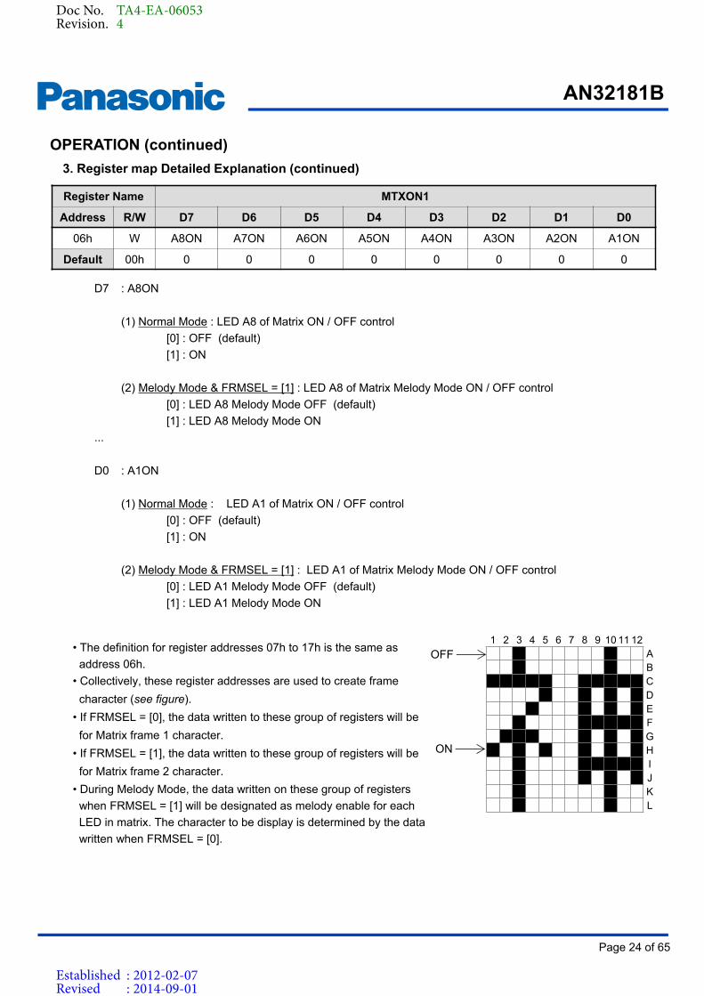
1 2 3 4 5 6 7 8 9 10 11 12ABCDEFGHIJKL
• The definition for register addresses 07h to 17h is the same as
address 06h.
• Collectively, these register addresses are used to create frame
character (see figure).
• If FRMSEL = [0], the data written to these group of registers will be
for Matrix frame 1 character.
• If FRMSEL = [1], the data written to these group of registers will be
for Matrix frame 2 character.
• During Melody Mode, the data written on these group of registers
when FRMSEL = [1] will be designated as melody enable for each
LED in matrix. The character to be display is determined by the data
written when FRMSEL = [0].
3. Register map Detailed Explanation (continued)
OPERATION (continued)
Doc No. TA4-EA-06053Revision. 4
Established : 2012-02-07Revised : 2014-09-01
AN32181B
Page 25 of 65
Product Standards
Register Name THOLD
Address R/W D7 D6 D5 D4 D3 D2 D1 D0
18h R/W THOLD[7:0]
Default 00h 0 0 0 0 0 0 0 0
D7 : THOLD[7] Threshold 8 is used as voltage detection.
[0] : Others (default)
[1] : Threshold 8 is used. (Threshold 8 is about 1.93 V)
D6 : THOLD[6] Threshold 7 is used as voltage detection.
[0] : Others (default)
[1] : Threshold 7 is used. (Threshold 7 is about 1.80 V)
D5 : THOLD[5] Threshold 6 is used as voltage detection.
[0] : Others (default)
[1] : Threshold 6 is used. (Threshold 6 is about 1.67 V)
D4 : THOLD[4] Threshold 5 is used as voltage detection.
[0] : Others (default)
[1] : Threshold 5 is used. (Threshold 5 is about 1.55 V)
D3 : THOLD[3] Threshold 4 is used as voltage detection.
[0] : Others (default)
[1] : Threshold 4 is used. (Threshold 4 is about 1.42 V)
D2 : THOLD[2] Threshold 3 is used as voltage detection.
[0] : Others (default)
[1] : Threshold 3 is used. (Threshold 3 is about 1.30 V)
D1 : THOLD[1] Threshold 2 is used as voltage detection.
[0] : Others (default)
[1] : Threshold 2 is used. (Threshold 2 is about 1.17 V)
D0 : THOLD[0] Threshold 1 is used as voltage detection.
[0] : Others (default)
[1] : Threshold 1 is used. (Threshold 1 is about 1.04 V)
• When all bits are set [0], threshold is in auto-detection mode (default)
• Do not set more than 1 register bit to logic [1] value at the same time.
• If 2 bits are set to [1] at the same time, system will only recognize the first [1] bit threshold that
is set.
3. Register map Detailed Explanation (continued)
OPERATION (continued)
Doc No. TA4-EA-06053Revision. 4
Established : 2012-02-07Revised : 2014-09-01
AN32181B
Page 26 of 65
Product Standards
Register Name MELODY
Address R/W D7 D6 D5 D4 D3 D2 D1 D0
19h R/W -- MLDCOM[2:0] GRP4 GRP3 GRP2 GRP1
Default 00h 0 0 0 0 0 0 0 0
D6-4 : MLDCOM Brightness compensation in melody mode[000] : No Compensation (default)[001] : PWM duty + 12.5 %[010] : PWM duty + 25.0 %[011] : PWM duty + 37.5 %[100] : PWM duty + 50.0 %[101] : PWM duty + 62.5 %[110] : PWM duty + 75.0 %[111] : PWM duty + 87.5 %
D3 : GRP4 Group 4 LED melody control[0] : Normal operation (default)[1] : During melody mode, Group 4 LEDs are synchronized to external source as bar meter.
D2 : GRP3 Group 3 LED melody control[0] : Normal operation (default)[1] : During melody mode, Group 3 LEDs are synchronized to external source as bar meter.
D1 : GRP2 Group 2 LED melody control[0] : Normal operation (default)[1] : During melody mode, Group 2 LEDs are synchronized to external source as bar meter.
D0 : GRP1 Group 1 LED melody control[0] : Normal operation (default)[1] : During melody mode, Group 1 LEDs are synchronized to external source as bar meter.
¯1 2 3 4 5 6 7 8 9 10 11 12
ABCDEFG
H
IJKL
• During Bar Meter Mode, auto threshold detection should be used.
This IC does not support Bar Meter Mode with fixed threshold setting.
Grp1
Grp2
Grp3
Grp4
Threshold 1
…
Threshold 2
Threshold 3
Threshold 8
3. Register map Detailed Explanation (continued)
OPERATION (continued)
Doc No. TA4-EA-06053Revision. 4
Established : 2012-02-07Revised : 2014-09-01

AN32181B
Page 27 of 65
Product Standards
Register Name INTREG
Address R/W D7 D6 D5 D4 D3 D2 D1 D0
1Ah R/W -- -- -- -- TSTEND OPEN SHORT FRMINT
Default 00h 0 0 0 0 0 0 0 0
D3 : TSTEND Indicates the LED test finish
[0] : Normal operation (default)
[1] : LED detection finished
D2 : OPEN Indicates open circuit is detected
[0] : Normal operation (default)
[1] : Open circuit detected
D1 : SHORT Indicates short circuit is detected
[0] : Normal operation (default)
[1] : Short circuit detected
D0 : FRMINT Indicate end of scroll of one frame
[0] : Normal operation (default)
[1] : End of frame.
• Any bit in this register will cause INT pin to go "Low".
• To clear interrupt, write [0] to corresponding bit.
• Writing [1] to these bits will be ignored.
3. Register map Detailed Explanation (continued)
OPERATION (continued)
Doc No. TA4-EA-06053Revision. 4
Established : 2012-02-07Revised : 2014-09-01
AN32181B
Page 28 of 65
Product Standards
Register Name INTMSK
Address R/W D7 D6 D5 D4 D3 D2 D1 D0
1Bh R/W -- -- -- -- TSTMSK OPMSK SHMSK FRMMSK
Default 0Fh 0 0 0 0 1 1 1 1
Register Name DETECT
Address R/W D7 D6 D5 D4 D3 D2 D1 D0
1Ch W -- -- -- -- -- -- -- DETECT
Default 00h 0 0 0 0 0 0 0 0
D3 : TSTMSK TSTEND interrupt mask register
[0] : Interrupt is not masked.
[1] : Interrupt is masked. (default).
D2 : OPMSK Open error interrupt mask register
[0] : Interrupt is not masked.
[1] : Interrupt is masked. (default).
D1 : SHMSK Shorted error interrupt mask register
[0] : Interrupt is not masked.
[1] : Interrupt is masked. (default).
D0 : FRMMSK Frame interrupt mask register
[0] : Interrupt is not masked.
[1] : Interrupt is masked. (default).
D0 : DETECT Open/short detection enable
[0] : detection is OFF (default)
[1] : detection is ON
• Enabling this register will also enable the matrix operation. Don't set MTXON and DETECT both to
[1] at same time.
3. Register map Detailed Explanation (continued)
OPERATION (continued)
Doc No. TA4-EA-06053Revision. 4
Established : 2012-02-07Revised : 2014-09-01
AN32181B
Page 29 of 65
Product Standards
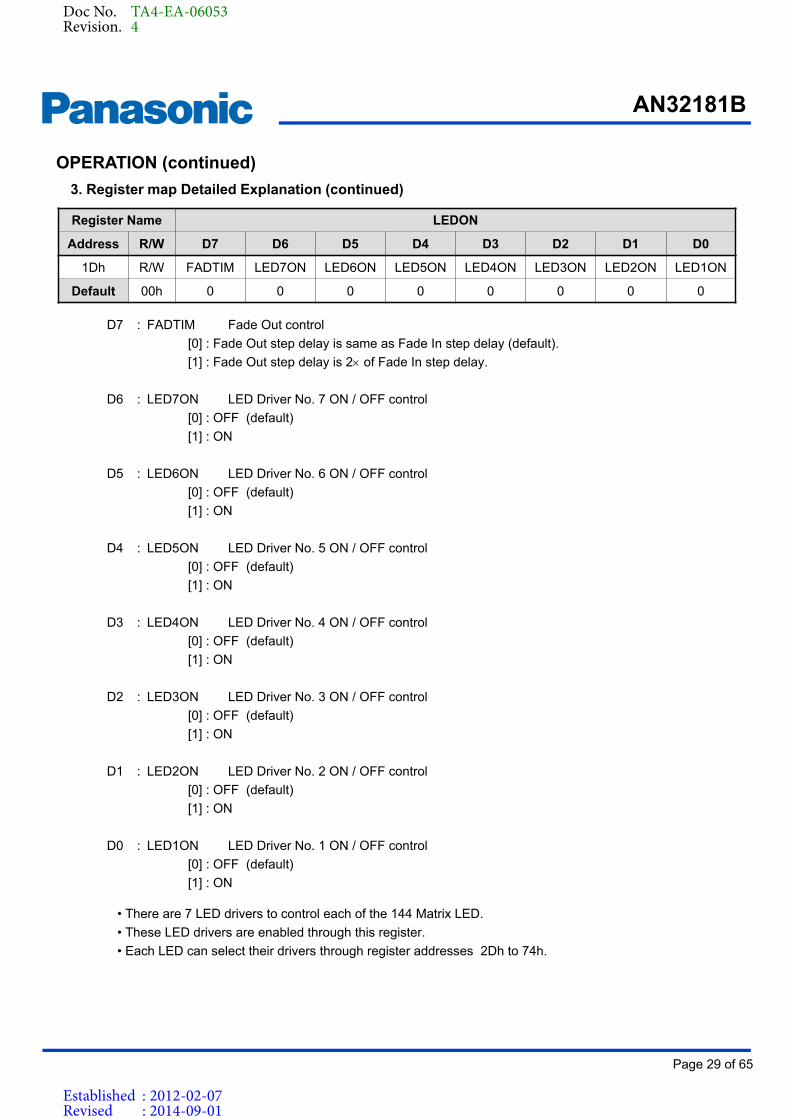
Register Name LEDON
Address R/W D7 D6 D5 D4 D3 D2 D1 D0
1Dh R/W FADTIM LED7ON LED6ON LED5ON LED4ON LED3ON LED2ON LED1ON
Default 00h 0 0 0 0 0 0 0 0
D7 : FADTIM Fade Out control
[0] : Fade Out step delay is same as Fade In step delay (default).
[1] : Fade Out step delay is 2 of Fade In step delay.
D6 : LED7ON LED Driver No. 7 ON / OFF control
[0] : OFF (default)
[1] : ON
D5 : LED6ON LED Driver No. 6 ON / OFF control
[0] : OFF (default)
[1] : ON
D4 : LED5ON LED Driver No. 5 ON / OFF control
[0] : OFF (default)
[1] : ON
D3 : LED4ON LED Driver No. 4 ON / OFF control
[0] : OFF (default)
[1] : ON
D2 : LED3ON LED Driver No. 3 ON / OFF control
[0] : OFF (default)
[1] : ON
D1 : LED2ON LED Driver No. 2 ON / OFF control
[0] : OFF (default)
[1] : ON
D0 : LED1ON LED Driver No. 1 ON / OFF control
[0] : OFF (default)
[1] : ON
• There are 7 LED drivers to control each of the 144 Matrix LED.
• These LED drivers are enabled through this register.
• Each LED can select their drivers through register addresses 2Dh to 74h.
3. Register map Detailed Explanation (continued)
OPERATION (continued)
Doc No. TA4-EA-06053Revision. 4
Established : 2012-02-07Revised : 2014-09-01
AN32181B
Page 30 of 65
Product Standards
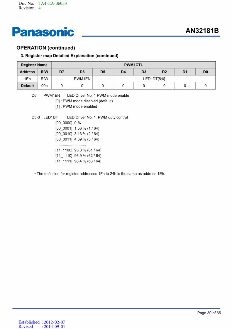
Register Name PWM1CTL
Address R/W D7 D6 D5 D4 D3 D2 D1 D0
1Eh R/W -- PWM1EN LED1DT[5:0]
Default 00h 0 0 0 0 0 0 0 0
D6 : PWM1EN LED Driver No. 1 PWM mode enable
[0] : PWM mode disabled (default)
[1] : PWM mode enabled
D5-0 : LED1DT LED Driver No. 1 PWM duty control
[00_0000] 0 %
[00_0001] 1.56 % (1 / 64)
[00_0010] 3.13 % (2 / 64)
[00_0011] 4.69 % (3 / 64)
............................
[11_1100] 95.3 % (61 / 64)
[11_1110] 96.9 % (62 / 64)
[11_1111] 98.4 % (63 / 64)
• The definition for register addresses 1Fh to 24h is the same as address 1Eh.
3. Register map Detailed Explanation (continued)
OPERATION (continued)
Doc No. TA4-EA-06053Revision. 4
Established : 2012-02-07Revised : 2014-09-01
AN32181B
Page 31 of 65
Product Standards
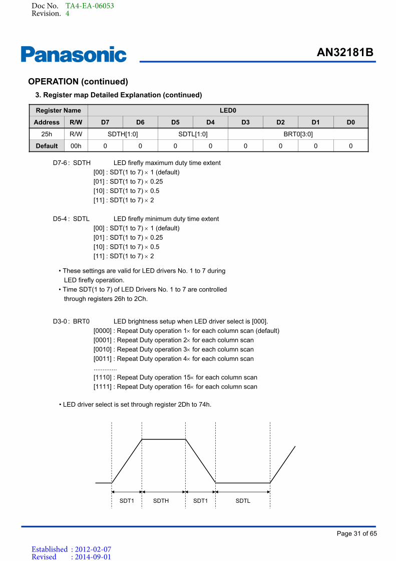
Register Name LED0
Address R/W D7 D6 D5 D4 D3 D2 D1 D0
25h R/W SDTH[1:0] SDTL[1:0] BRT0[3:0]
Default 00h 0 0 0 0 0 0 0 0
D7-6 : SDTH LED firefly maximum duty time extent
[00] : SDT(1 to 7) 1 (default)
[01] : SDT(1 to 7) 0.25
[10] : SDT(1 to 7) 0.5
[11] : SDT(1 to 7) 2
D5-4 : SDTL LED firefly minimum duty time extent
[00] : SDT(1 to 7) 1 (default)
[01] : SDT(1 to 7) 0.25
[10] : SDT(1 to 7) 0.5
[11] : SDT(1 to 7) 2
D3-0 : BRT0 LED brightness setup when LED driver select is [000].
[0000] : Repeat Duty operation 1 for each column scan (default)
[0001] : Repeat Duty operation 2 for each column scan
[0010] : Repeat Duty operation 3 for each column scan
[0011] : Repeat Duty operation 4 for each column scan
.............
[1110] : Repeat Duty operation 15 for each column scan
[1111] : Repeat Duty operation 16 for each column scan
SDT1 SDTH SDT1 SDTL
• These settings are valid for LED drivers No. 1 to 7 during
LED firefly operation.
• Time SDT(1 to 7) of LED Drivers No. 1 to 7 are controlled
through registers 26h to 2Ch.
• LED driver select is set through register 2Dh to 74h.
3. Register map Detailed Explanation (continued)
OPERATION (continued)
Doc No. TA4-EA-06053Revision. 4
Established : 2012-02-07Revised : 2014-09-01
AN32181B
Page 32 of 65
Product Standards
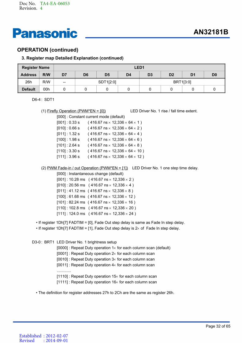
Register Name LED1
Address R/W D7 D6 D5 D4 D3 D2 D1 D0
26h R/W -- SDT1[2:0] BRT1[3:0]
Default 00h 0 0 0 0 0 0 0 0
D6-4 : SDT1
(1) Firefly Operation (PWM*EN = [0]) LED Driver No. 1 rise / fall time extent.
[000] : Constant current mode (default)
[001] : 0.33 s ( 416.67 ns 12,336 64 1 )
[010] : 0.66 s ( 416.67 ns 12,336 64 2 )
[011] : 1.32 s ( 416.67 ns 12,336 64 4 )
[100] : 1.98 s ( 416.67 ns 12,336 64 6 )
[101] : 2.64 s ( 416.67 ns 12,336 64 8 )
[110] : 3.30 s ( 416.67 ns 12,336 64 10 )
[111] : 3.96 s ( 416.67 ns 12,336 64 12 )
(2) PWM Fade-in / out Operation (PWM*EN = [1]) LED Driver No. 1 one step time delay.
[000] : Instantaneous change (default)
[001] : 10.28 ms ( 416.67 ns 12,336 2 )
[010] : 20.56 ms ( 416.67 ns 12,336 4 )
[011] : 41.12 ms ( 416.67 ns 12,336 8 )
[100] : 61.68 ms ( 416.67 ns 12,336 12 )
[101] : 82.24 ms ( 416.67 ns 12,336 16 )
[110] : 102.8 ms ( 416.67 ns 12,336 20 )
[111] : 124.0 ms ( 416.67 ns 12,336 24 )
D3-0 : BRT1 LED Driver No. 1 brightness setup
[0000] : Repeat Duty operation 1 for each column scan (default)
[0001] : Repeat Duty operation 2 for each column scan
[0010] : Repeat Duty operation 3 for each column scan
[0011] : Repeat Duty operation 4 for each column scan
.............
[1110] : Repeat Duty operation 15 for each column scan
[1111] : Repeat Duty operation 16 for each column scan
• If register 1Dh[7] FADTIM = [0], Fade Out step delay is same as Fade In step delay.
• If register 1Dh[7] FADTIM = [1], Fade Out step delay is 2 of Fade In step delay.
• The definition for register addresses 27h to 2Ch are the same as register 26h.
3. Register map Detailed Explanation (continued)
OPERATION (continued)
Doc No. TA4-EA-06053Revision. 4
Established : 2012-02-07Revised : 2014-09-01
AN32181B
Page 33 of 65
Product Standards
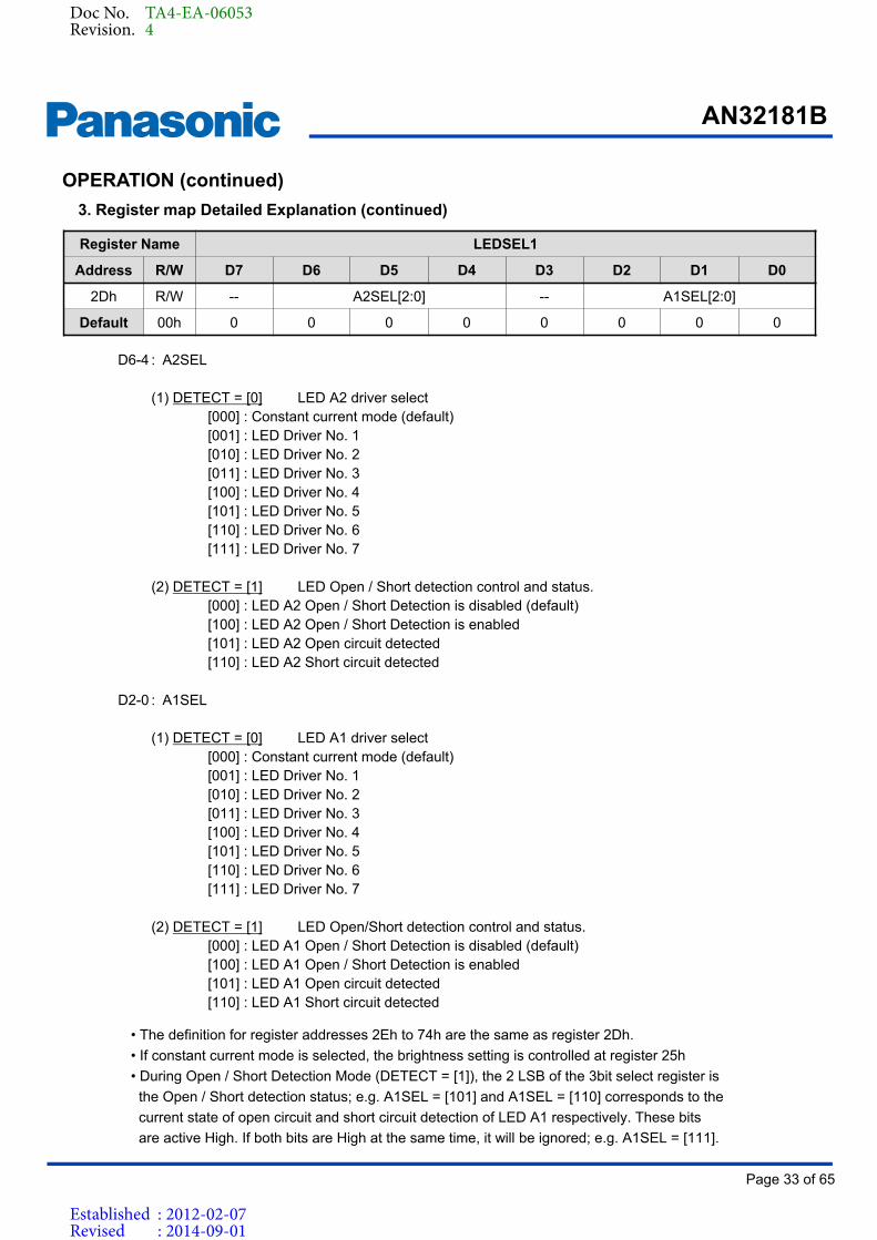
Register Name LEDSEL1
Address R/W D7 D6 D5 D4 D3 D2 D1 D0
2Dh R/W -- A2SEL[2:0] -- A1SEL[2:0]
Default 00h 0 0 0 0 0 0 0 0
D6-4 : A2SEL
(1) DETECT = [0] LED A2 driver select[000] : Constant current mode (default)[001] : LED Driver No. 1[010] : LED Driver No. 2[011] : LED Driver No. 3[100] : LED Driver No. 4[101] : LED Driver No. 5[110] : LED Driver No. 6[111] : LED Driver No. 7
(2) DETECT = [1] LED Open / Short detection control and status.[000] : LED A2 Open / Short Detection is disabled (default)[100] : LED A2 Open / Short Detection is enabled[101] : LED A2 Open circuit detected[110] : LED A2 Short circuit detected
D2-0 : A1SEL
(1) DETECT = [0] LED A1 driver select[000] : Constant current mode (default)[001] : LED Driver No. 1[010] : LED Driver No. 2[011] : LED Driver No. 3[100] : LED Driver No. 4[101] : LED Driver No. 5[110] : LED Driver No. 6[111] : LED Driver No. 7
(2) DETECT = [1] LED Open/Short detection control and status.[000] : LED A1 Open / Short Detection is disabled (default)[100] : LED A1 Open / Short Detection is enabled[101] : LED A1 Open circuit detected[110] : LED A1 Short circuit detected
• The definition for register addresses 2Eh to 74h are the same as register 2Dh.
• If constant current mode is selected, the brightness setting is controlled at register 25h
• During Open / Short Detection Mode (DETECT = [1]), the 2 LSB of the 3bit select register is
the Open / Short detection status; e.g. A1SEL = [101] and A1SEL = [110] corresponds to the
current state of open circuit and short circuit detection of LED A1 respectively. These bits
are active High. If both bits are High at the same time, it will be ignored; e.g. A1SEL = [111].
3. Register map Detailed Explanation (continued)
OPERATION (continued)
Doc No. TA4-EA-06053Revision. 4
Established : 2012-02-07Revised : 2014-09-01
AN32181B
Page 34 of 65
Product Standards
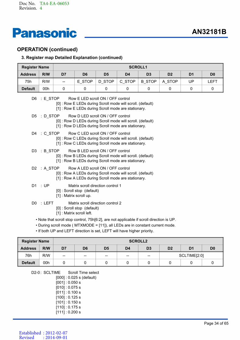
Register Name SCROLL1
Address R/W D7 D6 D5 D4 D3 D2 D1 D0
75h R/W -- E_STOP D_STOP C_STOP B_STOP A_STOP UP LEFT
Default 00h 0 0 0 0 0 0 0 0
Register Name SCROLL2
Address R/W D7 D6 D5 D4 D3 D2 D1 D0
76h R/W -- -- -- -- -- SCLTIME[2:0]
Default 00h 0 0 0 0 0 0 0 0
D6 : E_STOP Row E LED scroll ON / OFF control[0] : Row E LEDs during Scroll mode will scroll. (default)[1] : Row E LEDs during Scroll mode are stationary.
D5 : D_STOP Row D LED scroll ON / OFF control[0] : Row D LEDs during Scroll mode will scroll. (default)[1] : Row D LEDs during Scroll mode are stationary.
D4 : C_STOP Row C LED scroll ON / OFF control[0] : Row C LEDs during Scroll mode will scroll. (default)[1] : Row C LEDs during Scroll mode are stationary.
D3 : B_STOP Row B LED scroll ON / OFF control[0] : Row B LEDs during Scroll mode will scroll. (default)[1] : Row B LEDs during Scroll mode are stationary.
D2 : A_STOP Row A LED scroll ON / OFF control[0] : Row A LEDs during Scroll mode will scroll. (default)[1] : Row A LEDs during Scroll mode are stationary.
D1 : UP Matrix scroll direction control 1[0] : Scroll stop (default)[1] : Matrix scroll up.
D0 : LEFT Matrix scroll direction control 2[0] : Scroll stop (default)[1] : Matrix scroll left.
D2-0 : SCLTIME Scroll Time select[000] : 0.025 s (default)[001] : 0.050 s[010] : 0.075 s[011] : 0.100 s[100] : 0.125 s[101] : 0.150 s[110] : 0.175 s[111] : 0.200 s
• Note that scroll stop control, 75h[6:2], are not applicable if scroll direction is UP.
• During scroll mode ( MTXMODE = [11]), all LEDs are in constant current mode.
• If both UP and LEFT direction is set, LEFT will have higher priority.
3. Register map Detailed Explanation (continued)
OPERATION (continued)
Doc No. TA4-EA-06053Revision. 4
Established : 2012-02-07Revised : 2014-09-01
AN32181B
Page 35 of 65
Product Standards
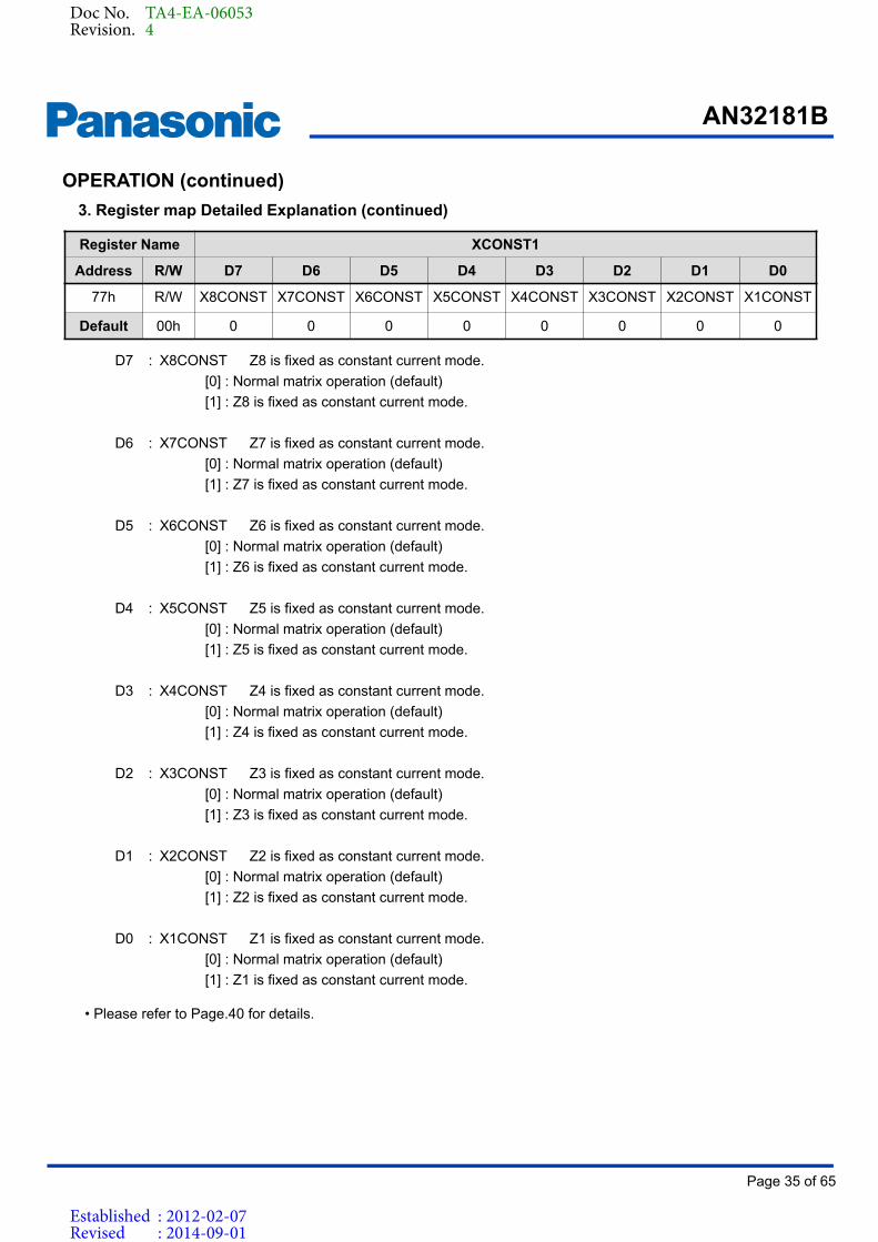
Register Name XCONST1
Address R/W D7 D6 D5 D4 D3 D2 D1 D0
77h R/W X8CONST X7CONST X6CONST X5CONST X4CONST X3CONST X2CONST X1CONST
Default 00h 0 0 0 0 0 0 0 0
D7 : X8CONST Z8 is fixed as constant current mode.
[0] : Normal matrix operation (default)
[1] : Z8 is fixed as constant current mode.
D6 : X7CONST Z7 is fixed as constant current mode.
[0] : Normal matrix operation (default)
[1] : Z7 is fixed as constant current mode.
D5 : X6CONST Z6 is fixed as constant current mode.
[0] : Normal matrix operation (default)
[1] : Z6 is fixed as constant current mode.
D4 : X5CONST Z5 is fixed as constant current mode.
[0] : Normal matrix operation (default)
[1] : Z5 is fixed as constant current mode.
D3 : X4CONST Z4 is fixed as constant current mode.
[0] : Normal matrix operation (default)
[1] : Z4 is fixed as constant current mode.
D2 : X3CONST Z3 is fixed as constant current mode.
[0] : Normal matrix operation (default)
[1] : Z3 is fixed as constant current mode.
D1 : X2CONST Z2 is fixed as constant current mode.
[0] : Normal matrix operation (default)
[1] : Z2 is fixed as constant current mode.
D0 : X1CONST Z1 is fixed as constant current mode.
[0] : Normal matrix operation (default)
[1] : Z1 is fixed as constant current mode.
3. Register map Detailed Explanation (continued)
OPERATION (continued)
• Please refer to Page.40 for details.
Doc No. TA4-EA-06053Revision. 4
Established : 2012-02-07Revised : 2014-09-01
AN32181B
Page 36 of 65
Product Standards
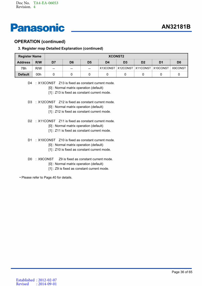
Register Name XCONST2
Address R/W D7 D6 D5 D4 D3 D2 D1 D0
78h R/W -- -- -- X13CONST X12CONST X11CONST X10CONST X9CONST
Default 00h 0 0 0 0 0 0 0 0
D4 : X13CONST Z13 is fixed as constant current mode.
[0] : Normal matrix operation (default)
[1] : Z13 is fixed as constant current mode.
D3 : X12CONST Z12 is fixed as constant current mode.
[0] : Normal matrix operation (default)
[1] : Z12 is fixed as constant current mode.
D2 : X11CONST Z11 is fixed as constant current mode.
[0] : Normal matrix operation (default)
[1] : Z11 is fixed as constant current mode.
D1 : X10CONST Z10 is fixed as constant current mode.
[0] : Normal matrix operation (default)
[1] : Z10 is fixed as constant current mode.
D0 : X9CONST Z9 is fixed as constant current mode.
[0] : Normal matrix operation (default)
[1] : Z9 is fixed as constant current mode.
3. Register map Detailed Explanation (continued)
OPERATION (continued)
• Please refer to Page.40 for details.
Doc No. TA4-EA-06053Revision. 4
Established : 2012-02-07Revised : 2014-09-01
AN32181B
Page 37 of 65
Product Standards
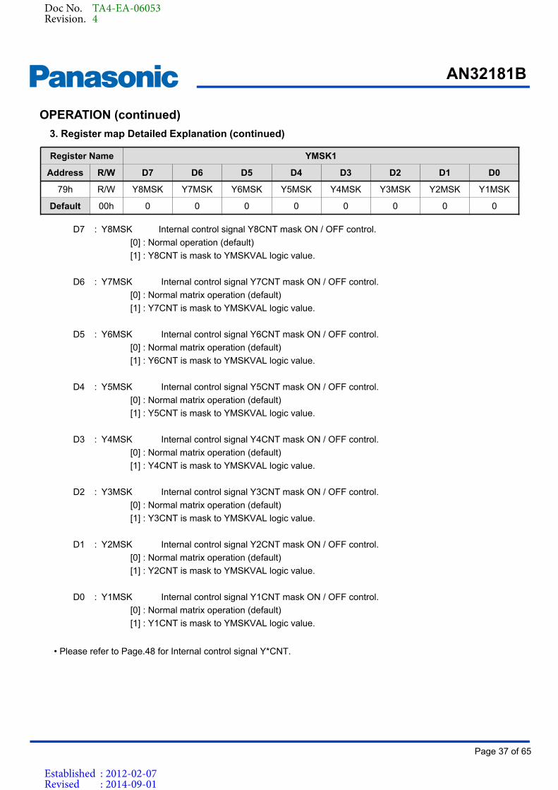
Register Name YMSK1
Address R/W D7 D6 D5 D4 D3 D2 D1 D0
79h R/W Y8MSK Y7MSK Y6MSK Y5MSK Y4MSK Y3MSK Y2MSK Y1MSK
Default 00h 0 0 0 0 0 0 0 0
D7 : Y8MSK Internal control signal Y8CNT mask ON / OFF control.
[0] : Normal operation (default)
[1] : Y8CNT is mask to YMSKVAL logic value.
D6 : Y7MSK Internal control signal Y7CNT mask ON / OFF control.
[0] : Normal matrix operation (default)
[1] : Y7CNT is mask to YMSKVAL logic value.
D5 : Y6MSK Internal control signal Y6CNT mask ON / OFF control.
[0] : Normal matrix operation (default)
[1] : Y6CNT is mask to YMSKVAL logic value.
D4 : Y5MSK Internal control signal Y5CNT mask ON / OFF control.
[0] : Normal matrix operation (default)
[1] : Y5CNT is mask to YMSKVAL logic value.
D3 : Y4MSK Internal control signal Y4CNT mask ON / OFF control.
[0] : Normal matrix operation (default)
[1] : Y4CNT is mask to YMSKVAL logic value.
D2 : Y3MSK Internal control signal Y3CNT mask ON / OFF control.
[0] : Normal matrix operation (default)
[1] : Y3CNT is mask to YMSKVAL logic value.
D1 : Y2MSK Internal control signal Y2CNT mask ON / OFF control.
[0] : Normal matrix operation (default)
[1] : Y2CNT is mask to YMSKVAL logic value.
D0 : Y1MSK Internal control signal Y1CNT mask ON / OFF control.
[0] : Normal matrix operation (default)
[1] : Y1CNT is mask to YMSKVAL logic value.
3. Register map Detailed Explanation (continued)
OPERATION (continued)
• Please refer to Page.48 for Internal control signal Y*CNT.
Doc No. TA4-EA-06053Revision. 4
Established : 2012-02-07Revised : 2014-09-01
AN32181B
Page 38 of 65
Product Standards
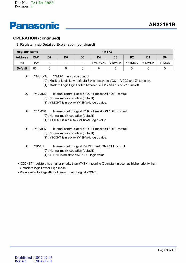
Register Name YMSK2
Address R/W D7 D6 D5 D4 D3 D2 D1 D0
7Ah R/W -- -- -- YMSKVAL Y12MSK Y11MSK Y10MSK Y9MSK
Default 00h 0 0 0 0 0 0 0 0
D4 : YMSKVAL Y*MSK mask value control
[0] : Mask to Logic Low (default) Switch between VCC1 / VCC2 and Z* turns on.
[1] : Mask to Logic High Switch between VCC1 / VCC2 and Z* turns off.
D3 : Y12MSK Internal control signal Y12CNT mask ON / OFF control.
[0] : Normal matrix operation (default)
[1] : Y12CNT is mask to YMSKVAL logic value.
D2 : Y11MSK Internal control signal Y11CNT mask ON / OFF control.
[0] : Normal matrix operation (default)
[1] : Y11CNT is mask to YMSKVAL logic value.
D1 : Y10MSK Internal control signal Y10CNT mask ON / OFF control.
[0] : Normal matrix operation (default)
[1] : Y10CNT is mask to YMSKVAL logic value.
D0 : Y9MSK Internal control signal Y9CNT mask ON / OFF control.
[0] : Normal matrix operation (default)
[1] : Y9CNT is mask to YMSKVAL logic value.
• XCONST* registers has higher priority than YMSK* meaning X constant mode has higher priority than
Y mask to logic Low or High mode.
• Please refer to Page.48 for Internal control signal Y*CNT.
3. Register map Detailed Explanation (continued)
OPERATION (continued)
Doc No. TA4-EA-06053Revision. 4
Established : 2012-02-07Revised : 2014-09-01
AN32181B
Page 39 of 65
Product Standards
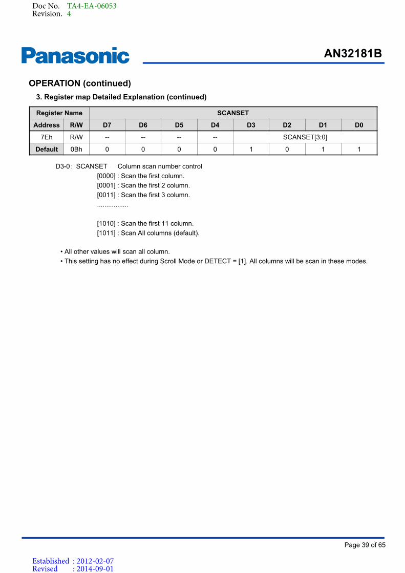
Register Name SCANSET
Address R/W D7 D6 D5 D4 D3 D2 D1 D0
7Eh R/W -- -- -- -- SCANSET[3:0]
Default 0Bh 0 0 0 0 1 0 1 1
D3-0 : SCANSET Column scan number control
[0000] : Scan the first column.
[0001] : Scan the first 2 column.
[0011] : Scan the first 3 column.
.................
[1010] : Scan the first 11 column.
[1011] : Scan All columns (default).
• All other values will scan all column.
• This setting has no effect during Scroll Mode or DETECT = [1]. All columns will be scan in these modes.
3. Register map Detailed Explanation (continued)
OPERATION (continued)
Doc No. TA4-EA-06053Revision. 4
Established : 2012-02-07Revised : 2014-09-01
AN32181B
Page 40 of 65
Product Standards
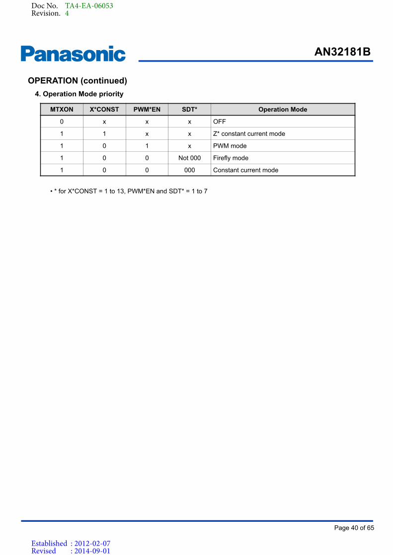
MTXON X*CONST PWM*EN SDT* Operation Mode
0 x x x OFF
1 1 x x Z* constant current mode
1 0 1 x PWM mode
1 0 0 Not 000 Firefly mode
1 0 0 000 Constant current mode
4. Operation Mode priority
OPERATION (continued)
• * for X*CONST = 1 to 13, PWM*EN and SDT* = 1 to 7
Doc No. TA4-EA-06053Revision. 4
Established : 2012-02-07Revised : 2014-09-01
AN32181B
Page 41 of 65
Product Standards
SPI
(SERSEL = High)
I2C
(SERSEL = Low)
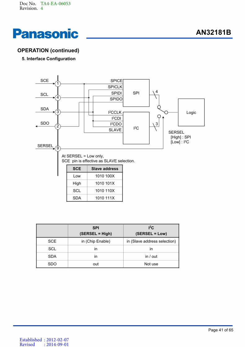
SCE in (Chip Enable) in (Slave address selection)
SCL in in
SDA in in / out
SDO out Not use
SCE Slave address
Low 1010 100X
High 1010 101X
SCL 1010 110X
SDA 1010 111X
SPI
SCE1
SCL4
SDA3
SPICE
SPICLK
SPIDI
SPIDO
I2CCLK
I2CDO
SLAVE
Logic
4
3I2CDI
SDO2 I2C
SERSEL[High] : SPI[Low] : I2C
At SERSEL = Low only,SCE pin is effective as SLAVE selection.
SERSEL9
5. Interface Configuration
OPERATION (continued)
Doc No. TA4-EA-06053Revision. 4
Established : 2012-02-07Revised : 2014-09-01
AN32181B
Page 42 of 65
Product Standards
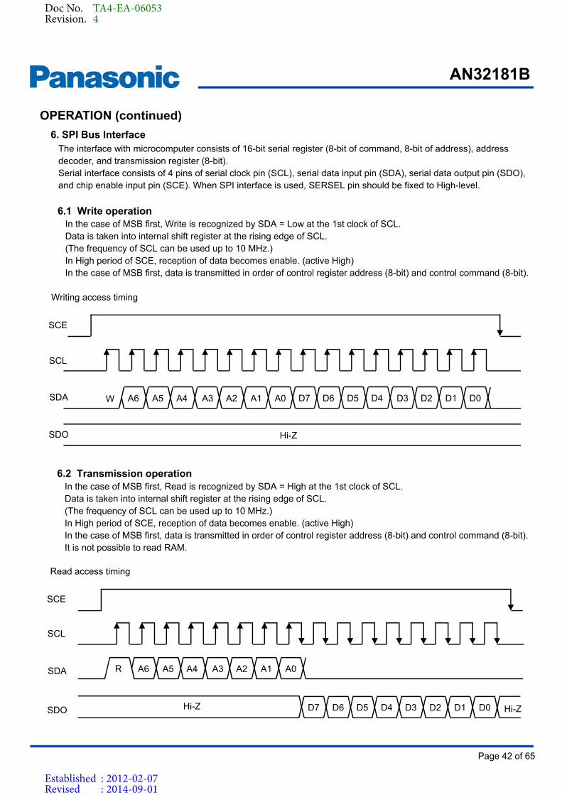
The interface with microcomputer consists of 16-bit serial register (8-bit of command, 8-bit of address), address decoder, and transmission register (8-bit).Serial interface consists of 4 pins of serial clock pin (SCL), serial data input pin (SDA), serial data output pin (SDO), and chip enable input pin (SCE). When SPI interface is used, SERSEL pin should be fixed to High-level.
6.1 Write operationIn the case of MSB first, Write is recognized by SDA = Low at the 1st clock of SCL.Data is taken into internal shift register at the rising edge of SCL.(The frequency of SCL can be used up to 10 MHz.) In High period of SCE, reception of data becomes enable. (active High)In the case of MSB first, data is transmitted in order of control register address (8-bit) and control command (8-bit).
6.2 Transmission operationIn the case of MSB first, Read is recognized by SDA = High at the 1st clock of SCL.Data is taken into internal shift register at the rising edge of SCL.(The frequency of SCL can be used up to 10 MHz.)In High period of SCE, reception of data becomes enable. (active High)In the case of MSB first, data is transmitted in order of control register address (8-bit) and control command (8-bit). It is not possible to read RAM.
SCL
SDA W D0D1D2D3D4D5D6D7A0A1A2A3A4A5A6
SCE
SDO Hi-Z
SCL
SCE
SDA R A0A1A2A3A4A5A6
SDO D0D1D2D3D4D5D6D7Hi-Z Hi-Z
Writing access timing
Read access timing
6. SPI Bus Interface
OPERATION (continued)
Doc No. TA4-EA-06053Revision. 4
Established : 2012-02-07Revised : 2014-09-01
AN32181B
Page 43 of 65
Product Standards
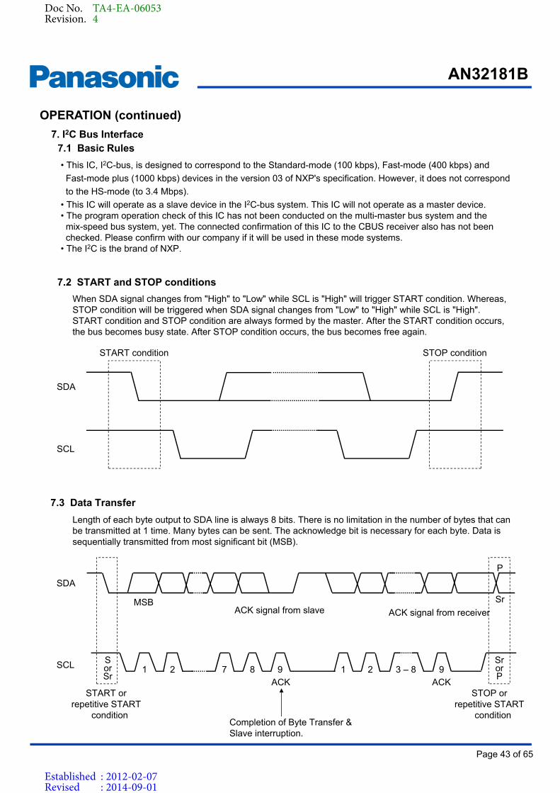
START condition
SDA
SCL
STOP condition
START orrepetitive START
condition
STOP orrepetitive START
condition
SCL
SDA
MSB
ACK ACK1 2 7 8 9 1 2 3 – 8 9
SrorP
Sr
P
SorSr
ACK signal from slave ACK signal from receiver
Completion of Byte Transfer &Slave interruption.
When SDA signal changes from "High" to "Low" while SCL is "High" will trigger START condition. Whereas, STOP condition will be triggered when SDA signal changes from "Low" to "High" while SCL is "High".START condition and STOP condition are always formed by the master. After the START condition occurs, the bus becomes busy state. After STOP condition occurs, the bus becomes free again.
Length of each byte output to SDA line is always 8 bits. There is no limitation in the number of bytes that can be transmitted at 1 time. Many bytes can be sent. The acknowledge bit is necessary for each byte. Data is sequentially transmitted from most significant bit (MSB).
• This IC, I2C-bus, is designed to correspond to the Standard-mode (100 kbps), Fast-mode (400 kbps) and
Fast-mode plus (1000 kbps) devices in the version 03 of NXP's specification. However, it does not correspond
to the HS-mode (to 3.4 Mbps).
• This IC will operate as a slave device in the I2C-bus system. This IC will not operate as a master device.• The program operation check of this IC has not been conducted on the multi-master bus system and the mix-speed bus system, yet. The connected confirmation of this IC to the CBUS receiver also has not been checked. Please confirm with our company if it will be used in these mode systems.
• The I2C is the brand of NXP.
7.1 Basic Rules
7.2 START and STOP conditions
7. I2C Bus Interface
7.3 Data Transfer
OPERATION (continued)
Doc No. TA4-EA-06053Revision. 4
Established : 2012-02-07Revised : 2014-09-01
AN32181B
Page 44 of 65
Product Standards
Data byte can be written in Sub address by transmitting data byte continuously. Sub address is incremented automatically.
S Slave address Sub address
Stop conditionACK : 0
Start condition Write mode : 0
W A A Data byte A P
7-bit 8-bit 8-bit
ACK : 0 ACK : 0
Sub address is not incremented automatically. The next data byte is written in the same Sub address by transmitting data byte continuously.
Sub addressX data
Sub addressX+1 data
S Slave address Sub address
ACK : 0Start condition Write mode : 0
W A A Data byte A
7-bit 8-bit 8-bit
ACK : 0 ACK : 0
Data byte
8-bit
Sub addressX+m-1 data
Sub addressX+m data
Data byte A
8-bit
ACK : 0
Data byte
8-bit
ACK : 0
A P
A
ACK : 0
:Data transmission from Master
:Data transmission from Slave
SCE Slave address
Low 1010 100X
High 1010 101X
SCL 1010 110X
SDA 1010 111X
7.4 I2C Interface - Data Format
In this IC, 4 different Slave address can be changed by selecting SCE ( "Low" or "High" or "SCL" or "SDA"). The slave addresses of this IC are as follow:
Write mode
Write mode (Auto increment mode)
7. I2C Bus Interface (continued)
OPERATION (continued)
Doc No. TA4-EA-06053Revision. 4
Established : 2012-02-07Revised : 2014-09-01
AN32181B
Page 45 of 65
Product Standards
Sub address is not incremented automatically.The next data byte reads the same Sub address by transmitting data byte continuously.
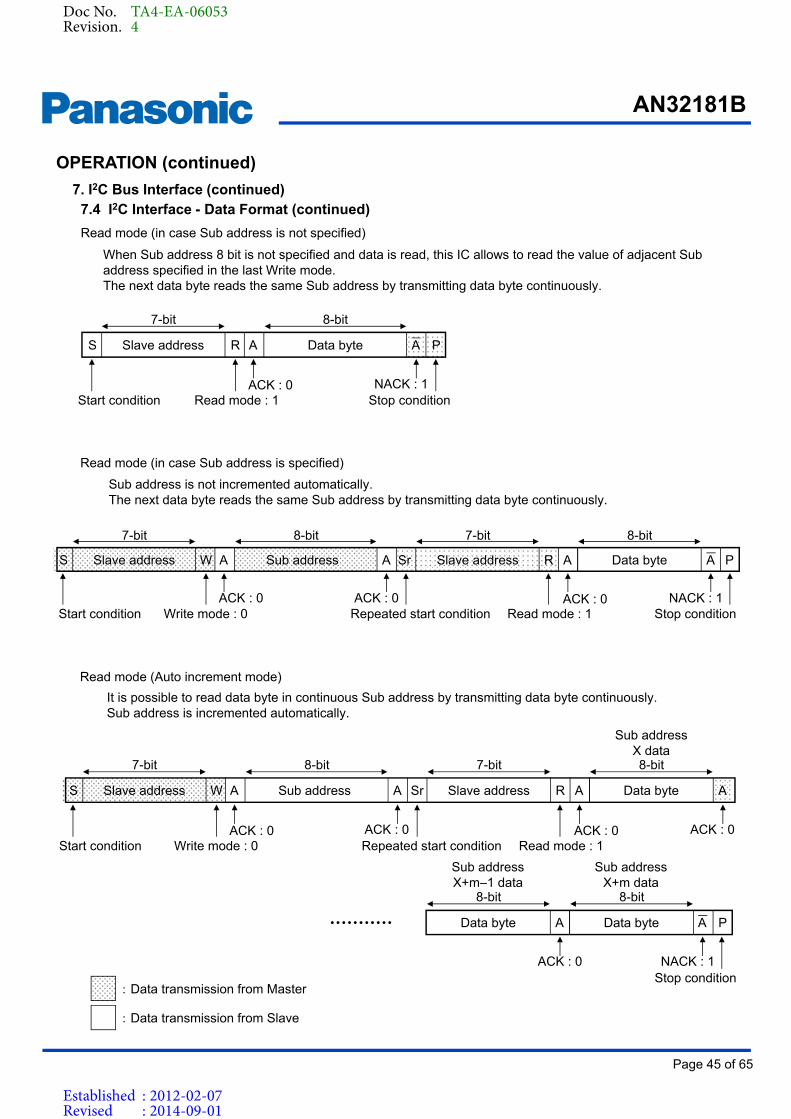
When Sub address 8 bit is not specified and data is read, this IC allows to read the value of adjacent Sub address specified in the last Write mode.The next data byte reads the same Sub address by transmitting data byte continuously.
It is possible to read data byte in continuous Sub address by transmitting data byte continuously. Sub address is incremented automatically.
S Slave address Sub address
ACK : 0Start condition Write mode : 0
W A Sr Slave address A
7-bit 8-bit 7-bit
ACK : 0
Data byte
8-bit
A
NACK : 1
A PR
Stop conditionRepeated start condition Read mode : 1ACK : 0
Sub addressX+m–1 data
Sub addressX+m data
Data byte A
8-bit
ACK : 0
Data byte
8-bit
NACK : 1
A P
S Slave address Sub address
ACK : 0Start condition
W A Sr Slave address A
7-bit 8-bit 7-bit
ACK : 0
Data byte
8-bit
A
ACK : 0
A R
Repeated start condition Read mode : 1ACK : 0
Sub addressX data
Stop condition
Write mode : 0
S Slave address Data byte
Stop conditionACK : 0
Start condition Read mode : 1
R A A P
7-bit 8-bit
NACK : 1
7.4 I2C Interface - Data Format (continued)
Read mode (in case Sub address is not specified)
Read mode (in case Sub address is specified)
Read mode (Auto increment mode)
7. I2C Bus Interface (continued)
:Data transmission from Master
:Data transmission from Slave
OPERATION (continued)
Doc No. TA4-EA-06053Revision. 4
Established : 2012-02-07Revised : 2014-09-01
AN32181B
Page 46 of 65
Product Standards
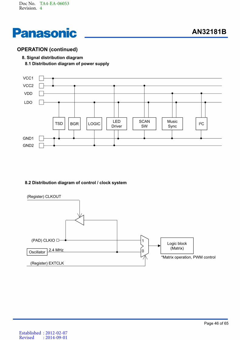
8.2 Distribution diagram of control / clock system
Oscillator 2.4 MHz
(PAD) CLKIO
(Register) EXTCLK
Logic block(Matrix)
*Matrix operation, PWM control
1
0
(Register) CLKOUT
8.1 Distribution diagram of power supply8. Signal distribution diagram
OPERATION (continued)
VCC2
LDO
VDD
GND1
GND2
LOGICSCAN
SWI2CBGR
LEDDriver
MusicSync
TSD
VCC1
Doc No. TA4-EA-06053Revision. 4
Established : 2012-02-07Revised : 2014-09-01
AN32181B
Page 47 of 65
Product Standards
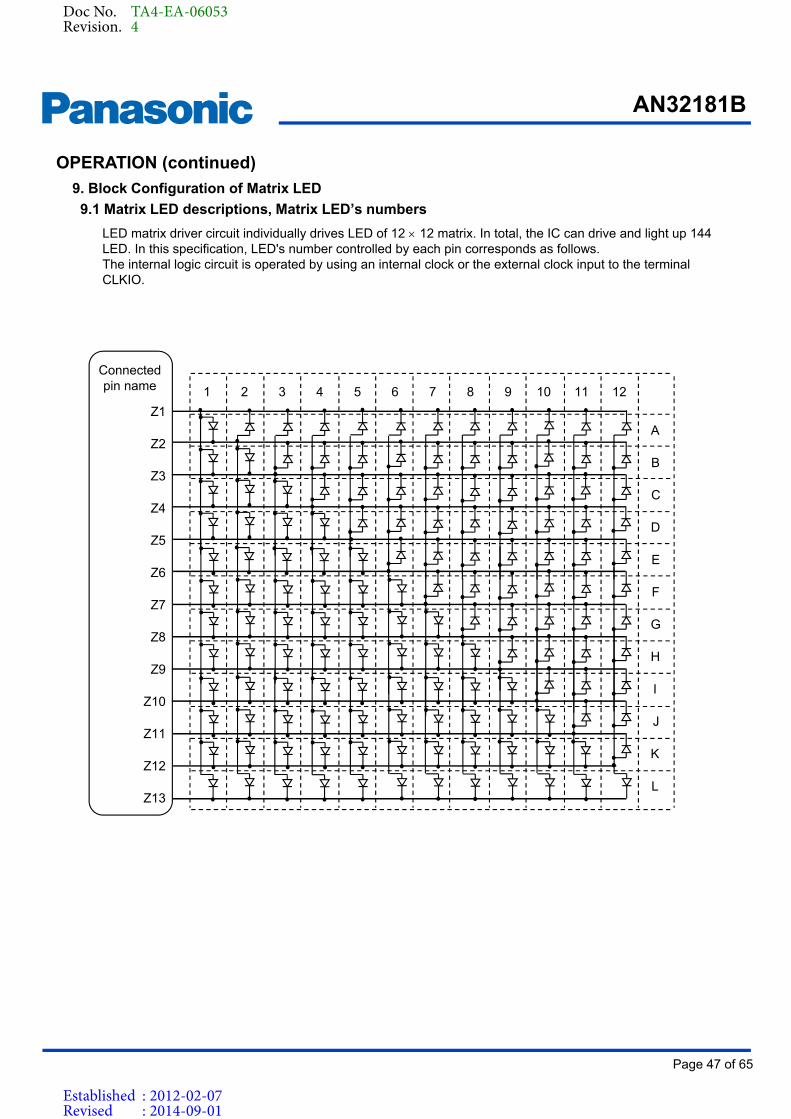
LED matrix driver circuit individually drives LED of 12 12 matrix. In total, the IC can drive and light up 144 LED. In this specification, LED's number controlled by each pin corresponds as follows.The internal logic circuit is operated by using an internal clock or the external clock input to the terminal CLKIO.
9. Block Configuration of Matrix LED
9.1 Matrix LED descriptions, Matrix LED’s numbers
OPERATION (continued)
Connectedpin name
Z4
Z3
Z5
Z1
Z2
Z9
Z8
Z10
Z6
Z7
Z12
Z11
Z13
4321
D
C
B
A
8765 1211109
H
G
F
E
L
K
J
I
Doc No. TA4-EA-06053Revision. 4
Established : 2012-02-07Revised : 2014-09-01
AN32181B
Page 48 of 65
Product Standards
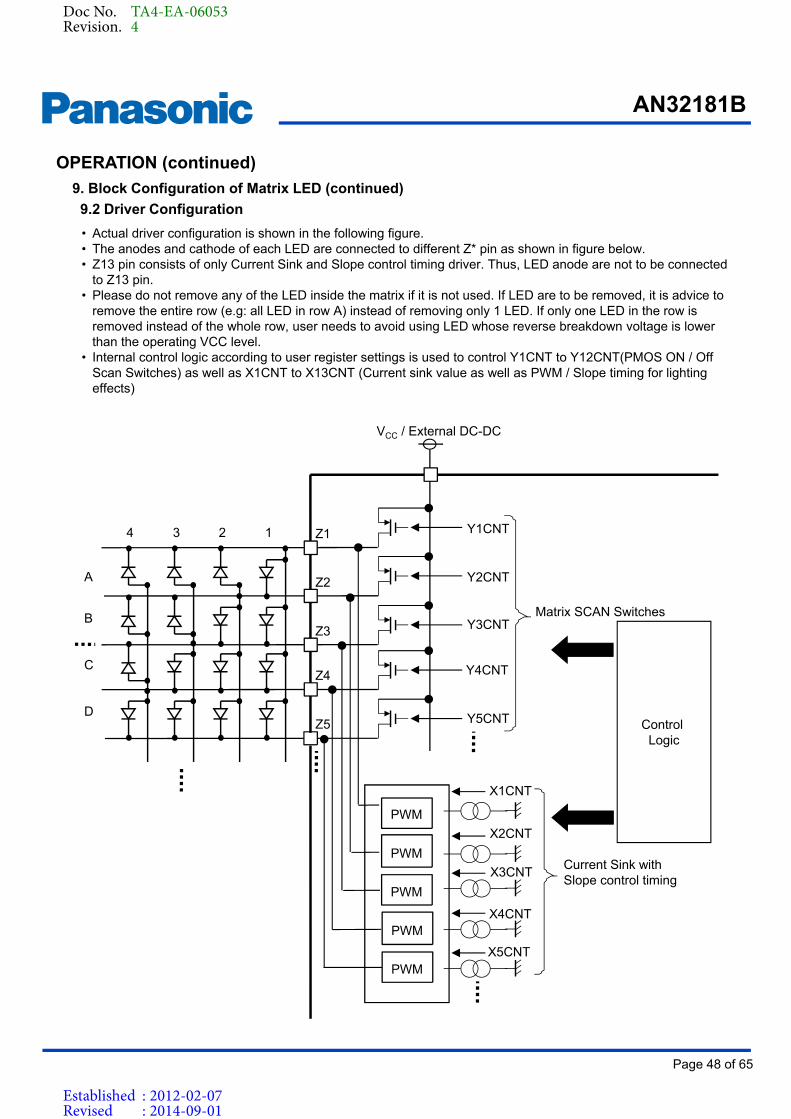
• Actual driver configuration is shown in the following figure.• The anodes and cathode of each LED are connected to different Z* pin as shown in figure below. • Z13 pin consists of only Current Sink and Slope control timing driver. Thus, LED anode are not to be connected
to Z13 pin.• Please do not remove any of the LED inside the matrix if it is not used. If LED are to be removed, it is advice to
remove the entire row (e.g: all LED in row A) instead of removing only 1 LED. If only one LED in the row is removed instead of the whole row, user needs to avoid using LED whose reverse breakdown voltage is lower than the operating VCC level.
• Internal control logic according to user register settings is used to control Y1CNT to Y12CNT(PMOS ON / Off Scan Switches) as well as X1CNT to X13CNT (Current sink value as well as PWM / Slope timing for lighting effects)
VCC / External DC-DC
PWM
PWM
PWM
Y3CNT
Y4CNT
Y2CNT
Y1CNT
PWM
PWM
X2CNT
X4CNT
X3CNT
X5CNT
Matrix SCAN Switches
Current Sink with Slope control timing
Control Logic
Y5CNT
X1CNT
1234
A
B
C
D
9. Block Configuration of Matrix LED (continued)
9.2 Driver Configuration
OPERATION (continued)
Z5
Z4
Z3
Z2
Z1
Doc No. TA4-EA-06053Revision. 4
Established : 2012-02-07Revised : 2014-09-01
AN32181B
Page 49 of 65
Product Standards
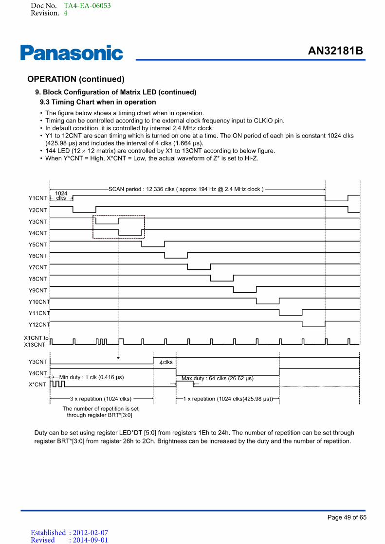
9.3 Timing Chart when in operation
Duty can be set using register LED*DT [5:0] from registers 1Eh to 24h. The number of repetition can be set through register BRT*[3:0] from register 26h to 2Ch. Brightness can be increased by the duty and the number of repetition.
• The figure below shows a timing chart when in operation.• Timing can be controlled according to the external clock frequency input to CLKIO pin.• In default condition, it is controlled by internal 2.4 MHz clock.• Y1 to 12CNT are scan timing which is turned on one at a time. The ON period of each pin is constant 1024 clks
(425.98 µs) and includes the interval of 4 clks (1.664 µs).• 144 LED (12 12 matrix) are controlled by X1 to 13CNT according to below figure.• When Y*CNT = High, X*CNT = Low, the actual waveform of Z* is set to Hi-Z.
9. Block Configuration of Matrix LED (continued)
Y1CNT
Y2CNT
Y3CNT
Y4CNT
Y5CNT
Y6CNT
Y7CNT
Y8CNT
Y9CNT
Y10CNT
Y11CNT
Y12CNT
1024clks
4
Max duty : 64 clks (26.62 µs)
3 x repetition (1024 clks)
The number of repetition is set through register BRT*[3:0]
X*CNT
Y3CNT
Y4CNTMin duty : 1 clk (0.416 µs)
clks
1 x repetition (1024 clks(425.98 µs))
X1CNT toX13CNT
SCAN period : 12,336 clks ( approx 194 Hz @ 2.4 MHz clock )
OPERATION (continued)
Doc No. TA4-EA-06053Revision. 4
Established : 2012-02-07Revised : 2014-09-01
AN32181B
Page 50 of 65
Product Standards
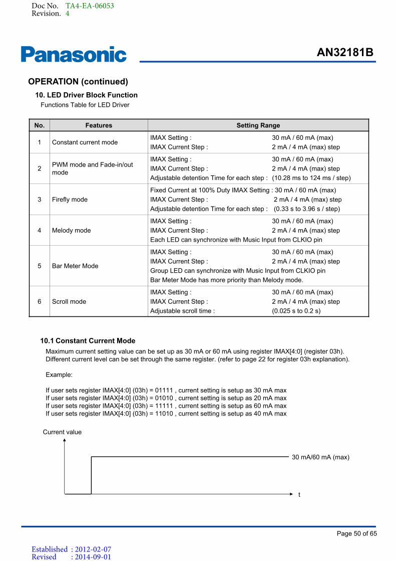
10.1 Constant Current Mode
No. Features Setting Range
1 Constant current modeIMAX Setting : 30 mA / 60 mA (max)
IMAX Current Step : 2 mA / 4 mA (max) step
2PWM mode and Fade-in/out mode
IMAX Setting : 30 mA / 60 mA (max)
IMAX Current Step : 2 mA / 4 mA (max) step
Adjustable detention Time for each step : (10.28 ms to 124 ms / step)
3 Firefly mode
Fixed Current at 100% Duty IMAX Setting : 30 mA / 60 mA (max)
IMAX Current Step : 2 mA / 4 mA (max) step
Adjustable detention Time for each step : (0.33 s to 3.96 s / step)
4 Melody mode
IMAX Setting : 30 mA / 60 mA (max)
IMAX Current Step : 2 mA / 4 mA (max) step
Each LED can synchronize with Music Input from CLKIO pin
5 Bar Meter Mode
IMAX Setting : 30 mA / 60 mA (max)
IMAX Current Step : 2 mA / 4 mA (max) step
Group LED can synchronize with Music Input from CLKIO pin
Bar Meter Mode has more priority than Melody mode.
6 Scroll mode
IMAX Setting : 30 mA / 60 mA (max)
IMAX Current Step : 2 mA / 4 mA (max) step
Adjustable scroll time : (0.025 s to 0.2 s)
30 mA/60 mA (max)
t
Current value
Functions Table for LED Driver
Maximum current setting value can be set up as 30 mA or 60 mA using register IMAX[4:0] (register 03h). Different current level can be set through the same register. (refer to page 22 for register 03h explanation).
Example:
If user sets register IMAX[4:0] (03h) = 01111 , current setting is setup as 30 mA maxIf user sets register IMAX[4:0] (03h) = 01010 , current setting is setup as 20 mA maxIf user sets register IMAX[4:0] (03h) = 11111 , current setting is setup as 60 mA maxIf user sets register IMAX[4:0] (03h) = 11010 , current setting is setup as 40 mA max
10. LED Driver Block Function
OPERATION (continued)
Doc No. TA4-EA-06053Revision. 4
Established : 2012-02-07Revised : 2014-09-01
AN32181B
Page 51 of 65
Product Standards
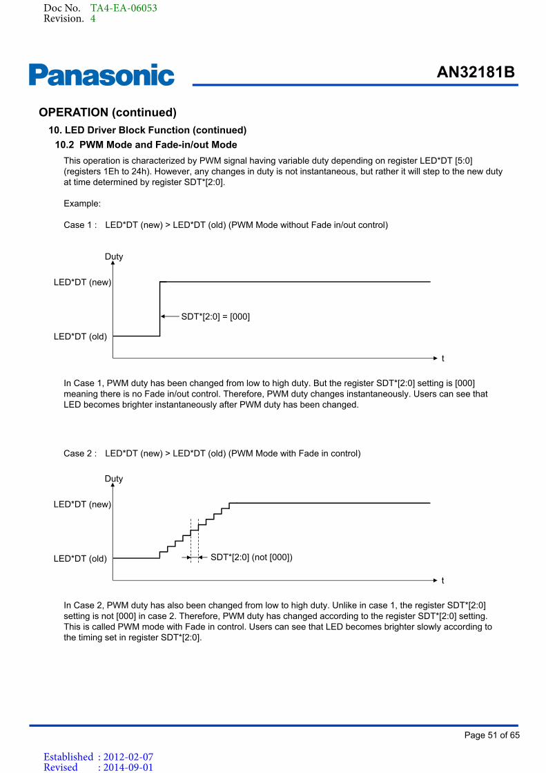
Case 2 : LED*DT (new) > LED*DT (old) (PWM Mode with Fade in control)
In Case 1, PWM duty has been changed from low to high duty. But the register SDT*[2:0] setting is [000] meaning there is no Fade in/out control. Therefore, PWM duty changes instantaneously. Users can see that LED becomes brighter instantaneously after PWM duty has been changed.
In Case 2, PWM duty has also been changed from low to high duty. Unlike in case 1, the register SDT*[2:0] setting is not [000] in case 2. Therefore, PWM duty has changed according to the register SDT*[2:0] setting. This is called PWM mode with Fade in control. Users can see that LED becomes brighter slowly according to the timing set in register SDT*[2:0].
t
SDT*[2:0] = [000]
LED*DT (new)
LED*DT (old)
Duty
t
SDT*[2:0] (not [000])
LED*DT (new)
LED*DT (old)
Duty
This operation is characterized by PWM signal having variable duty depending on register LED*DT [5:0] (registers 1Eh to 24h). However, any changes in duty is not instantaneous, but rather it will step to the new duty at time determined by register SDT*[2:0].
Example:
Case 1 : LED*DT (new) > LED*DT (old) (PWM Mode without Fade in/out control)
10. LED Driver Block Function (continued)
10.2 PWM Mode and Fade-in/out Mode
OPERATION (continued)
Doc No. TA4-EA-06053Revision. 4
Established : 2012-02-07Revised : 2014-09-01
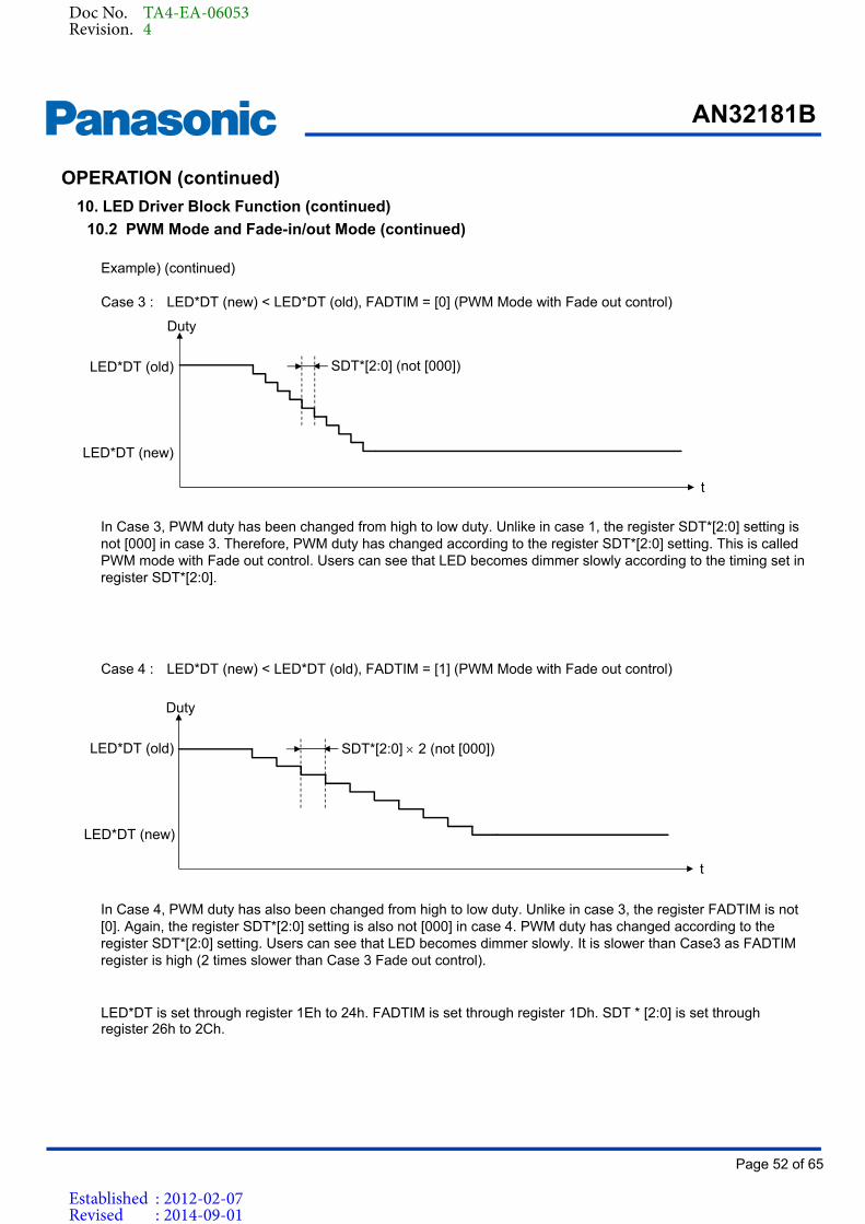
AN32181B
Page 52 of 65
Product Standards
LED*DT is set through register 1Eh to 24h. FADTIM is set through register 1Dh. SDT * [2:0] is set through register 26h to 2Ch.
Example) (continued)
Case 3 : LED*DT (new) < LED*DT (old), FADTIM = [0] (PWM Mode with Fade out control)
t
SDT*[2:0] (not [000])LED*DT (old)
LED*DT (new)
Duty
In Case 3, PWM duty has been changed from high to low duty. Unlike in case 1, the register SDT*[2:0] setting is not [000] in case 3. Therefore, PWM duty has changed according to the register SDT*[2:0] setting. This is called PWM mode with Fade out control. Users can see that LED becomes dimmer slowly according to the timing set in register SDT*[2:0].
Case 4 : LED*DT (new) < LED*DT (old), FADTIM = [1] (PWM Mode with Fade out control)
t
SDT*[2:0] 2 (not [000])LED*DT (old)
LED*DT (new)
Duty
In Case 4, PWM duty has also been changed from high to low duty. Unlike in case 3, the register FADTIM is not [0]. Again, the register SDT*[2:0] setting is also not [000] in case 4. PWM duty has changed according to the register SDT*[2:0] setting. Users can see that LED becomes dimmer slowly. It is slower than Case3 as FADTIM register is high (2 times slower than Case 3 Fade out control).
10. LED Driver Block Function (continued)
10.2 PWM Mode and Fade-in/out Mode (continued)
OPERATION (continued)
Doc No. TA4-EA-06053Revision. 4
Established : 2012-02-07Revised : 2014-09-01
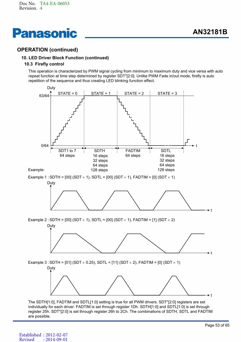
AN32181B
Page 53 of 65
Product Standards
Example:
Example 1 : SDTH = [00] (SDT 1), SDTL = [00] (SDT 1), FADTIM = [0] (SDT 1)
Example 2 : SDTH = [00] (SDT 1), SDTL = [00] (SDT 1), FADTIM = [1] (SDT 2)
Example 3 : SDTH = [01] (SDT 0.25), SDTL = [11] (SDT 2), FADTIM = [0] (SDT 1)
t
Duty
t
Duty
The SDTH[1:0], FADTIM and SDTL[1:0] setting is true for all PWM drivers. SDT*[2:0] registers are set individually for each driver. FADTIM is set through register 1Dh. SDTH[1:0] and SDTL[1:0] is set through register 25h. SDT*[2:0] is set through register 26h to 2Ch. The combinations of SDTH, SDTL and FADTIM are possible.
t
Duty
t
63/64
Duty
0/64
STATE = 0 STATE = 1 STATE = 2 STATE = 3
SDT1 to 764 steps
SDTH FADTIM64 steps
SDTL
This operation is characterized by PWM signal cycling from minimum to maximum duty and vice versa with auto repeat function at time step determined by register SDT*[2:0]. Unlike PWM Fade in/out mode, firefly is auto repetition of the sequence and thus creating LED blinking function effect.
10. LED Driver Block Function (continued)
10.3 Firefly control
OPERATION (continued)
16 steps32 steps64 steps
128 steps
16 steps32 steps64 steps
128 steps
Doc No. TA4-EA-06053Revision. 4
Established : 2012-02-07Revised : 2014-09-01
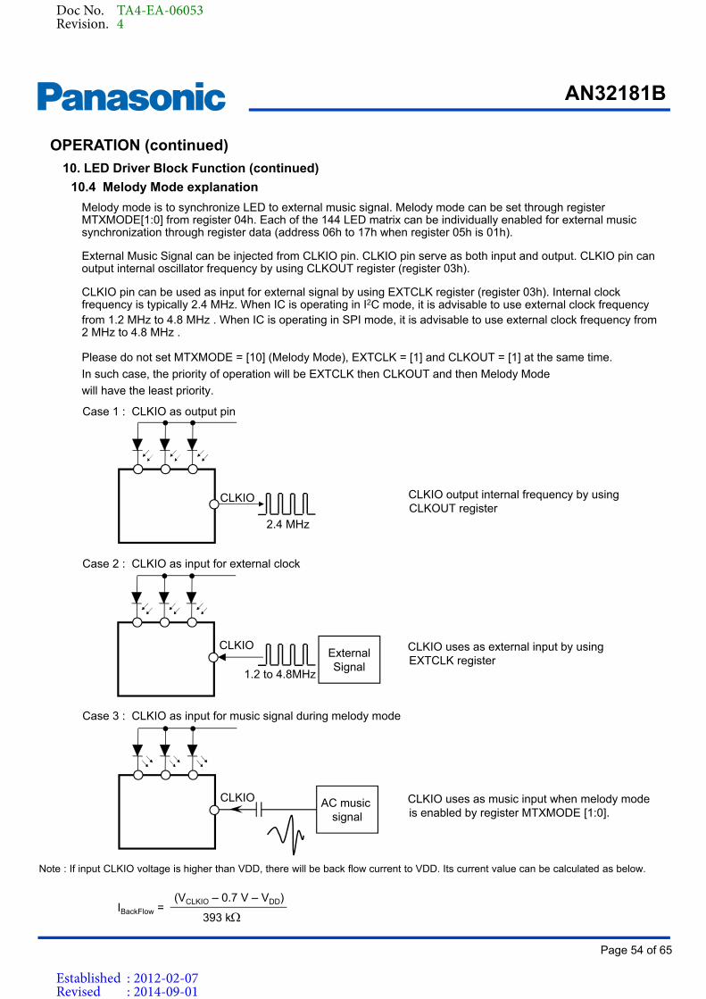
AN32181B
Page 54 of 65
Product Standards
Case 1 : CLKIO as output pin
CLKIO output internal frequency by using CLKOUT register
Case 2 : CLKIO as input for external clock
CLKIO uses as external input by using EXTCLK register
Case 3 : CLKIO as input for music signal during melody mode
CLKIO uses as music input when melody mode is enabled by register MTXMODE [1:0].
Melody mode is to synchronize LED to external music signal. Melody mode can be set through register MTXMODE[1:0] from register 04h. Each of the 144 LED matrix can be individually enabled for external music synchronization through register data (address 06h to 17h when register 05h is 01h).
External Music Signal can be injected from CLKIO pin. CLKIO pin serve as both input and output. CLKIO pin can output internal oscillator frequency by using CLKOUT register (register 03h).
CLKIO pin can be used as input for external signal by using EXTCLK register (register 03h). Internal clock frequency is typically 2.4 MHz. When IC is operating in I2C mode, it is advisable to use external clock frequency from 1.2 MHz to 4.8 MHz . When IC is operating in SPI mode, it is advisable to use external clock frequency from 2 MHz to 4.8 MHz .
Please do not set MTXMODE = [10] (Melody Mode), EXTCLK = [1] and CLKOUT = [1] at the same time.
In such case, the priority of operation will be EXTCLK then CLKOUT and then Melody Mode
will have the least priority.
CLKIO
2.4 MHz
External Signal
1.2 to 4.8MHz
CLKIO
AC music signal
CLKIO
Note : If input CLKIO voltage is higher than VDD, there will be back flow current to VDD. Its current value can be calculated as below.
IBackFlow =
10. LED Driver Block Function (continued)
10.4 Melody Mode explanation
OPERATION (continued)
(VCLKIO – 0.7 V – VDD)
393 k
Doc No. TA4-EA-06053Revision. 4
Established : 2012-02-07Revised : 2014-09-01
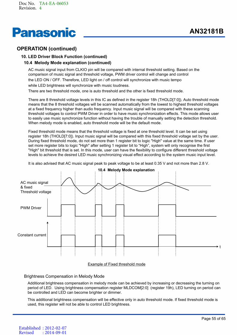
AN32181B
Page 55 of 65
Product Standards
AC music signal input from CLKIO pin will be compared with internal threshold setting. Based on the comparison of music signal and threshold voltage, PWM driver control will change and control
the LED ON / OFF. Therefore, LED light on / off control will synchronize with music tempo
while LED brightness will synchronize with music loudness.
There are two threshold mode, one is auto threshold and the other is fixed threshold mode.
There are 8 threshold voltage levels in this IC as defined in the register 18h (THOLD[7:0]). Auto threshold mode means that the 8 threshold voltages will be scanned automatically from the lowest to highest threshold voltages at a fixed frequency higher than audio frequency. Input music signal will be compared with these scanning threshold voltages to control PWM Driver in order to have music synchronization effects. This mode allows user to easily use music synchronize function without having the trouble of manually setting the detection threshold. When melody mode is enabled, auto threshold mode will be the default mode.
Fixed threshold mode means that the threshold voltage is fixed at one threshold level. It can be set using register 18h (THOLD[7:0]). Input music signal will be compared with this fixed threshold voltage set by the user. During fixed threshold mode, do not set more than 1 register bit to logic "High" value at the same time. If user set more register bits to logic "High" after setting 1 register bit to “High”, system will only recognise the first "High" bit threshold that is set. In this mode, user can have the flexibility to configure different threshold voltage levels to achieve the desired LED music synchronizing visual effect according to the system music input level.
It is also advised that AC music signal peak to peak voltage to be at least 0.35 V and not more than 2.8 V.
Example of Fixed threshold mode
Additional brightness compensation in melody mode can be achieved by increasing or decreasing the turning on period of LED. Using brightness compensation register MLDCOM[2:0] (register 19h), LED turning on period can be controlled and LED can become brighter or dimmer.
This additional brightness compensation will be effective only in auto threshold mode. If fixed threshold mode is used, this register will not be able to control LED brightness.
PWM Driver
Constant current
AC music signal& fixed Threshold voltage
t
Brightness Compensation in Melody Mode
10.4 Melody Mode explanation
10. LED Driver Block Function (continued)
10.4 Melody Mode explanation (continued)
OPERATION (continued)
Doc No. TA4-EA-06053Revision. 4
Established : 2012-02-07Revised : 2014-09-01
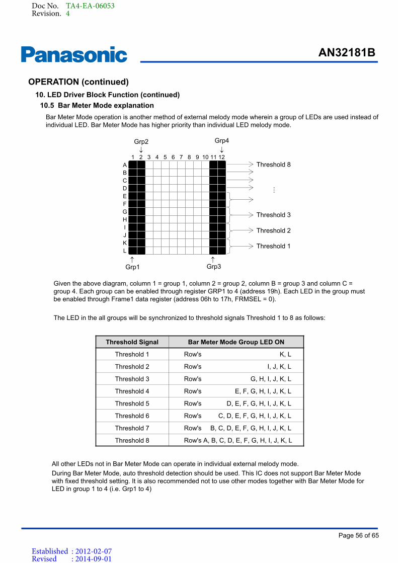
AN32181B
Page 56 of 65
Product Standards
Given the above diagram, column 1 = group 1, column 2 = group 2, column B = group 3 and column C = group 4. Each group can be enabled through register GRP1 to 4 (address 19h). Each LED in the group must be enabled through Frame1 data register (address 06h to 17h, FRMSEL = 0).
The LED in the all groups will be synchronized to threshold signals Threshold 1 to 8 as follows:
All other LEDs not in Bar Meter Mode can operate in individual external melody mode.
During Bar Meter Mode, auto threshold detection should be used. This IC does not support Bar Meter Mode with fixed threshold setting. It is also recommended not to use other modes together with Bar Meter Mode for LED in group 1 to 4 (i.e. Grp1 to 4)
Threshold Signal Bar Meter Mode Group LED ON
Threshold 1 Row's K, L
Threshold 2 Row's I, J, K, L
Threshold 3 Row's G, H, I, J, K, L
Threshold 4 Row's E, F, G, H, I, J, K, L
Threshold 5 Row's D, E, F, G, H, I, J, K, L
Threshold 6 Row's C, D, E, F, G, H, I, J, K, L
Threshold 7 Row's B, C, D, E, F, G, H, I, J, K, L
Threshold 8 Row's A, B, C, D, E, F, G, H, I, J, K, L
Bar Meter Mode operation is another method of external melody mode wherein a group of LEDs are used instead of individual LED. Bar Meter Mode has higher priority than individual LED melody mode.
1 2 3 4 5 6 7 8 9 10 11 12ABCDEFGHIJKL
Grp1
Grp2
Grp3
Grp4
Threshold 1
…
Threshold 2
Threshold 3
Threshold 8
10. LED Driver Block Function (continued)
10.5 Bar Meter Mode explanation
OPERATION (continued)
Doc No. TA4-EA-06053Revision. 4
Established : 2012-02-07Revised : 2014-09-01

AN32181B
Page 57 of 65
Product Standards
Frame1 Frame2
(A) (B) (C) (N)
INT
SCLTIME 12
1 2 3 4 5
10. LED Driver Block Function (continued)
10.6 Scroll Mode explanation
Example:
Example 1 : From right to left
Scroll Mode can be set through MTXMODE [1:0] register (register 04h). The specified character can be scrolledfor display from right to left or bottom to up using register LEFT or UP (register 75h).If both LEFT and UPregisters are set [1], LEFT will have higher priority. Interrupt signal will be generated every time a full framehas been shifted and it will reflect at interrupt (INT) pin. Interrupt register (register 1Bh) should be unmasked.INT pin is an open drain connection and needs to be pulled up to VDD level.
The scroll time (SCLTIME) can be controlled by the setting of 76h register. The scroll time means the time thatthe display changes the (A) state to the (B) state, (B) to (C) state and so on (the display shifts one column) inthe following figure (ex. LEFT scroll setting). In this IC, there are 12 columns in matrix display. Therefore, itneeds 12 x SCLTIME timing to shift all the columns from Frame1 to Frame2 or vice versa. The initial defaultsetting of scroll time is 0.025 s.
The below example shows how Frame1 and Frame2 data is scroll LEFT. First, User has to write data intoFrame1 and Frame2. At the start of scroll operation, Frame1 is displayed (A). Interrupt will generate and INT pinwill go low (at 1). User can write another data to Frame1 at that time. The data has to be written within12 x SCLTIME timing (12 x 0.025sec for default) during the frame shifting. Once user finishes writing the datainto Frame1, interrupt will clear and INT pin will go high (at 2). Scroll function will operate at the same timingof writing. For scrolling LEFT, the displayed data is shifted one position left and the right-most column is shiftedwith Frame2 column. This continues until the full Frame2 data is shifted in (N). Interrupt will generate againafter Frame2 data is shifted in and INT pin will go low (at 3). User can now write another data to Frame2.The scrolling function will continue to display the new data from the Frame1. Once user finishes writing the datainto Frame2, interrupt will clear and INT pin will go high again (at 4). During this writing, the display willcontinue shifting until new data of Frame 1 is shifted in. After all the new data of Frame1 is shifted in, interruptwill generate and INT pin will go low (at 5). If user does not write any data, INT will still low and scrolling functionwill repeat between the data of Frame1 and Frame 2 until Matrix and scroll mode is turned OFF. The sameoperation is also true for Scroll UP. The difference is that the displayed data is shifted one position up and the1st row of Frame 2 is shifted at the bottom of the display.
OPERATION (continued)
Doc No. TA4-EA-06053Revision. 4
Established : 2012-02-07Revised : 2014-09-01

AN32181B
Page 58 of 65
Product Standards
The stop function allows row A to E to be stationary during scroll mode (can be set using register 75h). The shifting of stop row is done in one bulk at the end of each full frame. Row A to E stop function has individual controls hence combination of rows to stop is possible. Stop function is only valid if the direction selected is scroll LEFT. It has no effect if scroll direction is UP.
If stop register settings (register 75h) is changed during scroll operation, it will only take effect once the full frame has been shifted in. This prevents the character from mis-aligning. The same behavior is also true for direction registers UP and LEFT (register 75h).
10. LED Driver Block Function (continued)
10.6 Scroll Mode explanation (continued)
Example: (continued)
Example 2 : Stop function
Scroll lower rows but Row A to E are stationary After full frame 2 is shifted, Row A to E is updated
RowA to E
RowA to E
Frame1 Frame2
OPERATION (continued)
Doc No. TA4-EA-06053Revision. 4
Established : 2012-02-07Revised : 2014-09-01
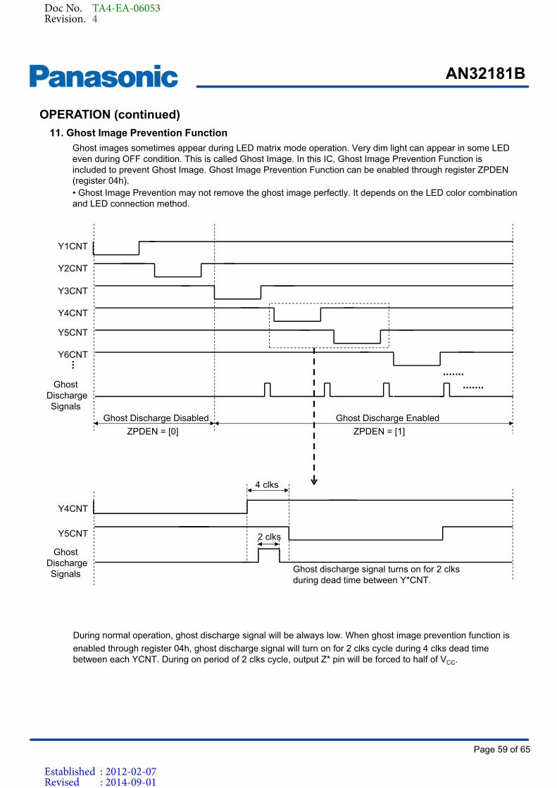
AN32181B
Page 59 of 65
Product Standards
Ghost images sometimes appear during LED matrix mode operation. Very dim light can appear in some LED even during OFF condition. This is called Ghost Image. In this IC, Ghost Image Prevention Function is included to prevent Ghost Image. Ghost Image Prevention Function can be enabled through register ZPDEN (register 04h).• Ghost Image Prevention may not remove the ghost image perfectly. It depends on the LED color combination and LED connection method.
During normal operation, ghost discharge signal will be always low. When ghost image prevention function is
enabled through register 04h, ghost discharge signal will turn on for 2 clks cycle during 4 clks dead time between each YCNT. During on period of 2 clks cycle, output Z* pin will be forced to half of VCC.
11. Ghost Image Prevention Function
Ghost DischargeSignals
Ghost Discharge Disabled Ghost Discharge Enabled
Ghost discharge signal turns on for 2 clks during dead time between Y*CNT.
OPERATION (continued)
Y1CNT
Y2CNT
Y3CNT
Y4CNT
4 clks
Y4CNT
Y5CNT
Y5CNT
Y6CNT
2 clks
ZPDEN = [0] ZPDEN = [1]
Ghost DischargeSignals
Doc No. TA4-EA-06053Revision. 4
Established : 2012-02-07Revised : 2014-09-01
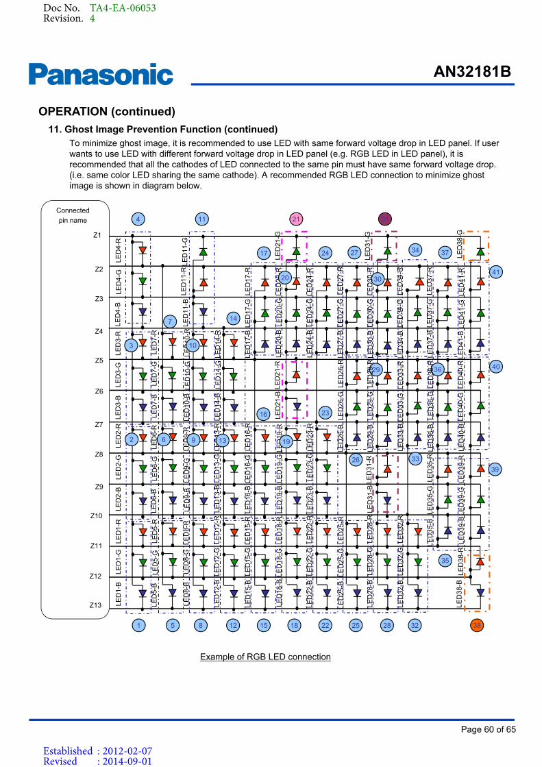
AN32181B
Page 60 of 65
Product Standards
11. Ghost Image Prevention Function (continued)
OPERATION (continued)
To minimize ghost image, it is recommended to use LED with same forward voltage drop in LED panel. If user wants to use LED with different forward voltage drop in LED panel (e.g. RGB LED in LED panel), it is recommended that all the cathodes of LED connected to the same pin must have same forward voltage drop. (i.e. same color LED sharing the same cathode). A recommended RGB LED connection to minimize ghost image is shown in diagram below.
Example of RGB LED connection
LED
1-B
LED
1-G
LED
1-R
LED
2-R
LED
2-G
LED
2-B
LED
3-B
LED
3-R
LED
3-G
LED
5-R
LED
5-B
LED
5-G
LED
4-R
LED
4-B
LED
4-G
LED
6-R
LED
6-B
LED
6-G
LED
7-R
LED
7-B
LED
7-G
LED
10-R
LED
10-B
LED
10-G
LED
9-R
LED
9-G
LED
8-B
LED
8-R
LED
8-G
LED
11-R
LED
11-B
LED
11-G
LED
13-R
LED
13-B
LED
13-G
LED
14-R
LED
14-B
LED
14-G
LED
15-R
LED
15-G
LED
15-B
LED
16-R
LED
16-B
LED
16-G
LED
18-R
LED
18-B
LED
18-G
LED
21-R
LED
21-B
LED
21-G
LED
22-R
LED
22-B
LED
22-G
LED
19-R
LED
19-B
LED
19-G
LED
17-R
LED
17-G
LED
17-B
LED
20-R
LED
20-B
LED
20-G
LED
9-B
Connected
pin name
Z4
Z3
Z5
Z1
Z2
Z9
Z8
Z10
Z6
Z7
Z12
Z11
Z13
1
2
3
4
85
6
7
10
12
11
9
23
38
13
21
19
17
16
14
18 2215
20
24
25
26
27
28
29
30
31
32
33
34
35
36
37
39
40
41
LED
12-R
LED
12-B
LED
12-G
LED
41-R
LED
41-B
LED
41-G
LED
23-R
LED
23-B
LED
23-G
LED
24-R
LED
24-B
LED
24-G
LED
25-R
LED
25-B
LED
25-G
LED
26-R
LED
26-B
LED
26-G
LED
27-R
LED
27-B
LED
27-G
LED
28-R
LED
28-B
LED
28-G
LED
29-R
LED
29-B
LED
29-G
LED
30-R
LED
30-B
LED
30-G
LED
31-R
LED
31-B
LED
31-G
LED
32-R
LED
32-B
LED
32-G
LED
33-R
LED
33-B
LED
33-G
LED
34-R
LED
34-B
LED
34-G
LED
35-R
LED
35-B
LED
35-G
LED
36-R
LED
36-B
LED
36-G
LED
37-R
LED
37-B
LED
37-G
LED
38-R
LED
38-B
LED
38-G
LED
39-R
LED
39-B
LED
39-G
LED
40-R
LED
40-B
LED
40-G
Doc No. TA4-EA-06053Revision. 4
Established : 2012-02-07Revised : 2014-09-01
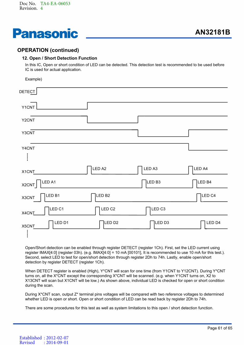
AN32181B
Page 61 of 65
Product Standards
In this IC, Open or short condition of LED can be detected. This detection test is recommended to be used before IC is used for actual application.
Example)
Open/Short detection can be enabled through register DETECT (register 1Ch). First, set the LED current using register IMAX[4:0] (register 03h). (e.g. IMAX[4:0] = 10 mA [00101], It is recommended to use 10 mA for this test.). Second, select LED to test for open/short detection through register 2Dh to 74h. Lastly, enable open/short detection by register DETECT (register 1Ch).
When DETECT register is enabled (High), Y*CNT will scan for one time (from Y1CNT to Y12CNT). During Y*CNT turns on, all the X*CNT except the corresponding X*CNT will be scanned. (e.g. when Y1CNT turns on, X2 to X13CNT will scan but X1CNT will be low.) As shown above, individual LED is checked for open or short condition during the scan.
During X*CNT scan, output Z* terminal pins voltages will be compared with two reference voltages to determined whether LED is open or short. Open or short condition of LED can be read back by register 2Dh to 74h.
There are some procedures for this test as well as system limitations to this open / short detection function.
DETECT
Y1CNT
Y2CNT
Y3CNT
Y4CNT
X1CNT
X2CNT
X3CNT
X4CNT
X5CNT
LED A1
LED B1
LED C1
LED D1
LED A2
LED B2
LED C2
LED D2
LED A3
LED B3
LED C3
LED D3
LED A4
LED B4
LED C4
LED D4
12. Open / Short Detection Function
OPERATION (continued)
Doc No. TA4-EA-06053Revision. 4
Established : 2012-02-07Revised : 2014-09-01
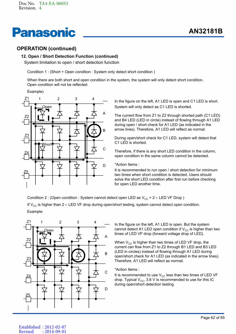
AN32181B
Page 62 of 65
Product Standards
When there are both short and open condition in the system, the system will only detect short condition. Open condition will not be reflected.
Example)
In the figure on the left, A1 LED is open and C1 LED is short.
System will only detect as C1 LED is shorted.
The current flow from Z1 to Z2 through shorted path (C1 LED) and B4 LED (LED in circle) instead of flowing through A1 LED during open / short check for A1 LED (as indicated in the arrow lines). Therefore, A1 LED will reflect as normal.
During open/short check for C1 LED, system will detect that C1 LED is shorted.
Therefore, if there is any short LED condition in the column, open condition in the same column cannot be detected.
*Action Items :
It is recommended to run open / short detection for minimum two times when short condition is detected. Users should solve the short LED condition after first run before checking for open LED another time.
Condition 2 : (Open condition : System cannot detect open LED as VCC > 2 LED VF Drop )
If VCC is higher than 2 LED VF drop during open/short testing, system cannot detect open condition.
Example:
In the figure on the left, A1 LED is open. But the system cannot detect A1 LED open condition if VCC is higher than two times of LED VF drop (forward voltage drop of LED).
When VCC is higher than two times of LED VF drop, the current can flow from Z1 to Z2 through B1 LED and B3 LED (LED in circles) instead of flowing through A1 LED during open/short check for A1 LED (as indicated in the arrow lines). Therefore, A1 LED will reflect as normal.
*Action Items :
It is recommended to use VCC less than two times of LED VF drop. Typical VCC, 3.6 V is recommended to use for this IC during open/short detection testing.
A
B
C
D
1 2 3 4Z1
Z2
Z3
Z4
Z5
Open
1 2 3 4Z1
A
B
C
D
Z2
Z3
Z4
Z5
Open
Short
12. Open / Short Detection Function (continued)
Condition 1 : (Short + Open condition : System only detect short condition )
System limitation to open / short detection function
OPERATION (continued)
Doc No. TA4-EA-06053Revision. 4
Established : 2012-02-07Revised : 2014-09-01
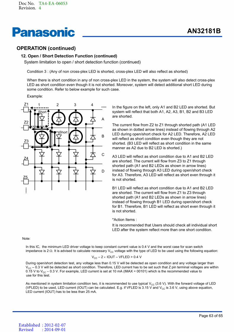
AN32181B
Page 63 of 65
Product Standards
In the figure on the left, only A1 and B2 LED are shorted. But system will reflect that both A1, A2, A3, B1, B2 and B3 LED are shorted.
The current flow from Z2 to Z1 through shorted path (A1 LED as shown in dotted arrow lines) instead of flowing through A2 LED during open/short check for A2 LED. Therefore, A2 LED will reflect as short condition even though they are not shorted. (B3 LED will reflect as short condition in the same manner as A2 due to B2 LED is shorted.)
A3 LED will reflect as short condition due to A1 and B2 LED are shorted. The current will flow from Z3 to Z1 through shorted path (A1 and B2 LEDs as shown in arrow lines) instead of flowing through A3 LED during open/short check for A3. Therefore, A3 LED will reflect as short even through it is not shorted.
B1 LED will reflect as short condition due to A1 and B2 LED are shorted. The current will flow from Z1 to Z3 through shorted path (A1 and B2 LEDs as shown in arrow lines) instead of flowing through B1 LED during open/short check for B1. Therefore, B1 LED will reflect as short even through it is not shorted.
*Action Items :
It is recommended that Users should check all individual short LED after the system reflect more than one short condition.
Note:
In this IC, the minimum LED driver voltage to keep constant current value is 0.4 V and the worst case for scan switch impedance is 2 . It is advised to calculate necessary VCC voltage with the type of LED to be used using the following equation:
VCC – 2 IOUT – VFLED > 0.4 V
During open/short detection test, any voltage less than 0.15 V will be detected as open condition and any voltage larger thanVCC – 0.3 V will be detected as short condition. Therefore, LED current has to be set such that Z pin terminal voltages are within 0.15 V to VCC – 0.3 V. For example, LED current is set at 10 mA (IMAX = 00101) which is the recommended value to use for this test.
As mentioned in system limitation condition two, it is recommended to use typical VCC (3.6 V). With the forward voltage of LED (VFLED) to be used, LED current (IOUT) can be calculated. E.g. if VFLED is 3.15 V and VCC is 3.6 V, using above equation, LED current (IOUT) has to be less than 25 mA.
A
B
C
D
1 2 3 4Z1
Z2
Z3
Z4
Z5
Short
Short
12. Open / Short Detection Function (continued)
Condition 3 : (Any of non cross-plex LED is shorted, cross-plex LED will also reflect as shorted)
When there is short condition in any of non cross-plex LED in the system, the system will also detect cross-plex LED as short condition even though it is not shorted. Moreover, system will detect additional short LED during some condition. Refer to below example for such case.
Example:
System limitation to open / short detection function (continued)
OPERATION (continued)
Doc No. TA4-EA-06053Revision. 4
Established : 2012-02-07Revised : 2014-09-01
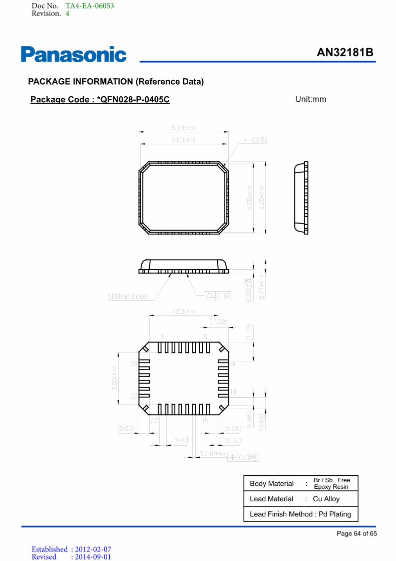
AN32181B
Page 64 of 65
Product Standards
PACKAGE INFORMATION (Reference Data)
Package Code : *QFN028-P-0405C
Lead Finish Method : Pd Plating
Lead Material : Cu Alloy
Body Material : Br / Sb Free Epoxy Resin
Doc No. TA4-EA-06053Revision. 4
Established : 2012-02-07Revised : 2014-09-01

AN32181B
Page 65 of 65
Product Standards
IMPORTANT NOTICE
1. When using the IC for new models, verify the safety including the long-term reliability for each product.
2. When the application system is designed by using this IC, please confirm the notes in this book. Please read the notes to descriptions and the usage notes in the book.
3. This IC is intended to be used for general electronic equipment.Consult our sales staff in advance for information on the following applications: Special applications in which exceptional quality and reliability are required, or if the failure or malfunction of this IC may directly jeopardize life or harm the human body.Any applications other than the standard applications intended.
(1) Space appliance (such as artificial satellite, and rocket)(2) Traffic control equipment (such as for automobile, airplane, train, and ship)(3) Medical equipment for life support(4) Submarine transponder(5) Control equipment for power plant(6) Disaster prevention and security device(7) Weapon(8) Others : Applications of which reliability equivalent to (1) to (7) is required
Our company shall not be held responsible for any damage incurred as a result of or in connection with the IC being used for any special application, unless our company agrees to the use of such special application.
4. This IC is neither designed nor intended for use in automotive applications or environments unless the specific product is designated by our company as compliant with the ISO/TS 16949 requirements.Our company shall not be held responsible for any damage incurred by customers or any third party as a result of or in connection with the IC being used in automotive application, unless our company agrees to such application in this book.
5. Please use this product in compliance with all applicable laws and regulations that regulate the inclusion or use of controlled substances, including without limitation, the EU RoHS Directive. Our company shall not be held responsible for any damage incurred as a result of our IC being used by our customers, not complying with the applicable laws and regulations.
6. Pay attention to the direction of IC. When mounting it in the wrong direction onto the PCB (printed-circuit-board), it might emit smoke or ignite.
7. Pay attention in the PCB (printed-circuit-board) pattern layout in order to prevent damage due to short circuit between pins. In addition, refer to the Pin Description for the pin configuration.
8. Perform visual inspection on the PCB before applying power, otherwise damage might happen due to problems such as solder-bridge between the pins of the semiconductor device. Also, perform full technical verification on the assembly quality, because the same damage possibly can happen due to conductive substances, such as solder ball, that adhere to the IC during transportation.
9. Take notice in the use of this product that it might be damaged or occasionally emit smoke when an abnormal state occurs such as output pin-VCC short (Power supply fault), output pin-GND short (Ground fault), or output-to-output-pin short (load short). Safety measures such as installation of fuses are recommended because the extent of the above-mentioned damage and smoke emission will depend on the current capability of the power supply..
10. The protection circuit is for maintaining safety against abnormal operation. Therefore, the protection circuit should not work during normal operation.Especially for the thermal protection circuit, if the area of safe operation or the absolute maximum rating is momentarily exceeded due to output pin to VCC short (Power supply fault), or output pin to GND short (Ground fault), the IC might be damaged before the thermal protection circuit could operate.
11. Unless specified in the product specifications, make sure that negative voltage or excessive voltage are not applied to thepins because the device might be damaged, which could happen due to negative voltage or excessive voltage generated during the ON and OFF timing when the inductive load of a motor coil or actuator coils of optical pick-up is being driven.
12. Verify the risks which might be caused by the malfunctions of external components.
Doc No. TA4-EA-06053Revision. 4
Established : 2012-02-07Revised : 2014-09-01

Request for your special attention and precautionsin using the technical information and semiconductors described in this book
(1) If any of the products or technical information described in this book is to be exported or provided to non-residents, thelaws and regulations of the exporting country, especially, those with regard to security export control, must be observed.
(2) The technical information described in this book is intended only to show the main characteristics and application circuitexamples of the products. No license is granted in and to any intellectual property right or other right owned byPanasonic Corporation or any other company. Therefore, no responsibility is assumed by our company as to theinfringement upon any such right owned by any other company which may arise as a result of the use of technicalinformation de-scribed in this book.
(3) The products described in this book are intended to be used for general applications (such as office equipment,communications equipment, measuring instruments and household appliances), or for specific applications as expresslystated in this book.Please consult with our sales staff in advance for information on the following applications, moreover please exchangedocuments separately on terms of use etc.: Special applications (such as for in-vehicle equipment, airplanes, aerospace,automotive equipment, traffic signaling equipment, combustion equipment, medical equipment and safety devices) inwhich exceptional quality and reliability are required, or if the failure or malfunction of the products may directlyjeopardize life or harm the human body.Unless exchanging documents on terms of use etc. in advance, it is to be understood that our company shall not be heldresponsible for any damage incurred as a result of or in connection with your using the products described in this bookfor any special application.
(4) The products and product specifications described in this book are subject to change without notice for modificationand/or improvement. At the final stage of your design, purchasing, or use of the products, therefore, ask for the most up-to-date Product Standards in advance to make sure that the latest specifications satisfy your requirements.
(5) When designing your equipment, comply with the range of absolute maximum rating and the guaranteed operatingconditions (operating power supply voltage and operating environment etc.). Especially, please be careful not to exceedthe range of absolute maximum rating on the transient state, such as power-on, power-off and mode-switching. Other-wise, we will not be liable for any defect which may arise later in your equipment.Even when the products are used within the guaranteed values, take into the consideration of incidence of break downand failure mode, possible to occur to semiconductor products. Measures on the systems such as redundant design,arresting the spread of fire or preventing glitch are recommended in order to prevent physical injury, fire, social damages,for example, by using the products.
(6) Comply with the instructions for use in order to prevent breakdown and characteristics change due to external factors(ESD, EOS, thermal stress and mechanical stress) at the time of handling, mounting or at customer's process. We donot guarantee quality for disassembled products or the product re-mounted after removing from the mounting board.When using products for which damp-proof packing is required, satisfy the conditions, such as shelf life and the elapsedtime since first opening the packages.
(7) When reselling products described in this book to other companies without our permission and receiving any claim ofrequest from the resale destination, please understand that customers will bear the burden.
(8) This book may be not reprinted or reproduced whether wholly or partially, without the prior written permission of ourcompany.
No.010618