Embed Size (px)
Citation preview
ZIC2410 - Design Practices When Using Embedded Flash Memory
ZIC24
10 -
Desig
n Pra
ctice
s Whe
n Usin
g Emb
edde
d Flas
h Mem
ory
Application Note
Introduction
CEL’s MeshConnect ZIC2410 is a true single-chip solution, compliant with ZigBee specifications and IEEE802.15.4, a complete wireless solution for all ZigBee applications. The ZIC2410 consists of a Radio Frequency (RF) transceiver with baseband modem, a hardwired Media Access Controller (MAC) and an embedded 8051 microcontroller with integrat-ed Flash memory. The integrated Flash memory can sup-port a number of uses including: program memory, SNAP™ scripts, radio configuration (i.e. channel, PAN ID, security settings), MAC addresses, and data logging. It is convenient and in some cases necessary for certain applications to write to the embedded Flash during device run time.
The process for the programming a Flash memory block includes: loading the Flash page buffer with ‘new data’, erase the target Flash page, then finally write data in Flash buffer to the target Flash page. IMPORTANT: once the erase process is initiated the process must be allowed to continue until completion. Any interruption (i.e. reset, power cycle or unstable power supply) to the ZIC2410 during the Flash erase/program process can corrupt the contents of the Flash memory. Additionally, as the Flash buffer (holding the ‘new’ data) is volatile, it is also affected by power cycle, system reset or an unstable power supply. The system
AN3014: ZIC2410 - Design Practices When Using Embedded Flash Memory
Development Kits Available
ZICM2410P0-KIT2-1Evaluation and Development Kit for both MeshConnect Tranceiver ICs and MeshConnect Module.
ZICM2410P2-KIT1-1Evaluation and Development Kit for both MeshConnect Tranceiver ICs and MeshConnect Module.
affects of corrupted Flash memory are unpredictable and can vary from loss of data, up to an including system program code corruption causing system malfunction, necessitating device reprogramming. To avoid the negative ramifications of corrupted Flash memory is it important for the system designer to follow the design practices outlined in this guide.
This document will outline proper design practices for both hardware and software to mitigate the memory loss during Flash programming. The practices presented in this document are recommended for all designs, however applications which are battery powered, whose power is cycled rapidly or those designs in which the embedded microcontroller writes to the on-chip Flash memory by the nature of the their less stable power supply should pay special attention. The recommended design practices include both software and hardware scenarios, as each application is unique, certain scenarios may not apply to all applications based upon operating environment and conditions and/or component selections.
ZIC2410 - Designing Practices When Using Embedded Flash Memory
ZIC2410 - Design Practices When Using Embedded Flash Memory
Software: Self ProgrammingThe ZIC2410 integrated circuit has the feature, commonly known as Self Programming, of updating or writing to its own internal Flash memory. The ZIC2410 integrated circuit has an operating voltage range from 1.35 Volts to 3.3 Volts. Self Programming must occur and complete above an operating voltage of 1.8 Volts, otherwise successful programming cannot be guaranteed. It is recommended for designs which could operate below 1.8 Volts and utilize the Self-Programming feature that the designer makes use of the devices capability to monitor the supply voltage (ADC Channel 0b0111) prior to initiating the Self Programming operation. The ADC result needs to be greater than 0x4FFF before Self Programming can occur. Failure to adhere to this requirement may result in the writing of incorrect data.
CEL’s MeshConnect Modules based upon the ZIC2410 SoC (ZICM2410P0x and ZICM2410P2x) are not subjected to this software scenario as the operating voltage range is 2.1 Volts to 3.3 Volts, already above the minimum require-ment for Self Programming.
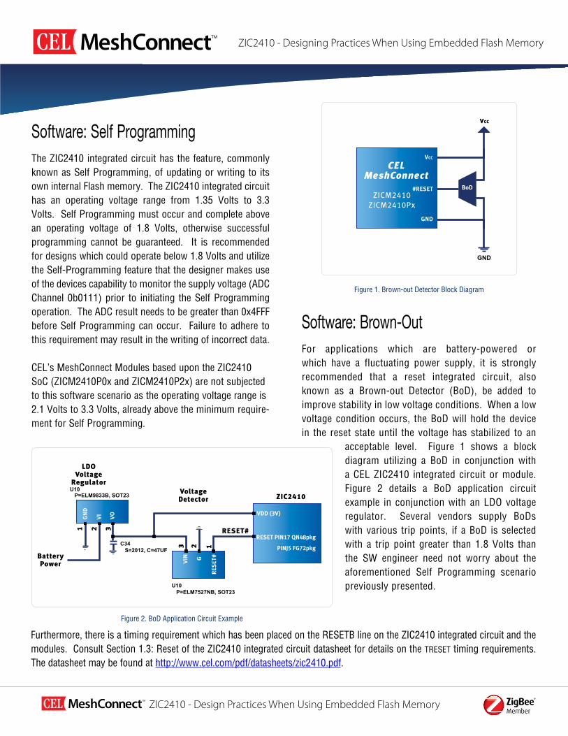
Software: Brown-OutFor applications which are battery-powered or which have a fluctuating power supply, it is strongly recommended that a reset integrated circuit, also known as a Brown-out Detector (BoD), be added to improve stability in low voltage conditions. When a low voltage condition occurs, the BoD will hold the device in the reset state until the voltage has stabilized to an
acceptable level. Figure 1 shows a block diagram utilizing a BoD in conjunction with a CEL ZIC2410 integrated circuit or module. Figure 2 details a BoD application circuit example in conjunction with an LDO voltage regulator. Several vendors supply BoDs with various trip points, if a BoD is selected with a trip point greater than 1.8 Volts than the SW engineer need not worry about the aforementioned Self Programming scenario previously presented.
Figure 2. BoD Application Circuit Example
Figure 1. Brown-out Detector Block Diagram
GND
BoD
VCC
VCC
GND
#RESET
CELMeshConnect
ZICM2410ZICM2410Px
LDOVoltage
RegulatorVoltageDetector ZIC2410
VDD (3V)
RESET PIN17 QN48pkg
PINJ5 FG72pkgBatteryPower
C34 S=2012, C=47UF
U10 P=ELM7527NB, SOT23
U10 P=ELM9833B, SOT23
RESET#1
12
2 3
3V
IN G
RES
ET#
GN
D
VI VO
Furthermore, there is a timing requirement which has been placed on the RESETB line on the ZIC2410 integrated circuit and the modules. Consult Section 1.3: Reset of the ZIC2410 integrated circuit datasheet for details on the TRESET timing requirements. The datasheet may be found at http://www.cel.com/pdf/datasheets/zic2410.pdf.
ZIC2410 - Designing Practices When Using Embedded Flash Memory
ZIC2410 - Design Practices When Using Embedded Flash Memory
Hardware: I/O InterfacingThe ZIC2410 integrated circuit has the capability of supporting split power supplies, one for the microprocessor core and the other for the I/O ring. However, many applications power the microprocessor core and the I/O ring from the same supply and utilize the internal voltage regulator to step-down the microprocessor core voltage. The ZICM2410Px modules utilize the single supply approach as well.
Regardless of supply configuration, the ZIC2410 integrated circuit and ZICM2410Px modules have a requirement that the maximum input voltage, VIH, on any digital pin is no greater than the I/O ring supply voltage. Any digital pin is not solely limited to the general purpose I/Os (GPIO), but also includes the RESETB, MS0, MS1, MS2 and MSV pins. Of primary concern are the later mentioned special function pins. If the application requires interfacing to other voltage levels, a voltage translator is required to properly step the voltages to the operating voltage of the CEL ZIC2410. It is not recommended to have higher voltages on the GPIOs, RESETB, MS0, MS1, MS2 and MSV pins than on I/O ring supply voltage. Doing so can have adverse affects on the Flash memory as some of the special function pins have an influence in the Flash programming process.
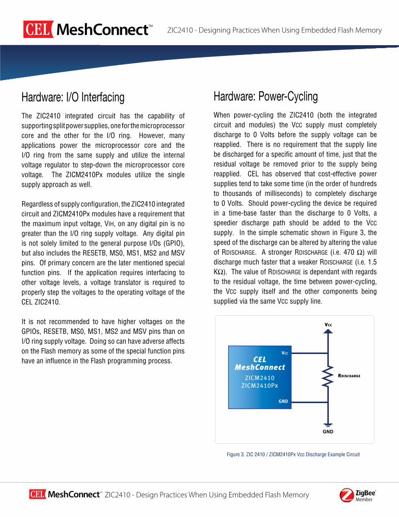
Hardware: Power-CyclingWhen power-cycling the ZIC2410 (both the integrated circuit and modules) the VCC supply must completely discharge to 0 Volts before the supply voltage can be reapplied. There is no requirement that the supply line be discharged for a specific amount of time, just that the residual voltage be removed prior to the supply being reapplied. CEL has observed that cost-effective power supplies tend to take some time (in the order of hundreds to thousands of milliseconds) to completely discharge to 0 Volts. Should power-cycling the device be required in a time-base faster than the discharge to 0 Volts, a speedier discharge path should be added to the VCC supply. In the simple schematic shown in Figure 3, the speed of the discharge can be altered by altering the value of RDISCHARGE. A stronger RDISCHARGE (i.e. 470 Ω) will discharge much faster that a weaker RDISCHARGE (i.e. 1.5 KΩ). The value of RDISCHARGE is dependant with regards to the residual voltage, the time between power-cycling, the VCC supply itself and the other components being supplied via the same VCC supply line.
Figure 3. ZIC 2410 / ZICM2410Px Vcc Discharge Example Circuit
GND
VCC
VCC
RDISCHARGE
GND
CELMeshConnect
ZICM2410ZICM2410Px

ZIC2410 - Designing Practices When Using Embedded Flash Memory
California Eastern Laboratories 4590 Patrick Henry DriveSanta Clara, CA 95054(408) 919-2500
Professional Grade Wireless Radio Solutions
www.cel.com
ConclusionThe procedures outlined in this document have proven to mitigate the unintentional corruption of the on-chip Flash memory with regards to ZIC2410 integrated circuit or the ZIC2410-based modules. Customers who experienced the unintentional erasures and implemented the recommended design practices have reported no erasures since implementation of the aforementioned recommendations.
Related Documents
MeshConnect Module Data Sheet
MeshConnect Extended Range Data Sheet
ZIC2410 Data Sheet
SNAP Software - Quick Start Guide
MeshConnect LED Daughter Card Demo
About CEL California Eastern Laboratories (CEL) has over 50 years of experience providing a wide range of RF and wireless semiconductors, Optocou-plers and Solid State Relays, Fiber Optics and Detectors. CEL devel-ops the MeshConnect™ line of professional grade modules that pro-vide hardware and software solutions in the 2.4 GHZ (IEEE 802.15.4/SNAP/ZigBee) and Sub-Ghz (868/915 MHz) frequency ranges. These solutions offer customers qualified and certified platforms that greatly simplify design and greatly reduce time to market. For more information, visit our MeshConnect products and solutions at www.cel.com/MeshConnect.
05.24.2011