Embed Size (px)
Citation preview
ISL6752/54EVAL1Z ZVS DC/DC Power Supply with Synchronous Rectifiers Evaluation Board
USER’S MANUAL
AN1603Rev.2.00
May 25, 2018
AbstractThe ISL6752/54EVAL1Z is a new design based on the ISL6752EVAL1Z but with several design modifications to improve the efficiency from 90% to 95%. The control circuit has been moved off the main board onto a daughter card. Two different daughter cards are provided: one using the ISL6752 and the other using the ISL6754. Both control cards use the Intersil Zero Voltage Switching (ZVS) topology. The ISL6752 daughter card features pulse by pulse current limiting, and the ISL6754 daughter card features a patented method for average current limiting that results in a brick-wall current limit profile.
The ISL6752/54EVAL1Z Printed Circuit Board (PCB) layout has also been greatly improved over the ISL6752EVAL1Z. Even though the overall size of the board has been reduced, the copper losses have been reduced as well.
In addition to the ZVS function, this board also incorporates N-Channel FETs as secondary side rectifiers, also known as Synchronous Rectifiers (SR). Power dissipation of the secondary side rectifiers is reduced because the conduction losses of SRs are significantly less than the conduction losses of PN or Schottky diodes.
Table of ContentsScope . . . . . . . . . . . . . . . . . . . . . . . . . . . . . . . . . . . . . . . . . . . . . . . . . . . . . . . . . . . . . . . . . . . . . . . . . . . . . . . . . . . . . . . . . . . . . . . . . . . . . . 3
Block Diagram . . . . . . . . . . . . . . . . . . . . . . . . . . . . . . . . . . . . . . . . . . . . . . . . . . . . . . . . . . . . . . . . . . . . . . . . . . . . . . . . . . . . . . . . . . . . . . 4Daughter Cards . . . . . . . . . . . . . . . . . . . . . . . . . . . . . . . . . . . . . . . . . . . . . . . . . . . . . . . . . . . . . . . . . . . . . . . . . . . . . . . . . . . . . . . . . . . . . . . . . . .4ZVS Full Bridge . . . . . . . . . . . . . . . . . . . . . . . . . . . . . . . . . . . . . . . . . . . . . . . . . . . . . . . . . . . . . . . . . . . . . . . . . . . . . . . . . . . . . . . . . . . . . . . . . . . .5High Voltage Protection . . . . . . . . . . . . . . . . . . . . . . . . . . . . . . . . . . . . . . . . . . . . . . . . . . . . . . . . . . . . . . . . . . . . . . . . . . . . . . . . . . . . . . . . . . . .5Primary Side Current Sensing . . . . . . . . . . . . . . . . . . . . . . . . . . . . . . . . . . . . . . . . . . . . . . . . . . . . . . . . . . . . . . . . . . . . . . . . . . . . . . . . . . . . . . .6Synchronous Rectifier Drive Circuit . . . . . . . . . . . . . . . . . . . . . . . . . . . . . . . . . . . . . . . . . . . . . . . . . . . . . . . . . . . . . . . . . . . . . . . . . . . . . . . . . . .6Current Doubler Output. . . . . . . . . . . . . . . . . . . . . . . . . . . . . . . . . . . . . . . . . . . . . . . . . . . . . . . . . . . . . . . . . . . . . . . . . . . . . . . . . . . . . . . . . . . . .6
Basic SR Principles . . . . . . . . . . . . . . . . . . . . . . . . . . . . . . . . . . . . . . . . . . . . . . . . . . . . . . . . . . . . . . . . . . . . . . . . . . . . . . . . . . . . . . . . . . 7SR Drive Timing Requirements . . . . . . . . . . . . . . . . . . . . . . . . . . . . . . . . . . . . . . . . . . . . . . . . . . . . . . . . . . . . . . . . . . . . . . . . . . . . . . . . . . . . . .7SR Drive and Bias . . . . . . . . . . . . . . . . . . . . . . . . . . . . . . . . . . . . . . . . . . . . . . . . . . . . . . . . . . . . . . . . . . . . . . . . . . . . . . . . . . . . . . . . . . . . . . . . .8Current Doubler . . . . . . . . . . . . . . . . . . . . . . . . . . . . . . . . . . . . . . . . . . . . . . . . . . . . . . . . . . . . . . . . . . . . . . . . . . . . . . . . . . . . . . . . . . . . . . . . . . .8
Current Sensing . . . . . . . . . . . . . . . . . . . . . . . . . . . . . . . . . . . . . . . . . . . . . . . . . . . . . . . . . . . . . . . . . . . . . . . . . . . . . . . . . . . . . . . . . . . . 10
Conclusion . . . . . . . . . . . . . . . . . . . . . . . . . . . . . . . . . . . . . . . . . . . . . . . . . . . . . . . . . . . . . . . . . . . . . . . . . . . . . . . . . . . . . . . . . . . . . . . . 11
References . . . . . . . . . . . . . . . . . . . . . . . . . . . . . . . . . . . . . . . . . . . . . . . . . . . . . . . . . . . . . . . . . . . . . . . . . . . . . . . . . . . . . . . . . . . . . . . . 12
Evaluation Board Set-up . . . . . . . . . . . . . . . . . . . . . . . . . . . . . . . . . . . . . . . . . . . . . . . . . . . . . . . . . . . . . . . . . . . . . . . . . . . . . . . . . . . . . 12
Setting Up . . . . . . . . . . . . . . . . . . . . . . . . . . . . . . . . . . . . . . . . . . . . . . . . . . . . . . . . . . . . . . . . . . . . . . . . . . . . . . . . . . . . . . . . . . . . . . . . . 12Danger. . . . . . . . . . . . . . . . . . . . . . . . . . . . . . . . . . . . . . . . . . . . . . . . . . . . . . . . . . . . . . . . . . . . . . . . . . . . . . . . . . . . . . . . . . . . . . . . . . . . . . . . . 12Caution . . . . . . . . . . . . . . . . . . . . . . . . . . . . . . . . . . . . . . . . . . . . . . . . . . . . . . . . . . . . . . . . . . . . . . . . . . . . . . . . . . . . . . . . . . . . . . . . . . . . . . . . 12
Waveforms . . . . . . . . . . . . . . . . . . . . . . . . . . . . . . . . . . . . . . . . . . . . . . . . . . . . . . . . . . . . . . . . . . . . . . . . . . . . . . . . . . . . . . . . . . . . . . . . 13ZVS. . . . . . . . . . . . . . . . . . . . . . . . . . . . . . . . . . . . . . . . . . . . . . . . . . . . . . . . . . . . . . . . . . . . . . . . . . . . . . . . . . . . . . . . . . . . . . . . . . . . . . . . . . . . 13ZVS Waveforms . . . . . . . . . . . . . . . . . . . . . . . . . . . . . . . . . . . . . . . . . . . . . . . . . . . . . . . . . . . . . . . . . . . . . . . . . . . . . . . . . . . . . . . . . . . . . . . . . 13Load Transients Waveforms. . . . . . . . . . . . . . . . . . . . . . . . . . . . . . . . . . . . . . . . . . . . . . . . . . . . . . . . . . . . . . . . . . . . . . . . . . . . . . . . . . . . . . . 14Output Ripple and Noise Waveforms . . . . . . . . . . . . . . . . . . . . . . . . . . . . . . . . . . . . . . . . . . . . . . . . . . . . . . . . . . . . . . . . . . . . . . . . . . . . . . . 17Transformer Current, Primary Winding Waveforms . . . . . . . . . . . . . . . . . . . . . . . . . . . . . . . . . . . . . . . . . . . . . . . . . . . . . . . . . . . . . . . . . . . 18
Performance Curves . . . . . . . . . . . . . . . . . . . . . . . . . . . . . . . . . . . . . . . . . . . . . . . . . . . . . . . . . . . . . . . . . . . . . . . . . . . . . . . . . . . . . . . . 19
PCB Layout . . . . . . . . . . . . . . . . . . . . . . . . . . . . . . . . . . . . . . . . . . . . . . . . . . . . . . . . . . . . . . . . . . . . . . . . . . . . . . . . . . . . . . . . . . . . . . . . 20
Schematics- Main Board, ISL6752/54EVAL1Z . . . . . . . . . . . . . . . . . . . . . . . . . . . . . . . . . . . . . . . . . . . . . . . . . . . . . . . . . . . . . . . . . . 25
Schematics - Daughter Card . . . . . . . . . . . . . . . . . . . . . . . . . . . . . . . . . . . . . . . . . . . . . . . . . . . . . . . . . . . . . . . . . . . . . . . . . . . . . . . . . 27
Bill of Materials . . . . . . . . . . . . . . . . . . . . . . . . . . . . . . . . . . . . . . . . . . . . . . . . . . . . . . . . . . . . . . . . . . . . . . . . . . . . . . . . . . . . . . . . . . . . 28
AN1603 Rev.2.00 Page 1 of 33May 25, 2018
ISL6752/54EVAL1Z ZVS DC/DC Power Supply with
Synchronous Rectifiers Evaluation Board
List of FiguresFIGURE 1. NEW ISL6752/54EVAL1Z . . . . . . . . . . . . . . . . . . . . . . . . . . . . . . . . . . . . . . . . . . . . . . . . . . . . . . . . . . . . . . . . . . . . . . . . . . . . . . . . . .3FIGURE 2. ISL6752/54EVAL1Z BLOCK DIAGRAM. . . . . . . . . . . . . . . . . . . . . . . . . . . . . . . . . . . . . . . . . . . . . . . . . . . . . . . . . . . . . . . . . . . . . . . .4FIGURE 3. ISL6752 DAUGHTER CARD. . . . . . . . . . . . . . . . . . . . . . . . . . . . . . . . . . . . . . . . . . . . . . . . . . . . . . . . . . . . . . . . . . . . . . . . . . . . . . . . . .4FIGURE 4. ISL6754 DAUGHTER CARD . . . . . . . . . . . . . . . . . . . . . . . . . . . . . . . . . . . . . . . . . . . . . . . . . . . . . . . . . . . . . . . . . . . . . . . . . . . . . . . . .5FIGURE 5. FULL BRIDGE . . . . . . . . . . . . . . . . . . . . . . . . . . . . . . . . . . . . . . . . . . . . . . . . . . . . . . . . . . . . . . . . . . . . . . . . . . . . . . . . . . . . . . . . . . . . .5FIGURE 6. PROTECTION CIRCUITS . . . . . . . . . . . . . . . . . . . . . . . . . . . . . . . . . . . . . . . . . . . . . . . . . . . . . . . . . . . . . . . . . . . . . . . . . . . . . . . . . . . . .5FIGURE 7. PRIMARY SIDE CURRENT SENSING . . . . . . . . . . . . . . . . . . . . . . . . . . . . . . . . . . . . . . . . . . . . . . . . . . . . . . . . . . . . . . . . . . . . . . . . . .6FIGURE 8. SRs AND DRIVERS. . . . . . . . . . . . . . . . . . . . . . . . . . . . . . . . . . . . . . . . . . . . . . . . . . . . . . . . . . . . . . . . . . . . . . . . . . . . . . . . . . . . . . . . .6FIGURE 9. PULSE TRANSFORMER AND DRIVER . . . . . . . . . . . . . . . . . . . . . . . . . . . . . . . . . . . . . . . . . . . . . . . . . . . . . . . . . . . . . . . . . . . . . . . . .6FIGURE 10. CURRENT DOUBLER OUTPUT . . . . . . . . . . . . . . . . . . . . . . . . . . . . . . . . . . . . . . . . . . . . . . . . . . . . . . . . . . . . . . . . . . . . . . . . . . . . . . . .7FIGURE 11. TIMING FOR SRs AND BRIDGE FETs . . . . . . . . . . . . . . . . . . . . . . . . . . . . . . . . . . . . . . . . . . . . . . . . . . . . . . . . . . . . . . . . . . . . . . . . . .7FIGURE 12. SIMPLIFIED SR DRIVE SCHEMATIC . . . . . . . . . . . . . . . . . . . . . . . . . . . . . . . . . . . . . . . . . . . . . . . . . . . . . . . . . . . . . . . . . . . . . . . . . . .8FIGURE 13. CURRENT FLOW IN TWO INDUCTORS OF CURRENT DOUBLER TOPOLOGY . . . . . . . . . . . . . . . . . . . . . . . . . . . . . . . . . . . . . . . . . .9FIGURE 14. INDUCTOR CURRENT WAVEFORMS. . . . . . . . . . . . . . . . . . . . . . . . . . . . . . . . . . . . . . . . . . . . . . . . . . . . . . . . . . . . . . . . . . . . . . . . . . .9FIGURE 15. PRIMARY SIDE CURRENT SENSING CIRCUIT USING ONE CT . . . . . . . . . . . . . . . . . . . . . . . . . . . . . . . . . . . . . . . . . . . . . . . . . . . . 10FIGURE 16. PERFORMANCE OF CURRENT SENSING OUTPUT . . . . . . . . . . . . . . . . . . . . . . . . . . . . . . . . . . . . . . . . . . . . . . . . . . . . . . . . . . . . . 10FIGURE 17. NO LOAD SENSE VOLTAGE ACROSS RS . . . . . . . . . . . . . . . . . . . . . . . . . . . . . . . . . . . . . . . . . . . . . . . . . . . . . . . . . . . . . . . . . . . . . 10FIGURE 18. PLACEMENT OF TWO CURRENT SENSING TRANSFORMERS . . . . . . . . . . . . . . . . . . . . . . . . . . . . . . . . . . . . . . . . . . . . . . . . . . . . 11FIGURE 19. CURRENT SENSING TRANSFORMER IN THE COMMON SOURCE LEAD. . . . . . . . . . . . . . . . . . . . . . . . . . . . . . . . . . . . . . . . . . . . 11FIGURE 20. CURRENT SENSING TRANSFORMER IN THE COMMON DRAIN LEAD . . . . . . . . . . . . . . . . . . . . . . . . . . . . . . . . . . . . . . . . . . . . . 11FIGURE 21. RESONANT SWITCHING WITH 100% (50A) LOAD . . . . . . . . . . . . . . . . . . . . . . . . . . . . . . . . . . . . . . . . . . . . . . . . . . . . . . . . . . . . . 13FIGURE 22. RESONANT SWITCHING WITH 50% (25A) LOAD . . . . . . . . . . . . . . . . . . . . . . . . . . . . . . . . . . . . . . . . . . . . . . . . . . . . . . . . . . . . . . 13FIGURE 23. STEP LOAD: 0A TO 12.5A (12.5A DELTA) . . . . . . . . . . . . . . . . . . . . . . . . . . . . . . . . . . . . . . . . . . . . . . . . . . . . . . . . . . . . . . . . . . . . 14FIGURE 24. STEP LOAD: 25A TO 37.5A (12.5A DELTA) . . . . . . . . . . . . . . . . . . . . . . . . . . . . . . . . . . . . . . . . . . . . . . . . . . . . . . . . . . . . . . . . . . . 14FIGURE 25. STEP LOAD: 37.5A TO 50A . . . . . . . . . . . . . . . . . . . . . . . . . . . . . . . . . . . . . . . . . . . . . . . . . . . . . . . . . . . . . . . . . . . . . . . . . . . . . . . . 15FIGURE 26. STEP LOAD: 0A TO 25A. . . . . . . . . . . . . . . . . . . . . . . . . . . . . . . . . . . . . . . . . . . . . . . . . . . . . . . . . . . . . . . . . . . . . . . . . . . . . . . . . . . 15FIGURE 27. STEP LOAD: 0A TO 50A. . . . . . . . . . . . . . . . . . . . . . . . . . . . . . . . . . . . . . . . . . . . . . . . . . . . . . . . . . . . . . . . . . . . . . . . . . . . . . . . . . . 16FIGURE 28. SHORT CIRCUIT RELEASE WITH ISL6754. . . . . . . . . . . . . . . . . . . . . . . . . . . . . . . . . . . . . . . . . . . . . . . . . . . . . . . . . . . . . . . . . . . . 16FIGURE 29. OUTPUT RIPPLE, 50A LOAD, 40MHz BANDWIDTH . . . . . . . . . . . . . . . . . . . . . . . . . . . . . . . . . . . . . . . . . . . . . . . . . . . . . . . . . . . . .17FIGURE 30. OUTPUT RIPPLE, 50A LOAD, 145MHz BANDWIDTH . . . . . . . . . . . . . . . . . . . . . . . . . . . . . . . . . . . . . . . . . . . . . . . . . . . . . . . . . . . .17FIGURE 31. PRIMARY TRANSFORMER CURRENT vs OUTPUT LOAD TRANSIENT (25A TO 50A). . . . . . . . . . . . . . . . . . . . . . . . . . . . . . . . . . 18FIGURE 32. PRIMARY TRANSFORMER CURRENT vs OUTPUT LOAD TRANSIENT (50A TO 25A). . . . . . . . . . . . . . . . . . . . . . . . . . . . . . . . . . 18FIGURE 33. POWER EFFICIENCY vs LOAD (ISL6752 OR ISL6754) . . . . . . . . . . . . . . . . . . . . . . . . . . . . . . . . . . . . . . . . . . . . . . . . . . . . . . . . . 19FIGURE 34. LOAD REGULATION . . . . . . . . . . . . . . . . . . . . . . . . . . . . . . . . . . . . . . . . . . . . . . . . . . . . . . . . . . . . . . . . . . . . . . . . . . . . . . . . . . . . . . 19FIGURE 35. PULSE BY PULSE vs AVERAGE CURRENT LIMIT . . . . . . . . . . . . . . . . . . . . . . . . . . . . . . . . . . . . . . . . . . . . . . . . . . . . . . . . . . . . . . . 19FIGURE 36. SILKSCREEN TOP. . . . . . . . . . . . . . . . . . . . . . . . . . . . . . . . . . . . . . . . . . . . . . . . . . . . . . . . . . . . . . . . . . . . . . . . . . . . . . . . . . . . . . . . 20FIGURE 37. LAYER 1 . . . . . . . . . . . . . . . . . . . . . . . . . . . . . . . . . . . . . . . . . . . . . . . . . . . . . . . . . . . . . . . . . . . . . . . . . . . . . . . . . . . . . . . . . . . . . . . 21FIGURE 38. LAYER 2 . . . . . . . . . . . . . . . . . . . . . . . . . . . . . . . . . . . . . . . . . . . . . . . . . . . . . . . . . . . . . . . . . . . . . . . . . . . . . . . . . . . . . . . . . . . . . . . 22FIGURE 39. LAYER 3 . . . . . . . . . . . . . . . . . . . . . . . . . . . . . . . . . . . . . . . . . . . . . . . . . . . . . . . . . . . . . . . . . . . . . . . . . . . . . . . . . . . . . . . . . . . . . . . 23FIGURE 40. LAYER 4 . . . . . . . . . . . . . . . . . . . . . . . . . . . . . . . . . . . . . . . . . . . . . . . . . . . . . . . . . . . . . . . . . . . . . . . . . . . . . . . . . . . . . . . . . . . . . . . 24FIGURE 41. MAIN BOARD, PRIMARY, ISL6752_54EVAL1Z . . . . . . . . . . . . . . . . . . . . . . . . . . . . . . . . . . . . . . . . . . . . . . . . . . . . . . . . . . . . . . . 25FIGURE 42. MAIN BOARD, SECONDARY, ISL6752_54EVAL1Z. . . . . . . . . . . . . . . . . . . . . . . . . . . . . . . . . . . . . . . . . . . . . . . . . . . . . . . . . . . . . 26FIGURE 43. DAUGHTER CARD, ISL6754DBEVAL . . . . . . . . . . . . . . . . . . . . . . . . . . . . . . . . . . . . . . . . . . . . . . . . . . . . . . . . . . . . . . . . . . . . . . . . 27FIGURE 44. DAUGHTER CARD, ISL6752DBEVAL1Z . . . . . . . . . . . . . . . . . . . . . . . . . . . . . . . . . . . . . . . . . . . . . . . . . . . . . . . . . . . . . . . . . . . . . . 28
AN1603 Rev.2.00 Page 2 of 33May 25, 2018
ISL6752/54EVAL1Z ZVS DC/DC Power Supply with
Synchronous Rectifiers Evaluation Board
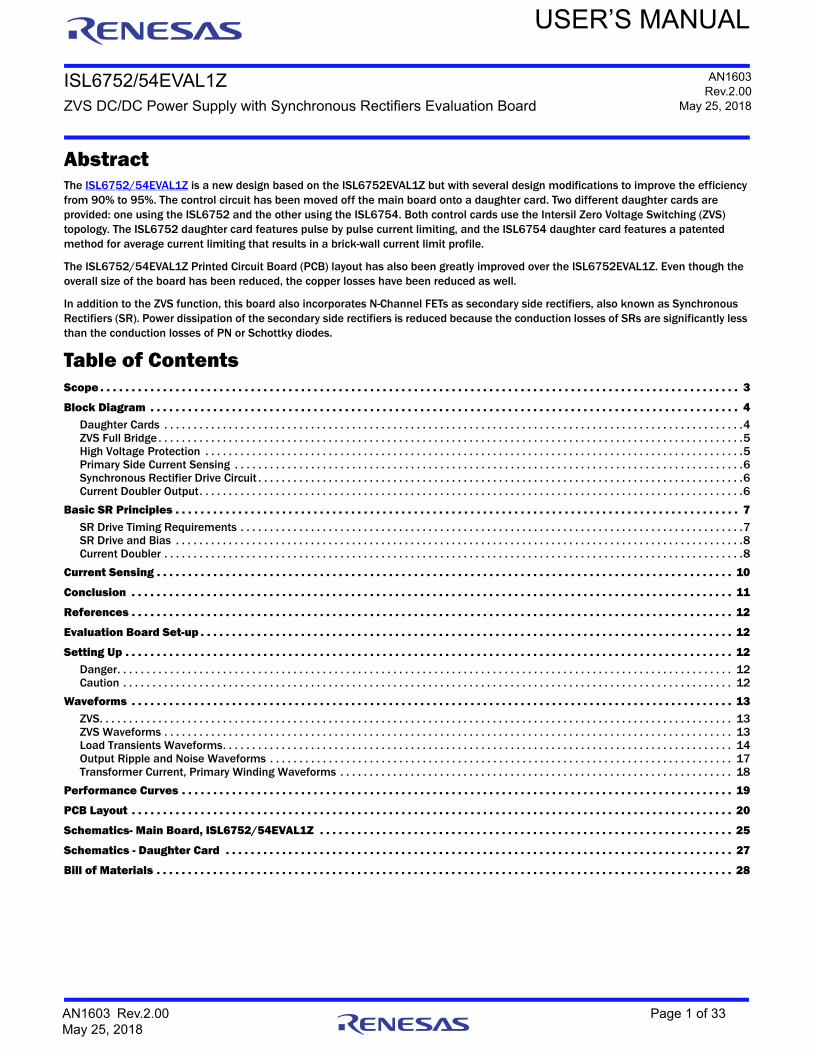
ScopeThis application note covers implementation of Synchronous Rectifiers (SRs) and their associated drive circuits as used on the ISL6752/54EVAL1Z board. Implementation of the primary side ZVS controller, based on the ISL6752 daughter card, is described extensively in Intersil Application Note AN1262, “Designing with the ISL6752, ISL6753 ZVS Full-Bridge Controllers.”
Also reviewed is the performance of this evaluation board. Oscillographs illustrate the performance of the power supply with load transients on the output. The ZVS switching of the bridge FETs is shown, and efficiency and load regulation are measured.
At the end of this application note, the schematics, Bill of Materials (BOM), and PCB layouts are included for reference.
TABLE 1. SPECIFICATIONS
Absolute Maximum Input Voltage 450VDC
Operating Input Voltage 350VDC to 450VDC
Maximum Input Current 2.5ADC
Rated Output Current 50ADC
Current Limit 60A ± 5%
Output Voltage 12V ± 5%
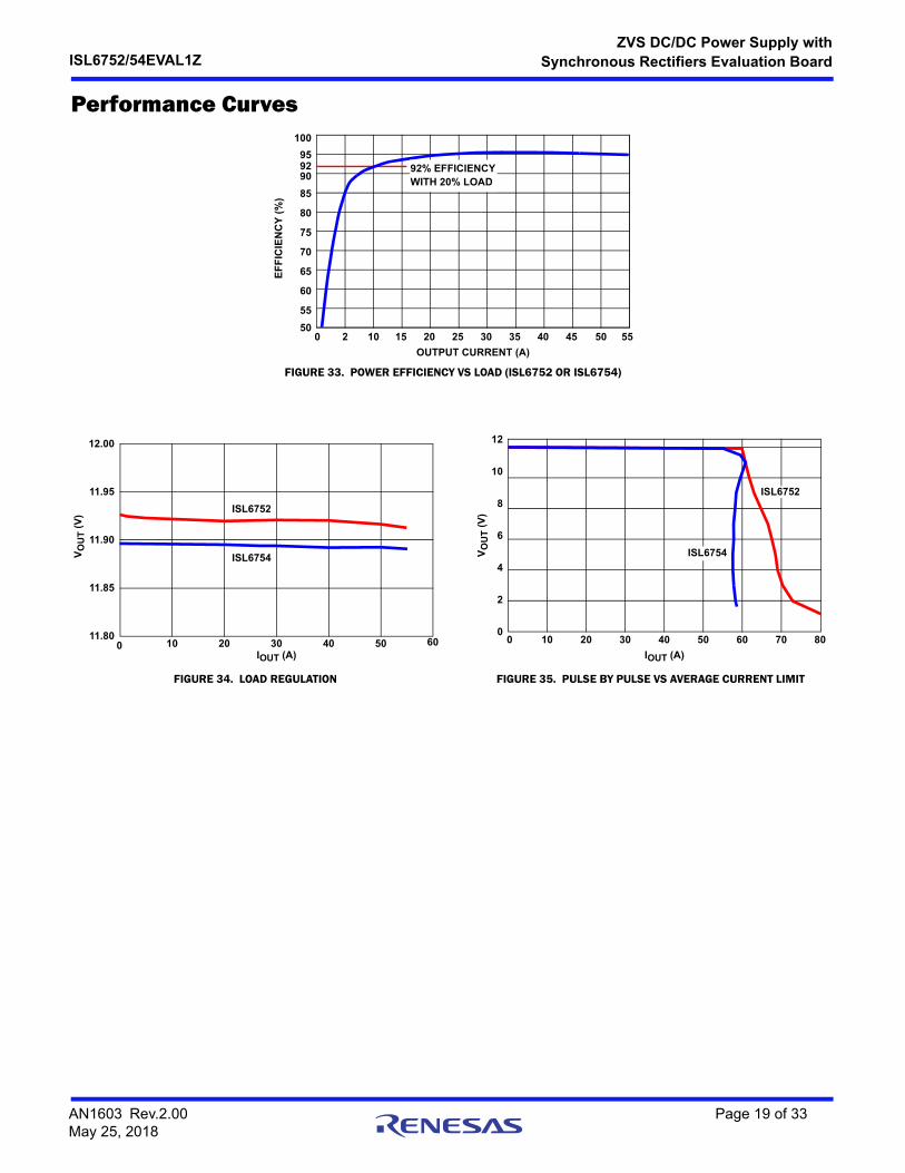
Efficiency at 100% (50A) Load 95%
Efficiency at 20% (10A) Load 92%
FIGURE 1. NEW ISL6752/54EVAL1Z
AN1603 Rev.2.00 Page 3 of 33May 25, 2018
ISL6752/54EVAL1Z ZVS DC/DC Power Supply with
Synchronous Rectifiers Evaluation Board
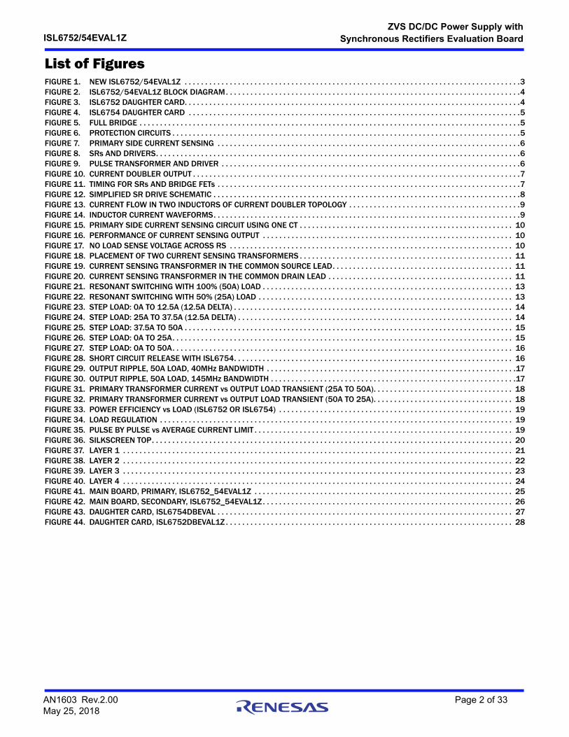
Block DiagramThe evaluation board is composed of several distinct circuit elements. The three main sections are the ZVS full bridge on the input, the current doubler rectifier on the output, and the controller daughter card. See “Schematics- Main Board, ISL6752/54EVAL1Z” on page 25 and “Schematics - Daughter Card” on page 27 for complete circuit details.
Daughter CardsThe ISL6752 and ISL6754 control ICs are located on their respective daughter cards, as shown in Figures 3 and 4. Both daughter cards have the control ICs on the primary side and the voltage error amplifier on the secondary side. Creepage spacing between the primary and secondary is maintained on the cards.
The ISL6752 and the ISL6754 control ICs are located on the primary side, eliminating the need for two AC line isolating gate drive transformers to drive the primary side bridge FETs. Instead, the low side FETs are driven directly by MOSFET drivers (on the main board), and the high side FETs are driven by a gate drive transformer that only requires operational insulation. Primary side control also simplifies design of the current sensing transformers because they also do not have to be AC line isolating.
A line isolation rated opto-coupler (D5 on the ISL6752DB or D2 on the ISL6754DB) passes the analog error signal generated by the error amplifier, U1, from the secondary to the primary. Opto D3 passes a digital signal from primary to secondary to turn off the SRS for diode emulation.
The only functional difference between the ISL6752 and ISL6754 daughter cards is how current limit is implemented. The ISL6752 uses pulse-by-pulse current limit, and the ISL6754 uses average current limit.
400V
ZVS FULL BRIDGE
DAUGHTER CARD
CURRENT DOUBLER RECTIFIER
VOLTAGE CLAMP12.6V
12VDC
VOLTAGE ERROR AMP
BRIDGE CURRENT
SENSE
OPTO-ISOLATOR
ISL6752 OR
ISL6754 CONTROLLER
POWER TRANSFORMER
BRIDGE DRIVES
BIAS
SR DRIVES
PULSE TRANSFORMER
BRIDGE FETsSYNCHRONOUS
RECTIFIERSOUTPUT FILTER
BIAS
SR DRIVERS WITH DELAYSBRIDGE
DRIVERS
PRIMARY
SECONDARY
FIGURE 2. ISL6752/54EVAL1Z BLOCK DIAGRAM
FIGURE 3. ISL6752 DAUGHTER CARD
AN1603 Rev.2.00 Page 4 of 33May 25, 2018
ISL6752/54EVAL1Z ZVS DC/DC Power Supply with
Synchronous Rectifiers Evaluation Board
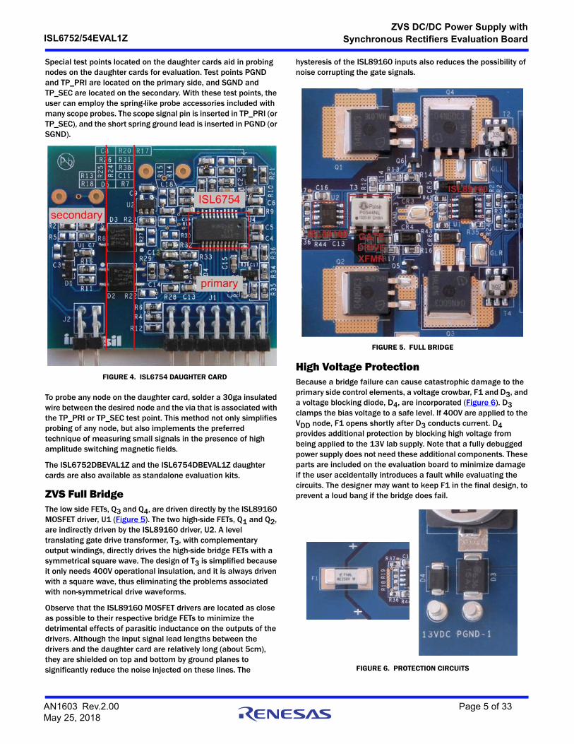
Special test points located on the daughter cards aid in probing nodes on the daughter cards for evaluation. Test points PGND and TP_PRI are located on the primary side, and SGND and TP_SEC are located on the secondary. With these test points, the user can employ the spring-like probe accessories included with many scope probes. The scope signal pin is inserted in TP_PRI (or TP_SEC), and the short spring ground lead is inserted in PGND (or SGND).
To probe any node on the daughter card, solder a 30ga insulated wire between the desired node and the via that is associated with the TP_PRI or TP_SEC test point. This method not only simplifies probing of any node, but also implements the preferred technique of measuring small signals in the presence of high amplitude switching magnetic fields.
The ISL6752DBEVAL1Z and the ISL6754DBEVAL1Z daughter cards are also available as standalone evaluation kits.
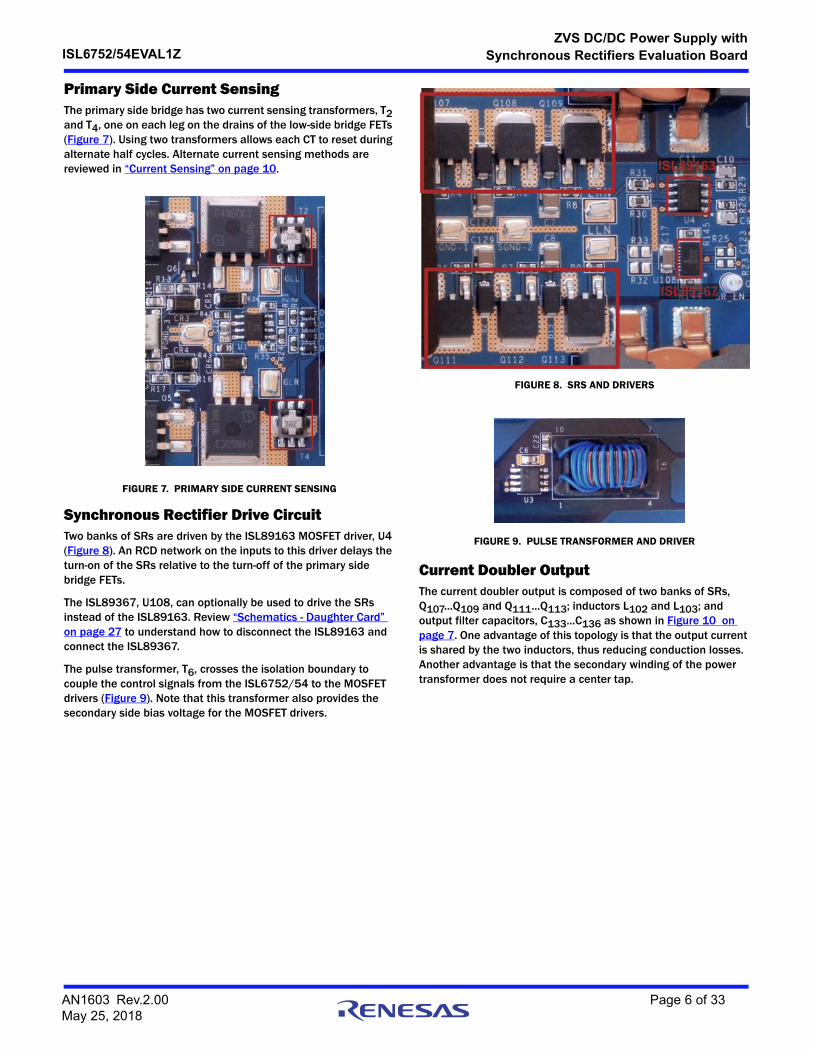
ZVS Full BridgeThe low side FETs, Q3 and Q4, are driven directly by the ISL89160 MOSFET driver, U1 (Figure 5). The two high-side FETs, Q1 and Q2, are indirectly driven by the ISL89160 driver, U2. A level translating gate drive transformer, T3, with complementary output windings, directly drives the high-side bridge FETs with a symmetrical square wave. The design of T3 is simplified because it only needs 400V operational insulation, and it is always driven with a square wave, thus eliminating the problems associated with non-symmetrical drive waveforms.
Observe that the ISL89160 MOSFET drivers are located as close as possible to their respective bridge FETs to minimize the detrimental effects of parasitic inductance on the outputs of the drivers. Although the input signal lead lengths between the drivers and the daughter card are relatively long (about 5cm), they are shielded on top and bottom by ground planes to significantly reduce the noise injected on these lines. The
hysteresis of the ISL89160 inputs also reduces the possibility of noise corrupting the gate signals.
High Voltage ProtectionBecause a bridge failure can cause catastrophic damage to the primary side control elements, a voltage crowbar, F1 and D3, and a voltage blocking diode, D4, are incorporated (Figure 6). D3 clamps the bias voltage to a safe level. If 400V are applied to the VDD node, F1 opens shortly after D3 conducts current. D4 provides additional protection by blocking high voltage from being applied to the 13V lab supply. Note that a fully debugged power supply does not need these additional components. These parts are included on the evaluation board to minimize damage if the user accidentally introduces a fault while evaluating the circuits. The designer may want to keep F1 in the final design, to prevent a loud bang if the bridge does fail.
FIGURE 4. ISL6754 DAUGHTER CARD
FIGURE 5. FULL BRIDGE
FIGURE 6. PROTECTION CIRCUITS
AN1603 Rev.2.00 Page 5 of 33May 25, 2018
ISL6752/54EVAL1Z ZVS DC/DC Power Supply with
Synchronous Rectifiers Evaluation Board
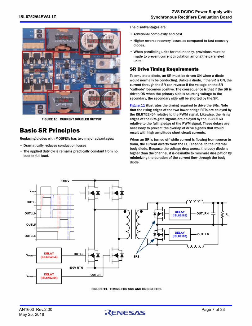
Primary Side Current SensingThe primary side bridge has two current sensing transformers, T2 and T4, one on each leg on the drains of the low-side bridge FETs (Figure 7). Using two transformers allows each CT to reset during alternate half cycles. Alternate current sensing methods are reviewed in “Current Sensing” on page 10.
Synchronous Rectifier Drive CircuitTwo banks of SRs are driven by the ISL89163 MOSFET driver, U4 (Figure 8). An RCD network on the inputs to this driver delays the turn-on of the SRs relative to the turn-off of the primary side bridge FETs.
The ISL89367, U108, can optionally be used to drive the SRs instead of the ISL89163. Review “Schematics - Daughter Card” on page 27 to understand how to disconnect the ISL89163 and connect the ISL89367.
The pulse transformer, T6, crosses the isolation boundary to couple the control signals from the ISL6752/54 to the MOSFET drivers (Figure 9). Note that this transformer also provides the secondary side bias voltage for the MOSFET drivers.
Current Doubler OutputThe current doubler output is composed of two banks of SRs, Q107...Q109 and Q111...Q113; inductors L102 and L103; and output filter capacitors, C133...C136 as shown in Figure 10 on page 7. One advantage of this topology is that the output current is shared by the two inductors, thus reducing conduction losses. Another advantage is that the secondary winding of the power transformer does not require a center tap.
FIGURE 7. PRIMARY SIDE CURRENT SENSING
FIGURE 8. SRS AND DRIVERS
FIGURE 9. PULSE TRANSFORMER AND DRIVER
AN1603 Rev.2.00 Page 6 of 33May 25, 2018
ISL6752/54EVAL1Z ZVS DC/DC Power Supply with
Synchronous Rectifiers Evaluation Board
Basic SR PrinciplesReplacing diodes with MOSFETs has two major advantages:
• Dramatically reduces conduction losses
• The applied duty cycle remains practically constant from no load to full load.
The disadvantages are:
• Additional complexity and cost
• Higher reverse recovery losses as compared to fast recovery diodes.
• When paralleling units for redundancy, provisions must be made to prevent current circulation among the paralleled units.
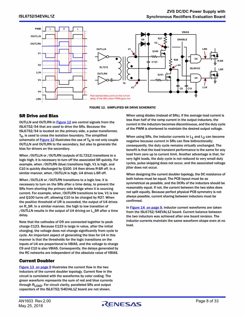
SR Drive Timing RequirementsTo emulate a diode, an SR must be driven ON when a diode would normally be conducting. Unlike a diode, if the SR is ON, the current through the SR can reverse if the voltage on the SR “cathode” becomes positive. The consequence is that if the SR is driven ON when the primary side is sourcing voltage to the secondary, the secondary side will be shorted by the SR.
Figure 11 illustrates the timing required to drive the SRs. Note that the rising edges of the two lower bridge FETs are delayed by the ISL6752/54 relative to the PWM signal. Likewise, the rising edges of the SRs gate signals are delayed by the ISL89163 relative to the falling edge of the PWM signal. These delays are necessary to prevent the overlap of drive signals that would result with high amplitude short circuit currents.
When an SR is turned off while current is flowing from source to drain, the current diverts from the FET channel to the internal body diode. Because the voltage drop across the body diode is higher than the channel, it is desirable to minimize dissipation by minimizing the duration of the current flow through the body diode.
FIGURE 10. CURRENT DOUBLER OUTPUT
FIGURE 11. TIMING FOR SRS AND BRIDGE FETS
OUTLLN
OUTLL
VPWMOUTLL
OUTLLN
OUTLRN RL
DELAY(ISL6752/54)
VPWMOUTLR
SRS
+400V
400V RTN
VPWM
DELAY (ISL89163)
OUTLLR
OUTLR
DELAY(ISL6752/54)
DELAY (ISL89163)
AN1603 Rev.2.00 Page 7 of 33May 25, 2018
ISL6752/54EVAL1Z ZVS DC/DC Power Supply with
Synchronous Rectifiers Evaluation Board
SR Drive and BiasOUTLLN and OUTLRN in Figure 12 are control signals from the ISL6752/54 that are used to drive the SRs. Because the ISL6752/54 is located on the primary side, a pulse transformer, T6, is used to cross the isolation boundary. The simplified schematic of Figure 12 illustrates the use of T6 to not only couple OUTLLN and OUTLRN to the secondary, but also to generate the bias for drivers on the secondary.
When /OUTLLN or /OUTLRN (outputs of EL7212) transitions to a logic high, it is necessary to turn off the associated SR quickly. For example, when /OUTLRN (blue) transitions high, V1 is high, and C10 is quickly discharged by Q100. U4 then drives R-SR off. In a similar manner, when /OUTLLN is high, U4 drives L-SR off.
When /OUTLLN or /OUTLRN transitions to a logic low, it is necessary to turn on the SRs after a time delay, to prevent the SRs from shorting the primary side bridge when it is sourcing current. For example, when /OUTLRN transitions to low, V1 is low and Q100 turns off, allowing C10 to be charged by R27. When the positive threshold of UR is exceeded, the output of U4 drives on R_SR. In a similar manner, the high to low transition of /OUTLLN results in the output of U4 driving on L_SR after a time delay.
Note that the cathodes of D9 are connected together to peak charge C123. Because C123 is large in value, after the initial charging, the voltage does not change significantly from cycle to cycle. An important aspect of generating the bias for U4 in this manner is that the thresholds for the logic transitions on the inputs of U4 are proportional to VBIAS, and the voltage to charge C9 and C10 is also VBIAS. Consequently, the delays generated by the RC networks are independent of the absolute value of VBIAS.
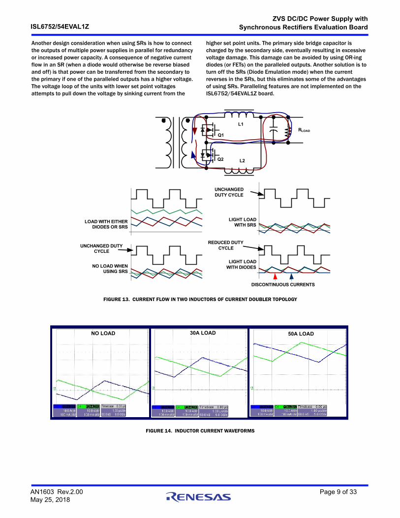
Current Doubler Figure 13 on page 9 illustrates the current flow in the two inductors of the current doubler topology. Current flow in the circuit is correlated with the waveforms by color coding. The green waveform represents the sum of red and blue currents through RLOAD. For circuit clarity, paralleled SRs and output capacitors of the ISL6752/54EVAL1Z board are not shown.
When using diodes (instead of SRs), if the average load current is less than half of the ramp current in the output inductors, the current in the inductors becomes discontinuous, and the duty cycle of the PWM is shortened to maintain the desired output voltage.
When using SRs, the inductor currents in L1 and L2 can become negative because current in SRs can flow bidirectionally; consequently, the duty cycle remains virtually unchanged. The benefit is that the load transient performance is the same for any load from zero up to current limit. Another advantage is that, for very light loads, the duty cycle is not reduced to very small duty cycles, pulse skipping does not occur, and the associated voltage jitter does not occur.
When designing the current doubler topology, the DC resistance of both halves must be equal. The PCB layout must be as symmetrical as possible, and the DCRs of the inductors should be reasonably equal. If not, the current between the two sides does not split equally. Because perfect physical PCB symmetry is not always possible, current sharing between inductors must be confirmed.
In Figure 14 on page 9, inductor current waveforms are taken from the ISL6752/54EVAL1Z board. Current balance between the two inductors was achieved after one board revision. The inductor currents maintain the same waveform shape even at no load.
R27
U4
U4
V1
V1
V2
ENABLE
R-SR
LSR
V4
V3
T6
OUTLLN
OUTLRNLLN
LRN
LLN
PWM
ISL89163
D9
C10C9
R28
/OUTLRN V2
/OUTLLN
L R L
V3
V4
LRN
VBIAS
Q100
Q101
EL7212
Red dashed lines point out the turn-on delay of the SRs when PWM goes low
C123
FIGURE 12. SIMPLIFIED SR DRIVE SCHEMATIC
AN1603 Rev.2.00 Page 8 of 33May 25, 2018
ISL6752/54EVAL1Z ZVS DC/DC Power Supply with
Synchronous Rectifiers Evaluation Board
Another design consideration when using SRs is how to connect the outputs of multiple power supplies in parallel for redundancy or increased power capacity. A consequence of negative current flow in an SR (when a diode would otherwise be reverse biased and off) is that power can be transferred from the secondary to the primary if one of the paralleled outputs has a higher voltage. The voltage loop of the units with lower set point voltages attempts to pull down the voltage by sinking current from the
higher set point units. The primary side bridge capacitor is charged by the secondary side, eventually resulting in excessive voltage damage. This damage can be avoided by using OR-ing diodes (or FETs) on the paralleled outputs. Another solution is to turn off the SRs (Diode Emulation mode) when the current reverses in the SRs, but this eliminates some of the advantages of using SRs. Paralleling features are not implemented on the ISL6752/54EVAL1Z board.
L1
L2
Q1
Q2
RLOAD
NO LOAD WHEN USING SRS
LOAD WITH EITHER DIODES OR SRS
LIGHT LOAD WITH SRS
LIGHT LOAD WITH DIODES
REDUCED DUTY CYCLE
UNCHANGED DUTY CYCLE
UNCHANGED DUTY CYCLE
DISCONTINUOUS CURRENTS
FIGURE 13. CURRENT FLOW IN TWO INDUCTORS OF CURRENT DOUBLER TOPOLOGY
FIGURE 14. INDUCTOR CURRENT WAVEFORMS
50A LOAD30A LOADNO LOAD
AN1603 Rev.2.00 Page 9 of 33May 25, 2018
ISL6752/54EVAL1Z ZVS DC/DC Power Supply with
Synchronous Rectifiers Evaluation Board
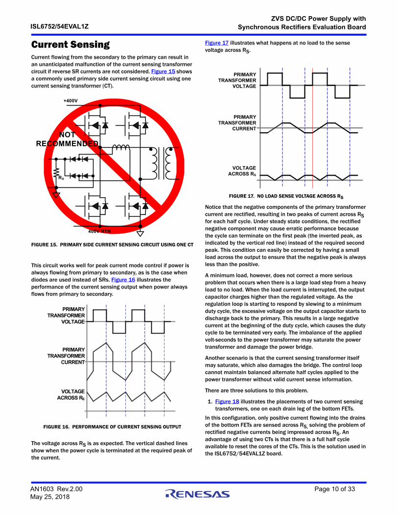
Current SensingCurrent flowing from the secondary to the primary can result in an unanticipated malfunction of the current sensing transformer circuit if reverse SR currents are not considered. Figure 15 shows a commonly used primary side current sensing circuit using one current sensing transformer (CT).
This circuit works well for peak current mode control if power is always flowing from primary to secondary, as is the case when diodes are used instead of SRs. Figure 16 illustrates the performance of the current sensing output when power always flows from primary to secondary.
The voltage across RS is as expected. The vertical dashed lines show when the power cycle is terminated at the required peak of the current.
Figure 17 illustrates what happens at no load to the sense voltage across RS.
Notice that the negative components of the primary transformer current are rectified, resulting in two peaks of current across RS for each half cycle. Under steady state conditions, the rectified negative component may cause erratic performance because the cycle can terminate on the first peak (the inverted peak, as indicated by the vertical red line) instead of the required second peak. This condition can easily be corrected by having a small load across the output to ensure that the negative peak is always less than the positive.
A minimum load, however, does not correct a more serious problem that occurs when there is a large load step from a heavy load to no load. When the load current is interrupted, the output capacitor charges higher than the regulated voltage. As the regulation loop is starting to respond by slewing to a minimum duty cycle, the excessive voltage on the output capacitor starts to discharge back to the primary. This results in a large negative current at the beginning of the duty cycle, which causes the duty cycle to be terminated very early. The imbalance of the applied volt-seconds to the power transformer may saturate the power transformer and damage the power bridge.
Another scenario is that the current sensing transformer itself may saturate, which also damages the bridge. The control loop cannot maintain balanced alternate half cycles applied to the power transformer without valid current sense information.
There are three solutions to this problem.
1. Figure 18 illustrates the placements of two current sensing transformers, one on each drain leg of the bottom FETs.
In this configuration, only positive current flowing into the drains of the bottom FETs are sensed across RS, solving the problem of rectified negative currents being impressed across RS. An advantage of using two CTs is that there is a full half cycle available to reset the cores of the CTs. This is the solution used in the ISL6752/54EVAL1Z board.
+400V
400V RTN
RS
NOT RECOMMENDED
FIGURE 15. PRIMARY SIDE CURRENT SENSING CIRCUIT USING ONE CT
PRIMARY TRANSFORMER
VOLTAGE
PRIMARY TRANSFORMER
CURRENT
VOLTAGE ACROSS RS
FIGURE 16. PERFORMANCE OF CURRENT SENSING OUTPUT
PRIMARY TRANSFORMER
VOLTAGE
PRIMARY TRANSFORMER
CURRENT
VOLTAGE ACROSS RS
FIGURE 17. NO LOAD SENSE VOLTAGE ACROSS RS
AN1603 Rev.2.00 Page 10 of 33May 25, 2018
ISL6752/54EVAL1Z ZVS DC/DC Power Supply with
Synchronous Rectifiers Evaluation Board
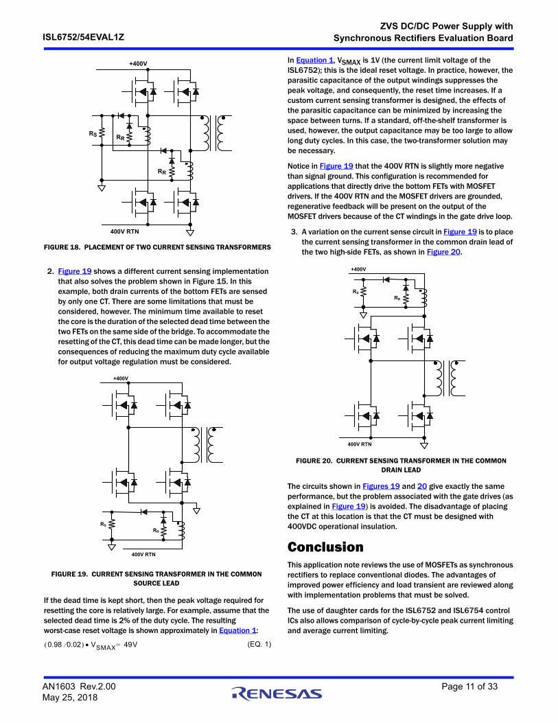
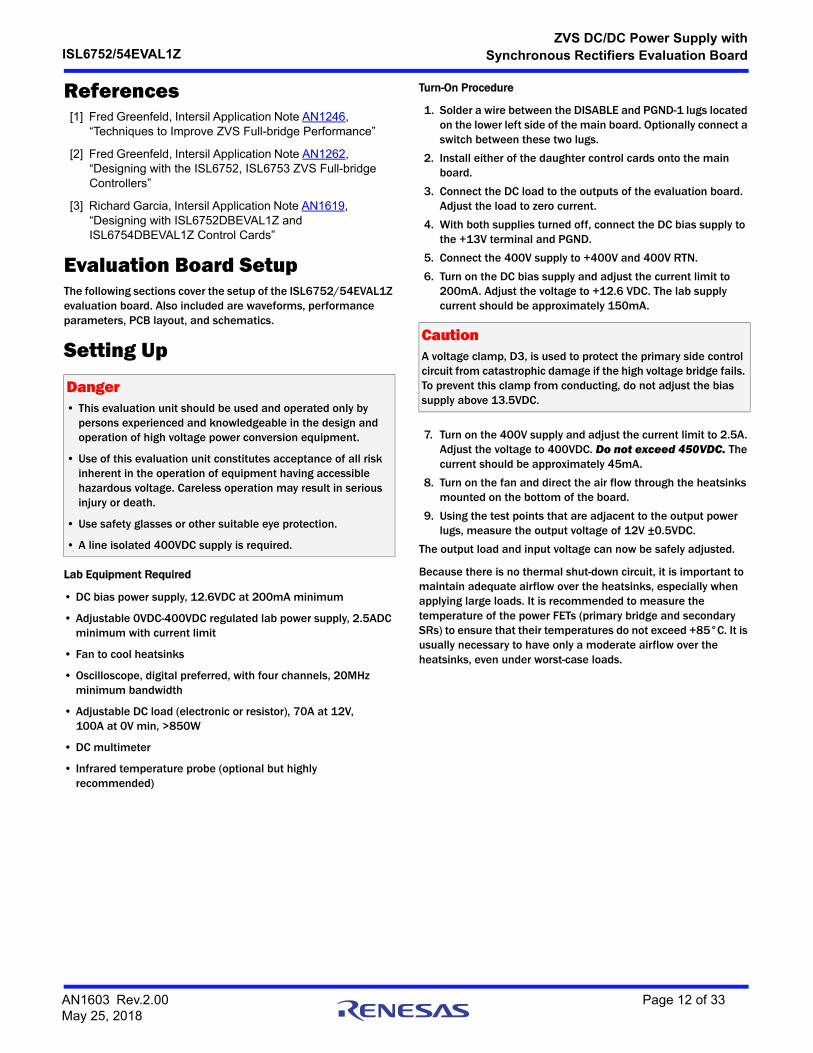
2. Figure 19 shows a different current sensing implementation that also solves the problem shown in Figure 15. In this example, both drain currents of the bottom FETs are sensed by only one CT. There are some limitations that must be considered, however. The minimum time available to reset the core is the duration of the selected dead time between the two FETs on the same side of the bridge. To accommodate the resetting of the CT, this dead time can be made longer, but the consequences of reducing the maximum duty cycle available for output voltage regulation must be considered.
If the dead time is kept short, then the peak voltage required for resetting the core is relatively large. For example, assume that the selected dead time is 2% of the duty cycle. The resulting worst-case reset voltage is shown approximately in Equation 1:
In Equation 1, VSMAX is 1V (the current limit voltage of the ISL6752); this is the ideal reset voltage. In practice, however, the parasitic capacitance of the output windings suppresses the peak voltage, and consequently, the reset time increases. If a custom current sensing transformer is designed, the effects of the parasitic capacitance can be minimized by increasing the space between turns. If a standard, off-the-shelf transformer is used, however, the output capacitance may be too large to allow long duty cycles. In this case, the two-transformer solution may be necessary.
Notice in Figure 19 that the 400V RTN is slightly more negative than signal ground. This configuration is recommended for applications that directly drive the bottom FETs with MOSFET drivers. If the 400V RTN and the MOSFET drivers are grounded, regenerative feedback will be present on the output of the MOSFET drivers because of the CT windings in the gate drive loop.
3. A variation on the current sense circuit in Figure 19 is to place the current sensing transformer in the common drain lead of the two high-side FETs, as shown in Figure 20.
The circuits shown in Figures 19 and 20 give exactly the same performance, but the problem associated with the gate drives (as explained in Figure 19) is avoided. The disadvantage of placing the CT at this location is that the CT must be designed with 400VDC operational insulation.
ConclusionThis application note reviews the use of MOSFETs as synchronous rectifiers to replace conventional diodes. The advantages of improved power efficiency and load transient are reviewed along with implementation problems that must be solved.
The use of daughter cards for the ISL6752 and ISL6754 control ICs also allows comparison of cycle-by-cycle peak current limiting and average current limiting.
+400V
400V RTN
RS RR
RR
FIGURE 18. PLACEMENT OF TWO CURRENT SENSING TRANSFORMERS
FIGURE 19. CURRENT SENSING TRANSFORMER IN THE COMMON SOURCE LEAD
400V RTN
+400V
RS
RR
0.98 0.02 VSMAX 49V= (EQ. 1)
+400V
RS
RR
400V RTN
FIGURE 20. CURRENT SENSING TRANSFORMER IN THE COMMON DRAIN LEAD
AN1603 Rev.2.00 Page 11 of 33May 25, 2018
ISL6752/54EVAL1Z ZVS DC/DC Power Supply with
Synchronous Rectifiers Evaluation Board
References[1] Fred Greenfeld, Intersil Application Note AN1246,
“Techniques to Improve ZVS Full-bridge Performance”
[2] Fred Greenfeld, Intersil Application Note AN1262, “Designing with the ISL6752, ISL6753 ZVS Full-bridge Controllers”
[3] Richard Garcia, Intersil Application Note AN1619, “Designing with ISL6752DBEVAL1Z and ISL6754DBEVAL1Z Control Cards”
Evaluation Board SetupThe following sections cover the setup of the ISL6752/54EVAL1Z evaluation board. Also included are waveforms, performance parameters, PCB layout, and schematics.
Setting Up
Lab Equipment Required
• DC bias power supply, 12.6VDC at 200mA minimum
• Adjustable 0VDC-400VDC regulated lab power supply, 2.5ADC minimum with current limit
• Fan to cool heatsinks
• Oscilloscope, digital preferred, with four channels, 20MHz minimum bandwidth
• Adjustable DC load (electronic or resistor), 70A at 12V, 100A at 0V min, >850W
• DC multimeter
• Infrared temperature probe (optional but highly recommended)
Turn-On Procedure
1. Solder a wire between the DISABLE and PGND-1 lugs located on the lower left side of the main board. Optionally connect a switch between these two lugs.
2. Install either of the daughter control cards onto the main board.
3. Connect the DC load to the outputs of the evaluation board. Adjust the load to zero current.
4. With both supplies turned off, connect the DC bias supply to the +13V terminal and PGND.
5. Connect the 400V supply to +400V and 400V RTN.
6. Turn on the DC bias supply and adjust the current limit to 200mA. Adjust the voltage to +12.6 VDC. The lab supply current should be approximately 150mA.
7. Turn on the 400V supply and adjust the current limit to 2.5A. Adjust the voltage to 400VDC. Do not exceed 450VDC. The current should be approximately 45mA.
8. Turn on the fan and direct the air flow through the heatsinks mounted on the bottom of the board.
9. Using the test points that are adjacent to the output power lugs, measure the output voltage of 12V ±0.5VDC.
The output load and input voltage can now be safely adjusted.
Because there is no thermal shut-down circuit, it is important to maintain adequate airflow over the heatsinks, especially when applying large loads. It is recommended to measure the temperature of the power FETs (primary bridge and secondary SRs) to ensure that their temperatures do not exceed +85°C. It is usually necessary to have only a moderate airflow over the heatsinks, even under worst-case loads.
Danger• This evaluation unit should be used and operated only by
persons experienced and knowledgeable in the design and operation of high voltage power conversion equipment.
• Use of this evaluation unit constitutes acceptance of all risk inherent in the operation of equipment having accessible hazardous voltage. Careless operation may result in serious injury or death.
• Use safety glasses or other suitable eye protection.
• A line isolated 400VDC supply is required.
CautionA voltage clamp, D3, is used to protect the primary side control circuit from catastrophic damage if the high voltage bridge fails. To prevent this clamp from conducting, do not adjust the bias supply above 13.5VDC.
AN1603 Rev.2.00 Page 12 of 33May 25, 2018
ISL6752/54EVAL1Z ZVS DC/DC Power Supply with
Synchronous Rectifiers Evaluation Board
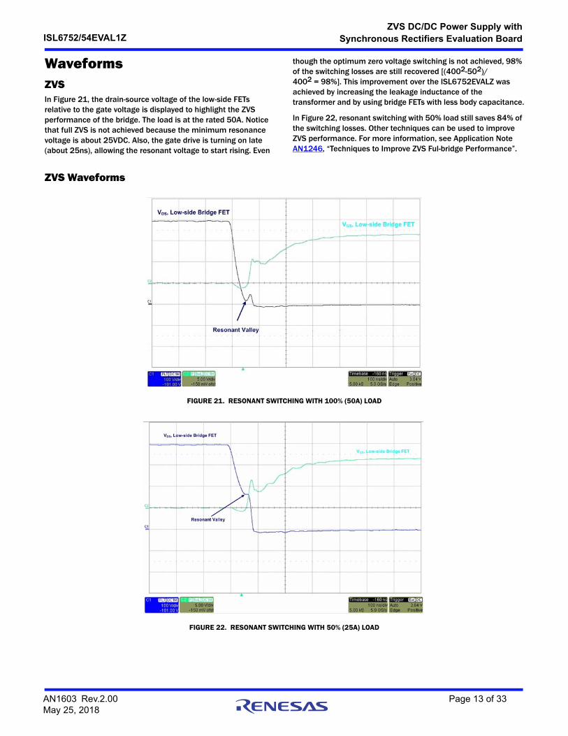
WaveformsZVS In Figure 21, the drain-source voltage of the low-side FETs relative to the gate voltage is displayed to highlight the ZVS performance of the bridge. The load is at the rated 50A. Notice that full ZVS is not achieved because the minimum resonance voltage is about 25VDC. Also, the gate drive is turning on late (about 25ns), allowing the resonant voltage to start rising. Even
though the optimum zero voltage switching is not achieved, 98% of the switching losses are still recovered [(4002-502)/4002 = 98%]. This improvement over the ISL6752EVALZ was achieved by increasing the leakage inductance of the transformer and by using bridge FETs with less body capacitance.
In Figure 22, resonant switching with 50% load still saves 84% of the switching losses. Other techniques can be used to improve ZVS performance. For more information, see Application Note AN1246, “Techniques to Improve ZVS Ful-bridge Performance”.
ZVS Waveforms
FIGURE 21. RESONANT SWITCHING WITH 100% (50A) LOAD
FIGURE 22. RESONANT SWITCHING WITH 50% (25A) LOAD
AN1603 Rev.2.00 Page 13 of 33May 25, 2018
ISL6752/54EVAL1Z ZVS DC/DC Power Supply with
Synchronous Rectifiers Evaluation Board
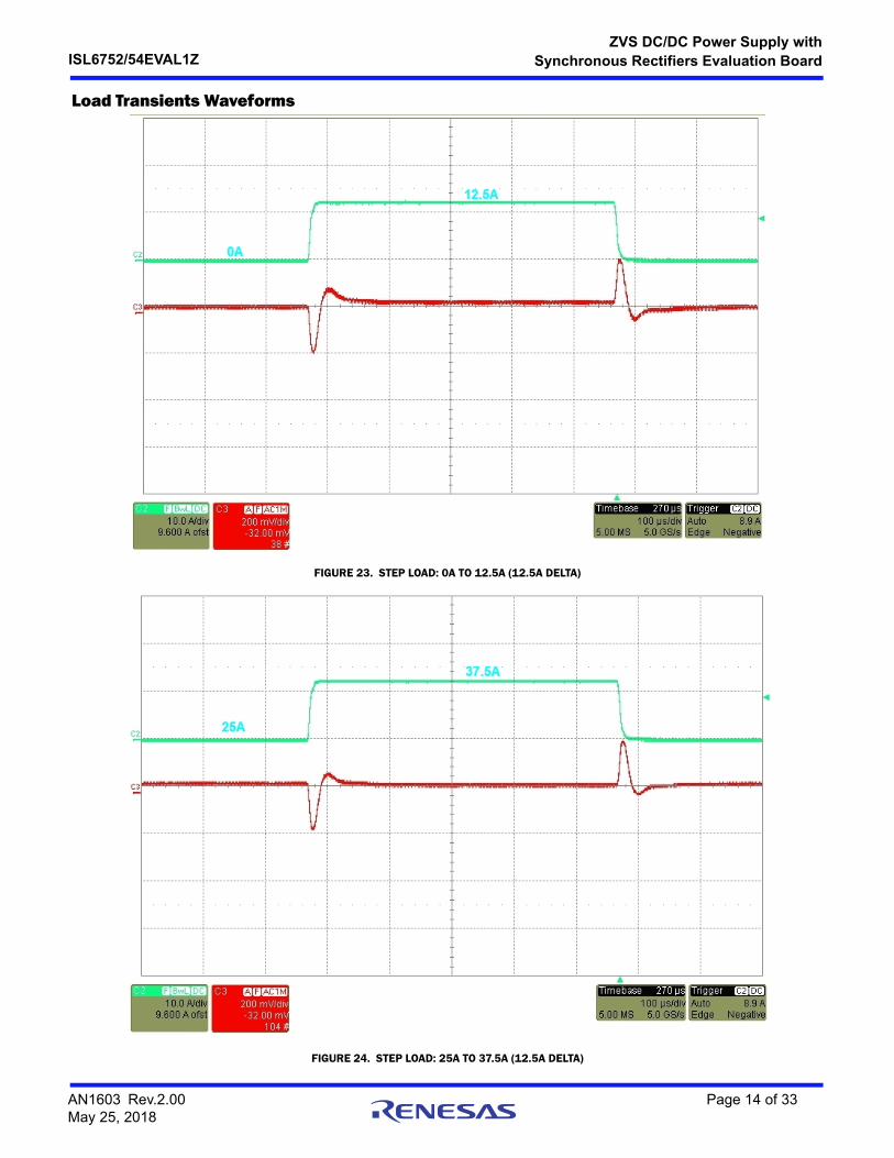
Load Transients Waveforms
FIGURE 23. STEP LOAD: 0A TO 12.5A (12.5A DELTA)
FIGURE 24. STEP LOAD: 25A TO 37.5A (12.5A DELTA)
AN1603 Rev.2.00 Page 14 of 33May 25, 2018
ISL6752/54EVAL1Z ZVS DC/DC Power Supply with
Synchronous Rectifiers Evaluation Board
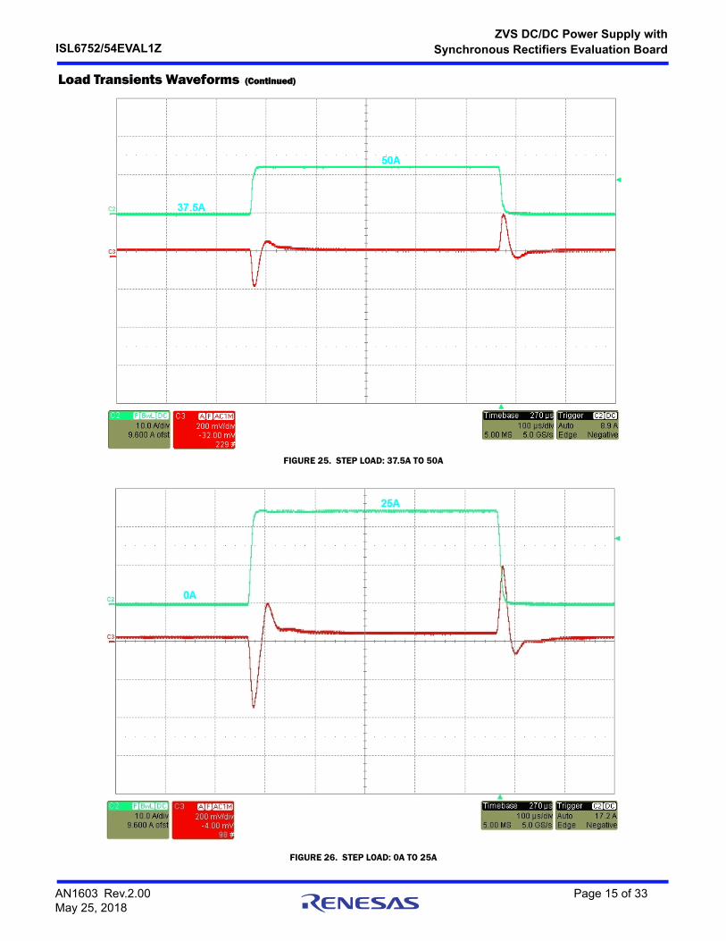
FIGURE 25. STEP LOAD: 37.5A TO 50A
FIGURE 26. STEP LOAD: 0A TO 25A
Load Transients Waveforms (Continued)
AN1603 Rev.2.00 Page 15 of 33May 25, 2018
ISL6752/54EVAL1Z ZVS DC/DC Power Supply with
Synchronous Rectifiers Evaluation Board
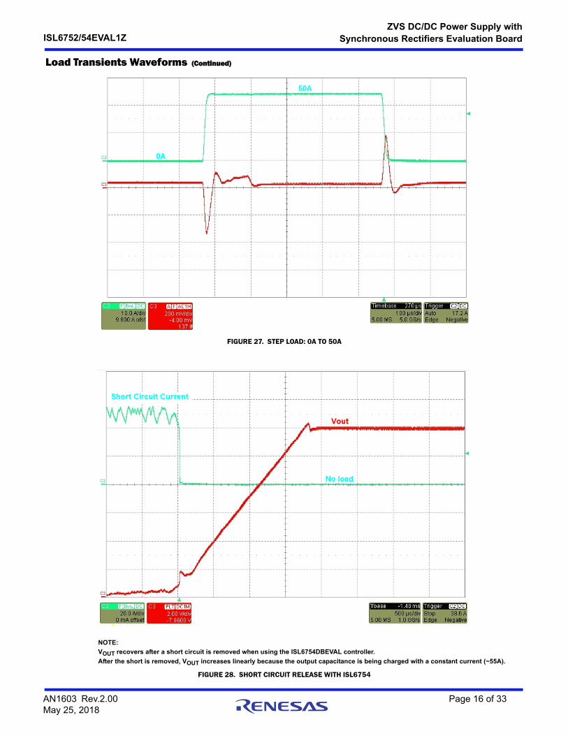
FIGURE 27. STEP LOAD: 0A TO 50A
FIGURE 28. SHORT CIRCUIT RELEASE WITH ISL6754
Load Transients Waveforms (Continued)
VOUT recovers after a short circuit is removed when using the ISL6754DBEVAL controller.
After the short is removed, VOUT increases linearly because the output capacitance is being charged with a constant current (~55A).
NOTE:
AN1603 Rev.2.00 Page 16 of 33May 25, 2018
ISL6752/54EVAL1Z ZVS DC/DC Power Supply with
Synchronous Rectifiers Evaluation Board
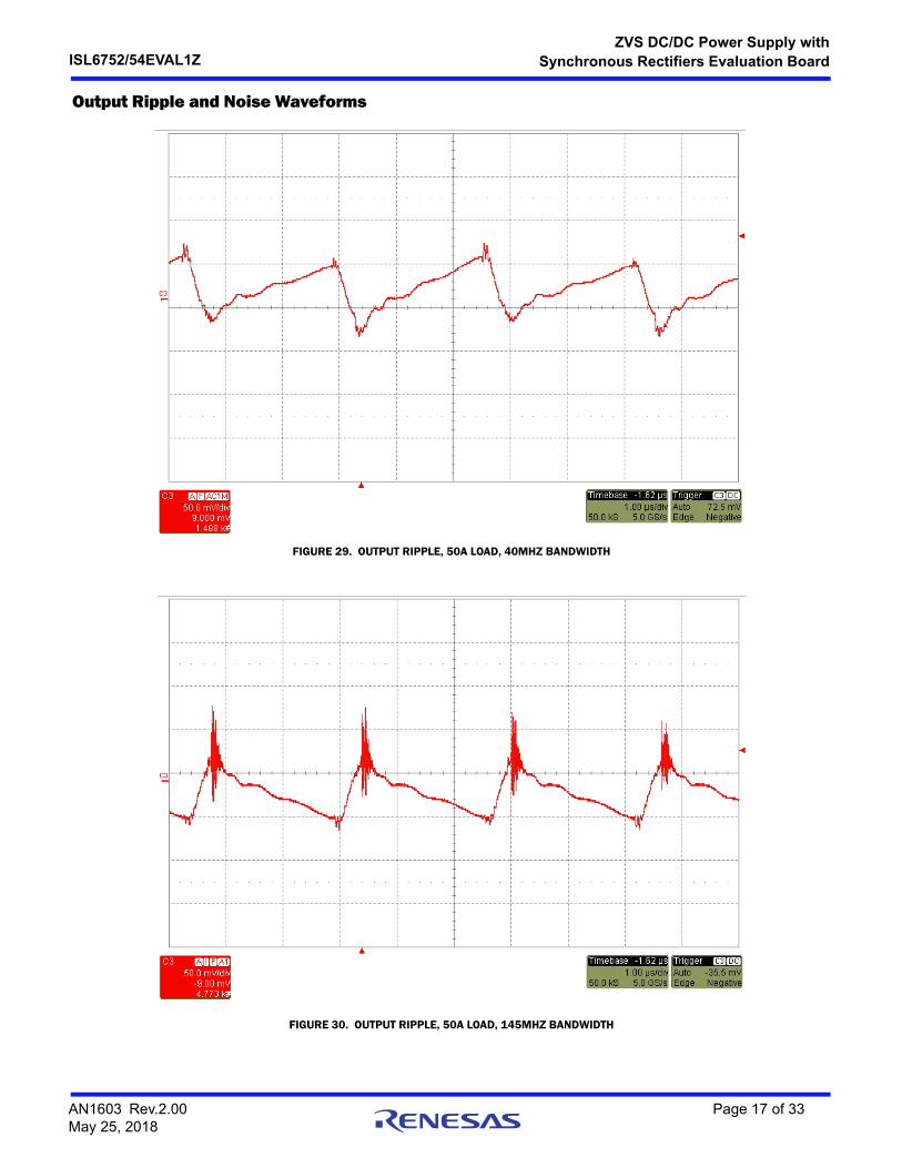
Output Ripple and Noise Waveforms
FIGURE 29. OUTPUT RIPPLE, 50A LOAD, 40MHZ BANDWIDTH
FIGURE 30. OUTPUT RIPPLE, 50A LOAD, 145MHZ BANDWIDTH
AN1603 Rev.2.00 Page 17 of 33May 25, 2018
ISL6752/54EVAL1Z ZVS DC/DC Power Supply with
Synchronous Rectifiers Evaluation Board
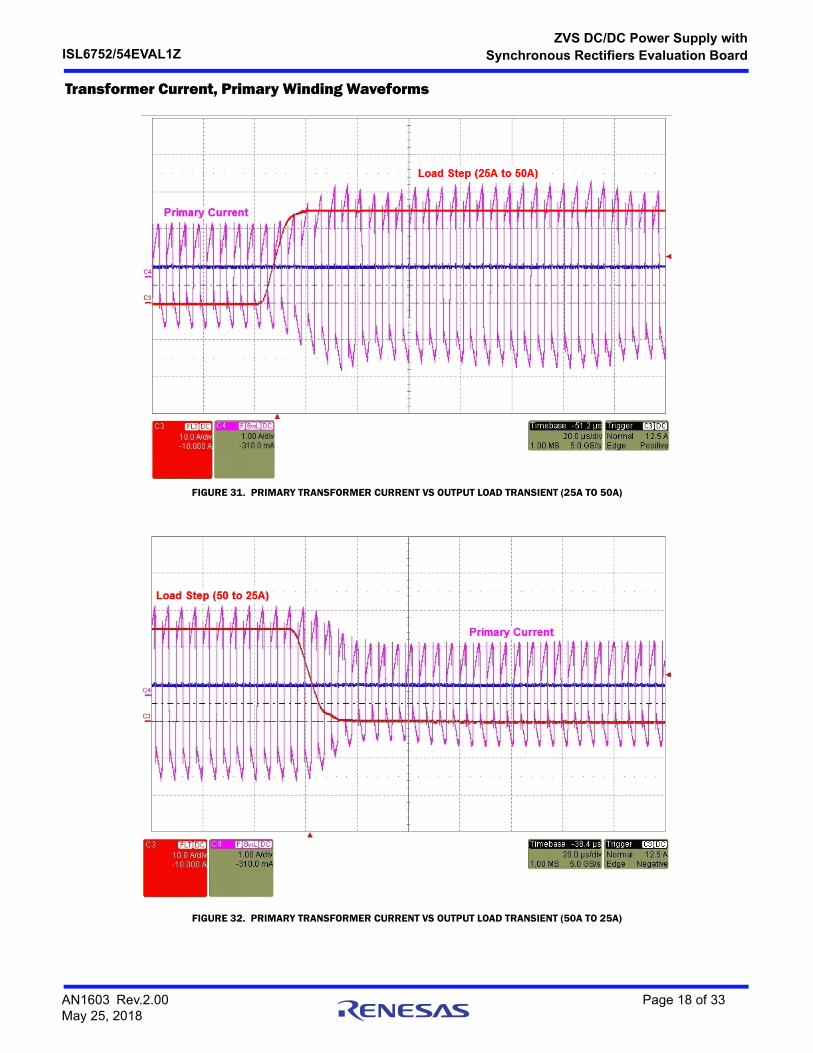
Transformer Current, Primary Winding Waveforms
FIGURE 31. PRIMARY TRANSFORMER CURRENT VS OUTPUT LOAD TRANSIENT (25A TO 50A)
FIGURE 32. PRIMARY TRANSFORMER CURRENT VS OUTPUT LOAD TRANSIENT (50A TO 25A)
AN1603 Rev.2.00 Page 18 of 33May 25, 2018
ISL6752/54EVAL1Z ZVS DC/DC Power Supply with
Synchronous Rectifiers Evaluation Board
Performance Curves
FIGURE 33. POWER EFFICIENCY VS LOAD (ISL6752 OR ISL6754)
FIGURE 34. LOAD REGULATION FIGURE 35. PULSE BY PULSE VS AVERAGE CURRENT LIMIT
0 2 10 15 20 25
70
75
80
85
909295
100
OUTPUT CURRENT (A)
EF
FIC
IEN
CY
(%
)65
60
55
5030 35 40 45 50 55
92% EFFICIENCYWITH 20% LOAD
12.00
11.95
11.90
11.85
11.80
ISL6754
ISL6752
0 10 20 30 40 50 60IOUT (A)
VO
UT (
V)
0 10 20 30 40 50 60 70 80
IOUT (A)
VO
UT (
V)
12
10
8
6
4
2
0
ISL6754
ISL6752
AN1603 Rev.2.00 Page 19 of 33May 25, 2018
AN
16
03R
ev.2
.00
Pa
ge 2
0 of 33
May 25
, 201
8
ISL6
752
/54E
VA
L1
Z
SR_EN144
R25R145U4
C11 C10
R23
Q100
C123
C9
R26R29
C133
D10
R140
R27R143
D9
R139
R28Q101
D11
C136
12V_RTN
P103
P104
R148
+12VOUTC132
VOUT
C135
C134+
+
+
+
OPERATION MAY RESULT IN SERIOUS INJURY OR DEATH.- USE SAFTY GLASSES OR OTHER SUITABLE EYE PROTECTION.
EQUIPMENT.- USE OF THIS EVALUATION UNIT CONSTITUTES ACCEPTANCE
OF ALL RISKS INHERENT IN THE OPERATION OF EQUIPMENTHAVING ACCESSIBLE HAZARDOUS VOLTAGES. CARELESS
- THIS EVALUATION UNIT SHOULD BE USED AND OPERATEDONLY BY PERSONS EXPERIENCED AND KNOWLEDGEABLE IN THEDESIGN AND OPERATION OF HIGH VOLTAGE POWER CONVERSION
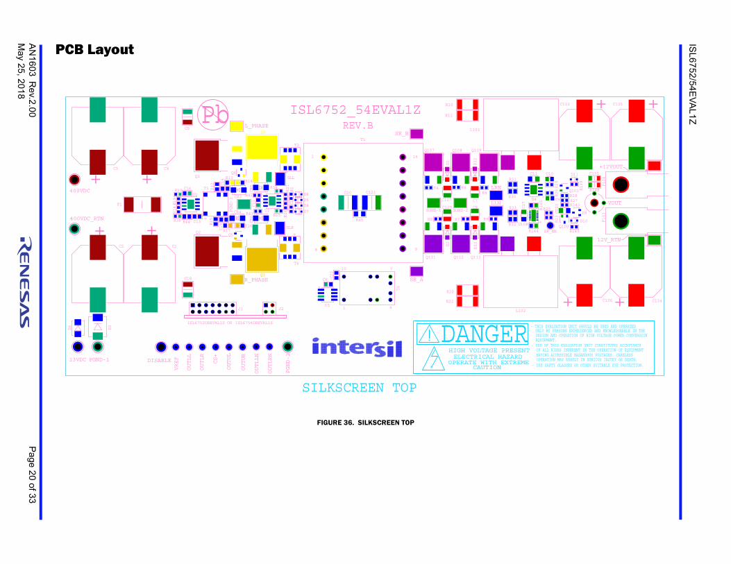
PCB Layout
FIGURE 36. SILKSCREEN TOP
13VDC
D4
400VDC_RTN
400VDC
PGND-1
D3
C2
F1
C3
DISABLE
C4
OUTLL
VREF
ISL6752DBEVAL1Z OR
C18
C1
R36 R44
R18R19
R37 C16
C5
OUTLR
Q2
C13
R15
T3 R12
U2
Q1
OUTUL
CS+
Q5
C15
R17PGND-3
C14 R13
OUTUR
ISL6754DBEVAL1Z
J1
R_PHASE
R16
CR6
R43CR4
R42
R14
CR3
CR5
Q6
L_PHASE
OUTLRN
OUTLLN
C12
U1
PGND-2
J2
GLR
R24
R3
R35
R21R34
GLL
T4
D5
D7D8
D6
R2
T2
U3
C6 C22
C20
R45
C121
T1
T6
SR_B
SR_A
Q111
R5
SGND-1
Q107
R22
R20
D2
C127
C129
R4
D1
R10
R11
Q112
R7
SGND-2
R6
Q108
D13
Q113
R9
C7
C8
R8
D12
Q109
L103
LLN
LRN
L102
U108R32
C17
R33
R30
R31
R
+
+
+
+
Pb ISL6752_54EVAL1Z
8
1
1
10
REV.B
4
7
9
16
SILKSCREEN TOP
OPERATE WITH EXTREME
DANGERHIGH VOLTAGE PRESENTELECTRICAL HAZARD
CAUTION
Q3
Q4
AN
16
03R
ev.2
.00
Pa
ge 2
1 of 33
May 25
, 201
8
ISL6
752
/54E
VA
L1
Z
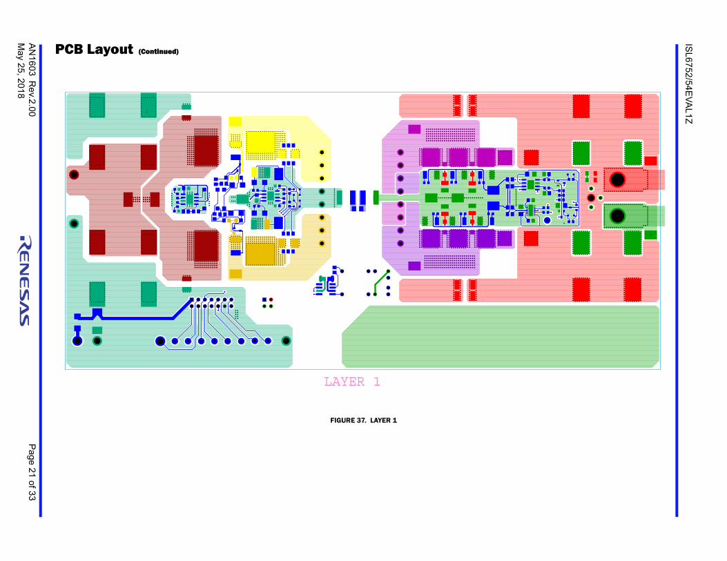
FIGURE 37. LAYER 1
PCB Layout (Continued)
LAYER 1
AN
16
03R
ev.2
.00
Pa
ge 2
2 of 33
May 25
, 201
8
ISL6
752
/54E
VA
L1
Z
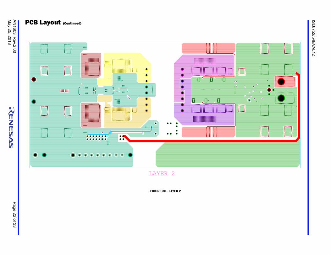
FIGURE 38. LAYER 2
PCB Layout (Continued)
LAYER 2
AN
16
03R
ev.2
.00
Pa
ge 2
3 of 33
May 25
, 201
8
ISL6
752
/54E
VA
L1
Z
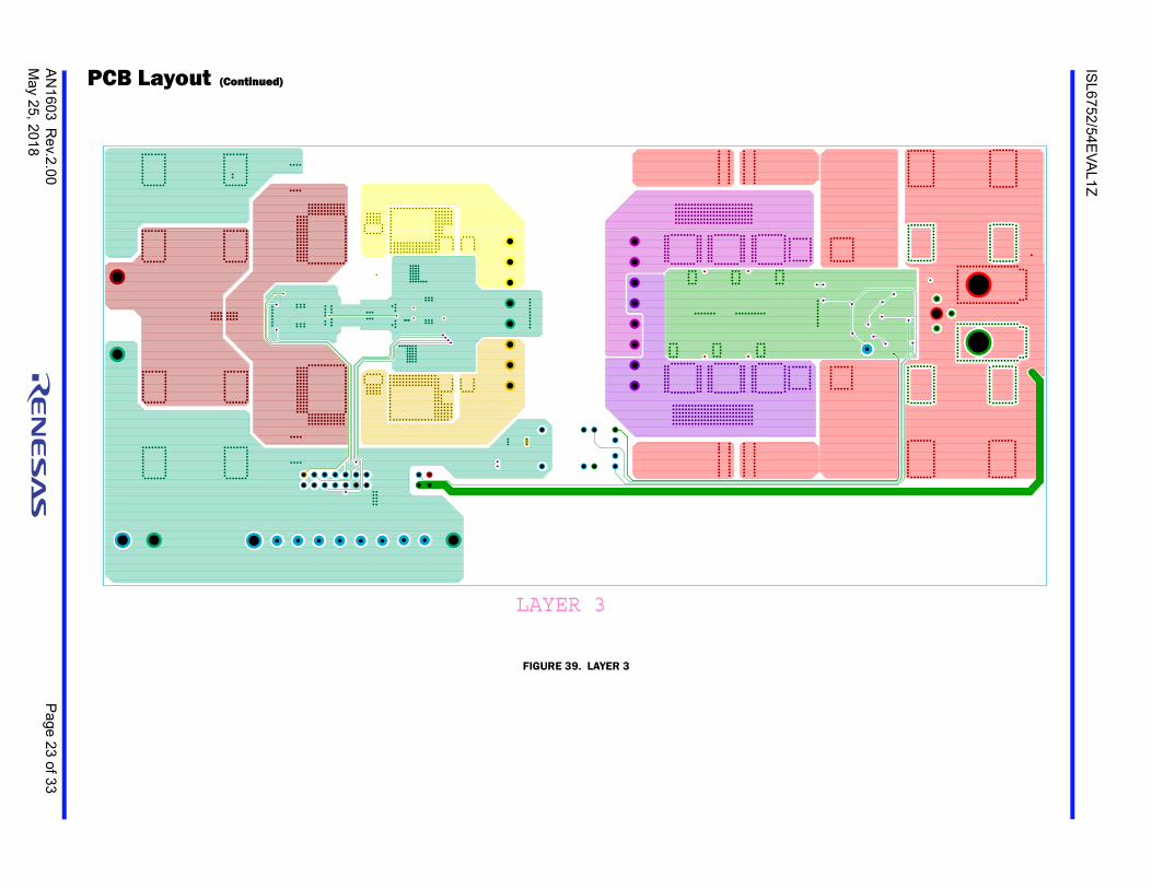
FIGURE 39. LAYER 3
PCB Layout (Continued)
LAYER 3
AN
16
03R
ev.2
.00
Pa
ge 2
4 of 33
May 25
, 201
8
ISL6
752
/54E
VA
L1
Z
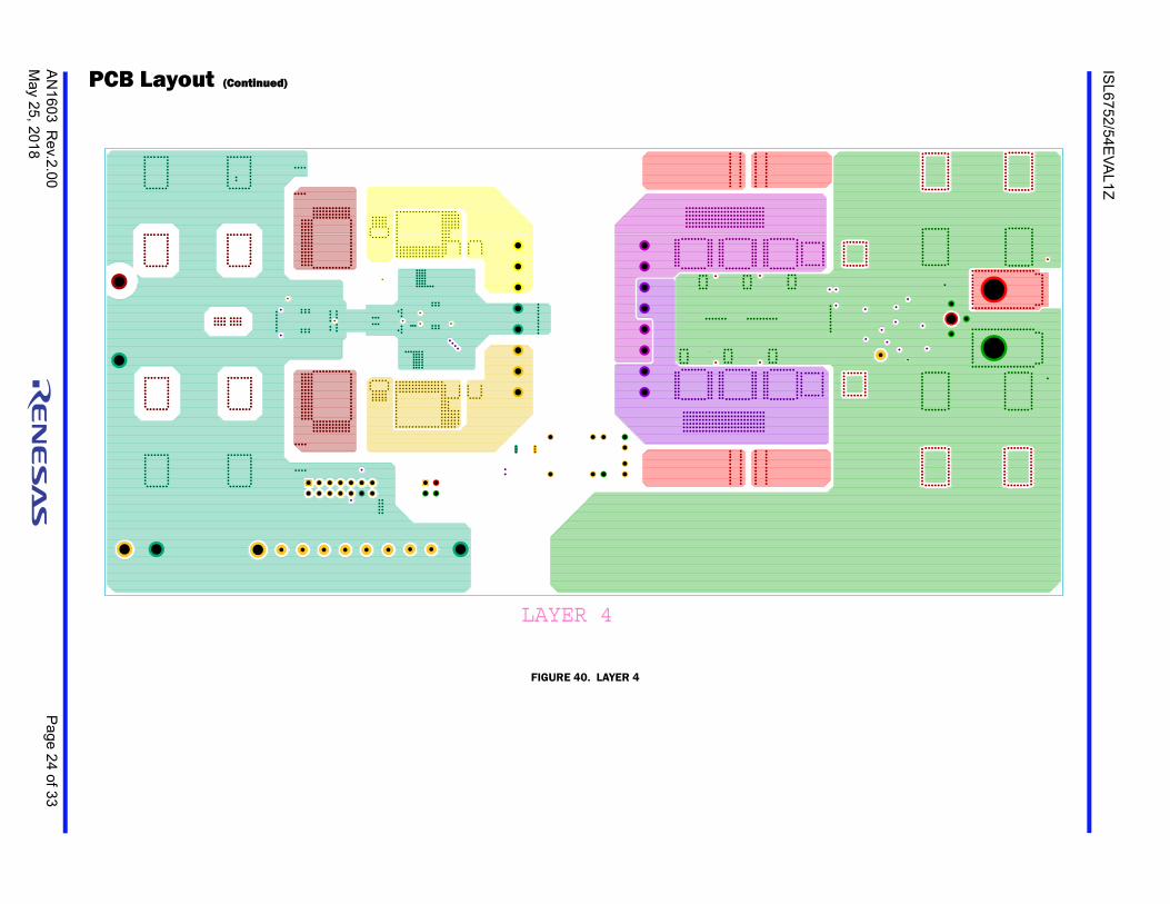
FIGURE 40. LAYER 4
PCB Layout (Continued)
LAYER 4
AN
16
03R
ev.2
.00
Pa
ge 2
5 of 33
May 25
, 201
8
ISL6
752
/54E
VA
L1
Z
1650
9
1615
1413
1211
10
T1
CHARD GARCIA 08/03
SR_B
SR_AOUT
OUT
DATE:
600W12V
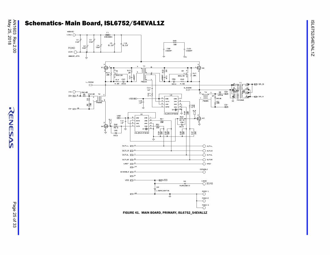
Schematics- Main Board, ISL6752/54EVAL1Z
FIGURE 41. MAIN BOARD, PRIMARY, ISL6752_54EVAL1Z
PGND
1000PF
J1CS- 10
CR5
SS12
49.9
R421UFC12
C16VDD
R44
4.7
1UFC13
7
8 1
3
T4
P8205
R37
10K
OUTUR
OUTUL
10K
R36
OUTLL
OUTLR
10K
R35
10K
R34
GLL
VDD
5
4
C233UF
C3
0464004
F1
C50.1UF
C180.1UF
33UFC4
33UFC1
33UF
VIN+
VIN-
6
D6 1P8205
8
3
PA
1N4148
2
MURS160T3
3J1
1.5SMC15AT3G
VDD
D3
3
1
2
Q2
CS+
D71N4148
8
76
4
32
3
10K
6
ISL89163FBEBZ
1
R1220
C14
VDD
DISABLE
BIAS
100
CS+
3300PF
4.99
BSS138
1000
PF
SS12
10K
4.99
3
2
R13
R14 CR3 R16
C15R1
5 3
1
2
C121
D4
R45
T3
8
1
6
3
7
DISABLE
OUTUR
OUTUL
OUTLR
J1 1
J1 14
J1
4
J1 5
J1
7
J1 12
21
3
U1
8
3
27
1
3
2
4
7
5
CR6
100
J1
J1
2
8J1
5
Q5
9
2
1
U2
CS+T2
9
R19
5
1
R214
6
Q4
J1
VREF
PGND-3
8
R43
R18
R3
9
OUTLL
1UF
P0544
1N4148
400VDC
VREF
D8
C20
Q3
SS12
CS-
100
R17
PGND-2
PGND-1
13VDC
100
SS12
1
BSS138
Q6
RI
L_PHASE
R241
ISL89163FBEBZ 100
GLR
100
20
R_PHASE
CR4
3300PF
49.9
Q1
400VDC_RTN
D5 1N4148
3
100
R2
OUT
IN
OUT
IN
DRAWN BY:
OUT
ENB
VDD
EP
GND
OUTB INB
OUTA INA
ENA
ENB
VDD
EP
GND
OUTB INB
OUTA INA
ENA
200KHZ
NC
NCNCNC
300-400V
E
AN
16
03R
ev.2
.00
Pa
ge 2
6 of 33
May 25
, 201
8
ISL6
752
/54E
VA
L1
Z
P103
R144
0
0
4.7U
F
DNP
1K
DNP
10K
P104R148
VOUT
LLN
R145
R32
R33
R30
R31
LRNLRN
LLN
+12VOUT
12V_RTN
SGND-1
SGND-2
10K
4.7U
FC1
7
10VVCC_BAR
E
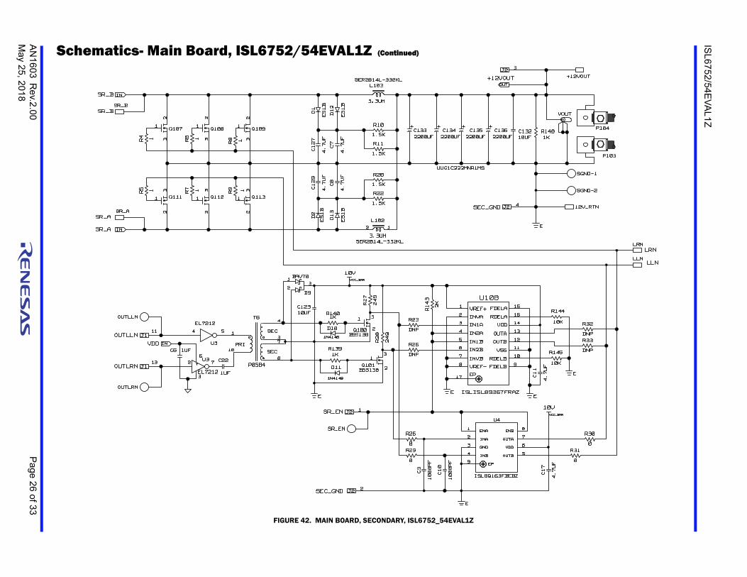
FIGURE 42. MAIN BOARD, SECONDARY, ISL6752_54EVAL1Z
Schematics- Main Board, ISL6752/54EVAL1Z (Continued)
SEC_GND
SEC_GND
SER2814L-332KLL103
13
11
1N4148
D11
D9
BAV701
23
10V
R1401K
1N4148
D10
R1391K
C12310UF
1
BSS138Q100
249
R27
2
3
Q101BSS138
13
2
R28
249OUTLLN
VDD
U3 C22P0584
SR_EN
ES1B
1
2
D2
SR_B
31
SR_A
1.5K
16
3
R143
R9
SER2814L-332KL
1
ISL89163FBEBZ
6
SR_EN
4.7U
F
ES1B
DNP
R25
EL7212
C6
J2
J1
SR_A
3
Q111
OUTLLN
OUTLRN
5
310
00PF
2200UF
DNP
2K0
3.3UH
4.7U
F
4.7U
F 1.5K
1.5K
1.5K
3.3UH
2200UF
ES1B
1UF
2200UF
1
11
ES1B
1
SR_B
C132C134 C135C133
3
2 76
4 5
SR_B
SR_A
L10212
4
73
D1 D12
D13
4
2
7
15
14
8
J2 2
3
J1
R4 R6 R8
R5 R7
2
1
3
Q108
2
1
3
Q1091
2
1 Q112
2
1
3
1
3
C127 C7
C8
R26
R29
R10
R11
R20
U4
1 8
9
2
4
7
5
C9 C10
Q107
R22
C129
Q113
4.7U
F
+12VOUTJ2
4J2
2200UFC136
10UF
10
T6
1
1000
PF
1
U108
EL7212
0
2
OUTLRN
8
10
U3
1UF
9
11
12
13
C11
UUG1C222MNR1MS
R23
6
17
ISLISL89367FRAZ
OUT
IN
IN
IN
EE
E
ENB
VDD
EP
GND
OUTBINB
OUTAINA
ENA
VREF- FDELB
RDELB
VDD
IN2A
IN1B OUTB
VSS
EP
VREF+ FDELA
IN2B
RDELA
INVB
OUTA
IN1A
INVA
VCC_BAR
E
E
PRI
SEC
SEC
AN
16
03R
ev.2
.00
Pa
ge 2
7 of 33
May 25
, 201
8
ISL6
752
/54E
VA
L1
Z
BETWEENTHIS PAD
RICHARD_GA
OUTLRN
OURLLN
OUTUL
OUTUR
OUTLR
OUTLL
13
100P
F
C17
J13
J15
J17
J19
J111
J1
PGND
TP_PRI
LEASED BY:
AWN BY:
DATED BY:
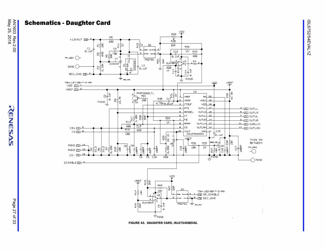
Schematics - Daughter Card
FIGURE 43. DAUGHTER CARD, ISL6754DBEVAL
CS-
ISL6754AAZA
VREF
10K
VREF
U4
1
10 11
12
13
14
15
16
17
18
192
20
3
4
5
6
7
8
9
3.48
K
R20
DNP
BZX8
4C6V
8LT1
DNP
EL5120IWT
PGND
1K
DISABLE
PGND
100P
F
6.65
K22
.1K100
100P
F
MMBT2222LT1
0.1U
F
0.1U
F
DNP
499
DNP
DNP
BSS138
10K
100P
F
EL5120IWT
DNP
DNP
2.15
K
TSW-102-08-T-D-RA
SEC_GNDPS2701
SEC_GND
SR_ENABLE
SEC_GND
0
1K
TBD0.1UF
10K 10K
1K
10K
0.1UF
1K
0.01UF
PGND
0.01
UF
100
499
82PF
100P
F
100P
F
15.4
K
499
0.1U
F
100P
F
10K
6.65
K
VDD
VREF
CS+
CS
PGND
VDD
4.75K
1K
61.9
K
VDD
VREF
PGND
VDD
499
1K0.1UF
SEC_GND
18K
TSW-107-08-T-D-RA
649
33.2
33.2
PGND
+12VOUT
1K
R39
R13
C6
32
1
Q2
3
1
2
R35
R37
C16
R8
D11
32
R31
R16
R11
U33
4
1
52
R32
R28
C13
D421
U23
41
5
2
R14
C15
C9
C14
R34
D2
1
2
4
3
D3
1
2
4
3
C1
R1R2
R3
Q1
13
2
C5C4
J21
J22
J2 3
J2 4
J1 1
J1 2
J1 4
J1 6
J1 14
J1 8
J1 10
J1 12
R5
C7
R30
R22
R29
C2
R12
R21
C12 R33
R36
R9
R17
R18
R25
R26
R7
R10
R6R4
C8
C10
R27
R19
R23
C18
D5
21
R38
R15
SGND
TP_SEC
C11
R24
PS2701
0.1UF
LMV431AIMF
U1
C3
RE
DR
UP
NCC
A
GND
OUTLRN
OUTLLN
OUTUL
OUTUR
OUTLR
OUTLL
VADJ
SS
VDD
IOUT
CS
CT
RAMP
RTD
RESDEL
FB
VREF
VERR
CTBUF
COLLECTOR
EMITTERCATHODE
ANODE
COLLECTOR
EMITTERCATHODE
ANODE
V+
V-
OUT
V+
V-
OUT
AN
16
03R
ev.2
.00
Pa
ge 2
8 of 33
May 25
, 201
8
ISL6
752
/54E
VA
L1
Z
D
C9
0.1U
F
3
VDD
2K
SR_ENABLE
D3
32
PS2701
41 J21TSW-102-08-T-D-RA
J22 SGND
M R27
COLLECTOR
EMITTERCATHODE
ANODE
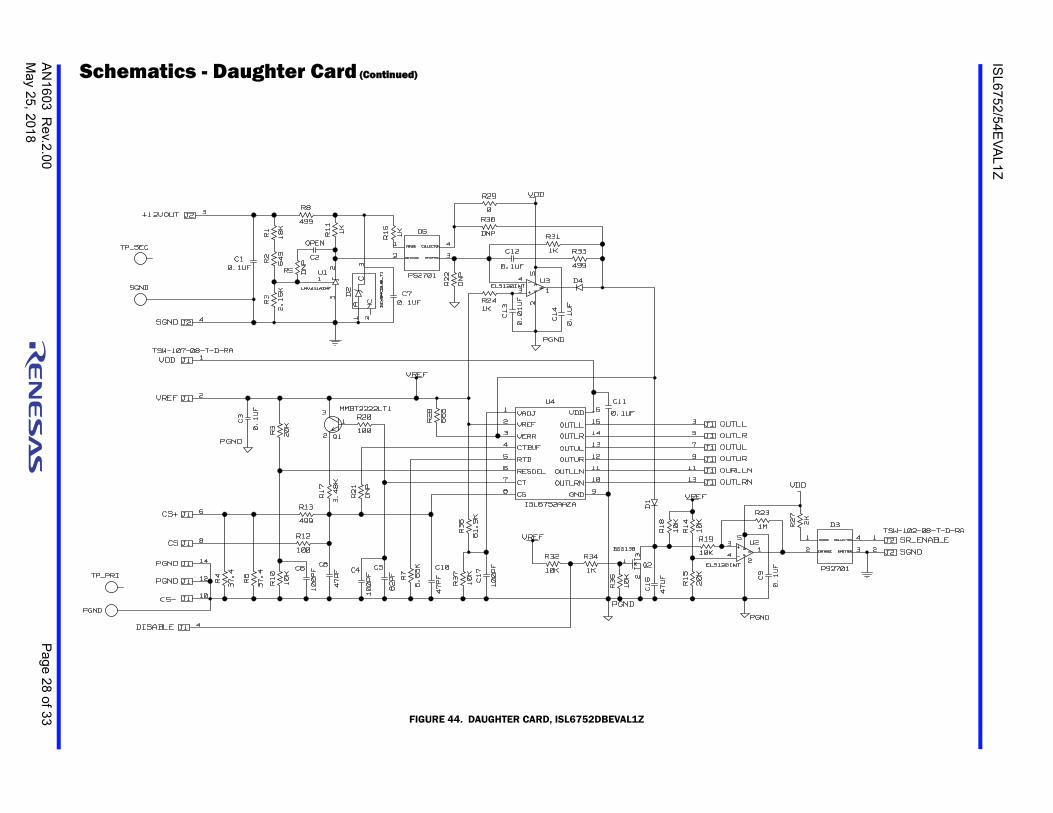
FIGURE 44. DAUGHTER CARD, ISL6752DBEVAL1Z
Schematics - Daughter Card (Continued)
CS-
R11
C11
3
U2
2.15
K
SGND
PGN
499
R8
ISL6752AAZA
61.9
K
MMBT2222LT1
D1
R2
665
R28
R37
10K
R36
R241K
PGND
C13
0.01
UF
0.1UF
C12
VDD
25
1
4
3EL5120IWT
U3
0.1U
F
C14
R31
1K
D4
R33
499
DNP
0
R29
C7D21 2
BZX8
4C6V
8LT1
3
J2 4
2
1
3
R5
LMV431AIMF
C10.1UF
OUTUR
OUTUL
J1
20.1UF
3
10K
5
4
1
PS2701
VREF
7
R15
20K
R20
R19
10KR32
20K
10K
R10 R7
6.65
K
PGND
R4 37.4 R6 37.4
R21
DNP
DNP
R17
3.48
K
R22
DNP
C2
18K
TP_SEC
TSW-107-08-T-D-RA
9
1K
R35
C16
47UF
2
VREF
U1
1K
4
3
J1
0.1U
F
1
7
8
VREF
SGND
J2 3
R3R1 1KR16 D5
1
2
VDD J1
VREF 2
DISABLE J1 4
C3
11J1
J1
C10
CS+
100P
F C5
PGND
J1 10
12J1
PGND 14J1
CS 8J1
J1 6R13
2
R18
10
R12
TP_PRI
PGND
11
16
6
12
13
14
15
9
U4
13 J1
J1
3
R9
C4C8
2
31
Q1
5
14
3
R341
Q2
C17C6
10047
PF
82PF
100P
F
47PF
OUTLL
100
499
100P
F
OUTLR
J15
PGND
OURLLN
OUTLRN
10K
10K
1
R30
0.1UF
OPEN
+12VOUT
BSS138
EL5120IWT
10K
R14
649
R2
COLLECTOR
EMITTERCATHODE
ANODE
VADJ
VREF
VERR
RTD
RESDEL
CT
CS GND
OUTLRN
OUTUR
OUTLR
OUTLL
VDD
OUTUL
OUTLLN
CTBUF
NCC
A
V+
V-
OUT
V+
V-
OUT
ISL6752/54EVAL1Z ZVS DC/DC Power Supply with
Synchronous Rectifiers Evaluation Board
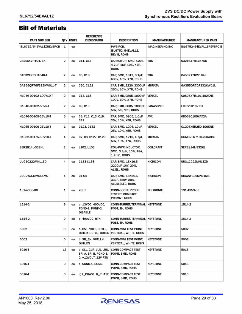
Bill of Materials
PART NUMBER QTY UNITSREFERENCE DESIGNATOR DESCRIPTION MANUFACTURER MANUFACTURER PART
ISL6752/54EVAL1ZREVBPCB 1 ea PWB-PCB, ISL6752_54EVAL1Z, REV B, ROHS
IMAGINEERING INC ISL6752/54EVAL1ZREVBPC B
C3216X7R1C475K-T 2 ea C11, C17 CAPACITOR, SMD, 1206, 4.7µF, 16V, 10%, X7R, ROHS
TDK C3216X7R1C475K
C4532X7R2J104K-T 2 ea C5, C18 CAP, SMD, 1812, 0.1µF, 630V, 10%, X7R, ROHS
TDK C4532X7R2J104K
GA355QR7GF332KW01L-T 2 ea C20, C121 CAP, SMD, 2220, 3300pF, 250V, 10%, X7R, ROHS
MURATA GA355QR7GF332KW01L
H1046-00102-100V10-T 2 ea C14, C15 CAP, SMD, 0805, 1000pF, 100V, 10%, X7R, ROHS
VENKEL C0805X7R101-102KNE
H1046-00102-50V5-T 2 ea C9, C10 CAP, SMD, 0805, 1000pF, 50V, 5%, NP0, ROHS
PANASONIC ECU-V1H102JCX
H1046-00105-25V10-T 5 ea C6, C12, C13, C16, C22
CAP, SMD, 0805, 1.0µF, 25V, 10%, X5R, ROHS
AVX 08053C105KAT2A
H1065-00106-25V10-T 1 ea C123, C132 CAP, SMD, 1206, 10µF, 25V, 10%, X5R, ROHS
VENKEL C1206X5R250-106KNE
H1082-00475-50V10-T 4 ea C7, C8, C127, C129 CAP, SMD, 1210, 4.7µF, 50V, 10%, X7R, ROHS
MURATA GRM32ER71H475KA88L
SER2814L-332KL 2 ea L102, L103 COIL-PWR INDUCTOR, SMD, 3.3µH, 10%, 48A, 1.2mΩ, ROHS
COILCRAFT SER2814L-332KL
UUG1C222MNL1ZD 4 ea C133-C136 CAP, SMD, 16X16.5, 2200µF, 16V, 20%, AL.EL., ROHS
NICHICON UUG1C222MNL1ZD
UUG2W330MNL1MS 4 ea C1-C4 CAP, SMD, 18X21.5, 33µF, 450V, 20%, ALUM.ELEC, ROHS
NICHICON UUG2W330MNL1MS
131-4353-00 1 ea VOUT CONN-SCOPE PROBE TEST PT, COMPACT, PCBMNT, ROHS
TEKTRONIX 131-4353-00
1514-2 6 ea a) 13VDC, 400VDC, PGND-1, PGND-2, DISABLE
CONN-TURRET, TERMINAL POST, TH, ROHS
KEYSTONE 1514-2
1514-2 0 ea b) 400VDC_RTN CONN-TURRET, TERMINAL POST, TH, ROHS
KEYSTONE 1514-2
5002 9 ea a) CS+, VREF, OUTLL, OUTLR, OUTUL, OUTUR
CONN-MINI TEST POINT, VERTICAL, WHITE, ROHS
KEYSTONE 5002
5002 0 ea b) SR_EN, OUTLLN, OUTLRN
CONN-MINI TEST POINT, VERTICAL, WHITE, ROHS
KEYSTONE 5002
5016-T 13 ea a) GLL, GLR, LLN, LRN, SR_A, SR_B, PGND-3, 2, +12VOUT, 12V RTN
CONN-COMPACT TEST POINT, SMD, ROHS
KEYSTONE 5016
5016-T 0 ea b) SGND-1, SGND- CONN-COMPACT TEST POINT, SMD, ROHS
KEYSTONE 5016
5016-T 0 ea c) L_PHASE, R_PHASE CONN-COMPACT TEST POINT, SMD, ROHS
KEYSTONE 5016
AN1603 Rev.2.00 Page 29 of 33May 25, 2018
ISL6752/54EVAL1Z ZVS DC/DC Power Supply with
Synchronous Rectifiers Evaluation Board
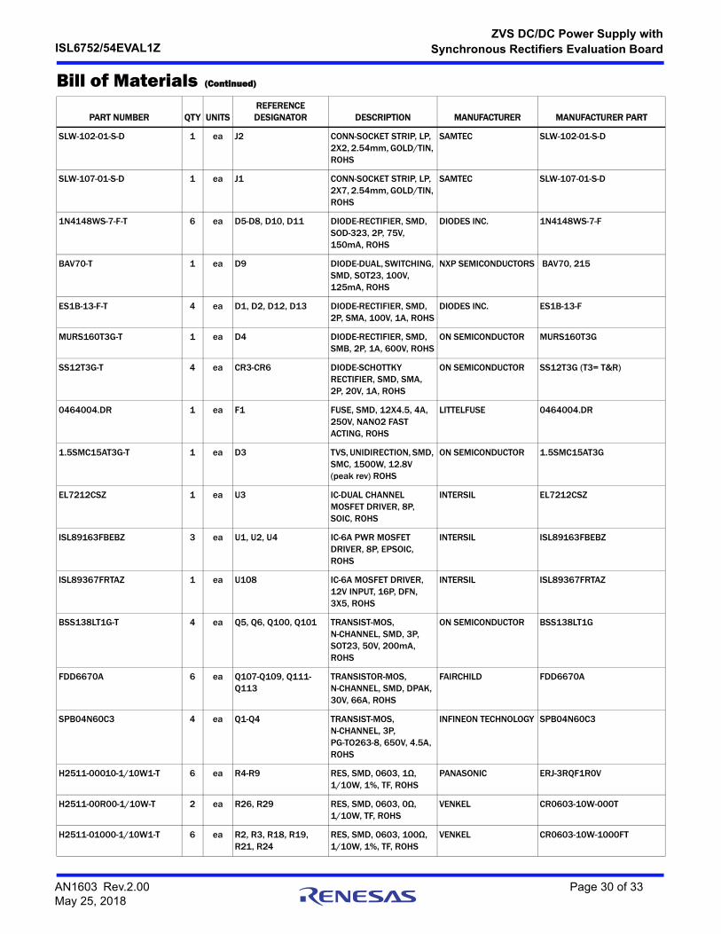
SLW-102-01-S-D 1 ea J2 CONN-SOCKET STRIP, LP, 2X2, 2.54mm, GOLD/TIN, ROHS
SAMTEC SLW-102-01-S-D
SLW-107-01-S-D 1 ea J1 CONN-SOCKET STRIP, LP, 2X7, 2.54mm, GOLD/TIN, ROHS
SAMTEC SLW-107-01-S-D
1N4148WS-7-F-T 6 ea D5-D8, D10, D11 DIODE-RECTIFIER, SMD, SOD-323, 2P, 75V, 150mA, ROHS
DIODES INC. 1N4148WS-7-F
BAV70-T 1 ea D9 DIODE-DUAL, SWITCHING, SMD, SOT23, 100V, 125mA, ROHS
NXP SEMICONDUCTORS BAV70, 215
ES1B-13-F-T 4 ea D1, D2, D12, D13 DIODE-RECTIFIER, SMD, 2P, SMA, 100V, 1A, ROHS
DIODES INC. ES1B-13-F
MURS160T3G-T 1 ea D4 DIODE-RECTIFIER, SMD, SMB, 2P, 1A, 600V, ROHS
ON SEMICONDUCTOR MURS160T3G
SS12T3G-T 4 ea CR3-CR6 DIODE-SCHOTTKY RECTIFIER, SMD, SMA, 2P, 20V, 1A, ROHS
ON SEMICONDUCTOR SS12T3G (T3= T&R)
0464004.DR 1 ea F1 FUSE, SMD, 12X4.5, 4A, 250V, NANO2 FAST ACTING, ROHS
LITTELFUSE 0464004.DR
1.5SMC15AT3G-T 1 ea D3 TVS, UNIDIRECTION, SMD, SMC, 1500W, 12.8V (peak rev) ROHS
ON SEMICONDUCTOR 1.5SMC15AT3G
EL7212CSZ 1 ea U3 IC-DUAL CHANNEL MOSFET DRIVER, 8P, SOIC, ROHS
INTERSIL EL7212CSZ
ISL89163FBEBZ 3 ea U1, U2, U4 IC-6A PWR MOSFET DRIVER, 8P, EPSOIC, ROHS
INTERSIL ISL89163FBEBZ
ISL89367FRTAZ 1 ea U108 IC-6A MOSFET DRIVER, 12V INPUT, 16P, DFN, 3X5, ROHS
INTERSIL ISL89367FRTAZ
BSS138LT1G-T 4 ea Q5, Q6, Q100, Q101 TRANSIST-MOS, N-CHANNEL, SMD, 3P, SOT23, 50V, 200mA, ROHS
ON SEMICONDUCTOR BSS138LT1G
FDD6670A 6 ea Q107-Q109, Q111-Q113
TRANSISTOR-MOS, N-CHANNEL, SMD, DPAK, 30V, 66A, ROHS
FAIRCHILD FDD6670A
SPB04N60C3 4 ea Q1-Q4 TRANSIST-MOS, N-CHANNEL, 3P, PG-TO263-8, 650V, 4.5A, ROHS
INFINEON TECHNOLOGY SPB04N60C3
H2511-00010-1/10W1-T 6 ea R4-R9 RES, SMD, 0603, 1Ω, 1/10W, 1%, TF, ROHS
PANASONIC ERJ-3RQF1R0V
H2511-00R00-1/10W-T 2 ea R26, R29 RES, SMD, 0603, 0Ω, 1/10W, TF, ROHS
VENKEL CR0603-10W-000T
H2511-01000-1/10W1-T 6 ea R2, R3, R18, R19, R21, R24
RES, SMD, 0603, 100Ω, 1/10W, 1%, TF, ROHS
VENKEL CR0603-10W-1000FT
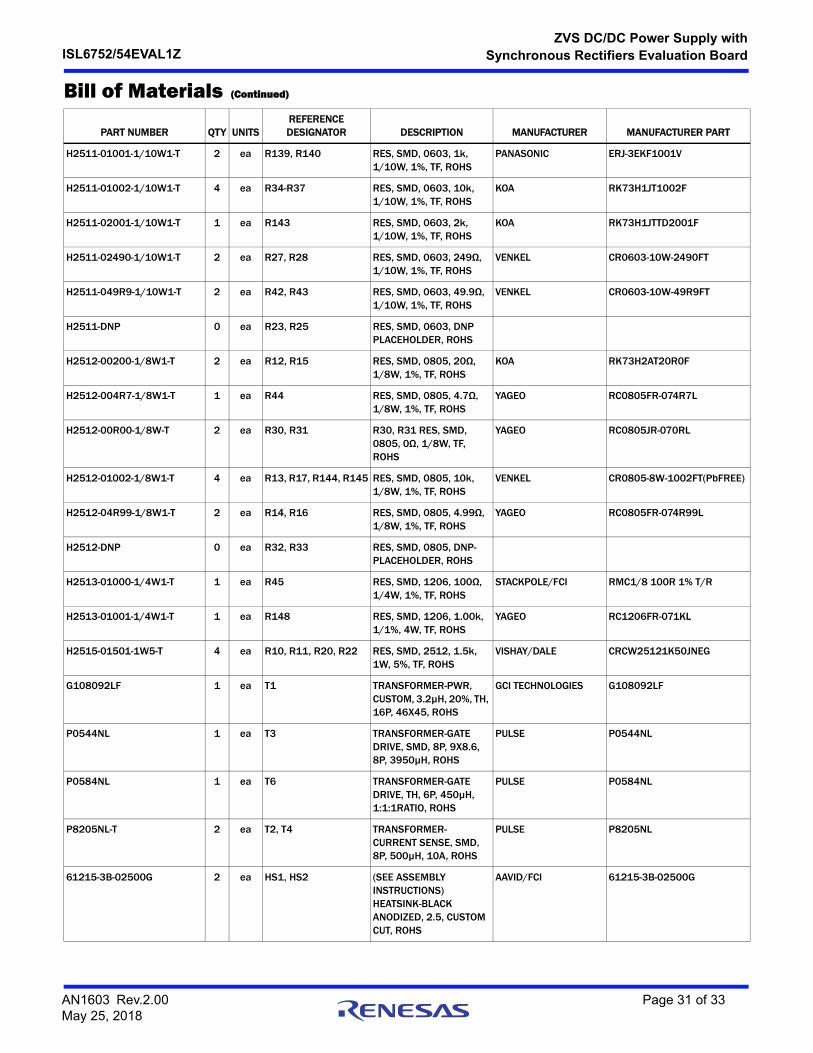
Bill of Materials (Continued)
PART NUMBER QTY UNITSREFERENCE DESIGNATOR DESCRIPTION MANUFACTURER MANUFACTURER PART
AN1603 Rev.2.00 Page 30 of 33May 25, 2018
ISL6752/54EVAL1Z ZVS DC/DC Power Supply with
Synchronous Rectifiers Evaluation Board
H2511-01001-1/10W1-T 2 ea R139, R140 RES, SMD, 0603, 1k, 1/10W, 1%, TF, ROHS
PANASONIC ERJ-3EKF1001V
H2511-01002-1/10W1-T 4 ea R34-R37 RES, SMD, 0603, 10k, 1/10W, 1%, TF, ROHS
KOA RK73H1JT1002F
H2511-02001-1/10W1-T 1 ea R143 RES, SMD, 0603, 2k, 1/10W, 1%, TF, ROHS
KOA RK73H1JTTD2001F
H2511-02490-1/10W1-T 2 ea R27, R28 RES, SMD, 0603, 249Ω, 1/10W, 1%, TF, ROHS
VENKEL CR0603-10W-2490FT
H2511-049R9-1/10W1-T 2 ea R42, R43 RES, SMD, 0603, 49.9Ω, 1/10W, 1%, TF, ROHS
VENKEL CR0603-10W-49R9FT
H2511-DNP 0 ea R23, R25 RES, SMD, 0603, DNP PLACEHOLDER, ROHS
H2512-00200-1/8W1-T 2 ea R12, R15 RES, SMD, 0805, 20Ω, 1/8W, 1%, TF, ROHS
KOA RK73H2AT20R0F
H2512-004R7-1/8W1-T 1 ea R44 RES, SMD, 0805, 4.7Ω, 1/8W, 1%, TF, ROHS
YAGEO RC0805FR-074R7L
H2512-00R00-1/8W-T 2 ea R30, R31 R30, R31 RES, SMD, 0805, 0Ω, 1/8W, TF, ROHS
YAGEO RC0805JR-070RL
H2512-01002-1/8W1-T 4 ea R13, R17, R144, R145 RES, SMD, 0805, 10k, 1/8W, 1%, TF, ROHS
VENKEL CR0805-8W-1002FT(PbFREE)
H2512-04R99-1/8W1-T 2 ea R14, R16 RES, SMD, 0805, 4.99Ω, 1/8W, 1%, TF, ROHS
YAGEO RC0805FR-074R99L
H2512-DNP 0 ea R32, R33 RES, SMD, 0805, DNP-PLACEHOLDER, ROHS
H2513-01000-1/4W1-T 1 ea R45 RES, SMD, 1206, 100Ω, 1/4W, 1%, TF, ROHS
STACKPOLE/FCI RMC1/8 100R 1% T/R
H2513-01001-1/4W1-T 1 ea R148 RES, SMD, 1206, 1.00k, 1/1%, 4W, TF, ROHS
YAGEO RC1206FR-071KL
H2515-01501-1W5-T 4 ea R10, R11, R20, R22 RES, SMD, 2512, 1.5k, 1W, 5%, TF, ROHS
VISHAY/DALE CRCW25121K50JNEG
G108092LF 1 ea T1 TRANSFORMER-PWR, CUSTOM, 3.2µH, 20%, TH, 16P, 46X45, ROHS
GCI TECHNOLOGIES G108092LF
P0544NL 1 ea T3 TRANSFORMER-GATE DRIVE, SMD, 8P, 9X8.6, 8P, 3950µH, ROHS
PULSE P0544NL
P0584NL 1 ea T6 TRANSFORMER-GATE DRIVE, TH, 6P, 450µH, 1:1:1RATIO, ROHS
PULSE P0584NL
P8205NL-T 2 ea T2, T4 TRANSFORMER-CURRENT SENSE, SMD, 8P, 500µH, 10A, ROHS
PULSE P8205NL
61215-3B-02500G 2 ea HS1, HS2 (SEE ASSEMBLY INSTRUCTIONS) HEATSINK-BLACK ANODIZED, 2.5, CUSTOM CUT, ROHS
AAVID/FCI 61215-3B-02500G
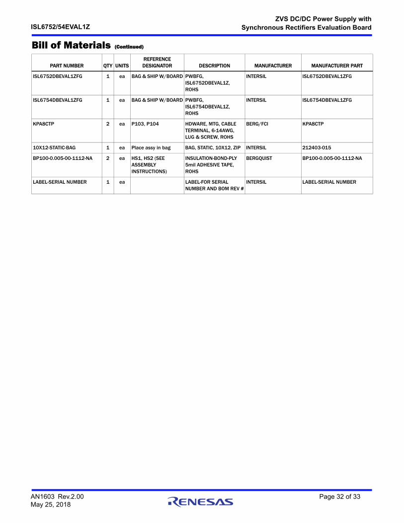
Bill of Materials (Continued)
PART NUMBER QTY UNITSREFERENCE DESIGNATOR DESCRIPTION MANUFACTURER MANUFACTURER PART
AN1603 Rev.2.00 Page 31 of 33May 25, 2018
ISL6752/54EVAL1Z ZVS DC/DC Power Supply with
Synchronous Rectifiers Evaluation Board
ISL6752DBEVAL1ZFG 1 ea BAG & SHIP W/BOARD PWBFG, ISL6752DBEVAL1Z, ROHS
INTERSIL ISL6752DBEVAL1ZFG
ISL6754DBEVAL1ZFG 1 ea BAG & SHIP W/BOARD PWBFG, ISL6754DBEVAL1Z, ROHS
INTERSIL ISL6754DBEVAL1ZFG
KPA8CTP 2 ea P103, P104 HDWARE, MTG, CABLE TERMINAL, 6-14AWG, LUG & SCREW, ROHS
BERG/FCI KPA8CTP
10X12-STATIC-BAG 1 ea Place assy in bag BAG, STATIC, 10X12, ZIP INTERSIL 212403-015
BP100-0.005-00-1112-NA 2 ea HS1, HS2 (SEE ASSEMBLY INSTRUCTIONS)
INSULATION-BOND-PLY 5mil ADHESIVE TAPE, ROHS
BERGQUIST BP100-0.005-00-1112-NA
LABEL-SERIAL NUMBER 1 ea LABEL-FOR SERIAL NUMBER AND BOM REV #
INTERSIL LABEL-SERIAL NUMBER
Bill of Materials (Continued)
PART NUMBER QTY UNITSREFERENCE DESIGNATOR DESCRIPTION MANUFACTURER MANUFACTURER PART
AN1603 Rev.2.00 Page 32 of 33May 25, 2018
http://www.renesas.comRefer to "http://www.renesas.com/" for the latest and detailed information.
Renesas Electronics America Inc.1001 Murphy Ranch Road, Milpitas, CA 95035, U.S.A.Tel: +1-408-432-8888, Fax: +1-408-434-5351Renesas Electronics Canada Limited9251 Yonge Street, Suite 8309 Richmond Hill, Ontario Canada L4C 9T3Tel: +1-905-237-2004Renesas Electronics Europe LimitedDukes Meadow, Millboard Road, Bourne End, Buckinghamshire, SL8 5FH, U.KTel: +44-1628-651-700, Fax: +44-1628-651-804Renesas Electronics Europe GmbHArcadiastrasse 10, 40472 Düsseldorf, Germany Tel: +49-211-6503-0, Fax: +49-211-6503-1327Renesas Electronics (China) Co., Ltd.Room 1709 Quantum Plaza, No.27 ZhichunLu, Haidian District, Beijing, 100191 P. R. ChinaTel: +86-10-8235-1155, Fax: +86-10-8235-7679Renesas Electronics (Shanghai) Co., Ltd.Unit 301, Tower A, Central Towers, 555 Langao Road, Putuo District, Shanghai, 200333 P. R. China Tel: +86-21-2226-0888, Fax: +86-21-2226-0999Renesas Electronics Hong Kong LimitedUnit 1601-1611, 16/F., Tower 2, Grand Century Place, 193 Prince Edward Road West, Mongkok, Kowloon, Hong KongTel: +852-2265-6688, Fax: +852 2886-9022Renesas Electronics Taiwan Co., Ltd.13F, No. 363, Fu Shing North Road, Taipei 10543, TaiwanTel: +886-2-8175-9600, Fax: +886 2-8175-9670Renesas Electronics Singapore Pte. Ltd.80 Bendemeer Road, Unit #06-02 Hyflux Innovation Centre, Singapore 339949Tel: +65-6213-0200, Fax: +65-6213-0300Renesas Electronics Malaysia Sdn.Bhd.Unit 1207, Block B, Menara Amcorp, Amcorp Trade Centre, No. 18, Jln Persiaran Barat, 46050 Petaling Jaya, Selangor Darul Ehsan, MalaysiaTel: +60-3-7955-9390, Fax: +60-3-7955-9510Renesas Electronics India Pvt. Ltd.No.777C, 100 Feet Road, HAL 2nd Stage, Indiranagar, Bangalore 560 038, IndiaTel: +91-80-67208700, Fax: +91-80-67208777Renesas Electronics Korea Co., Ltd.17F, KAMCO Yangjae Tower, 262, Gangnam-daero, Gangnam-gu, Seoul, 06265 KoreaTel: +82-2-558-3737, Fax: +82-2-558-5338
SALES OFFICES
© 2018 Renesas Electronics Corporation. All rights reserved.Colophon 7.0
(Rev.4.0-1 November 2017)
Notice
1. Descriptions of circuits, software and other related information in this document are provided only to illustrate the operation of semiconductor products and application examples. You are fully responsible for
the incorporation or any other use of the circuits, software, and information in the design of your product or system. Renesas Electronics disclaims any and all liability for any losses and damages incurred by
you or third parties arising from the use of these circuits, software, or information.
2. Renesas Electronics hereby expressly disclaims any warranties against and liability for infringement or any other claims involving patents, copyrights, or other intellectual property rights of third parties, by or
arising from the use of Renesas Electronics products or technical information described in this document, including but not limited to, the product data, drawings, charts, programs, algorithms, and application
examples.
3. No license, express, implied or otherwise, is granted hereby under any patents, copyrights or other intellectual property rights of Renesas Electronics or others.
4. You shall not alter, modify, copy, or reverse engineer any Renesas Electronics product, whether in whole or in part. Renesas Electronics disclaims any and all liability for any losses or damages incurred by
you or third parties arising from such alteration, modification, copying or reverse engineering.
5. Renesas Electronics products are classified according to the following two quality grades: “Standard” and “High Quality”. The intended applications for each Renesas Electronics product depends on the
product’s quality grade, as indicated below.
"Standard": Computers; office equipment; communications equipment; test and measurement equipment; audio and visual equipment; home electronic appliances; machine tools; personal electronic
equipment; industrial robots; etc.
"High Quality": Transportation equipment (automobiles, trains, ships, etc.); traffic control (traffic lights); large-scale communication equipment; key financial terminal systems; safety control equipment; etc.
Unless expressly designated as a high reliability product or a product for harsh environments in a Renesas Electronics data sheet or other Renesas Electronics document, Renesas Electronics products are
not intended or authorized for use in products or systems that may pose a direct threat to human life or bodily injury (artificial life support devices or systems; surgical implantations; etc.), or may cause
serious property damage (space system; undersea repeaters; nuclear power control systems; aircraft control systems; key plant systems; military equipment; etc.). Renesas Electronics disclaims any and all
liability for any damages or losses incurred by you or any third parties arising from the use of any Renesas Electronics product that is inconsistent with any Renesas Electronics data sheet, user’s manual or
other Renesas Electronics document.
6. When using Renesas Electronics products, refer to the latest product information (data sheets, user’s manuals, application notes, “General Notes for Handling and Using Semiconductor Devices” in the
reliability handbook, etc.), and ensure that usage conditions are within the ranges specified by Renesas Electronics with respect to maximum ratings, operating power supply voltage range, heat dissipation
characteristics, installation, etc. Renesas Electronics disclaims any and all liability for any malfunctions, failure or accident arising out of the use of Renesas Electronics products outside of such specified
ranges.
7. Although Renesas Electronics endeavors to improve the quality and reliability of Renesas Electronics products, semiconductor products have specific characteristics, such as the occurrence of failure at a
certain rate and malfunctions under certain use conditions. Unless designated as a high reliability product or a product for harsh environments in a Renesas Electronics data sheet or other Renesas
Electronics document, Renesas Electronics products are not subject to radiation resistance design. You are responsible for implementing safety measures to guard against the possibility of bodily injury, injury
or damage caused by fire, and/or danger to the public in the event of a failure or malfunction of Renesas Electronics products, such as safety design for hardware and software, including but not limited to
redundancy, fire control and malfunction prevention, appropriate treatment for aging degradation or any other appropriate measures. Because the evaluation of microcomputer software alone is very difficult
and impractical, you are responsible for evaluating the safety of the final products or systems manufactured by you.
8. Please contact a Renesas Electronics sales office for details as to environmental matters such as the environmental compatibility of each Renesas Electronics product. You are responsible for carefully and
sufficiently investigating applicable laws and regulations that regulate the inclusion or use of controlled substances, including without limitation, the EU RoHS Directive, and using Renesas Electronics
products in compliance with all these applicable laws and regulations. Renesas Electronics disclaims any and all liability for damages or losses occurring as a result of your noncompliance with applicable
laws and regulations.
9. Renesas Electronics products and technologies shall not be used for or incorporated into any products or systems whose manufacture, use, or sale is prohibited under any applicable domestic or foreign laws
or regulations. You shall comply with any applicable export control laws and regulations promulgated and administered by the governments of any countries asserting jurisdiction over the parties or
transactions.
10. It is the responsibility of the buyer or distributor of Renesas Electronics products, or any other party who distributes, disposes of, or otherwise sells or transfers the product to a third party, to notify such third
party in advance of the contents and conditions set forth in this document.
11. This document shall not be reprinted, reproduced or duplicated in any form, in whole or in part, without prior written consent of Renesas Electronics.
12. Please contact a Renesas Electronics sales office if you have any questions regarding the information contained in this document or Renesas Electronics products.
(Note 1) “Renesas Electronics” as used in this document means Renesas Electronics Corporation and also includes its directly or indirectly controlled subsidiaries.
(Note 2) “Renesas Electronics product(s)” means any product developed or manufactured by or for Renesas Electronics.


![SAP HowTo Guide - Unlocking User SAPStar [User Guide]](https://img.pdfslide.us/doc/110x75/544ac849b1af9f7c4f8b4bd1/sap-howto-guide-unlocking-user-sapstar-user-guide.jpg)


![User Guide...User. {{]}]} {}]}](https://img.pdfslide.us/doc/110x75/60918ca14327954d24291644/-user-guide-user-.jpg)