Embed Size (px)
Citation preview
S32K1xx Firmware updates
by: NXP Semiconductors
1 Introduction
With the current technological advances, the vehicles are
becoming more electronical than mechanical. The
electronic innovation in vehicles is constantly increasing.
Consequently, the software in the vehicles is also
increasing and hence the risk of a potential bug.
Each time a software bug is found a recall process is
necessary to update the software. These recalls represent a
cost into the car manufacturers and also a time consuming
procedure for the final users.
Nowadays over the air updates start to be implemented on
the new vehicles using a/b swap technique. The updates
done using this technique are limited only to
microcontroller with high density memory, such as the
gateway or infotainment unit. Smaller microcontroller used
for edge node applications does not get updated.
In addition of taking care of the firmware update on the
edge node microcontrollers, another concern is to keep the
update process secure. This in order to protect the update
against possible eavesdropping, replication attacks.
This application note is focused on showing how the
S32K1xx microcontrollers handles the a/b swap updates
using a secure communication process. It explains the basic
concepts of a bootloader, a/b swap updates, and security
concepts. This document covers the implementation of
firmware updates as a whole system. For the functional
details of specific modules such as the flash controller, the
security module, CAN controller, etc. Please refer to the
S32K1xx devices reference manual.
NXP Semiconductors Document Number: AN12323
Application Notes Rev. 0 , 12/2018
Contents
1 Introduction ........................................................................ 1 2 Bootloader Concepts .......................................................... 2 3 Firmware update methods .................................................. 5 4 Security Concepts ............................................................... 6 5 S32K1xx Overview ............................................................ 8
5.1 NVM Architecture ................................................. 10 6 S321xx Firmware update implementations ...................... 11
6.1 S32K144 use case .................................................. 11 6.2 S32K146 use case .................................................. 16 6.3 A/B Swap using Position Independent Code (PIC) 25 6.4 Communication process ........................................ 26 6.5 Secure Communication ......................................... 27 6.6 Use Cases Implementation .................................... 28
7 Demo ................................................................................ 33 7.1 Setting up the demo ............................................... 36
8 References ........................................................................ 42
by: NXP Semiconductors, Application Notes, Rev. 0, 12/2018
NXP Semiconductors 2
Complementary software is included with this application note to demonstrate a/b swap updates while
leveraging the capabilities of S32K144 and S32K146 microcontrollers.
2 Bootloader concepts
During an application’s firmware development phase, updates to the microcontroller are done using a
flash programming tool which requires a certain number of microcontroller’s I/O’s and a special header
to interact with this tool. Once firmware is finalized, it is downloaded to the microcontroller which is
soldered in the final pcb. This pcb may or not include the required header for the programming tool, to
avoid access to data stored in flash or because application requires the I/O’s for its application. In some
cases, the final module hosting the microcontroller is in a difficult position to access, such as in the
automotive application in where electronic control units are placed in areas hidden for the final user. So,
what if an update to the firmware is required after the device is in the field, due to a failure or an
upgrade? To solve this problem bootloaders are developed.
A bootloader is a piece of firmware that resides in microcontroller’s Nonvolatile Memory (NVM), that
handles the updates of the application program or data. Bootloader and application might reside in the
same nonvolatile memory block, or in separate blocks. Application firmware and bootloader should not
be overlapped in the memory; hence bootloader is typically placed at start of the memory space. The
bootloader is not expected to be updated, hence the area in where it is located is protected to avoid
intentional or unintentional modifications.
The bootloader receives new firmware data from a host via a communication protocol, including but not
limited to CAN, LIN, UART, ETHERNET and USB. This communication protocol depends on the
developer’s decision, application and microcontroller features. The host sends the new firmware using a
known format, for instance srec or a bin file. The bootloader captures the packets with the new firmware
data to then update the memory locations where the old firmware is placed. Once the complete firmware
has been received and validated, the bootloader will jump to the new application.
Before getting into the details of the bootloader update algorithm, it’s necessary to understand the write
process into a NVM. To write into a NVM location, the data must be erased first, erase of data in
nonvolatile memories is done by sectors. This sector size is the smallest portion of data that can be
erased, it depends on each nonvolatile memory technology and it is known as the granularity of the
memory. Once the sector has been erased, data can be written into that sector. The write process also
depends on the NVM technology, each NVM has a number of bytes that can be written per write
command. Lastly, to complete the write process a program check command is necessary to verify that
data was written in flash as expected, this program check is done by write command.
Bootloader firmware size depends on the nonvolatile memory granularity. The bigger the granularity,
smaller sectors size, more flexibility is available for the size of the bootloader. Since the bootloader will
be receiving new firmware data from the host that will be programmed into the NVM, its necessary to
consider that the sector is previously erased before writing data to it.
During the update process, bootloader firmware which is read and executed from NVM, launches erase
and write commands to update the new application data into the NVM itself, therefore simultaneous
operations within the memory must be considered. Memory allowed simultaneous operations are
specific on each device, some devices allow to read while write into the memory as long as this occurs
in different read partitions or memory blocks. In case write while reading feature is not available,
Bootloader concepts
by: NXP Semiconductors, Application Notes, Rev. 0, 12/2018
NXP Semiconductors 3
bootloader needs to place the memory commands into ram location so these can be launched from there
to avoid any collisions.
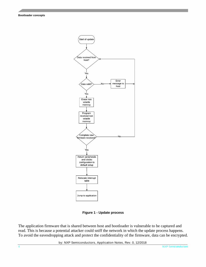
Entering to the update process can be done following a software or hardware approach. The triggers to
the update with the press of a button during a certain amount of time, state of an input low or high after
reset, or by receiving a specific communication packet that indicates an update is necessary while the
application is running. Typically, after a microcontroller reset, bootloader firmware checks during a
certain amount of time whether there is a condition to start the update process, in case this condition is
not met it then jumps to the application firmware. Some use cases can also check this trigger while the
application is running, allowing to do an update while running and avoid the downtime after a reset, so
in the next reset the device immediately boots to newest image. The decision on how the update process
is trigger, depends on the final application, memory and device features.
When the update process trigger is detected, the update algorithm starts to place the new firmware
application into the NVM. The update algorithm consists in the following steps: receive data from
communication protocol, validate that data received is correct, erase/program flash, check if the
complete data has been downloaded.
After the update process, bootloader should return the used peripherals and clock configurations to the
default state. This is necessary if bootloader starts after reset. Beside the peripherals and clock
configurations, the interrupt vector table should be relocated. The application firmware may use an
interrupt table in a different location, if this is the case the pointer to the interrupt table must be relocated
from its default position. Once these considerations are handled, bootloader can then jump to the
application firmware. A flow diagram of the update process is shown in the figure below.
Bootloader concepts
by: NXP Semiconductors, Application Notes, Rev. 0, 12/2018
4 NXP Semiconductors
The application firmware that is shared between host and bootloader is vulnerable to be captured and
read. This is because a potential attacker could sniff the network in which the update process happens.
To avoid the eavesdropping attack and protect the confidentiality of the firmware, data can be encrypted.
Figure 1 - Update process
Firmware update methods
by: NXP Semiconductors, Application Notes, Rev. 0, 12/2018
NXP Semiconductors 5
Encryption of the data can happen in the host before it is transmitted in the network. Then, bootloader
needs to decrypt this data using a known key before writing it to NVM memory. Besides the encryption,
mechanisms to validate the host authenticity and the freshness of the data can be added into the
bootloader.
Finally, when developing the bootloader firmware, location in memory should be considered.
Bootloader firmware and application might reside in the same NVM memory block, hence it is
necessary to modify bootloader and application firmware linker files to avoid overlaps. There are some
devices that have a dedicated location in memory to place the bootloader. Linker file modification
depends on the microcontroller and compiler that is used.
3 Firmware update methods
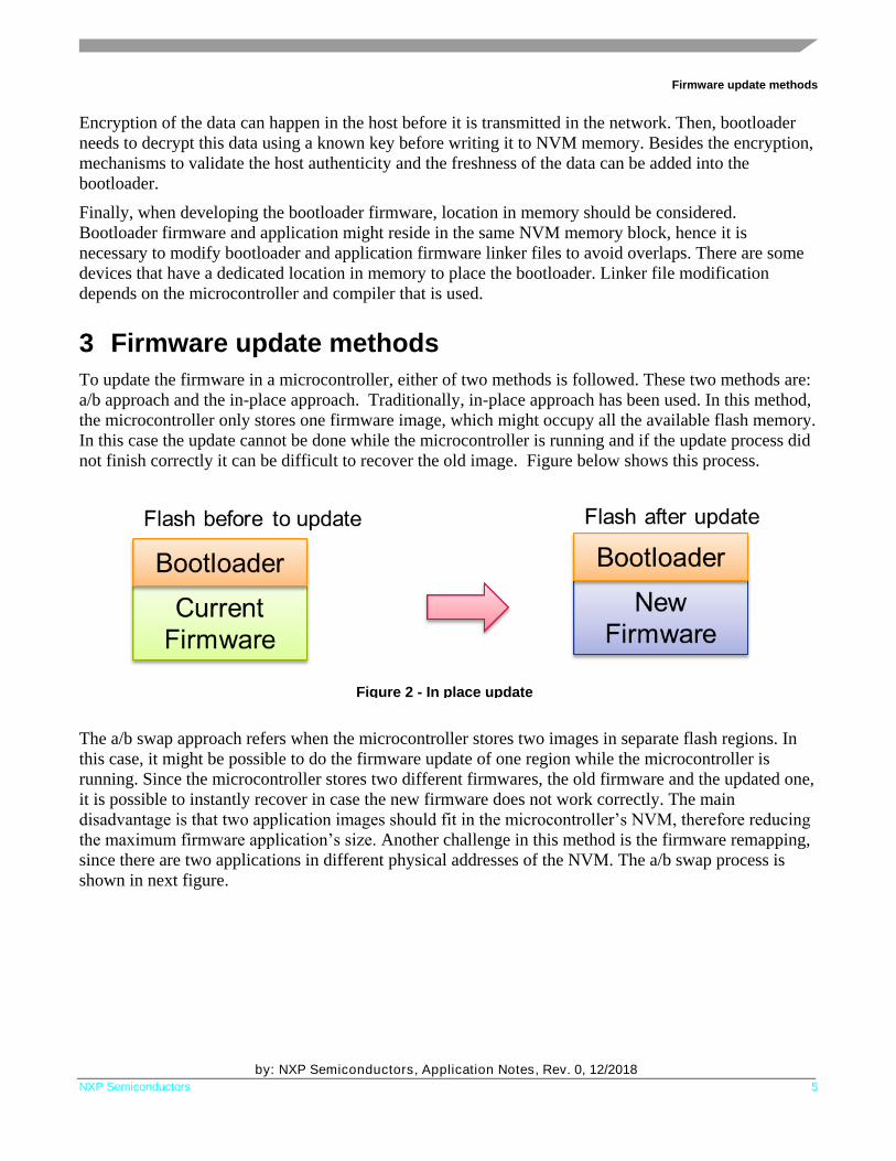
To update the firmware in a microcontroller, either of two methods is followed. These two methods are:
a/b approach and the in-place approach. Traditionally, in-place approach has been used. In this method,
the microcontroller only stores one firmware image, which might occupy all the available flash memory.
In this case the update cannot be done while the microcontroller is running and if the update process did
not finish correctly it can be difficult to recover the old image. Figure below shows this process.
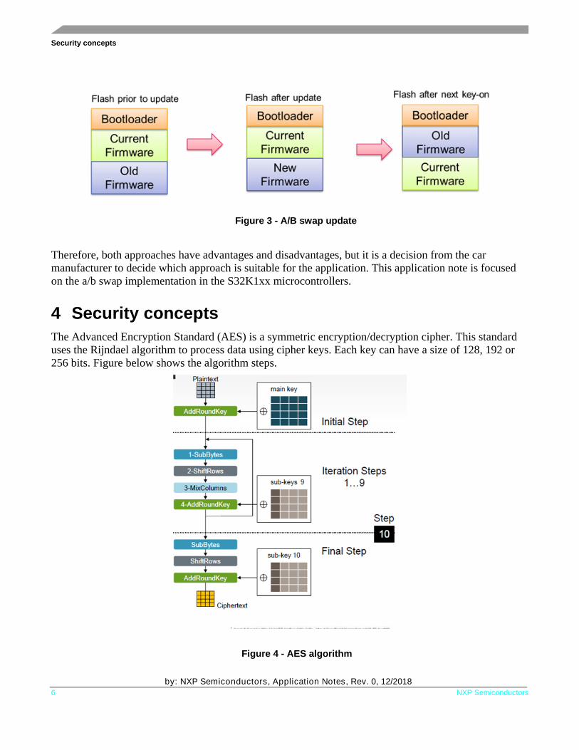
The a/b swap approach refers when the microcontroller stores two images in separate flash regions. In
this case, it might be possible to do the firmware update of one region while the microcontroller is
running. Since the microcontroller stores two different firmwares, the old firmware and the updated one,
it is possible to instantly recover in case the new firmware does not work correctly. The main
disadvantage is that two application images should fit in the microcontroller’s NVM, therefore reducing
the maximum firmware application’s size. Another challenge in this method is the firmware remapping,
since there are two applications in different physical addresses of the NVM. The a/b swap process is
shown in next figure.
Figure 2 - In place update
Security concepts
by: NXP Semiconductors, Application Notes, Rev. 0, 12/2018
6 NXP Semiconductors
Therefore, both approaches have advantages and disadvantages, but it is a decision from the car
manufacturer to decide which approach is suitable for the application. This application note is focused
on the a/b swap implementation in the S32K1xx microcontrollers.
4 Security concepts
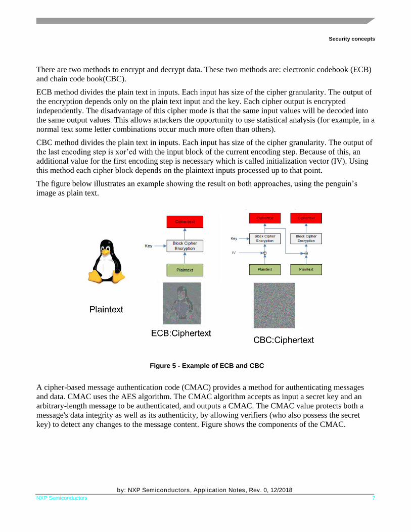
The Advanced Encryption Standard (AES) is a symmetric encryption/decryption cipher. This standard
uses the Rijndael algorithm to process data using cipher keys. Each key can have a size of 128, 192 or
256 bits. Figure below shows the algorithm steps.
Figure 3 - A/B swap update
Figure 4 - AES algorithm
Security concepts
by: NXP Semiconductors, Application Notes, Rev. 0, 12/2018
NXP Semiconductors 7
There are two methods to encrypt and decrypt data. These two methods are: electronic codebook (ECB)
and chain code book(CBC).
ECB method divides the plain text in inputs. Each input has size of the cipher granularity. The output of
the encryption depends only on the plain text input and the key. Each cipher output is encrypted
independently. The disadvantage of this cipher mode is that the same input values will be decoded into
the same output values. This allows attackers the opportunity to use statistical analysis (for example, in a
normal text some letter combinations occur much more often than others).
CBC method divides the plain text in inputs. Each input has size of the cipher granularity. The output of
the last encoding step is xor’ed with the input block of the current encoding step. Because of this, an
additional value for the first encoding step is necessary which is called initialization vector (IV). Using
this method each cipher block depends on the plaintext inputs processed up to that point.
The figure below illustrates an example showing the result on both approaches, using the penguin’s
image as plain text.
A cipher-based message authentication code (CMAC) provides a method for authenticating messages
and data. CMAC uses the AES algorithm. The CMAC algorithm accepts as input a secret key and an
arbitrary-length message to be authenticated, and outputs a CMAC. The CMAC value protects both a
message's data integrity as well as its authenticity, by allowing verifiers (who also possess the secret
key) to detect any changes to the message content. Figure shows the components of the CMAC.
Figure 5 - Example of ECB and CBC
S32K1xx overview
by: NXP Semiconductors, Application Notes, Rev. 0, 12/2018
8 NXP Semiconductors
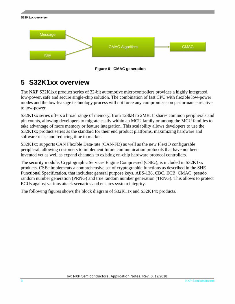
5 S32K1xx overview
The NXP S32K1xx product series of 32-bit automotive microcontrollers provides a highly integrated,
low-power, safe and secure single-chip solution. The combination of fast CPU with flexible low-power
modes and the low-leakage technology process will not force any compromises on performance relative
to low-power.
S32K1xx series offers a broad range of memory, from 128kB to 2MB. It shares common peripherals and
pin counts, allowing developers to migrate easily within an MCU family or among the MCU families to
take advantage of more memory or feature integration. This scalability allows developers to use the
S32K1xx product series as the standard for their end product platforms, maximizing hardware and
software reuse and reducing time to market.
S32K1xx supports CAN Flexible Data-rate (CAN-FD) as well as the new FlexIO configurable
peripheral, allowing customers to implement future communication protocols that have not been
invented yet as well as expand channels to existing on-chip hardware protocol controllers.
The security module, Cryptographic Services Engine Compressed (CSEc), is included in S32K1xx
products. CSEc implements a comprehensive set of cryptographic functions as described in the SHE
Functional Specification, that includes: general purpose keys, AES-128, CBC, ECB, CMAC, pseudo
random number generation (PRNG) and true random number generation (TRNG). This allows to protect
ECUs against various attack scenarios and ensures system integrity.
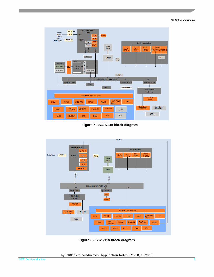
The following figures shows the block diagram of S32K11x and S32K14x products.
Figure 6 - CMAC generation
S32K1xx overview
by: NXP Semiconductors, Application Notes, Rev. 0, 12/2018
NXP Semiconductors 9
Figure 7 - S32K14x block diagram
Figure 8 - S32K11x block diagram

S32K1xx overview
by: NXP Semiconductors, Application Notes, Rev. 0, 12/2018
10 NXP Semiconductors
5.1 NVM architecture
S32K1xx microcontrollers have a C90TFS (thin film storage) technology flash. There are two flash
memories in these devices, the program flash (pflash) and the flex memory.
Program flash is a nonvolatile memory whose main purpose is to execute code. The size of the program
flash varies from device to device and it is in the range of 128kB to 1.5 MB. This flash features a sector
size of 4kB in devices with a program flash higher than 256kB and of 2kB for devices with a program
flash equal or less to 256kB. In all the devices, the pflash programming command writes 8B at a time.
The block size of this flash is of 512kB or less, depending on the device there are one or more flash
blocks. Each block represents a read partition, this means that a block can be read while another is being
erased or written.
Flex memory flash purpose is to execute code, store data or function as EEPROM in conjunction with
the flex ram memory. Size of this flex memory varies in each device, 32kB (S32K11x), 64kB
(S32K142/4/6) or 512kB (S32K148). The size of the sector in this memory is of 2kB for S32K116/8 and
S32K142/4/6 devices, while for the S32K148 device the sector size is of 4kB. In all the devices, the flex
memory programming command writes 8B at a time. The flex memory is a separate read partition,
therefore reading from this flash can be done while erasing or writing program flash, and vice versa. In
case the flex memory is configured to function as EEPROM, it can be partitioned so that part of the flex
memory stores code or data, while the other part is used as EEPROM backup. The sizes that flex
memory can be divided into are: 16kB, 32kB and 64kB.
A summary of the sizes and flash granularity for each S32K1xx device is shown in the below table. The
location of these memories in the memory map for each device is shown in figure 9.
Table 1 S32K1xx memory sizes
Device Program Flash Program Flash
sector size
Flex memory Flex memory
sector size
S32K116 128kB 2kB 32kB 2kB
S32K118 256kB 2kB 32kB 2kB
S32K142 256kB 2kB 64kB 2kB
S32K144 512kB 4kB 64kB 2kB
S32K146 1 MB 4kB 64kB 2kB
S32K148 1.5 MB 4kB 512kB 4kB

S321xx Firmware update implementations
by: NXP Semiconductors, Application Notes, Rev. 0, 12/2018
NXP Semiconductors 11
A flash controller is included within the microcontroller for these memories. This flash controller
executes the commands to erase, program and check these memories. Besides the commands to access
the content in these memories, also security commands are included. Commands such as encryption,
decryption, cmac calculations, random number generations can be executed from the flash controller.
6 S321xx Firmware update implementations
6.1 S32K144 use case
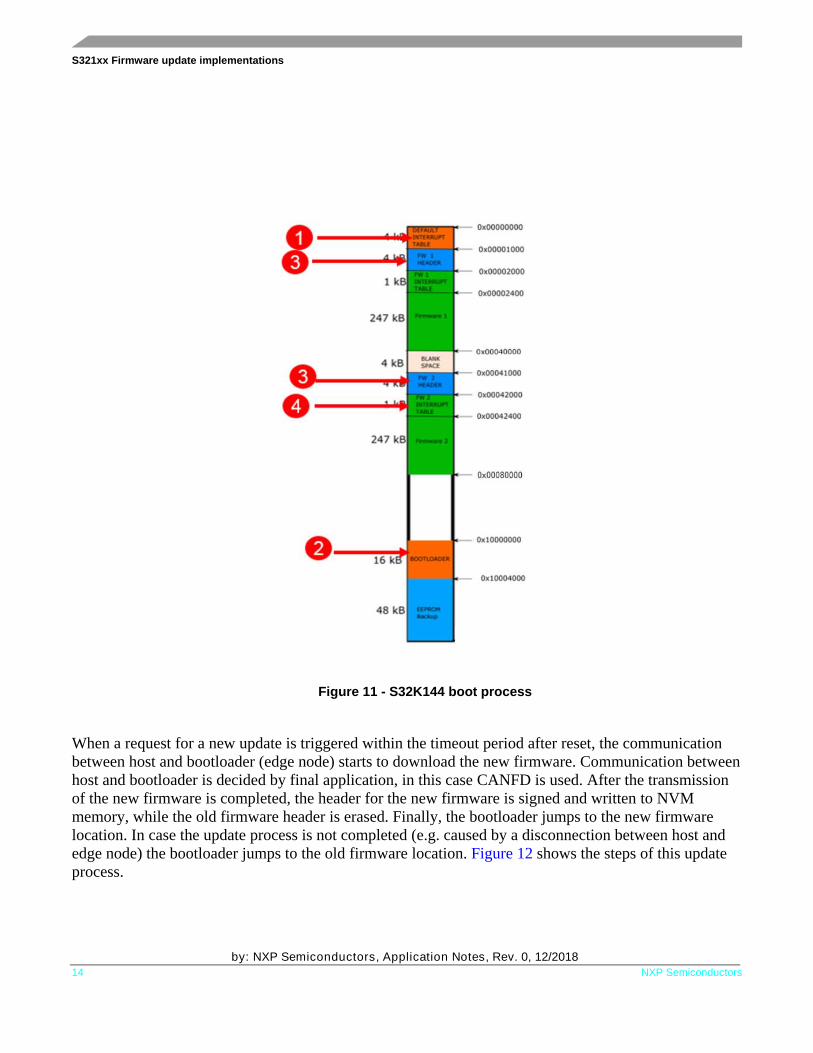
6.1.1 S32K144 Memory Map for A/B Swap, with single pflash block
In this case the S32K144 device is used to implement the a/b swap update in the device. Remembering
that S32K144 has a program flash of 512kB, and a flex memory of 64kB, in total there are two read
partitions available. The bootloader is loaded in a 16kB space from the flex memory. The program flash
locates the two applications images required for the a/b swap including a header for each one.
The header on each application function determines the firmware information. Information such as, but
not limited to, firmware version, oldest version, software developer details, size, author, app key could
be included in this header. After every update, the header information is also updated. The size of the
header is of 4kB, a program flash sector size. The header not only functions to store information of the
firmware running, but also to validate the latest firmware and if the firmware can be executed.
In the ARM® Cortex M cores, after a reset happens, core reads the first two words from the program
flash memory location, where the interrupt vector table is expected. The first word contains the stack
Figure 9 - S32K1xx memory sizes

S321xx Firmware update implementations
by: NXP Semiconductors, Application Notes, Rev. 0, 12/2018
12 NXP Semiconductors
pointer, and the second word contains the address of the reset handler. The core then sets the main stack
pointer address (SP) and the program counter (PC) to the start of the reset handler. Because of this initial
boot process of the core, it is necessary to preserve and not erase the first sector of the program flash. In
S32K144 the vector table size is 1kB long, hence given the sector size of the program flash, the initial
4kB of flash must not be erased.
For this case, the bootloader is allocated into flex memory area, so the second word in the pflash
contains the address that points to a flex memory address. Bootloader is placed on the flex memory
because it is a different read partition, that allows to execute commands that modify program flash
content without allocating the routine in RAM. Another benefit of allocating the bootloader in flex
memory, is that in S32K146 there are two read partitions of the program flash. Updates of a new
firmware can be done while the old firmware is still running.
The two applications are placed followed by its header. Between each of the applications, a gap of one
sector is left in blank. This is because the number of sectors remaining after considering the initial sector
for the default interrupt table, and two sectors for the firmware headers, is not even. Then each
application firmware image will have a size of 248kB or 62 sectors. The figure below shows a summary
of the resulting flash memory map.
Figure 10 - S32K144 memory map: A/B swap
S321xx Firmware update implementations
by: NXP Semiconductors, Application Notes, Rev. 0, 12/2018
NXP Semiconductors 13
6.1.2 S32K144 boot and update procedures
To determine the location of the oldest image in the program flash memory, the information on the
header is used. In this case, the validation of the header is done by checking if the firmware has a valid
app key sign, 0x55AA55AA, at the last header address. This signature of the header is the last step done
during an update procedure before jumping to the application. This key indicates that firmware update
was completed, and it is valid.
When the bootloader starts, it searches for the app key in the application header. It first reads the content
of the last address of the header one, if nothing is found in that location, then the new address to allocate
the upcoming firmware is that location. In case an app key is found in image one header, then the
content of the firmware header two is read, if no app key is found the new address to allocate the
upcoming firmware is image two location. When an app key is found in both headers, then the
firmware’s version is read to determine the oldest one. The location of the oldest firmware is then where
the upcoming firmware is allocated.
In case there is no update requested by a host within a defined timeout after reset (e.g. 4 seconds), the
bootloader jumps to the flash location with the newest firmware. For an eventual case in which neither
of the headers has the app key, this means that there is no valid firmware, the timeout is then
disregarded, and the bootloader stays waiting for update requests from the host. Figure 11 shows the
steps of the boot process.
Step 1. After Reset: fetch PC value @ 0x00000004.
Step 2. Bootloader starts.
Step 3. Bootloader searches for oldest and newest image.
- Check FW header information.
- Find app key (0x55AA55AA) at end of header.
- If no app key found in either header, stay in bootloader (i.e. do not jump to any application).
Step 4. After timeout: jump to newest application.
- Relocate VTOR table.
- PC fetch value from firmware interrupt table.
S321xx Firmware update implementations
by: NXP Semiconductors, Application Notes, Rev. 0, 12/2018
14 NXP Semiconductors
When a request for a new update is triggered within the timeout period after reset, the communication
between host and bootloader (edge node) starts to download the new firmware. Communication between
host and bootloader is decided by final application, in this case CANFD is used. After the transmission
of the new firmware is completed, the header for the new firmware is signed and written to NVM
memory, while the old firmware header is erased. Finally, the bootloader jumps to the new firmware
location. In case the update process is not completed (e.g. caused by a disconnection between host and
edge node) the bootloader jumps to the old firmware location. Figure 12 shows the steps of this update
process.
Figure 11 - S32K144 boot process
S321xx Firmware update implementations
by: NXP Semiconductors, Application Notes, Rev. 0, 12/2018
NXP Semiconductors 15
Step 1. After Reset: fetch PC value @ 0x00000004.
Step 2. Bootloader starts.
Step 3. Bootloader search for oldest and newest image.
- Check FW Header information.
- Find app key (0x55AA55AA) at end of header.
- Assign FW location to be updated (oldest).
Step 4. Update trigger received.
- Receive header first.
- Validate it is a new version.
- Start updating new firmware in oldest location.
Step 5. Update Completed.
- Update new firmware header.
- Erase/Update older firmware header.
Step 6. Jump to new application.
- Relocate VTOR table.
- PC fetch value from new firmware interrupt table.
S321xx Firmware update implementations
by: NXP Semiconductors, Application Notes, Rev. 0, 12/2018
16 NXP Semiconductors
6.2 S32K146 use case
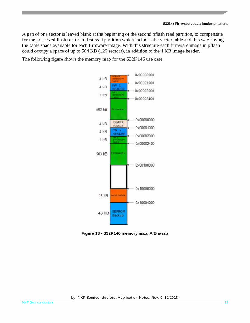
6.2.1 S32K146 memory map for A/B Swap, with dual pflash block
For this use case, an S32K146 is used to demonstrate the a/b swap update mechanism. The S32K146 has
1 MB of program flash memory, with two read partitions of 512 KB each and a flex memory space of 64
KB. The dual pflash read partition allows to erase/write one of the partitions while reading the other
partition or executing code from there. This means that the current firmware can continue to be executed
while the new firmware is being loaded. The bootloader is placed in a 16 KB space of the flex memory.
Just as with the S32K144 use case, two applications are loaded in the two pflash read partitions
correspondingly. Each firmware application includes a header with the firmware information (firmware
version, oldest version, software developer details, etc).
After a reset, the ARM Cortex M4 core takes the first two words from the vector table to initialize the
stack pointer (SP) and load the initial program counter (PC), which in this case is the entry point of the
bootloader located in flex memory. Due to this default ARM Cortex M4 boot process, the first flash
sector in which the vector table is located must be preserved.
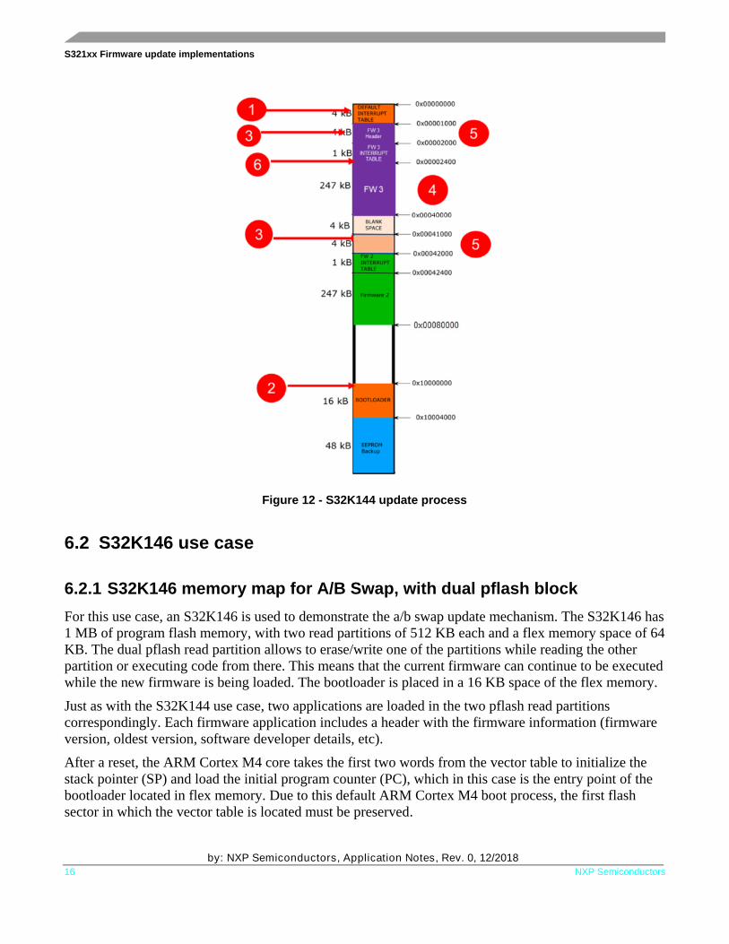
Figure 12 - S32K144 update process
S321xx Firmware update implementations
by: NXP Semiconductors, Application Notes, Rev. 0, 12/2018
NXP Semiconductors 17
A gap of one sector is leaved blank at the beginning of the second pflash read partition, to compensate
for the preserved flash sector in first read partition which includes the vector table and this way having
the same space available for each firmware image. With this structure each firmware image in pflash
could occupy a space of up to 504 KB (126 sectors), in addition to the 4 KB image header.
The following figure shows the memory map for the S32K146 use case.
Figure 13 - S32K146 memory map: A/B swap
S321xx Firmware update implementations
by: NXP Semiconductors, Application Notes, Rev. 0, 12/2018
18 NXP Semiconductors
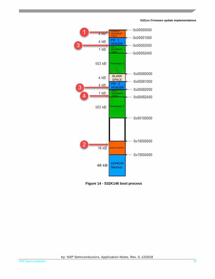
6.2.2 S32K146 boot and update procedures
Just as in the S32K144 use case, the information of each firmware header is used to determine the
location of the oldest image in program flash memory. This is performed by validating if the firmware
header has the valid app key sign (0x55AA55AA) at the last header address, which indicates that the
corresponding firmware is valid.
When the bootloader starts, it reads the firmware headers. The memory block to allocate an upcoming
new firmware is the one that has a header without a valid app key. If both headers have the valid app
key, then the firmware versions are compared to determine the location of the upcoming firmware. The
firmware with the oldest version will be the one overwritten.
The bootloader has a defined timeout after any reset (e.g. 2 seconds for S32K146 use case) waiting for
update requests commands from the host. If no request is received, the bootloader then jumps to the
flash location with the latest firmware. For the case of the bootloader not finding a valid app key in
either of the firmware headers, the timeout is disabled, and the bootloader keeps waiting for an update
request. Figure 14 shows the boot process for S32K146 use case.
Step 1. After Reset: fetch PC value @ 0x00000004.
Step 2. Bootloader starts.
Step 3. Bootloader searches for oldest and newest image.
- Check FW header information.
- Find app key (0x55AA55AA) at end of header.
- If no app key found in either header, stay in bootloader (i.e. do not jump to any application).
Step 4. After timeout: jump to newest application.
- Relocate VTOR table.
- PC fetch value from firmware interrupt table.
S321xx Firmware update implementations
by: NXP Semiconductors, Application Notes, Rev. 0, 12/2018
NXP Semiconductors 19
Figure 14 - S32K146 boot process
S321xx Firmware update implementations
by: NXP Semiconductors, Application Notes, Rev. 0, 12/2018
20 NXP Semiconductors
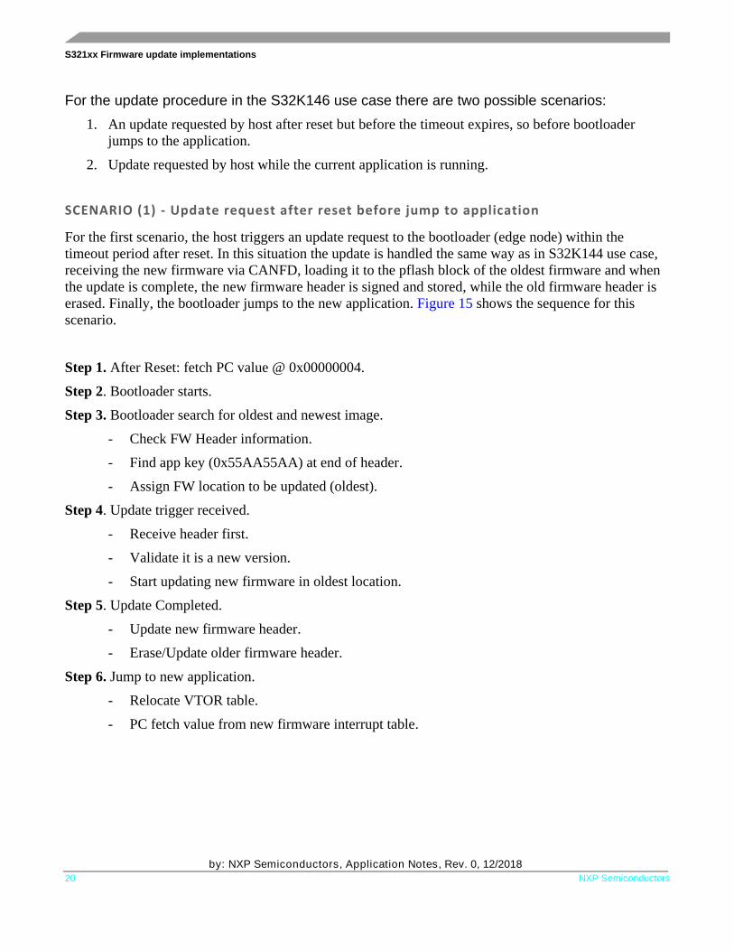
For the update procedure in the S32K146 use case there are two possible scenarios:
1. An update requested by host after reset but before the timeout expires, so before bootloader
jumps to the application.
2. Update requested by host while the current application is running.
SCENARIO (1) - Update request after reset before jump to application
For the first scenario, the host triggers an update request to the bootloader (edge node) within the
timeout period after reset. In this situation the update is handled the same way as in S32K144 use case,
receiving the new firmware via CANFD, loading it to the pflash block of the oldest firmware and when
the update is complete, the new firmware header is signed and stored, while the old firmware header is
erased. Finally, the bootloader jumps to the new application. Figure 15 shows the sequence for this
scenario.
Step 1. After Reset: fetch PC value @ 0x00000004.
Step 2. Bootloader starts.
Step 3. Bootloader search for oldest and newest image.
- Check FW Header information.
- Find app key (0x55AA55AA) at end of header.
- Assign FW location to be updated (oldest).
Step 4. Update trigger received.
- Receive header first.
- Validate it is a new version.
- Start updating new firmware in oldest location.
Step 5. Update Completed.
- Update new firmware header.
- Erase/Update older firmware header.
Step 6. Jump to new application.
- Relocate VTOR table.
- PC fetch value from new firmware interrupt table.
S321xx Firmware update implementations
by: NXP Semiconductors, Application Notes, Rev. 0, 12/2018
NXP Semiconductors 21
Figure 15 - S32K146 update process (scenario 1)
S321xx Firmware update implementations
by: NXP Semiconductors, Application Notes, Rev. 0, 12/2018
22 NXP Semiconductors
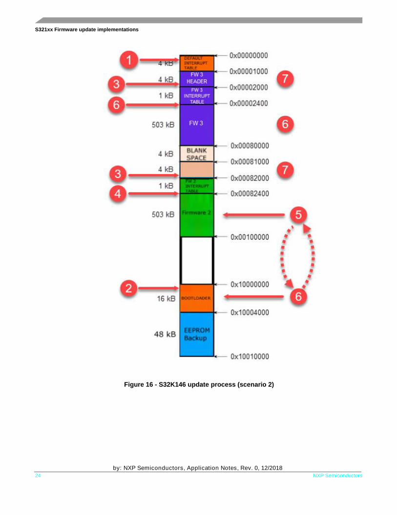
SCENARIO (2) - Update request while current application is running
In the second update scenario, the latest application is already running when an update request from the
host is received. To handle the update procedure without completely stopping the execution of the
current firmware, a mechanism to share the CPU processing time between bootloader and application is
required. The implementation of such mechanism is flexible, and the final application will determine the
appropriate balance between the processing time stolen from the application and the total time required
to complete a new firmware update. An important consideration is that the application software needs to
have some level of awareness of the bootloader, for example by initializing the communication interface
with the host, as well as including a way to give control to the bootloader so it can handle update
commands and data from the host.
For this reference implementation, the execution jumps from the application to the bootloader whenever
a new CANFD message with firmware data is received from the host. The data is processed and stored
in the corresponding pflash block, and execution jumps back to the application at the same point where
it was halted. The loader dedicated entry address is shared with the application so that it knows where to
jump when receiving commands from the host. The application-bootloader jumping loop continues until
the update process is completed. At this point the bootloader informs of the completion status to the
application using a status variable in SRAM memory, then the application triggers a software reset to
launch the new firmware version. Figure 16 shows the overall procedure for this update scenario.
S321xx Firmware update implementations
by: NXP Semiconductors, Application Notes, Rev. 0, 12/2018
NXP Semiconductors 23
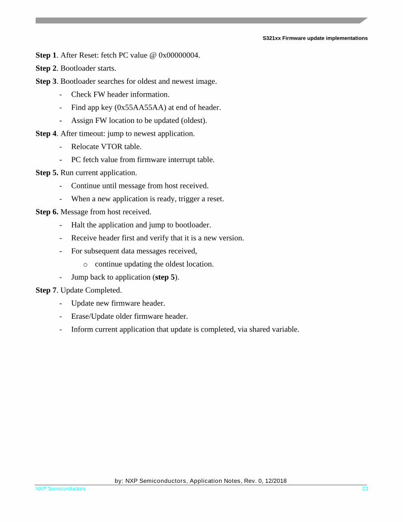
Step 1. After Reset: fetch PC value @ 0x00000004.
Step 2. Bootloader starts.
Step 3. Bootloader searches for oldest and newest image.
- Check FW header information.
- Find app key (0x55AA55AA) at end of header.
- Assign FW location to be updated (oldest).
Step 4. After timeout: jump to newest application.
- Relocate VTOR table.
- PC fetch value from firmware interrupt table.
Step 5. Run current application.
- Continue until message from host received.
- When a new application is ready, trigger a reset.
Step 6. Message from host received.
- Halt the application and jump to bootloader.
- Receive header first and verify that it is a new version.
- For subsequent data messages received,
o continue updating the oldest location.
- Jump back to application (step 5).
Step 7. Update Completed.
- Update new firmware header.
- Erase/Update older firmware header.
- Inform current application that update is completed, via shared variable.
S321xx Firmware update implementations
by: NXP Semiconductors, Application Notes, Rev. 0, 12/2018
24 NXP Semiconductors
Figure 16 - S32K146 update process (scenario 2)
S321xx Firmware update implementations
by: NXP Semiconductors, Application Notes, Rev. 0, 12/2018
NXP Semiconductors 25
6.3 A/B swap using Position Independent Code (PIC)
After the update process, there will be two firmware images located in the program flash memory.
Images are in different physical addresses of the flash memory. To be able to execute the code at the
specific address, each firmware linker should be modified to indicate the location in where it will be
placed. It might be difficult to keep track of the location of where the new firmware will be placed for
each of the devices that are in the field. Therefore, it is convenient to be able to execute the code
regardless of its address on the program flash.
Position independent code means that the firmware executes regardless of its absolute address in
memory, meaning that there won’t be absolute jumps within the code. This allows developing firmware
without the need of modifying the linker file, and firmware can run from any pflash memory address in
where it is placed.
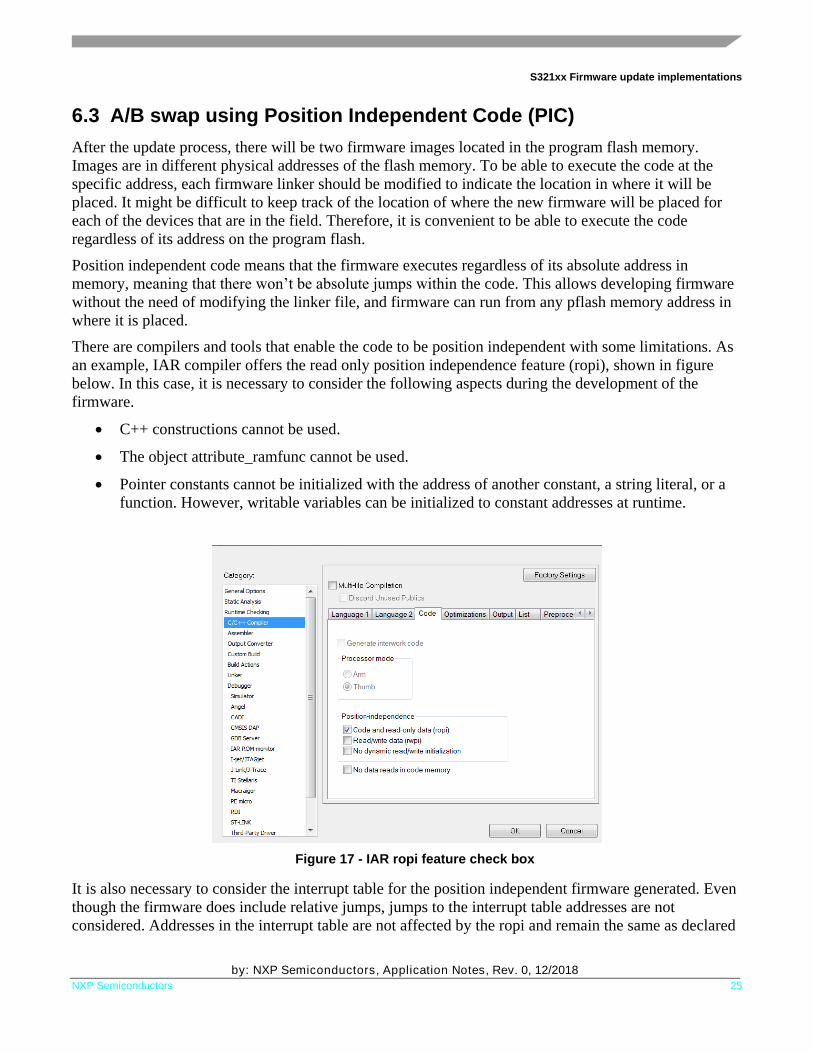
There are compilers and tools that enable the code to be position independent with some limitations. As
an example, IAR compiler offers the read only position independence feature (ropi), shown in figure
below. In this case, it is necessary to consider the following aspects during the development of the
firmware.
• C++ constructions cannot be used.
• The object attribute_ramfunc cannot be used.
• Pointer constants cannot be initialized with the address of another constant, a string literal, or a
function. However, writable variables can be initialized to constant addresses at runtime.
It is also necessary to consider the interrupt table for the position independent firmware generated. Even
though the firmware does include relative jumps, jumps to the interrupt table addresses are not
considered. Addresses in the interrupt table are not affected by the ropi and remain the same as declared
Figure 17 - IAR ropi feature check box
S321xx Firmware update implementations
by: NXP Semiconductors, Application Notes, Rev. 0, 12/2018
26 NXP Semiconductors
in the linker file. To solve this, the interrupt is located starting at address 0x00000000 as by default in
the linker file, and then an offset address must be added to each entry of the interrupt table during the
update process, except for the first entry that is the stack pointer. The address offset value depends on
where the new firmware will be in program flash. Hence, when an interrupt happens, core jumps to the
exact location in program flash where the application firmware is placed.
6.4 Communication process
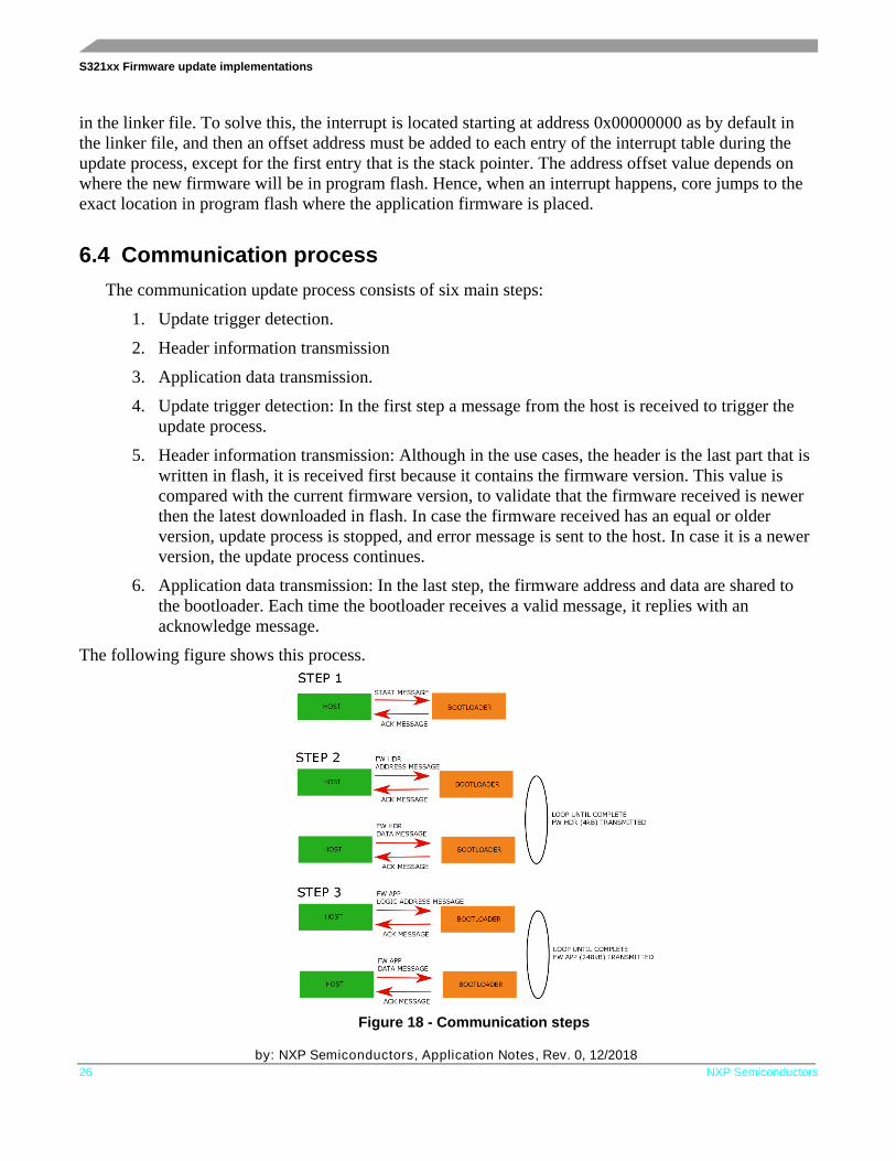
The communication update process consists of six main steps:
1. Update trigger detection.
2. Header information transmission
3. Application data transmission.
4. Update trigger detection: In the first step a message from the host is received to trigger the
update process.
5. Header information transmission: Although in the use cases, the header is the last part that is
written in flash, it is received first because it contains the firmware version. This value is
compared with the current firmware version, to validate that the firmware received is newer
then the latest downloaded in flash. In case the firmware received has an equal or older
version, update process is stopped, and error message is sent to the host. In case it is a newer
version, the update process continues.
6. Application data transmission: In the last step, the firmware address and data are shared to
the bootloader. Each time the bootloader receives a valid message, it replies with an
acknowledge message.
The following figure shows this process.
Figure 18 - Communication steps
S321xx Firmware update implementations
by: NXP Semiconductors, Application Notes, Rev. 0, 12/2018
NXP Semiconductors 27
6.5 Secure communication
During the update process, the firmware that is shared between the host and bootloader is vulnerable to
attacks. A possible attack can sniff the network to steal the intellectual property of the firmware.
Another possible attack is to send an unauthorized firmware from and unauthorized host to the
bootloader, to manipulate the final application. To avoid eavesdrop, replication attack, and ensure that
firmware is coming from an authentic source, a secure communication must be established between host
and bootloader. In the case of S32K1xx devices this is possible due the inclusion of the CSEc module.
Eavesdropping attack, is the situation in which an attacker sniffs the network to obtain the firmware that
is shared. Then, the data can be used by the attacker to re program other non-authorized modules using
the firmware or steal the intellectual property. To avoid this attack, the data shared in the update process
is encrypted. The host encrypts firmware’s data using AES-128 CBC algorithm, with a secret key
before it sends it to the bootloader. Bootloader receives this data and decrypts it using the same known
key. Key is not shared during the update process, and it is previously stored on each device in an offline
manner.
Using encryption of the data, the confidentiality of the firmware is protected. Next step to consider is the
integrity and the authentication of the message that is been share. An unauthorized host can send data to
the bootloader, to download data into the bootloader flash that will cause a malfunctioning of the device.
To authenticate the source of the message, and that the message has not been modified, a CMAC value
is used.
A CMAC value per each message is generated form the host using a known key, and the data to share.
When the bootloader receives a new message with firmware data, it calculates the CMAC value for the
received data using the same key as the host. After bootloaders calculates the CMAC, it compares it
with the received CMAC. In case the CMAC verification is correct, the message received is considered
valid. If the CMAC values are different, it indicates that either it is not coming from the authorized
source or the data got corrupted. Hence, the message is considered as invalid and data is not downloaded
to flash.
Besides the confidentially and the authenticity of the message received, the freshness of the message
should be considered to avoid reply attacks. A potential attacker can send the same messages, obtained
by sniffing the network, several times to the bootloader causing an unwanted functionality of the device.
To prevent this attack, a random number can be shared in every message between bootloader and host.
The CSEc module includes two random number generators, that can be used for this purpose.
The CSEc random number generators are a true random number generator (TRNG) and pseudo random
generator (PRNG). The TRNG is used to generate the seed, that is later used for the PRNG to generate
random number using a CSEc command. The random number generator should be initialized after every
reset; hence a new random seed is used.
For the update process, bootloader generates a random number and shares it with the host to avoid the
reply attack. Bootloader sends a plain random number to the host, host then receives this number and
encrypts it using CBC and a known key. Next time the host sends data to the bootloader, it adds the
encrypted random number together with the firmware data and CMAC. Then, the bootloader receives
the message and decrypts the random number. If the random number decrypted is same as the one that
was previously shared the message is fresh and valid, otherwise the message can be considered invalid.
S321xx Firmware update implementations
by: NXP Semiconductors, Application Notes, Rev. 0, 12/2018
28 NXP Semiconductors
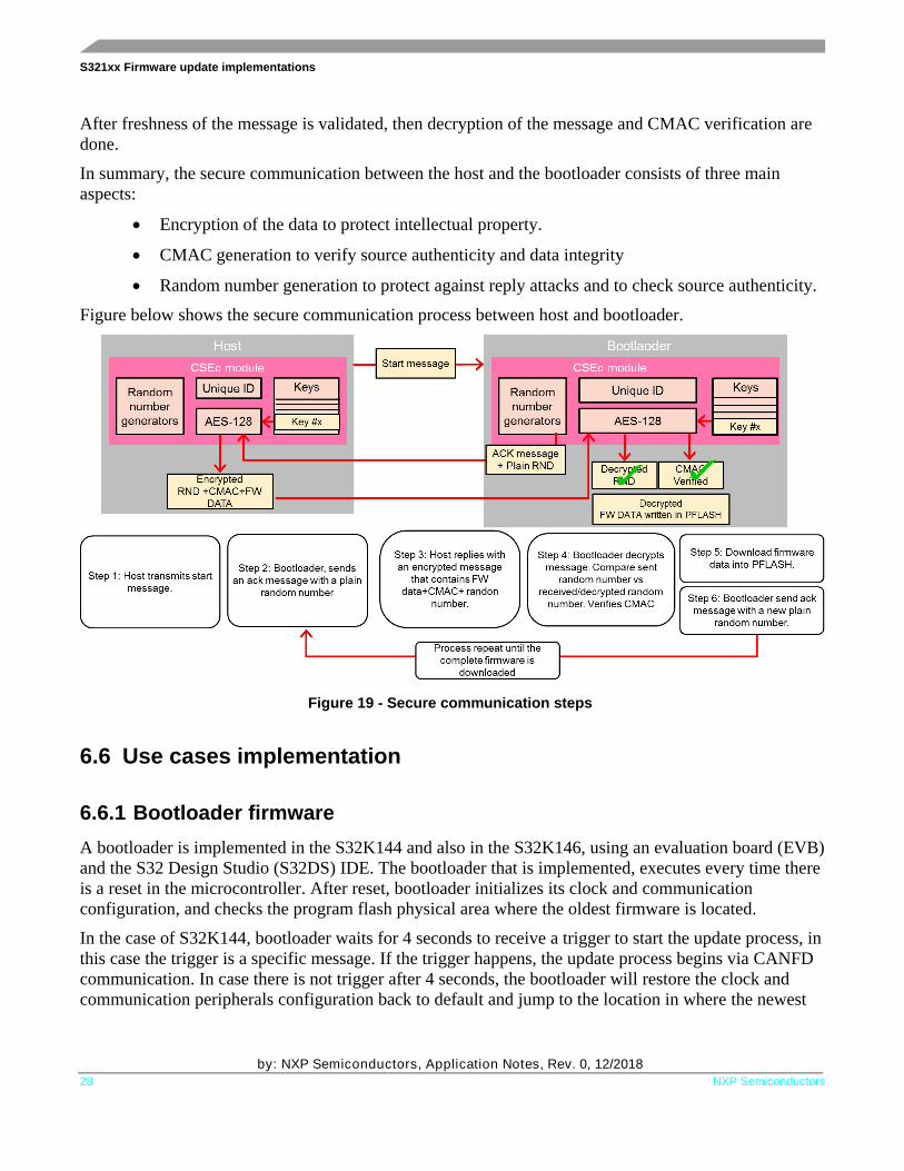
After freshness of the message is validated, then decryption of the message and CMAC verification are
done.
In summary, the secure communication between the host and the bootloader consists of three main
aspects:
• Encryption of the data to protect intellectual property.
• CMAC generation to verify source authenticity and data integrity
• Random number generation to protect against reply attacks and to check source authenticity.
Figure below shows the secure communication process between host and bootloader.
6.6 Use cases implementation
6.6.1 Bootloader firmware
A bootloader is implemented in the S32K144 and also in the S32K146, using an evaluation board (EVB)
and the S32 Design Studio (S32DS) IDE. The bootloader that is implemented, executes every time there
is a reset in the microcontroller. After reset, bootloader initializes its clock and communication
configuration, and checks the program flash physical area where the oldest firmware is located.
In the case of S32K144, bootloader waits for 4 seconds to receive a trigger to start the update process, in
this case the trigger is a specific message. If the trigger happens, the update process begins via CANFD
communication. In case there is not trigger after 4 seconds, the bootloader will restore the clock and
communication peripherals configuration back to default and jump to the location in where the newest
Figure 19 - Secure communication steps
S321xx Firmware update implementations
by: NXP Semiconductors, Application Notes, Rev. 0, 12/2018
NXP Semiconductors 29
firmware is located. For a trigger message to be detected, the S32K144 needs to be reset, so the 4
seconds period starts again.
For S32K146, the bootloader only waits for 2 seconds to receive a trigger, then restores the clocks and
communication peripherals, finally jumping to the newest application. A trigger message can be sent
from the gateway to initiate the update process while the current firmware is executing. For this purpose,
the application in turn should initialize the communication peripheral so it is ready to receive messages
from the host.
The bootloader is placed in the first 16kB of the flex memory area. The S32K144 or S32K146 is
previously partitioned to work as EEPROM backup in which 16kB are reserved for data flash
(bootloader execution), while the other 48kB are used for EEPROM data backup and key storage for the
CSEc.
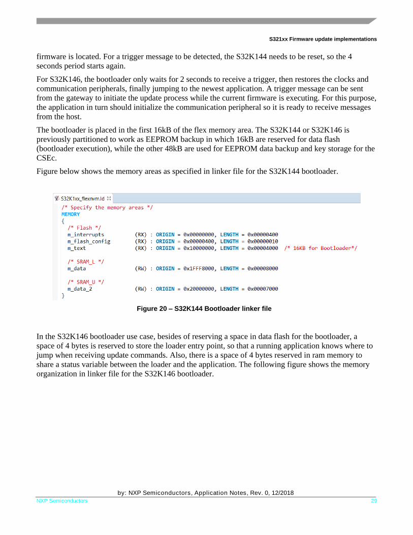
Figure below shows the memory areas as specified in linker file for the S32K144 bootloader.
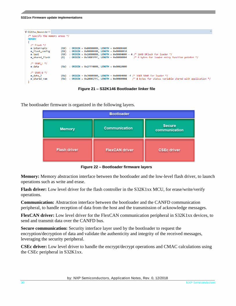
In the S32K146 bootloader use case, besides of reserving a space in data flash for the bootloader, a
space of 4 bytes is reserved to store the loader entry point, so that a running application knows where to
jump when receiving update commands. Also, there is a space of 4 bytes reserved in ram memory to
share a status variable between the loader and the application. The following figure shows the memory
organization in linker file for the S32K146 bootloader.
Figure 20 – S32K144 Bootloader linker file
S321xx Firmware update implementations
by: NXP Semiconductors, Application Notes, Rev. 0, 12/2018
30 NXP Semiconductors
The bootloader firmware is organized in the following layers.
Memory: Memory abstraction interface between the bootloader and the low-level flash driver, to launch
operations such as write and erase.
Flash driver: Low level driver for the flash controller in the S32K1xx MCU, for erase/write/verify
operations.
Communication: Abstraction interface between the bootloader and the CANFD communication
peripheral, to handle reception of data from the host and the transmission of acknowledge messages.
FlexCAN driver: Low level driver for the FlexCAN communication peripheral in S32K1xx devices, to
send and transmit data over the CANFD bus.
Secure communication: Security interface layer used by the bootloader to request the
encryption/decryption of data and validate the authenticity and integrity of the received messages,
leveraging the security peripheral.
CSEc driver: Low level driver to handle the encrypt/decrypt operations and CMAC calculations using
the CSEc peripheral in S32K1xx.
Figure 21 – S32K146 Bootloader linker file
Figure 22 – Bootloader firmware layers

S321xx Firmware update implementations
by: NXP Semiconductors, Application Notes, Rev. 0, 12/2018
NXP Semiconductors 31
6.6.2 CANFD communication
The bootloader supports CANFD communication protocol, to execute the update process. CANFD
standard bit rate is of 500kbps, and the fast bit rate is 2 Mbps.
Four types of messages are transmitted, each one with an associated ID.
• Start of update process.
• Address of the firmware/ header data.
• Firmware’s or header’s data.
• Acknowledge/error message.
The start messages, triggers the update process, it has an ID of 0x200, and its payload are 4 bytes with
the value 0x15151515. The address message, transmit either the logical address of the firmware or the
header address, its ID is 0x100, the payload size is of 4B. The end of data message indicates that all the
data for the firmware or header has been sent, it’s ID is same as the address message, but the payload
contains a unique value of 0x53535353. The firmware or header data message, contains the data that
will be downloaded to the flash, it’s ID is 0x300, the payload size is 32B.
These messages are transmitted from the host to the bootloader, but bootloader also transmits a message
of acknowledge or error. The acknowledge message, indicates that the previous message was correctly
received, it’s ID is 0x400 and the payload size is of 4B with the value 0x04040404. The message error,
indicates that something went wrong when received the message or the firmware version received is not
the latest one, it’s ID is also 0x400 and the payload size is of 4B with the value 0x55555555. The table
below summarizes the messages ID and payloads.
Table 2 Communication messages
Message ID Payload Size Payload Direction Description
Start 0x200 4 0x15151515 HOST -> BOOTLOADER Triggers update process
Address 0x100 4 Address of firmware header
or firmware logic address
End of data: 0x53535353 HOST -> BOOTLOADER
Contains the address for
the fw hdr information or
the logic address of the
fw application.
Contains end of data
payload.
Data 0x300 32 Firmware header or
firmware application data. HOST -> BOOTLOADER
Contains firmware
header or firmware
application data., that is
downloaded to pflash.
Ack 0x400 4 Acknowledge payload:
0x04040404
Error payload:
0x55555555
BOOTLOADER -> HOST
Contains acknowledge
payload.
Contains error payload.
S321xx Firmware update implementations
by: NXP Semiconductors, Application Notes, Rev. 0, 12/2018
32 NXP Semiconductors
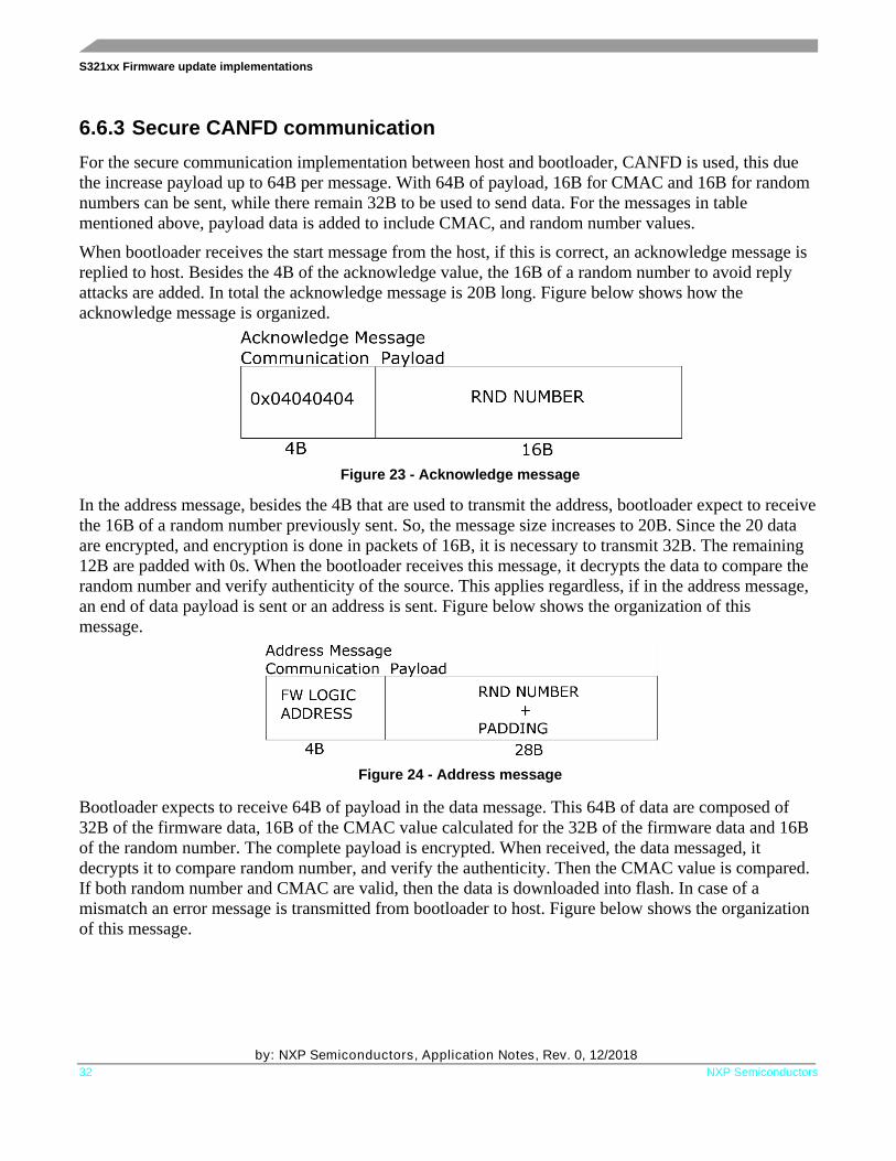
6.6.3 Secure CANFD communication
For the secure communication implementation between host and bootloader, CANFD is used, this due
the increase payload up to 64B per message. With 64B of payload, 16B for CMAC and 16B for random
numbers can be sent, while there remain 32B to be used to send data. For the messages in table
mentioned above, payload data is added to include CMAC, and random number values.
When bootloader receives the start message from the host, if this is correct, an acknowledge message is
replied to host. Besides the 4B of the acknowledge value, the 16B of a random number to avoid reply
attacks are added. In total the acknowledge message is 20B long. Figure below shows how the
acknowledge message is organized.
In the address message, besides the 4B that are used to transmit the address, bootloader expect to receive
the 16B of a random number previously sent. So, the message size increases to 20B. Since the 20 data
are encrypted, and encryption is done in packets of 16B, it is necessary to transmit 32B. The remaining
12B are padded with 0s. When the bootloader receives this message, it decrypts the data to compare the
random number and verify authenticity of the source. This applies regardless, if in the address message,
an end of data payload is sent or an address is sent. Figure below shows the organization of this
message.
Bootloader expects to receive 64B of payload in the data message. This 64B of data are composed of
32B of the firmware data, 16B of the CMAC value calculated for the 32B of the firmware data and 16B
of the random number. The complete payload is encrypted. When received, the data messaged, it
decrypts it to compare random number, and verify the authenticity. Then the CMAC value is compared.
If both random number and CMAC are valid, then the data is downloaded into flash. In case of a
mismatch an error message is transmitted from bootloader to host. Figure below shows the organization
of this message.
Figure 23 - Acknowledge message
Figure 24 - Address message
Demo
by: NXP Semiconductors, Application Notes, Rev. 0, 12/2018
NXP Semiconductors 33
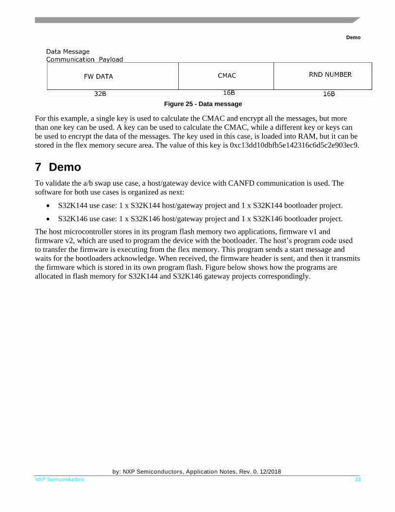
For this example, a single key is used to calculate the CMAC and encrypt all the messages, but more
than one key can be used. A key can be used to calculate the CMAC, while a different key or keys can
be used to encrypt the data of the messages. The key used in this case, is loaded into RAM, but it can be
stored in the flex memory secure area. The value of this key is 0xc13dd10dbfb5e142316c6d5c2e903ec9.
7 Demo
To validate the a/b swap use case, a host/gateway device with CANFD communication is used. The
software for both use cases is organized as next:
• S32K144 use case: 1 x S32K144 host/gateway project and 1 x S32K144 bootloader project.
• S32K146 use case: 1 x S32K146 host/gateway project and 1 x S32K146 bootloader project.
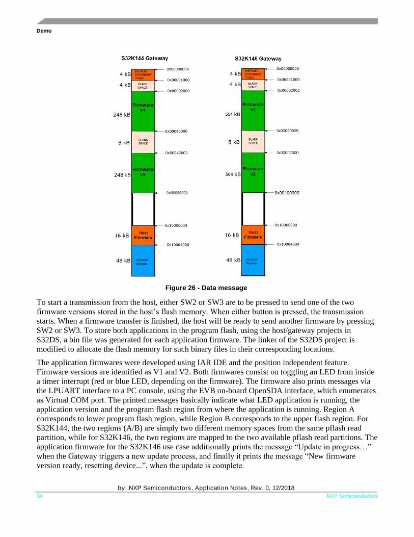
The host microcontroller stores in its program flash memory two applications, firmware v1 and
firmware v2, which are used to program the device with the bootloader. The host’s program code used
to transfer the firmware is executing from the flex memory. This program sends a start message and
waits for the bootloaders acknowledge. When received, the firmware header is sent, and then it transmits
the firmware which is stored in its own program flash. Figure below shows how the programs are
allocated in flash memory for S32K144 and S32K146 gateway projects correspondingly.
Figure 25 - Data message
Demo
by: NXP Semiconductors, Application Notes, Rev. 0, 12/2018
34 NXP Semiconductors
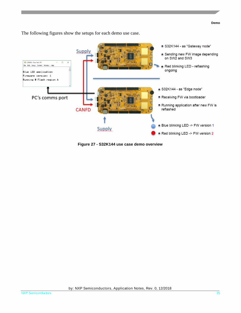
To start a transmission from the host, either SW2 or SW3 are to be pressed to send one of the two
firmware versions stored in the host’s flash memory. When either button is pressed, the transmission
starts. When a firmware transfer is finished, the host will be ready to send another firmware by pressing
SW2 or SW3. To store both applications in the program flash, using the host/gateway projects in
S32DS, a bin file was generated for each application firmware. The linker of the S32DS project is
modified to allocate the flash memory for such binary files in their corresponding locations.
The application firmwares were developed using IAR IDE and the position independent feature.
Firmware versions are identified as V1 and V2. Both firmwares consist on toggling an LED from inside
a timer interrupt (red or blue LED, depending on the firmware). The firmware also prints messages via
the LPUART interface to a PC console, using the EVB on-board OpenSDA interface, which enumerates
as Virtual COM port. The printed messages basically indicate what LED application is running, the
application version and the program flash region from where the application is running. Region A
corresponds to lower program flash region, while Region B corresponds to the upper flash region. For
S32K144, the two regions (A/B) are simply two different memory spaces from the same pflash read
partition, while for S32K146, the two regions are mapped to the two available pflash read partitions. The
application firmware for the S32K146 use case additionally prints the message “Update in progress…”
when the Gateway triggers a new update process, and finally it prints the message “New firmware
version ready, resetting device...”, when the update is complete.
Figure 26 - Data message
Demo
by: NXP Semiconductors, Application Notes, Rev. 0, 12/2018
NXP Semiconductors 35
The following figures show the setups for each demo use case.
Figure 27 - S32K144 use case demo overview
Demo
by: NXP Semiconductors, Application Notes, Rev. 0, 12/2018
36 NXP Semiconductors
7.1 Setting up the demo
This section describes the setup for each bootloader use case demo. The corresponding S32 Design
Studio projects and the IAR application projects are included as a software package together with this
application note.
7.1.1 Setting up S32K144 bootloader demo
The workspace OTA_S32K144_Use_Case_WS includes the following projects:
• S32K144_Memory_Partition: This project setups the flex memory of the S32K144, to be 48
KB of EEPROM backup and 16 KB for code.
• S32K144_FOTA_Bootloader: This project is the bootloader for the S32K144 edge node
microcontroller
• S32K144_FOTA_Gateway: This project is for the S32K144 device acting as a host/gateway.
The project includes two binary files of the precompiled application firmwares (v1/v2).
The following hardware is required:
• 2 x S32K144 EVB boards.
• 4 x female-to-female jumper cables.
• 1 x micro USB cable.
• 1 x 12 V power supply.
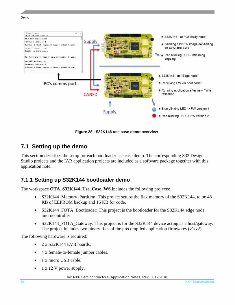
Figure 28 - S32K146 use case demo overview
Demo
by: NXP Semiconductors, Application Notes, Rev. 0, 12/2018
NXP Semiconductors 37
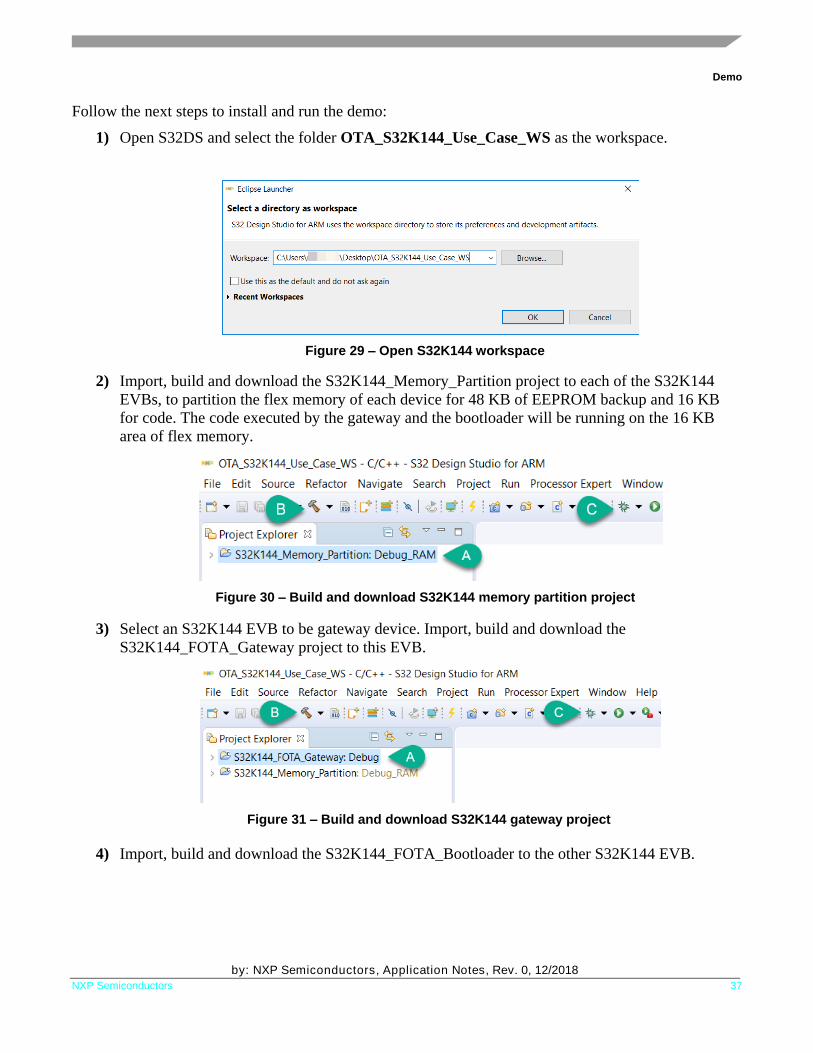
Follow the next steps to install and run the demo:
1) Open S32DS and select the folder OTA_S32K144_Use_Case_WS as the workspace.
2) Import, build and download the S32K144_Memory_Partition project to each of the S32K144
EVBs, to partition the flex memory of each device for 48 KB of EEPROM backup and 16 KB
for code. The code executed by the gateway and the bootloader will be running on the 16 KB
area of flex memory.
3) Select an S32K144 EVB to be gateway device. Import, build and download the
S32K144_FOTA_Gateway project to this EVB.
4) Import, build and download the S32K144_FOTA_Bootloader to the other S32K144 EVB.
Figure 29 – Open S32K144 workspace
Figure 30 – Build and download S32K144 memory partition project
Figure 31 – Build and download S32K144 gateway project
Demo
by: NXP Semiconductors, Application Notes, Rev. 0, 12/2018
38 NXP Semiconductors
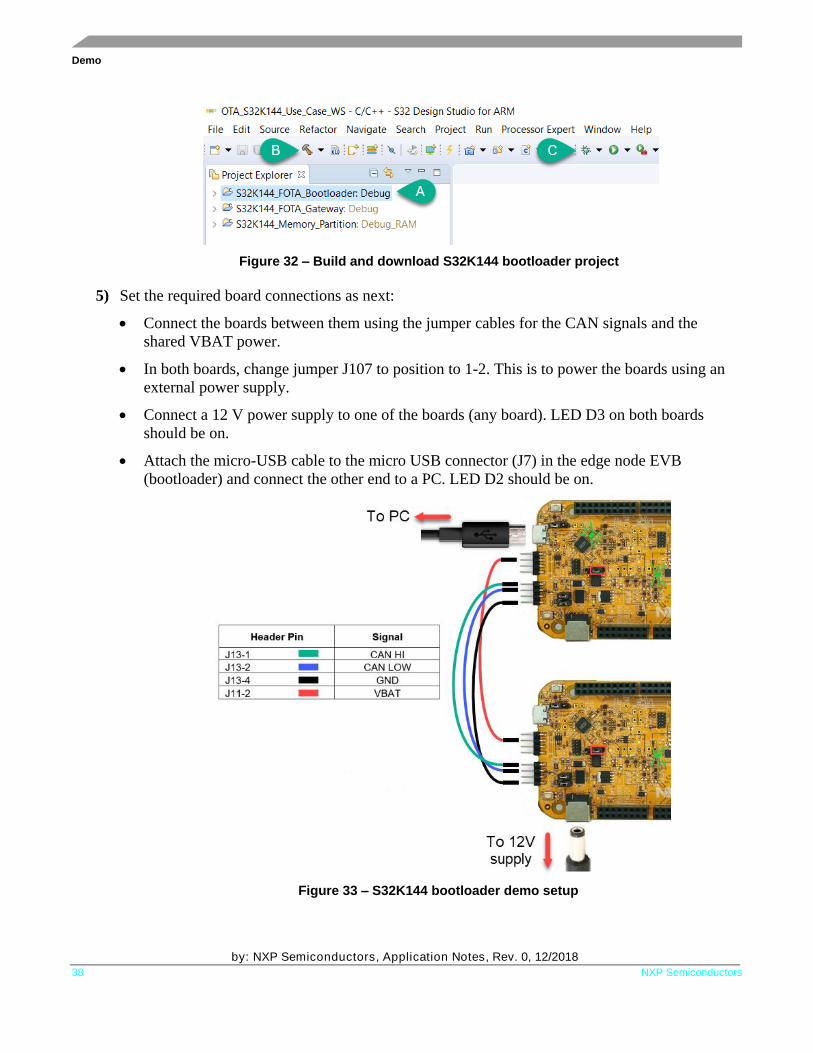
5) Set the required board connections as next:
• Connect the boards between them using the jumper cables for the CAN signals and the
shared VBAT power.
• In both boards, change jumper J107 to position to 1-2. This is to power the boards using an
external power supply.
• Connect a 12 V power supply to one of the boards (any board). LED D3 on both boards
should be on.
• Attach the micro-USB cable to the micro USB connector (J7) in the edge node EVB
(bootloader) and connect the other end to a PC. LED D2 should be on.
Figure 32 – Build and download S32K144 bootloader project
Figure 33 – S32K144 bootloader demo setup

Demo
by: NXP Semiconductors, Application Notes, Rev. 0, 12/2018
NXP Semiconductors 39
6) Open a serial terminal, select the OpenSDA virtual COM and set the terminal to a baud rate of
9600.
7) Reset the edge node EVB (bootloader board) by pressing the reset button SW5.
8) Before the 4 seconds timeout expires, press SW2 (for blue LED, v1 firmware) or SW3 (for red
LED, v2 firmware) in the gateway board.
9) Once update is complete, the LED corresponding to firmware version in the edge node will start
blinking, and the terminal will show the new firmware information.
7.1.2 Setting up S32K146 bootloader demo
The workspace OTA_S32K146_Use_Case_WS includes the following projects:
• S32K146_Memory_Partition: This project setups the flex memory of the S32K146, to be 48
KB of EEPROM backup and 16 KB for code.
• S32K146_FOTA_Bootloader: This project is the bootloader for the S32K146 edge node
microcontroller
• S32K146_FOTA_Gateway: This project is for the S32K146 device acting as a host/gateway.
The project includes two binary files of the precompiled application firmwares (v1/v2).
The following hardware is required:
• 2 x S32K146 EVB boards.
• 4 x female-to-female jumper cables.
• 1 x micro USB cable.
• 1 x 12 V power supply.
Follow the next procedure to install and run the demo:
1) Open S32DS and select the folder OTA_S32K146_Use_Case_WS as the workspace.
Figure 34 – Open S32K146 workspace
Demo
by: NXP Semiconductors, Application Notes, Rev. 0, 12/2018
40 NXP Semiconductors
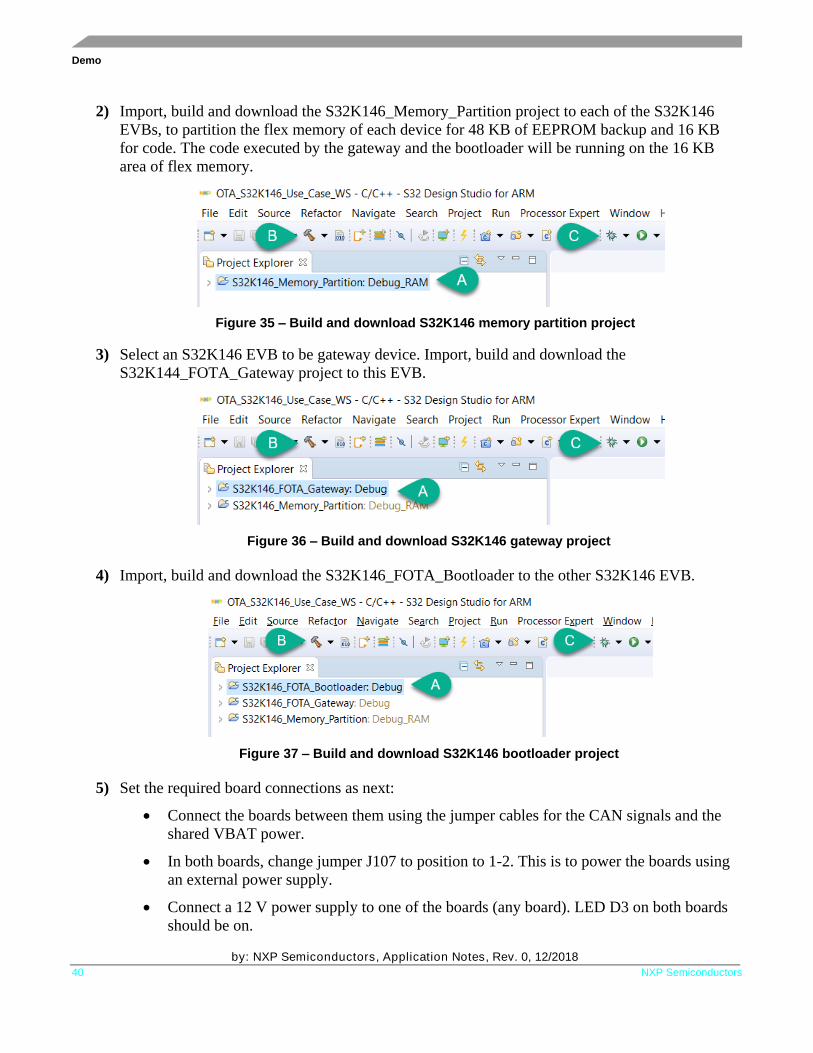
2) Import, build and download the S32K146_Memory_Partition project to each of the S32K146
EVBs, to partition the flex memory of each device for 48 KB of EEPROM backup and 16 KB
for code. The code executed by the gateway and the bootloader will be running on the 16 KB
area of flex memory.
3) Select an S32K146 EVB to be gateway device. Import, build and download the
S32K144_FOTA_Gateway project to this EVB.
4) Import, build and download the S32K146_FOTA_Bootloader to the other S32K146 EVB.
5) Set the required board connections as next:
• Connect the boards between them using the jumper cables for the CAN signals and the
shared VBAT power.
• In both boards, change jumper J107 to position to 1-2. This is to power the boards using
an external power supply.
• Connect a 12 V power supply to one of the boards (any board). LED D3 on both boards
should be on.
Figure 35 – Build and download S32K146 memory partition project
Figure 36 – Build and download S32K146 gateway project
Figure 37 – Build and download S32K146 bootloader project
Demo
by: NXP Semiconductors, Application Notes, Rev. 0, 12/2018
NXP Semiconductors 41
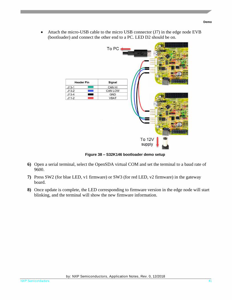
• Attach the micro-USB cable to the micro USB connector (J7) in the edge node EVB
(bootloader) and connect the other end to a PC. LED D2 should be on.
6) Open a serial terminal, select the OpenSDA virtual COM and set the terminal to a baud rate of
9600.
7) Press SW2 (for blue LED, v1 firmware) or SW3 (for red LED, v2 firmware) in the gateway
board.
8) Once update is complete, the LED corresponding to firmware version in the edge node will start
blinking, and the terminal will show the new firmware information.
Figure 38 – S32K146 bootloader demo setup

References
by: NXP Semiconductors, Application Notes, Rev. 0, 12/2018
42 NXP Semiconductors
8 References
• S32K Family Reference Manual
• Position independent code with IAR
• Merging a binary file into a S32 Design Studio project using linker commands


Document Number: AN12323 Rev. 0
12/2018
How to Reach Us:
Home Page:
nxp.com
Web Support:
nxp.com/support
Information in this document is provided solely to enable system and software
implementers to use NXP products. There are no express or implied copyright licenses
granted hereunder to design or fabricate any integrated circuits based on the
information in this document. NXP reserves the right to make changes without further
notice to any products herein.
NXP makes no warranty, representation, or guarantee regarding the suitability of its
products for any particular purpose, nor does NXP assume any liability arising out of the
application or use of any product or circuit, and specifically disclaims any and all
liability, including without limitation consequential or incidental damages. “Typical”
parameters that may be provided in NXP data sheets and/or specifications can and do
vary in different applications, and actual performance may vary over time. All operating
parameters, including “typicals,” must be validated for each customer application by
customer’s technical experts. NXP does not convey any license under its patent rights
nor the rights of others. NXP sells products pursuant to standard terms and conditions
of sale, which can be found at the following address: nxp.com/SalesTermsandConditions.
While NXP has implemented advanced security features, all products may be subject to
unidentified vulnerabilities. Customers are responsible for the design and operation of
their applications and products to reduce the effect of these vulnerabilities on
customer's applications and products, and NXP accepts no liability for any vulnerability
that is discovered. Customers should implement appropriate design and operating
safeguards to minimize the risks associated with their applications and products.
NXP, the NXP logo, NXP SECURE CONNECTIONS FOR A SMARTER WORLD,
COOLFLUX, EMBRACE, GREENCHIP, HITAG, I2C BUS, ICODE, JCOP, LIFE VIBES,
MIFARE, MIFARE CLASSIC, MIFARE DESFire, MIFARE PLUS, MIFARE FLEX,
MANTIS, MIFARE ULTRALIGHT, MIFARE4MOBILE, MIGLO, NTAG, ROADLINK,
SMARTLX, SMARTMX, STARPLUG, TOPFET, TRENCHMOS, UCODE, Freescale, the
Freescale logo, AltiVec, C 5, CodeTEST, CodeWarrior, ColdFire, ColdFire+, C Ware,
the Energy Efficient Solutions logo, Kinetis, Layerscape, MagniV, mobileGT, PEG,
PowerQUICC, Processor Expert, QorIQ, QorIQ Qonverge, Ready Play, SafeAssure, the
SafeAssure logo, StarCore, Symphony, VortiQa, Vybrid, Airfast, BeeKit, BeeStack,
CoreNet, Flexis, MXC, Platform in a Package, QUICC Engine, SMARTMOS, Tower,
TurboLink, and UMEMS are trademarks of NXP B.V. All other product or service names
are the property of their respective owners. ARM, AMBA, ARM Powered, Artisan,
Cortex, Jazelle, Keil, SecurCore, Thumb, TrustZone, and μVision are registered
trademarks of ARM Limited (or its subsidiaries) in the EU and/or elsewhere. ARM7,
ARM9, ARM11, big.LITTLE, CoreLink, CoreSight, DesignStart, Mali, mbed, NEON,
POP, Sensinode, Socrates, ULINK and Versatile are trademarks of ARM Limited (or its
subsidiaries) in the EU and/or elsewhere. All rights reserved. Oracle and Java are
registered trademarks of Oracle and/or its affiliates. The Power Architecture and
Power.org word marks and the Power and Power.org logos and related marks are
trademarks and service marks licensed by Power.org.
© 2018 NXP B.V.
.