Embed Size (px)
Citation preview

Important notice Dear Customer, On 7 February 2017 the former NXP Standard Product business became a new company with the tradename Nexperia. Nexperia is an industry leading supplier of Discrete, Logic and PowerMOS semiconductors with its focus on the automotive, industrial, computing, consumer and wearable application markets In data sheets and application notes which still contain NXP or Philips Semiconductors references, use the references to Nexperia, as shown below. Instead of http://www.nxp.com, http://www.philips.com/ or http://www.semiconductors.philips.com/, use http://www.nexperia.com Instead of [email protected] or [email protected], use [email protected] (email) Replace the copyright notice at the bottom of each page or elsewhere in the document, depending on the version, as shown below: - © NXP N.V. (year). All rights reserved or © Koninklijke Philips Electronics N.V. (year). All rights reserved Should be replaced with: - © Nexperia B.V. (year). All rights reserved. If you have any questions related to the data sheet, please contact our nearest sales office via e-mail or telephone (details via [email protected]). Thank you for your cooperation and understanding,
Kind regards,
Team Nexperia
AN11046Recommendations for PCB assembly of DSN0603-2Rev. 3 — 30 September 2016 Application note
Document information
Info Content
Keywords DSN0603, DSN0603-2, SOD962, 0603 package size, reflow soldering, surface mount, solder paste, stencil aperture, Printed-Circuit Board (PCB), Solder Mask Defined (SMD), footprint, landing pattern, pick and place, Chip-Scale Package (CSP)
Abstract This application note provides guidelines for board assembly of the ultra-small DSN0603-2 (0.6 0.3 mm2) chip-scale package. The main focus is on recommendations for reflow soldering.
For general information about footprint design and reflow soldering, see application note AN10365 (Surface mount reflow soldering description).
If not otherwise stated, all measurement units given in this document are metric units. This means that also the package nomenclature (for example the term "0603") refers to metric units.

NXP Semiconductors AN11046Recommendations for PCB assembly of DSN0603-2
Revision history
Rev Date Description
1 20120601 Initial version
2 20150923 Completely revised document
3 20160930 Section 1: added comment on tilting and occupied area
AN11046 All information provided in this document is subject to legal disclaimers. © NXP Semiconductors N.V. 2016. All rights reserved.
Application note Rev. 3 — 30 September 2016 2 of 17
Contact informationFor more information, please visit: http://www.nxp.com
For sales office addresses, please send an email to: [email protected]

NXP Semiconductors AN11046Recommendations for PCB assembly of DSN0603-2
1. Introduction
Due to the trend of reduced dimensions and increased density of functionality in smartphones and other mobile devices, there is an increasing request from the industry for extremely small components. NXP supports this trend with the new DSN0603-2 (SOD962) package. It is an ultra small surface-mount chip-scale diode package with a size of only 0.6 mm 0.3 mm 0.3 mm (0603 as metric; 0201 in inches).
Due to the very small size of the component, NXP investigated the board assembly process intensively in order to offer board mounting recommendations.
This includes PCB mounting pads, stencil apertures, solder paste and board assembly process parameters.
Using the recommended dimensions for pads and stencil as described in this document helps to achieve:
• optimum stand-up height
• minimum tilt
• minimum rotation
• good board assembly process performance
While this application note helps minimizing any unexpected failures, following the advice in this document is not a guarantee for a perfect Surface-Mount Technology (SMT) assembly result. The results may differ depending on the machine capability, ambient conditions, material, etc.
Deviations from this recommendation might result in non-optimal solder results, e.g. increased tilting. Especially, the application of a larger amount of solder paste might lead to increased tilting and a larger occupied area on the PCB than described in the SOD962 package document (http://www.nxp.com/documents/outline_drawing/SOD962-2.pdf).
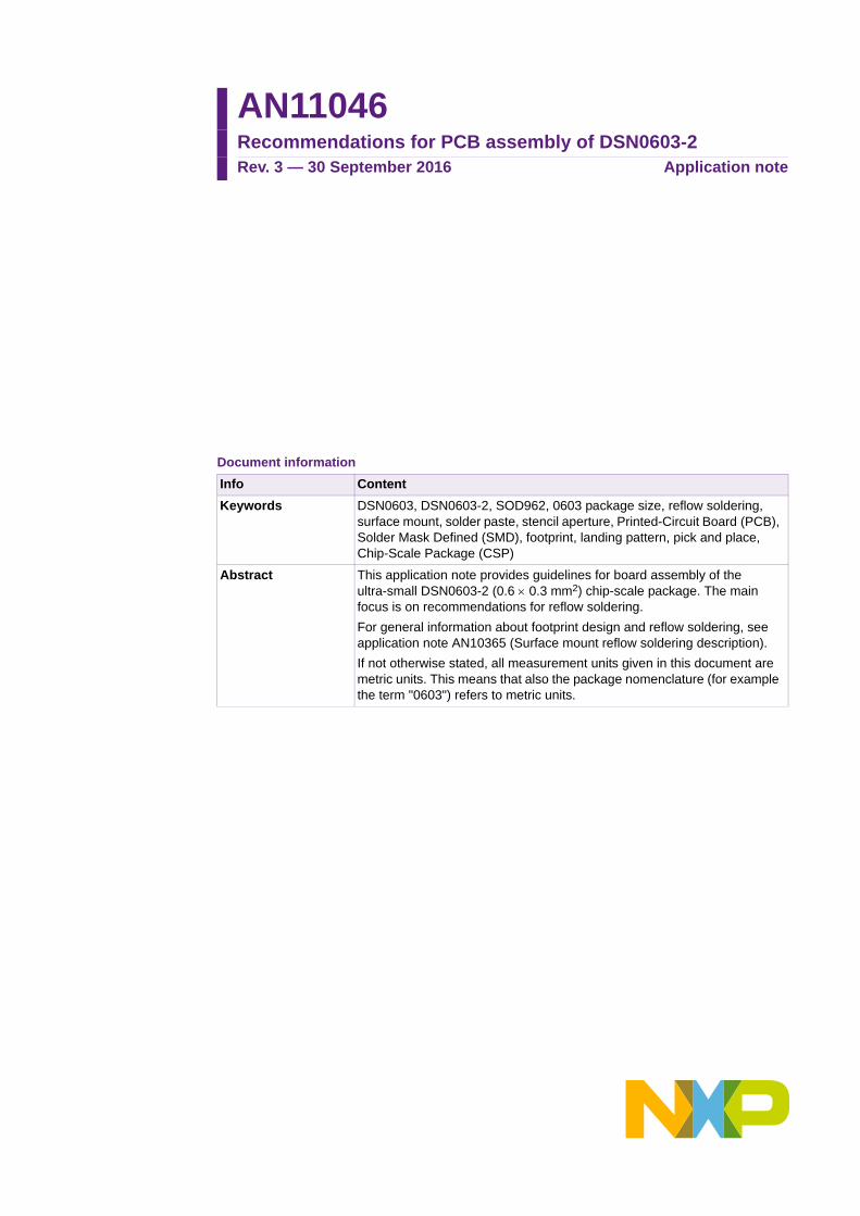
2. DSN0603-2 (SOD962): package details
DSN0603-2 (SOD962) is a Discrete Silicon No-leads (DSN) package. It features either electro-plated copper-tin (CuSn) contacts (CuSn pillars) or electroless plated nickel-palladium-gold (NiPdAu) contacts (pads) under the package (bottom terminations) similar to Discrete Flat No-leads (DFN) style packages. The DSN-style package allows 100 % utilization of the package area for active silicon, offering a significant performance advantage per board area compared to products in plastic-molded packages.
Key Features:
• Ultra small and flat package (0.6 0.3 0.3 mm3)
• 400 m pad pitch
• Pad size 240 240 m2
The visual appearance of DSN0603-2 (SOD962) is shown in Figure 1 whereas Figure 2 shows the package dimensions.
AN11046 All information provided in this document is subject to legal disclaimers. © NXP Semiconductors N.V. 2016. All rights reserved.
Application note Rev. 3 — 30 September 2016 3 of 17
NXP Semiconductors AN11046Recommendations for PCB assembly of DSN0603-2
Fig 1. DSN0603-2 (SOD962): visual appearance
Fig 2. DSN0603-2 (SOD962): package dimensions
ReferencesOutlineversion
Europeanprojection Issue date
IEC JEDEC JEITA
SOD962-2
sod962-2_po
13-07-1213-07-17
Unit
mmmaxnommin
0.32
0.28
0.03 0.325
0.275
0.625
0.5750.4
0.15
0.13
A
Dimensions (mm are the original dimensions)
Note1. The marking bar indicates the cathode.
Leadless ultra small package; 2 terminals; body 0.6 x 0.3 x 0.3 mm SOD962-2
A1 b
0.25
0.23
D E e1 L
0 0.5 mm
scale
A
A1
E
D
(1)
e1
L
b1 2
AN11046 All information provided in this document is subject to legal disclaimers. © NXP Semiconductors N.V. 2016. All rights reserved.
Application note Rev. 3 — 30 September 2016 4 of 17

NXP Semiconductors AN11046Recommendations for PCB assembly of DSN0603-2
3. PCB solder pattern
3.1 Solder pad design: general options
There are two types of solder pad / solder resist designs:
Solder Mask Defined (SMD) and Non-Solder Mask Defined (NSMD).
SMD is a method of designing the solder resist to partially overlap the copper (Cu) landing pattern on the PCB. NSMD designs have a gap between the solder resist and the Cu landing pattern on the PCB. These two types are described in more detail in the next chapter.
3.1.1 SMD solder pad versus NSMD solder pad
If the solder mask extends onto the solder lands, the remaining solderable area is Solder Mask Defined (SMD). The effective solder pad is equal to the copper area that is not covered by the solder mask. This situation is illustrated in Figure 3, left column. In case of an SMD pad, the copper will normally extend 75 m down to 50 m underneath the solder mask on all sides. In other words, the copper dimension is 0.1 mm to 0.15 mm larger than the solder mask dimension. These values may vary depending on the class of PCBs used. This allows tolerances in copper etching and solder mask placement during PCB production.
If the solder mask layer starts outside of the solder lands, and does not cover the copper, this is referred to as Non-Solder Mask Defined (NSMD). The effective solder pad is equal to the copper area. In case of an NSMD, the solder mask should be at least 50 m away from the solder land on all sides. In other words, the solder mask dimension is 100 m larger than the copper dimension. These values may vary depending on the class of PCBs used. The main requirement is that the solder mask is sufficiently far away from the copper, such that - with the given tolerances in solder mask application - it does not extend onto the copper. An NSMD footprint is shown in Figure 3, right column.
a. SMD solder pad b. NSMD solder pad
Fig 3. Solder Mask Defined (SMD) versus Non-Solder Mask Defined (NSMD) solder pads
001aac831 001aac832
AN11046 All information provided in this document is subject to legal disclaimers. © NXP Semiconductors N.V. 2016. All rights reserved.
Application note Rev. 3 — 30 September 2016 5 of 17

NXP Semiconductors AN11046Recommendations for PCB assembly of DSN0603-2
3.2 Solder pad design for DSN0603-2 packages (SOD962)
3.2.1 Recommended reflow solder footprint
Based on the small dimensions of 0603 (0201) devices and the given tolerances for PCB manufacturing, it is recommended to use Non-Solder Mask Defined (NSMD) solder pads.
The DSN0603-2 (SOD962) solder footprint with dimensions and the solder footprint together with the package outline are shown in Figure 4 and Figure 5.
Fig 4. DSN0603-2 (SOD962): recommended reflow solder footprint
Fig 5. DSN0603-2 (SOD962): recommended reflow solder footprint with package outline
aaa-019352
0.2 mm 0.2 mm 0.2 mm
0.28mm
aaa-019353
0.24mm
0.14 mm
0.4 mm
Device
Device pad
Cu pad on PCB
AN11046 All information provided in this document is subject to legal disclaimers. © NXP Semiconductors N.V. 2016. All rights reserved.
Application note Rev. 3 — 30 September 2016 6 of 17
NXP Semiconductors AN11046Recommendations for PCB assembly of DSN0603-2
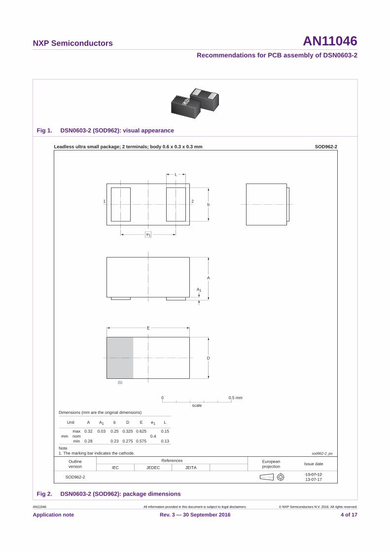
3.2.2 Solder Mask Defined (SMD) footprint on PCB (not recommended)
In case that an SMD solder pad structure is absolutely needed, the recommended solder footprints are given in Figure 6.
As mentioned above, due to the tolerances in the PCB manufacturing, an SMD solder pad structure is not the recommended solution.
Fig 6. Solder Mask Defined (SMD) footprint on PCB
aaa-019354
0.7 mm
0.2 mm 0.2 mm 0.2 mm
0.28mm
Device
Device pad
Cu lines on PCB
Solder mask opening
AN11046 All information provided in this document is subject to legal disclaimers. © NXP Semiconductors N.V. 2016. All rights reserved.
Application note Rev. 3 — 30 September 2016 7 of 17

NXP Semiconductors AN11046Recommendations for PCB assembly of DSN0603-2
4. Solder stencil
4.1 Stencil recommendations
Due to small apertures and pad dimensions, use a high-quality stainless-steel stencil manufactured by laser-cut and with electropolish or plasma coating.
The recommended stencil thickness is 100 m or thinner for the DSN0603-2 package.
For the DSN0603-2 (SOD962) recommended NXP footprint (see Section 3.2.1, Figure 4 and Figure 5), the optimum stencil aperture is shown in Figure 7.
Figure 8 shows the stencil opening in combination with the recommended NXP footprint and the device pad area. Figure 9 shows the stencil and solder mask opening in case of a Solder Mask Defined (SMD) PCB footprint which is not the recommended footprint solution (see Section 3.2.2).
Fig 7. Recommended stencil aperture for DSN0603-2 (SOD962)
aaa-019355
0.256 mm 0.16 mm 0.256 mm
0.256mm
AN11046 All information provided in this document is subject to legal disclaimers. © NXP Semiconductors N.V. 2016. All rights reserved.
Application note Rev. 3 — 30 September 2016 8 of 17

NXP Semiconductors AN11046Recommendations for PCB assembly of DSN0603-2
Fig 8. Stencil opening in combination with Cu pads on PCB and the device pads
aaa-019356
Device pad
Cu pad on PCB
0.256 mm 0.16 mm 0.256 mm
0.256mm
0.28mm
0.2 mm 0.2 mm 0.2 mm
Stencil opening
AN11046 All information provided in this document is subject to legal disclaimers. © NXP Semiconductors N.V. 2016. All rights reserved.
Application note Rev. 3 — 30 September 2016 9 of 17

NXP Semiconductors AN11046Recommendations for PCB assembly of DSN0603-2
SMD footprint on PCB is not the recommended solution
Fig 9. Stencil and solder mask opening in case of an SMD footprint on PCB
aaa-019357
0.7 mm
0.2 mm 0.2 mm 0.2 mm
0.28mm
Device pad Cu lines on PCB
Solder mask opening
0.256mm
Stencil opening
AN11046 All information provided in this document is subject to legal disclaimers. © NXP Semiconductors N.V. 2016. All rights reserved.
Application note Rev. 3 — 30 September 2016 10 of 17
NXP Semiconductors AN11046Recommendations for PCB assembly of DSN0603-2
4.2 Stencil aperture design
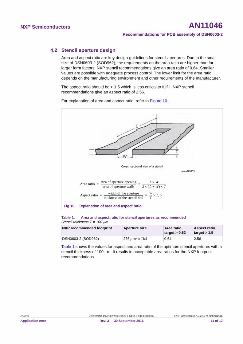
Area and aspect ratio are key design-guidelines for stencil apertures. Due to the small size of DSN0603-2 (SOD962), the requirements on the area ratio are higher than for larger form factors. NXP stencil recommendations give an area ratio of 0.64. Smaller values are possible with adequate process control. The lower limit for the area ratio depends on the manufacturing environment and other requirements of the manufacturer.
The aspect ratio should be > 1.5 which is less critical to fulfill. NXP stencil recommendations give an aspect ratio of 2.56.
For explanation of area and aspect ratio, refer to Figure 10.
Table 1 shows the values for aspect and area ratio of the optimum stencil apertures with a stencil thickness of 100 m. It results in acceptable area ratios for the NXP footprint recommendations.
Fig 10. Explanation of area and aspect ratio
Table 1. Area and aspect ratio for stencil apertures as recommendedStencil thickness T = 100 m
NXP recommended footprint Aperture size Area ratio target > 0.62
Aspect ratio target > 1.5
DSN0603-2 (SOD962) 256 m2 /4 0.64 2.56
Cross -sectional view of a stencilaaa-019083
Area ratio area of aperture openingarea of aperture walls
---------------------------------------------------------- L W2 L W+ T--------------------------------------= =
Aspect ratio width of the aperturethickness of the stencil foil----------------------------------------------------------------
WT----- 1 5= =
AN11046 All information provided in this document is subject to legal disclaimers. © NXP Semiconductors N.V. 2016. All rights reserved.
Application note Rev. 3 — 30 September 2016 11 of 17
NXP Semiconductors AN11046Recommendations for PCB assembly of DSN0603-2
5. Solder paste
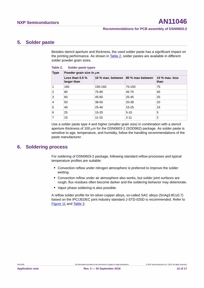
Besides stencil aperture and thickness, the used solder paste has a significant impact on the printing performance. As shown in Table 2, solder pastes are available in different solder powder grain sizes.
Use a solder paste type 4 and higher (smaller grain size) in combination with a stencil aperture thickness of 100 m for the DSN0603-2 (SOD962) package. As solder paste is sensitive to age, temperature, and humidity, follow the handling recommendations of the paste manufacturer.
6. Soldering process
For soldering of DSN0603-2 package, following standard reflow processes and typical temperature profiles are suitable:
• Convection reflow under nitrogen atmosphere is preferred to improve the solder wetting.
• Convection reflow under air atmosphere also works, but solder joint surfaces are rough, flux residues often become darker and the soldering behavior may deteriorate.
• Vapor phase soldering is also possible.
A reflow solder profile for tin-silver-copper alloys, so-called SAC alloys (SnAg3.8Cu0.7) based on the IPC/JEDEC joint industry standard J-STD-020D is recommended. Refer to Figure 11 and Table 3.
Table 2. Solder paste types
Type Powder grain size in m
Less than 0.5 % larger than
10 % max. between 80 % max between 10 % max. less than
1 160 150-160 75-150 75
2 80 75-80 45-75 45
3 60 45-60 25-45 25
4 50 38-50 20-38 20
5 40 25-40 15-25 15
6 25 15-25 5-15 5
7 15 11-15 2-11 2
AN11046 All information provided in this document is subject to legal disclaimers. © NXP Semiconductors N.V. 2016. All rights reserved.
Application note Rev. 3 — 30 September 2016 12 of 17

NXP Semiconductors AN11046Recommendations for PCB assembly of DSN0603-2
7. Handling recommendations
Besides the PCB and stencil design requirements, the ultra small size of the DSN0603 and as consequence the low weight of the component requires that some attention be paid to the pick and place (P&P) process. Electrostatic charge may cause problems during the pick and place (tape out) process. NXP has implemented preventive measures such as using a conductive plastic carrier tape (embossed tape).
For rework, use equipment suitable for the ultra small package size and for handling bare silicon devices. Manual handling with tweezers (e.g. for repair) is not recommended.
Fig 11. Reflow solder profile based on IPC/JEDEC J-STD-020D
Table 3. Pb-free profile feature and specification based on IPC/JEDEC J-STD-020D
Profile feature Values for Pb-free assembly
Average ramp-up rate (Tsmax to Tp) 3 C/s maximum
Preheat
Minimum temperature (Tsmin) 150 C
Maximum temperature (Tsmax) 200 C
Time (ts) from Tsmin to Tsmax 60 s to 180 s
Liquidus temperature (TL) 217 C
Time (tL) maintained above TL 60 s to 150 s
Peak/classification temperature (Tp) 260 C
Time within 5 C of actual peak temperature (tp) 10 s to 30 s
Ramp-down rate 6 C/s maximum
Time 25 C to peak temperature (t25°C to peak) 8 minutes maximum
aaa-019084
ramp-down
timeT25 °C to peak
tspreheat
25 °C
TLTsmax
Tsmin
Tp
temperature
ramp-up
tp
tL
critical zoneTL to Tp
AN11046 All information provided in this document is subject to legal disclaimers. © NXP Semiconductors N.V. 2016. All rights reserved.
Application note Rev. 3 — 30 September 2016 13 of 17
NXP Semiconductors AN11046Recommendations for PCB assembly of DSN0603-2
8. Summary
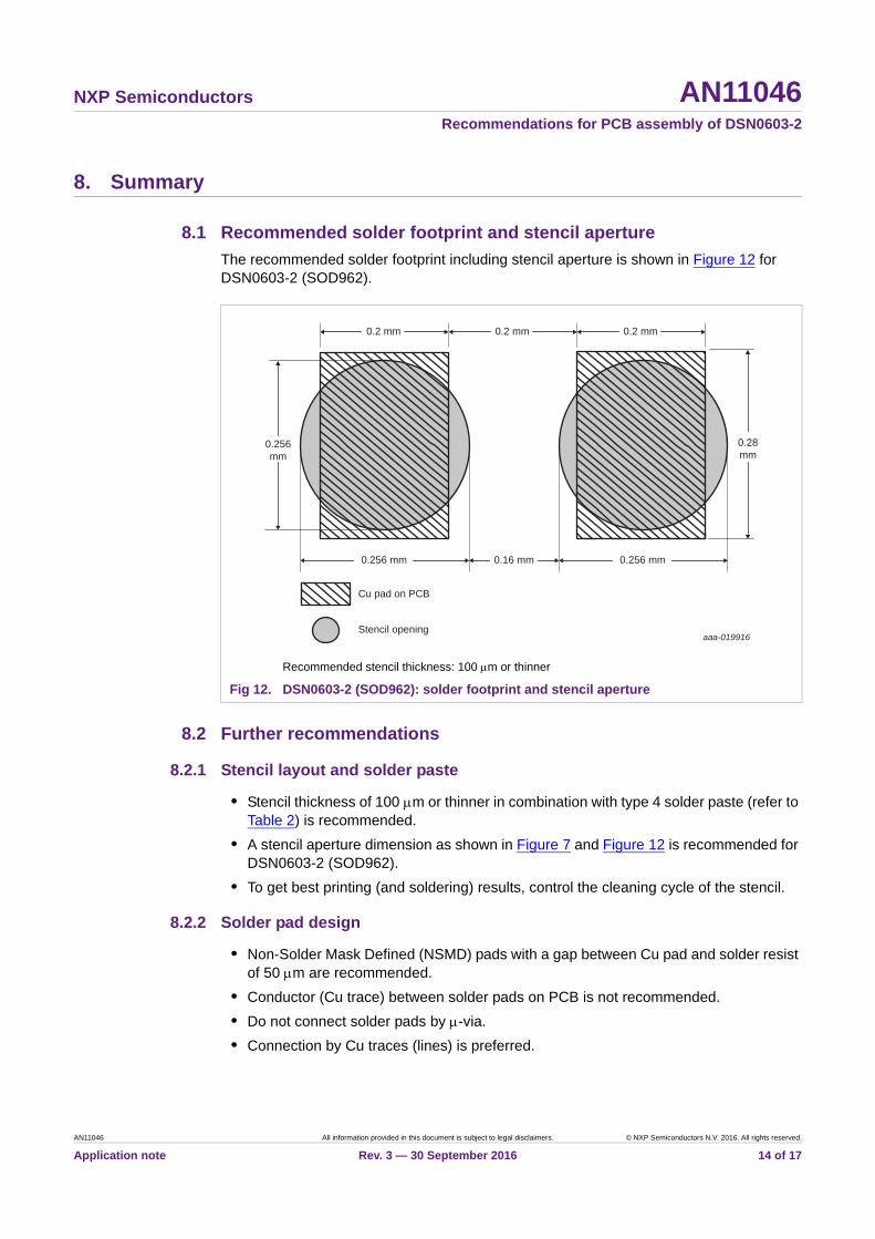
8.1 Recommended solder footprint and stencil aperture
The recommended solder footprint including stencil aperture is shown in Figure 12 for DSN0603-2 (SOD962).
8.2 Further recommendations
8.2.1 Stencil layout and solder paste
• Stencil thickness of 100 m or thinner in combination with type 4 solder paste (refer to Table 2) is recommended.
• A stencil aperture dimension as shown in Figure 7 and Figure 12 is recommended for DSN0603-2 (SOD962).
• To get best printing (and soldering) results, control the cleaning cycle of the stencil.
8.2.2 Solder pad design
• Non-Solder Mask Defined (NSMD) pads with a gap between Cu pad and solder resist of 50 m are recommended.
• Conductor (Cu trace) between solder pads on PCB is not recommended.
• Do not connect solder pads by -via.
• Connection by Cu traces (lines) is preferred.
Recommended stencil thickness: 100 m or thinner
Fig 12. DSN0603-2 (SOD962): solder footprint and stencil aperture
aaa-019916
Cu pad on PCB
0.256 mm 0.16 mm 0.256 mm
0.256mm
0.28mm
0.2 mm 0.2 mm 0.2 mm
Stencil opening
AN11046 All information provided in this document is subject to legal disclaimers. © NXP Semiconductors N.V. 2016. All rights reserved.
Application note Rev. 3 — 30 September 2016 14 of 17
NXP Semiconductors AN11046Recommendations for PCB assembly of DSN0603-2
8.2.3 Soldering process
• Convection reflow under nitrogen atmosphere is preferred.
• Convection reflow under air atmosphere also works, but:
– Using an unfavorable layout, products lean toward undefined tilting and rotation and solder joints tend to more voiding.
– Solder joint surfaces are rough, flux residues often become darker and the soldering behavior may deteriorate.
• Vapor phase soldering is also possible.
8.2.4 Handling recommendations
• Manual handling with tweezers (e.g. for repair) is not recommended.
• Keep control of thawing time of solder paste bundle to avoid too much humidity in paste.
• To prevent drying of flux in solder paste, maintain the relative humidity of shop floor at solder paste print until reflow to 40 % to 60 %.
• Relative humidity of shop floor at pick and place > 30 %.
AN11046 All information provided in this document is subject to legal disclaimers. © NXP Semiconductors N.V. 2016. All rights reserved.
Application note Rev. 3 — 30 September 2016 15 of 17

NXP Semiconductors AN11046Recommendations for PCB assembly of DSN0603-2
9. Legal information
9.1 Definitions
Draft — The document is a draft version only. The content is still under internal review and subject to formal approval, which may result in modifications or additions. NXP Semiconductors does not give any representations or warranties as to the accuracy or completeness of information included herein and shall have no liability for the consequences of use of such information.
9.2 Disclaimers
Limited warranty and liability — Information in this document is believed to be accurate and reliable. However, NXP Semiconductors does not give any representations or warranties, expressed or implied, as to the accuracy or completeness of such information and shall have no liability for the consequences of use of such information. NXP Semiconductors takes no responsibility for the content in this document if provided by an information source outside of NXP Semiconductors.
In no event shall NXP Semiconductors be liable for any indirect, incidental, punitive, special or consequential damages (including - without limitation - lost profits, lost savings, business interruption, costs related to the removal or replacement of any products or rework charges) whether or not such damages are based on tort (including negligence), warranty, breach of contract or any other legal theory.
Notwithstanding any damages that customer might incur for any reason whatsoever, NXP Semiconductors’ aggregate and cumulative liability towards customer for the products described herein shall be limited in accordance with the Terms and conditions of commercial sale of NXP Semiconductors.
Right to make changes — NXP Semiconductors reserves the right to make changes to information published in this document, including without limitation specifications and product descriptions, at any time and without notice. This document supersedes and replaces all information supplied prior to the publication hereof.
Suitability for use — NXP Semiconductors products are not designed, authorized or warranted to be suitable for use in life support, life-critical or safety-critical systems or equipment, nor in applications where failure or malfunction of an NXP Semiconductors product can reasonably be expected to result in personal injury, death or severe property or environmental damage. NXP Semiconductors and its suppliers accept no liability for inclusion and/or use of NXP Semiconductors products in such equipment or applications and therefore such inclusion and/or use is at the customer’s own risk.
Applications — Applications that are described herein for any of these products are for illustrative purposes only. NXP Semiconductors makes no representation or warranty that such applications will be suitable for the specified use without further testing or modification.
Customers are responsible for the design and operation of their applications and products using NXP Semiconductors products, and NXP Semiconductors accepts no liability for any assistance with applications or customer product
design. It is customer’s sole responsibility to determine whether the NXP Semiconductors product is suitable and fit for the customer’s applications and products planned, as well as for the planned application and use of customer’s third party customer(s). Customers should provide appropriate design and operating safeguards to minimize the risks associated with their applications and products.
NXP Semiconductors does not accept any liability related to any default, damage, costs or problem which is based on any weakness or default in the customer’s applications or products, or the application or use by customer’s third party customer(s). Customer is responsible for doing all necessary testing for the customer’s applications and products using NXP Semiconductors products in order to avoid a default of the applications and the products or of the application or use by customer’s third party customer(s). NXP does not accept any liability in this respect.
Export control — This document as well as the item(s) described herein may be subject to export control regulations. Export might require a prior authorization from competent authorities.
Evaluation products — This product is provided on an “as is” and “with all faults” basis for evaluation purposes only. NXP Semiconductors, its affiliates and their suppliers expressly disclaim all warranties, whether express, implied or statutory, including but not limited to the implied warranties of non-infringement, merchantability and fitness for a particular purpose. The entire risk as to the quality, or arising out of the use or performance, of this product remains with customer.
In no event shall NXP Semiconductors, its affiliates or their suppliers be liable to customer for any special, indirect, consequential, punitive or incidental damages (including without limitation damages for loss of business, business interruption, loss of use, loss of data or information, and the like) arising out the use of or inability to use the product, whether or not based on tort (including negligence), strict liability, breach of contract, breach of warranty or any other theory, even if advised of the possibility of such damages.
Notwithstanding any damages that customer might incur for any reason whatsoever (including without limitation, all damages referenced above and all direct or general damages), the entire liability of NXP Semiconductors, its affiliates and their suppliers and customer’s exclusive remedy for all of the foregoing shall be limited to actual damages incurred by customer based on reasonable reliance up to the greater of the amount actually paid by customer for the product or five dollars (US$5.00). The foregoing limitations, exclusions and disclaimers shall apply to the maximum extent permitted by applicable law, even if any remedy fails of its essential purpose.
Translations — A non-English (translated) version of a document is for reference only. The English version shall prevail in case of any discrepancy between the translated and English versions.
9.3 TrademarksNotice: All referenced brands, product names, service names and trademarks are the property of their respective owners.
AN11046 All information provided in this document is subject to legal disclaimers. © NXP Semiconductors N.V. 2016. All rights reserved.
Application note Rev. 3 — 30 September 2016 16 of 17
NXP Semiconductors AN11046Recommendations for PCB assembly of DSN0603-2
10. Contents
1 Introduction . . . . . . . . . . . . . . . . . . . . . . . . . . . . 3
2 DSN0603-2 (SOD962): package details . . . . . . 3
3 PCB solder pattern . . . . . . . . . . . . . . . . . . . . . . 53.1 Solder pad design: general options . . . . . . . . . 53.1.1 SMD solder pad versus NSMD solder pad . . . . 53.2 Solder pad design for DSN0603-2 packages
(SOD962) . . . . . . . . . . . . . . . . . . . . . . . . . . . . . 63.2.1 Recommended reflow solder footprint . . . . . . . 63.2.2 Solder Mask Defined (SMD) footprint on PCB (not
recommended) . . . . . . . . . . . . . . . . . . . . . . . . . 7
4 Solder stencil . . . . . . . . . . . . . . . . . . . . . . . . . . . 84.1 Stencil recommendations . . . . . . . . . . . . . . . . . 84.2 Stencil aperture design . . . . . . . . . . . . . . . . . . 11
5 Solder paste . . . . . . . . . . . . . . . . . . . . . . . . . . . 12
6 Soldering process . . . . . . . . . . . . . . . . . . . . . . 12
7 Handling recommendations . . . . . . . . . . . . . . 13
8 Summary . . . . . . . . . . . . . . . . . . . . . . . . . . . . . 148.1 Recommended solder footprint and stencil
aperture . . . . . . . . . . . . . . . . . . . . . . . . . . . . . 148.2 Further recommendations . . . . . . . . . . . . . . . 148.2.1 Stencil layout and solder paste. . . . . . . . . . . . 148.2.2 Solder pad design. . . . . . . . . . . . . . . . . . . . . . 148.2.3 Soldering process. . . . . . . . . . . . . . . . . . . . . . 158.2.4 Handling recommendations . . . . . . . . . . . . . . 15
9 Legal information. . . . . . . . . . . . . . . . . . . . . . . 169.1 Definitions. . . . . . . . . . . . . . . . . . . . . . . . . . . . 169.2 Disclaimers . . . . . . . . . . . . . . . . . . . . . . . . . . . 169.3 Trademarks. . . . . . . . . . . . . . . . . . . . . . . . . . . 16
10 Contents . . . . . . . . . . . . . . . . . . . . . . . . . . . . . . 17
© NXP Semiconductors N.V. 2016. All rights reserved.
For more information, please visit: http://www.nxp.comFor sales office addresses, please send an email to: [email protected]
Date of release: 30 September 2016
Document identifier: AN11046
Please be aware that important notices concerning this document and the product(s)described herein, have been included in section ‘Legal information’.