Embed Size (px)
Citation preview
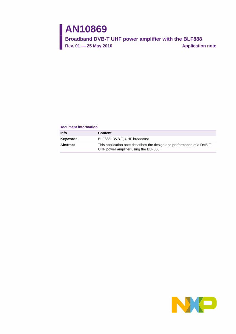
AN10869Broadband DVB-T UHF power amplifier with the BLF888Rev. 01 — 25 May 2010 Application note
Document informationInfo ContentKeywords BLF888, DVB-T, UHF broadcast
Abstract This application note describes the design and performance of a DVB-T UHF power amplifier using the BLF888.
NXP Semiconductors AN10869Broadband DVB-T UHF power amplifier with the BLF888
Revision historyRev Date Description
01 20100525 Initial version
AN10869_1 All information provided in this document is subject to legal disclaimers. © NXP B.V. 2010. All rights reserved.
Application note Rev. 01 — 25 May 2010 2 of 21

NXP Semiconductors AN10869Broadband DVB-T UHF power amplifier with the BLF888
1. Introduction
For the past few years, new product design in the broadcast industry has been dominated by emerging digital modulation standards. A specific example is broadcast television, where many new transmitter systems are currently being set up as part of the conversion to digital terrestrial television.
The BLF888 is a UHF LDMOS power transistor intended for the broadcast transmitter market. It can deliver 110 W DVB-T average power over the full UHF band from 470 MHz to 860 MHz at a CCDF of 8 dB (0.01 %). The transistor is also capable of handling analog TV (ATV) signals. The average power delivered will be dependent on cooling conditions.
Today, UHF transmitter design focuses on increasing efficiency and output power, while reducing size. To achieve these goals, the next generation of UHF transistors must deliver greater power levels, increased efficiency and higher gain, and the size of application boards needs to be reduced. The BLF888 meets these requirements.
This report describes a broadband application incorporating the BLF888, built on a small form factor board with a total size of 105 mm × 50 mm.
2. Circuit description
The BLF888 broadband application circuit is shown in Figure 1. It is a Class AB common source amplifier. Circuit dimensions are 105 mm × 50 mm (including the transistor). If the connectors are excluded, the dimensions are 95 mm × 50 mm. The PCB material is Taconic RF35 (εr = 3.5) with a thickness of 0.76 mm.
Fig 1. BLF888 broadband application circuit
014aab143
AN10869_1 All information provided in this document is subject to legal disclaimers. © NXP B.V. 2010. All rights reserved.
Application note Rev. 01 — 25 May 2010 3 of 21
xxxxxxxxxxxxxxxxxxxxx xxxxxxxxxxxxxxxxxxxxxxxxxx xxxxxxx x x x xxxxxxxxxxxxxxxxxxxxxxxxxxxxxx xxxxxxxxxxxxxxxxxxx xx xx xxxxx xxxxxxxxxxxxxxxxxxxxxxxxxxx xxxxxxxxxxxxxxxxxxx xxxxxx xxxxxxxxxxxxxxxxxxxxxxxxxxxxxxxxxxx xxxxxxxxxxxx x x xxxxxxxxxxxxxxxxxxxxx xxxxxxxxxxxxxxxxxxxxxxxxxxxxxx xxxxx xxxxxxxxxxxxxxxxxxxxxxxxxxxxxxxxxxxxxxxxxxxxxxxxxx xxxxxxxx xxxxxxxxxxxxxxxxxxxxxxxxx xxxxxxxxxxxxxxxxxxxx xxx
AN10869_1
Application note
NXP Sem
iconductorsA
N10869
Broadband D
VB-T U
HF pow
er amplifier w
ith the BLF888
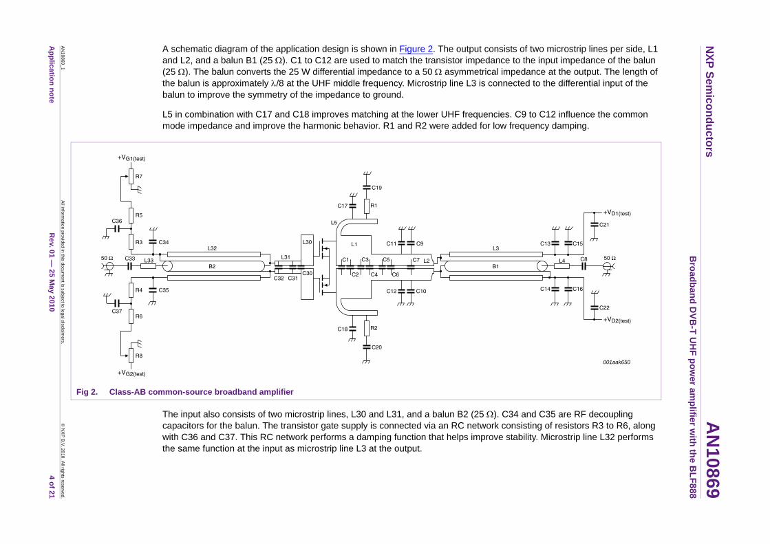
A schematic diagram of the application design is shown in Figure 2. The output consists of two microstrip lines per side, L1 and L2, and a balun B1 (25 Ω). C1 to C12 are used to match the transistor impedance to the input impedance of the balun (25 Ω). The balun converts the 25 W differential impedance to a 50 Ω asymmetrical impedance at the output. The length of the balun is approximately λ/8 at the UHF middle frequency. Microstrip line L3 is connected to the differential input of the balun to improve the symmetry of the impedance to ground.
. C9 to C12 influence the common frequency damping.
34 and C35 are RF decoupling nsisting of resistors R3 to R6, along tability. Microstrip line L32 performs
001aak650
+VD1(test)
+VD2(test)
C15
C8 50 ΩL4
C21
C22
C13
C16C14
All information provided in this docum
ent is subject to legal disclaimers.
© N
XP B.V. 2010. All rights reserved.
Rev. 01 —
25 May 2010
4 of 21
L5 in combination with C17 and C18 improves matching at the lower UHF frequenciesmode impedance and improve the harmonic behavior. R1 and R2 were added for low
The input also consists of two microstrip lines, L30 and L31, and a balun B2 (25 Ω). Ccapacitors for the balun. The transistor gate supply is connected via an RC network cowith C36 and C37. This RC network performs a damping function that helps improve sthe same function at the input as microstrip line L3 at the output.
Fig 2. Class-AB common-source broadband amplifier
+VG1(test)
R7
R5
R3 C34
C33 L33
C32 C31C30
C19
C20
C9
50 Ω C1
C2 C4
C3
C6
C7C5
C11
C10C12
C17
C18
C36
+VG2(test)
R8
R6
R4 C35
C37
L32L30 L1
L2
R1
R2
L5
L31
B2
L3
B1
NXP Semiconductors AN10869Broadband DVB-T UHF power amplifier with the BLF888
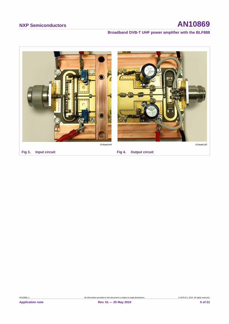
Fig 3. Input circuit Fig 4. Output circuit
014aab144 014aab145
AN10869_1 All information provided in this document is subject to legal disclaimers. © NXP B.V. 2010. All rights reserved.
Application note Rev. 01 — 25 May 2010 5 of 21
NXP Semiconductors AN10869Broadband DVB-T UHF power amplifier with the BLF888
3. Design and Simulation
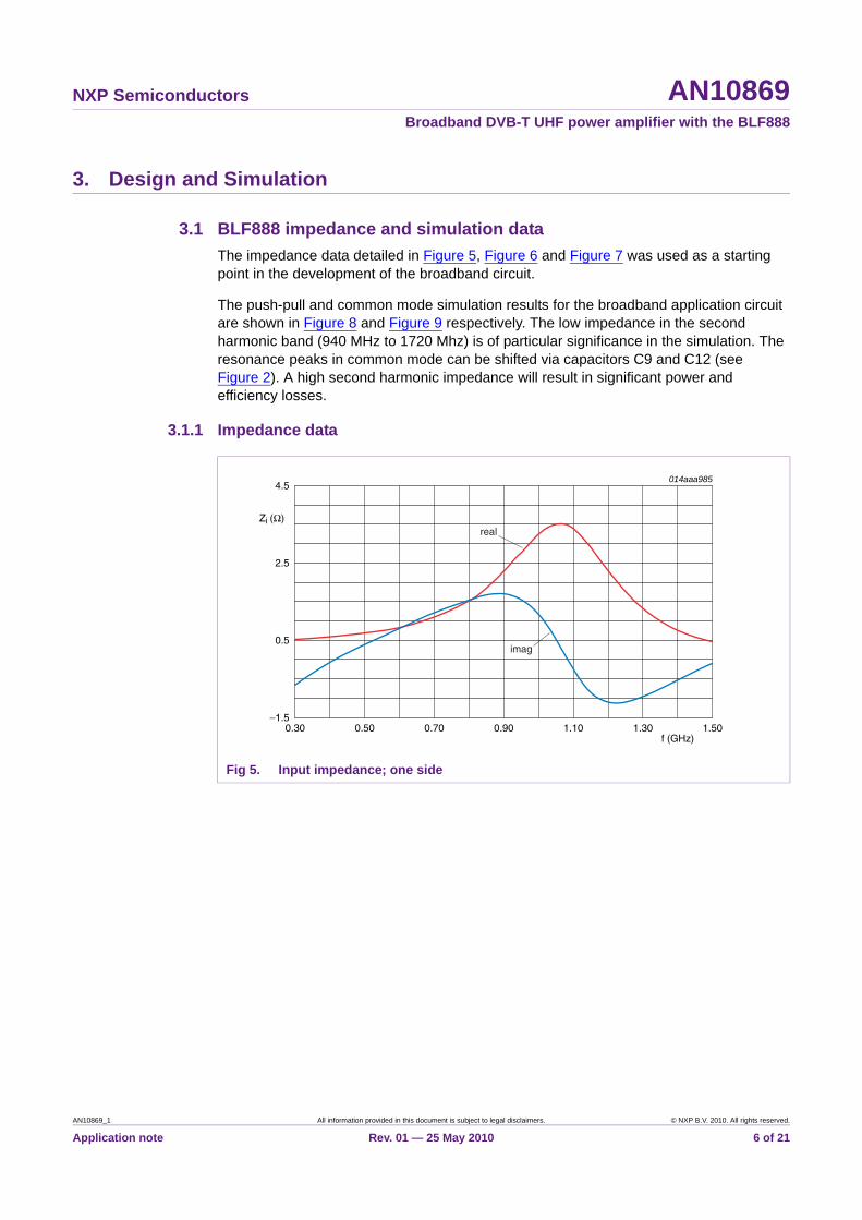
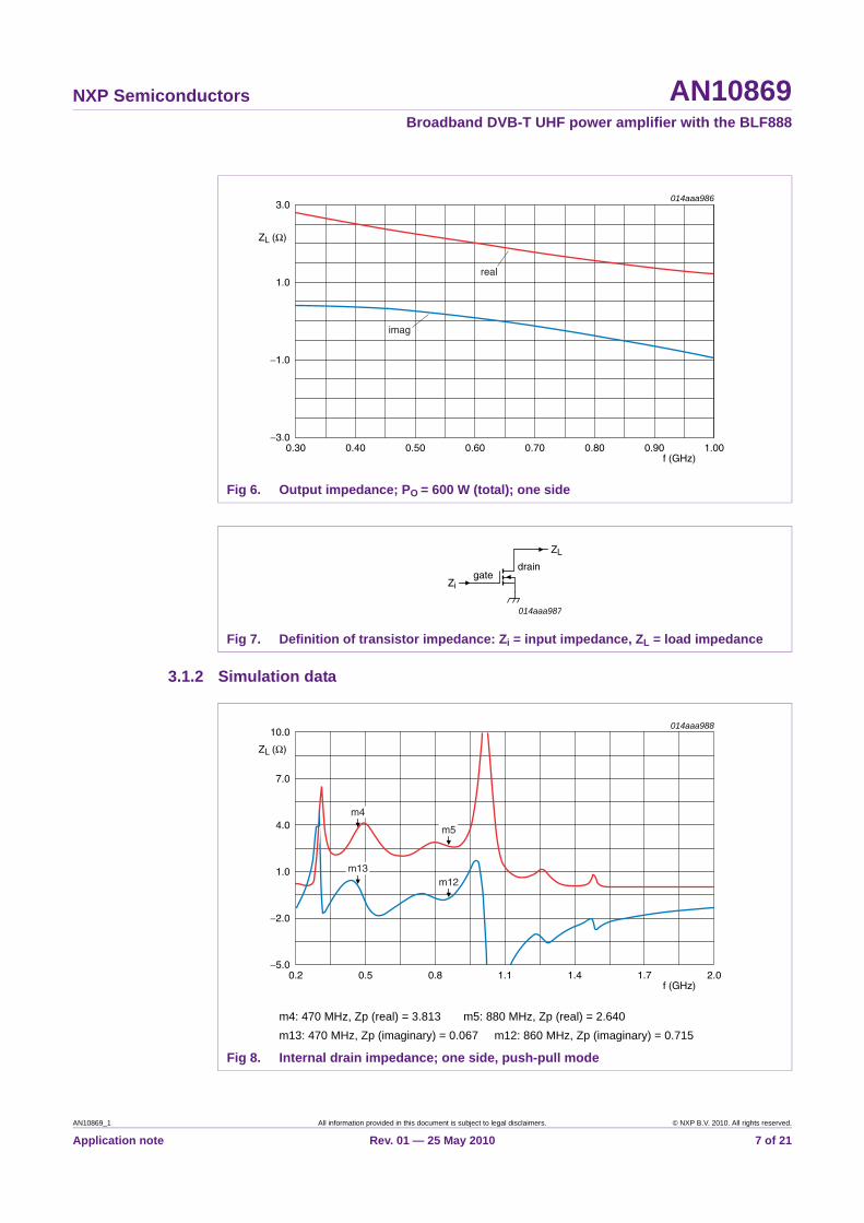
3.1 BLF888 impedance and simulation dataThe impedance data detailed in Figure 5, Figure 6 and Figure 7 was used as a starting point in the development of the broadband circuit.
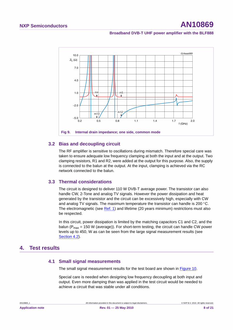
The push-pull and common mode simulation results for the broadband application circuit are shown in Figure 8 and Figure 9 respectively. The low impedance in the second harmonic band (940 MHz to 1720 Mhz) is of particular significance in the simulation. The resonance peaks in common mode can be shifted via capacitors C9 and C12 (see Figure 2). A high second harmonic impedance will result in significant power and efficiency losses.
3.1.1 Impedance data
Fig 5. Input impedance; one side
real
imag
014aaa985
f (GHz)0.30 1.501.100.700.50 1.300.90
0.5
2.5
4.5
Zi (Ω)
−1.5
AN10869_1 All information provided in this document is subject to legal disclaimers. © NXP B.V. 2010. All rights reserved.
Application note Rev. 01 — 25 May 2010 6 of 21
NXP Semiconductors AN10869Broadband DVB-T UHF power amplifier with the BLF888
3.1.2 Simulation data
Fig 6. Output impedance; PO = 600 W (total); one side
Fig 7. Definition of transistor impedance: Zi = input impedance, ZL = load impedance
real
imag
f (GHz)0.30 1.000.800.600.40 0.50 0.900.70
014aaa986
−1.0
1.0
3.0
ZL (Ω)
−3.0
ZL
draingate
Zi
014aaa987
m4: 470 MHz, Zp (real) = 3.813 m5: 880 MHz, Zp (real) = 2.640m13: 470 MHz, Zp (imaginary) = 0.067 m12: 860 MHz, Zp (imaginary) = 0.715
Fig 8. Internal drain impedance; one side, push-pull mode
f (GHz)0.2 2.01.40.8
014aaa988
1.0
4.0
−2.0
7.0
10.0
ZL (Ω)
−5.00.5 1.71.1
m4
m13m12
m5
AN10869_1 All information provided in this document is subject to legal disclaimers. © NXP B.V. 2010. All rights reserved.
Application note Rev. 01 — 25 May 2010 7 of 21
NXP Semiconductors AN10869Broadband DVB-T UHF power amplifier with the BLF888
3.2 Bias and decoupling circuitThe RF amplifier is sensitive to oscillations during mismatch. Therefore special care was taken to ensure adequate low frequency clamping at both the input and at the output. Two clamping resistors, R1 and R2, were added at the output for this purpose. Also, the supply is connected to the balun at the output. At the input, clamping is achieved via the RC network connected to the balun.
3.3 Thermal considerationsThe circuit is designed to deliver 110 W DVB-T average power. The transistor can also handle CW, 2-Tone and analog TV signals. However the power dissipation and heat generated by the transistor and the circuit can be excessively high, especially with CW and analog TV signals. The maximum temperature the transistor can handle is 200 °C. The electromagnetic (see Ref. 1) and lifetime (20 years minimum) restrictions must also be respected.
In this circuit, power dissipation is limited by the matching capacitors C1 and C2, and the balun (Pmax = 150 W (average)). For short-term testing, the circuit can handle CW power levels up to 450, W as can be seen from the large signal measurement results (see Section 4.2).
4. Test results
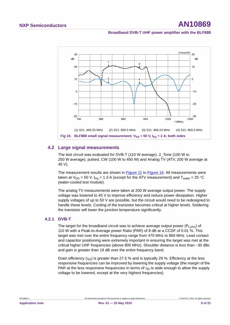
4.1 Small signal measurementsThe small signal measurement results for the test board are shown in Figure 10.
Special care is needed when designing low frequency decoupling at both input and output. Even more damping than was applied in the test circuit would be needed to achieve a circuit that was stable under all conditions.
Fig 9. Internal drain impedance; one side, common mode
f (GHz)0.2 2.01.40.8
014aaa989
1.0
4.0
−2.0
7.0
10.0
ZL (Ω)
−5.00.5 1.71.1
m4 m5
m12m13
AN10869_1 All information provided in this document is subject to legal disclaimers. © NXP B.V. 2010. All rights reserved.
Application note Rev. 01 — 25 May 2010 8 of 21
NXP Semiconductors AN10869Broadband DVB-T UHF power amplifier with the BLF888
4.2 Large signal measurementsThe test circuit was evaluated for DVB-T (110 W average), 2_Tone (100 W to 250 W average), pulsed, CW (100 W to 450 W) and Analog TV (ATV, 200 W average at 45 V).
The measurement results are shown in Figure 11 to Figure 16. All measurements were taken at VDD = 50 V, IDq = 1.3 A (except for the ATV measurement) and Twater = 25 °C (water-cooled test module).
The analog TV measurements were taken at 200 W average output power. The supply voltage was lowered to 45 V to improve efficiency and reduce power dissipation. Higher supply voltages of up to 50 V are possible, but the circuit would need to be redesigned to handle these levels. Cooling of the transistor becomes critical at higher levels. Soldering the transistor will lower the junction temperature significantly.
4.2.1 DVB-TThe target for the broadband circuit was to achieve average output power (PL(AV)) of 110 W with a Peak-to-Average power Ratio (PAR) of 8 dB at a CCDF of 0.01 %. This target was met over the entire frequency range from 470 MHz to 860 MHz. Lead contact and capacitor positioning were extremely important in ensuring the target was met at the critical higher UHF frequencies (above 800 MHz). Shoulder distance is less than −30 dBc and gain is greater than 19 dB over the entire frequency band.
Drain efficiency (ηD) is greater than 27.5 % and is typically 29 %. Efficiency at the less responsive frequencies can be improved by lowering the supply voltage (the margin of the PAR at the less responsive frequencies in terms of ηD is wide enough to allow the supply voltage to be lowered, except at the very highest frequencies).
(1) S21: 469.25 MHz (2) S21: 859.5 MHz (3) S11: 469.23 MHz (4) S11: 859.5 MHz
Fig 10. BLF888 small signal measurement; VDS = 50 V, IDq = 2 A; both sides
f (MHz)100 15001220660 940380
0
10
−10
20
30
dB
−20
−10
0
−20
10
20
dB
−30
2
4
1
3
014aaa990
AN10869_1 All information provided in this document is subject to legal disclaimers. © NXP B.V. 2010. All rights reserved.
Application note Rev. 01 — 25 May 2010 9 of 21

NXP Semiconductors AN10869Broadband DVB-T UHF power amplifier with the BLF888
a. Input spectrum DVB-T 8k; Δf(2-1) = 4.3 MHz (−50 dB)
b. Output spectrum DVB-T 8k with BLF888 @ 714 MHz/110 W (average); Δf(2-1) = 4.3 MHz (−36.5 dB)
Fig 11. BLF888 large signal measurement: DVB-T with PAR of input signal = 9.5 dB at 0.01 % probability on CCDF
MHz848 868864856 860
1
2
852
−40
−60
−20
0
dBm
−80
014aaa991
MHz704 724720712 716708
−40
−60
−20
0
dBm
−80
1
2
014aaa992
AN10869_1 All information provided in this document is subject to legal disclaimers. © NXP B.V. 2010. All rights reserved.
Application note Rev. 01 — 25 May 2010 10 of 21
NXP Semiconductors AN10869Broadband DVB-T UHF power amplifier with the BLF888
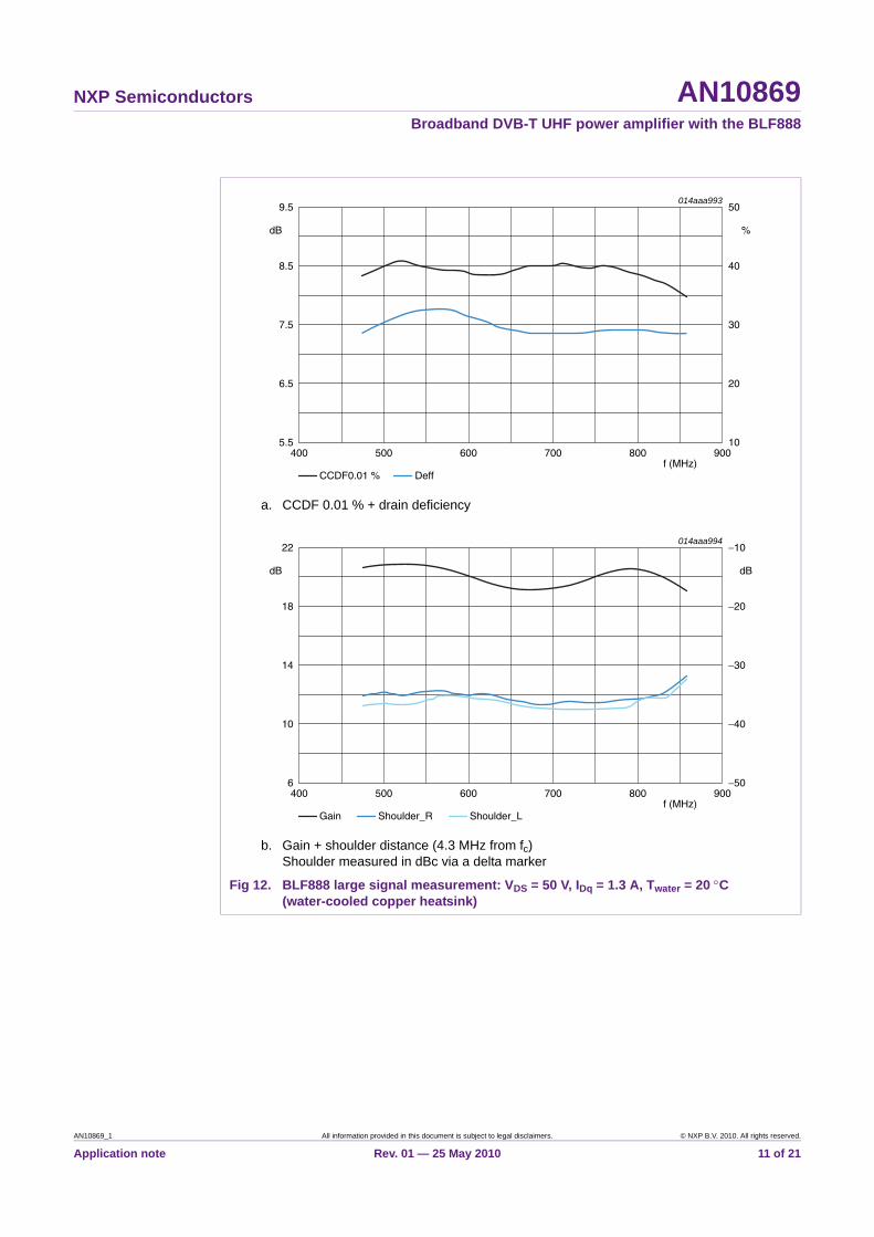
a. CCDF 0.01 % + drain deficiency
b. Gain + shoulder distance (4.3 MHz from fc)Shoulder measured in dBc via a delta marker
Fig 12. BLF888 large signal measurement: VDS = 50 V, IDq = 1.3 A, Twater = 20 °C (water-cooled copper heatsink)
f (MHz)400
CCDF0.01 %
900800600 700500
014aaa993
7.5
6.5
8.5
9.5
dB
5.5
30
20
40
50
%
10
Deff
f (MHz)400
Gain
900800600 700500
014aaa994
14
10
18
22
dB
6
−30
−40
−20
−10
dB
−50
Shoulder_R Shoulder_L
AN10869_1 All information provided in this document is subject to legal disclaimers. © NXP B.V. 2010. All rights reserved.
Application note Rev. 01 — 25 May 2010 11 of 21

NXP Semiconductors AN10869Broadband DVB-T UHF power amplifier with the BLF888
4.2.2 2-toneMeasurements were taken at PL(AV) = 150 W to 250 W (average). IMD3 levels are well below −30 dBc except at the highest frequencies at 500 W PEP. At these power levels, drain efficiency > 40 % over the entire UHF band.
a. 2-tone, gain and drain efficiency
b. 2-tone, gain and IMD3 (max)
Fig 13. BLF888 large signal measurement: 2-tone broadband measurement at different PL(AV) levels (150 W to 250 W); VDS = 50 V, IDq = 1.3 A, Twater = 20 °C (water-cooled heatsink); Δf = 100 kHz, 2 carriers with equal amplitude
f (MHz)400
Gain_150
900800600 700500
014aaa995
16
12
20
24
dB
8
40
30
50
60
%
20
Gain_200Gain_250
Deff_150Deff_200Deff_250
f (MHz)400 900800600 700500
014aaa996
16
12
20
24
dB
8
−35
−45
−25
−15
dB
−55
Gain_150Gain_200Gain_250
IMD3max_150IMD3max_200IMD3max_250
AN10869_1 All information provided in this document is subject to legal disclaimers. © NXP B.V. 2010. All rights reserved.
Application note Rev. 01 — 25 May 2010 12 of 21

NXP Semiconductors AN10869Broadband DVB-T UHF power amplifier with the BLF888
4.2.3 PulsedPulsed measurement results between 470 MHz and 860 MHz (duty cycle = 10 %, tp =100 µs) are shown in Figure 14. This provides a clear illustration of the peak power capability of this circuit. The lowest peak power level (≈550 W) occurs at 860 MHz (which corresponds with the DVB-T results).
Gain + power added efficiency, tp = 100 μs (pulse duration), δ = 10 % (duty cycle),T = 1 ms (period)VDS = 50 V, IDq = 1.3 A, Twater = 20 °C (water-cooled heatsink)
Fig 14. BLF888 large signal measurement: pulsed broadband measurement
Ppeak (W)0 800600200 400
014aaa997
18
20
22
Ga(dB)
16
25
45
65
Eff(%)
5
Gain_860Gain_810Gain_762
Gain_666Gain_618Gain_570
Gain_474Pa_eff_860Pa_eff_810
Gain_714 Gain_522 Pa_eff_762
Pa_eff_714Pa_eff_666Pa_eff_618
Pa_eff_570Pa_eff_522Pa_eff_474
AN10869_1 All information provided in this document is subject to legal disclaimers. © NXP B.V. 2010. All rights reserved.
Application note Rev. 01 — 25 May 2010 13 of 21
NXP Semiconductors AN10869Broadband DVB-T UHF power amplifier with the BLF888
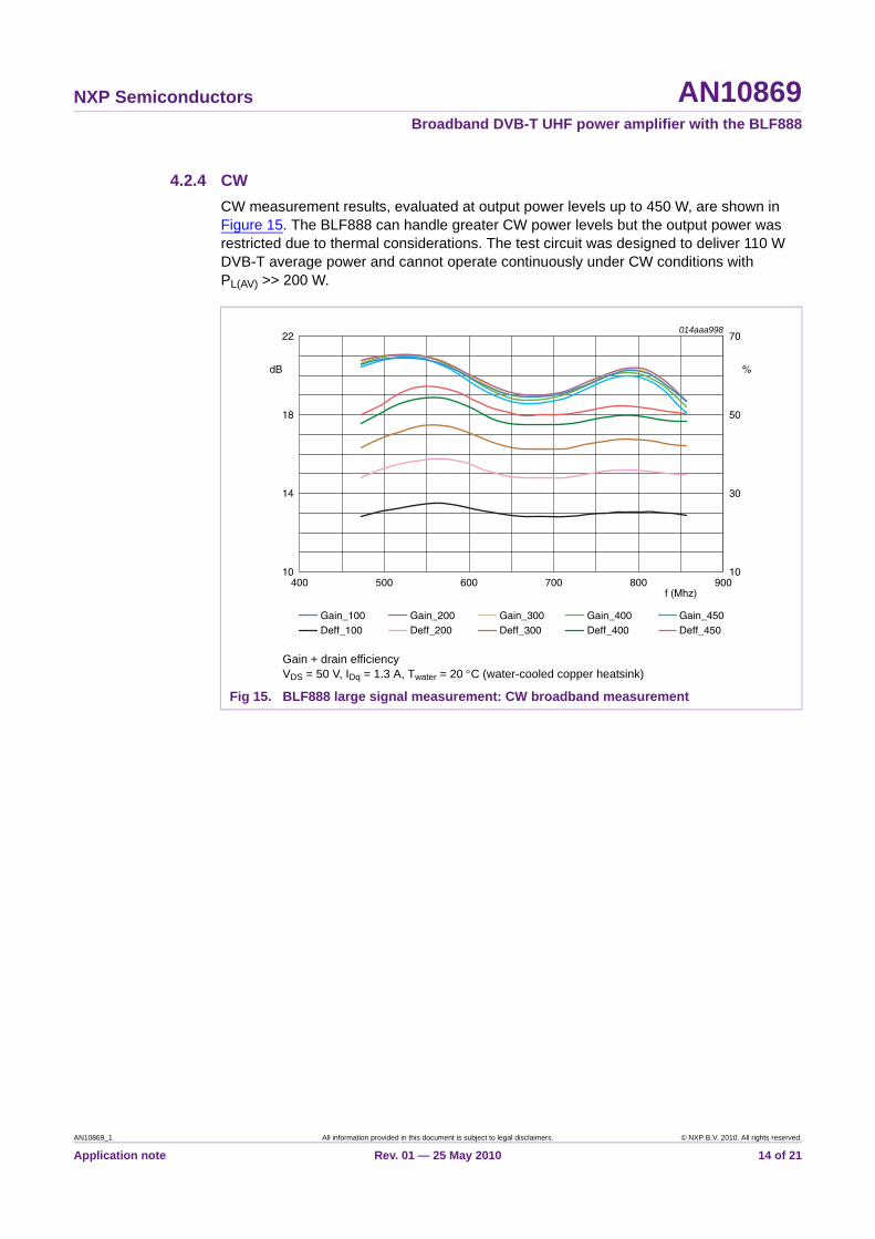
4.2.4 CWCW measurement results, evaluated at output power levels up to 450 W, are shown in Figure 15. The BLF888 can handle greater CW power levels but the output power was restricted due to thermal considerations. The test circuit was designed to deliver 110 W DVB-T average power and cannot operate continuously under CW conditions with PL(AV) >> 200 W.
Gain + drain efficiencyVDS = 50 V, IDq = 1.3 A, Twater = 20 °C (water-cooled copper heatsink)
Fig 15. BLF888 large signal measurement: CW broadband measurement
Gain_100Deff_100
Gain_200Deff_200
Gain_300Deff_300
Gain_400Deff_400
Gain_450Deff_450
f (Mhz)400 900800600 700500
014aaa998
14
18
22
dB
10
30
50
70
%
10
AN10869_1 All information provided in this document is subject to legal disclaimers. © NXP B.V. 2010. All rights reserved.
Application note Rev. 01 — 25 May 2010 14 of 21
NXP Semiconductors AN10869Broadband DVB-T UHF power amplifier with the BLF888
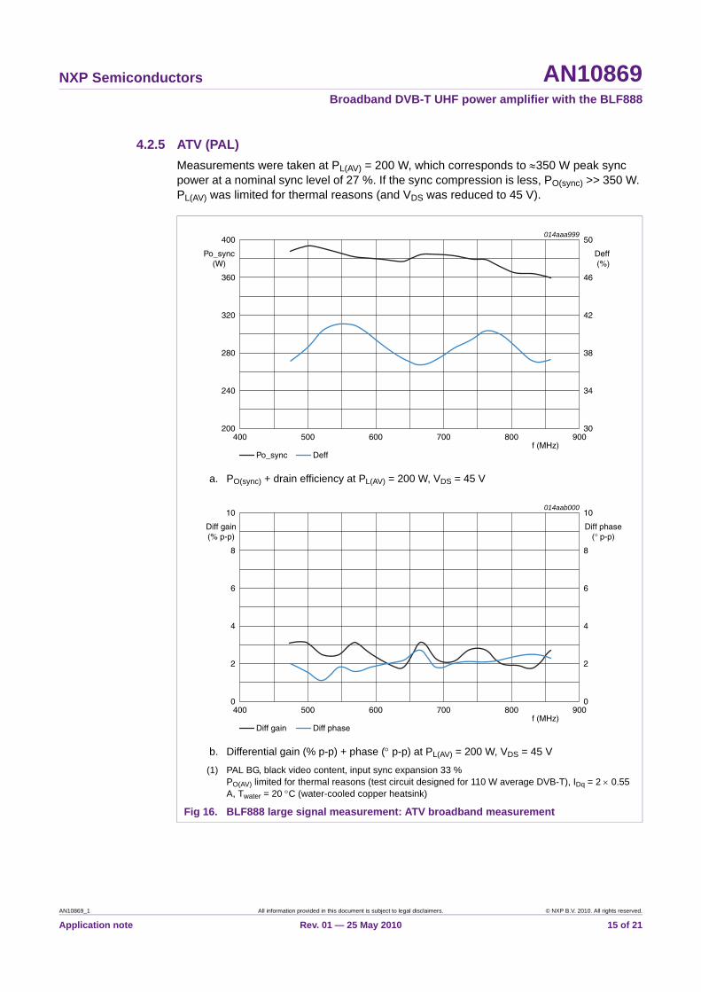
4.2.5 ATV (PAL)Measurements were taken at PL(AV) = 200 W, which corresponds to ≈350 W peak sync power at a nominal sync level of 27 %. If the sync compression is less, PO(sync) >> 350 W. PL(AV) was limited for thermal reasons (and VDS was reduced to 45 V).
a. PO(sync) + drain efficiency at PL(AV) = 200 W, VDS = 45 V
b. Differential gain (% p-p) + phase (° p-p) at PL(AV) = 200 W, VDS = 45 V
(1) PAL BG, black video content, input sync expansion 33 %PO(AV) limited for thermal reasons (test circuit designed for 110 W average DVB-T), IDq = 2 × 0.55 A, Twater = 20 °C (water-cooled copper heatsink)
Fig 16. BLF888 large signal measurement: ATV broadband measurement
014aaa999
f (MHz)400 900800600 700500
280
320
240
360
Po_sync(W)
200
38
42
34
46
50
Deff (%)
30
Po_sync Deff
400
014aab000
f (MHz)400 900800600 700500
4
6
2
8
10
Diff gain(% p-p)
0
4
6
2
8
10
Diff phase(° p-p)
0
Diff gain Diff phase
AN10869_1 All information provided in this document is subject to legal disclaimers. © NXP B.V. 2010. All rights reserved.
Application note Rev. 01 — 25 May 2010 15 of 21
NXP Semiconductors AN10869Broadband DVB-T UHF power amplifier with the BLF888
5. Conclusion
The BLF888 broadband application circuit presented in this report fulfils the following requirements:
• PL(AV) DVB-T > 110 W• Efficiency > 27 % (typ. 29 %)• Shoulder distance < −30 dBc (typ. −35 dBc)• Gain > 18 dB (typ. 20 dB)
The circuit was designed for 110 W average DVB-T. The BLF888 is capable of delivering higher average power levels (e.g. in an ATV application). In such applications, special care must be taken to ensure adequate cooling is provided for the transistor and the circuit will need some redesign to handle the higher average power levels (e.g. the size of balun).
Critical aspects of this broadband design include the harmonic loading (especially the 2nd harmonic of frequencies below 500 MHz), lead contact (an 'air gap' will shift the impedance level significantly) and low frequency stability (several damping resistors were added).
AN10869_1 All information provided in this document is subject to legal disclaimers. © NXP B.V. 2010. All rights reserved.
Application note Rev. 01 — 25 May 2010 16 of 21

NXP Semiconductors AN10869Broadband DVB-T UHF power amplifier with the BLF888
6. Appendix A: PCB layout and Bill of Materials
All dimensions in mm; PCB input = 35 mm × 50 mm, PCB output = 60 mm × 50 mm, M2 holes
Fig 17. Dimensions of BLF888 broadband application circuit
BLF
888
NX
P S
emic
ondu
ctor
s
3 mm
3 mm
14 mm
14 mm
22 mm
16 mm
3 mm
105 mm
23 mm 31 mm3 mm7 mm 3 mm
3 mm
3 mm
3 mm
10 mm
10 mm
24 mm 50 mm
L32
014aab001
Fig 18. Component layout of BLF888 broadband application circuit
001aak652
R3
R5
+VG1(test) +VD1(test)
+VD2(test)+VG2(test)
R7R1
C19
C17
C18
6.5mm
C20
R2
C34
C36
C37
C32C31
C2 C419.5 mm
2 mm
C5 C6
C11
C21
C22
C21
C12
C13
C8
C14
C15
C16
C9
C10
C7C1 C3
R8
C30C3350 Ω 50
Ω
9 mm
31.5 mm
C35
R4
−
−
+
+
R6
AN10869_1 All information provided in this document is subject to legal disclaimers. © NXP B.V. 2010. All rights reserved.
Application note Rev. 01 — 25 May 2010 17 of 21
NXP Semiconductors AN10869Broadband DVB-T UHF power amplifier with the BLF888
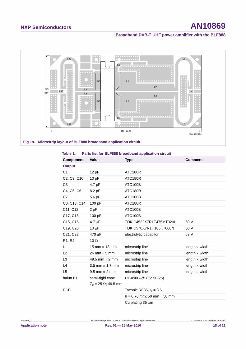
Fig 19. Microstrip layout of BLF888 broadband application circuit
001aak651
L33
L32
L32
105 mm
50mm
L31
L30
L30
L1
L5
L5
L1
L2
L2
L3
L3
L4L31
Table 1. Parts list for BLF888 broadband application circuitComponent Value Type CommentOutputC1 12 pF ATC180R
C2, C9, C10 10 pF ATC180R
C3 4.7 pF ATC100B
C4, C5, C6 8.2 pF ATC180R
C7 5.6 pF ATC100B
C8, C13, C14 100 pF ATC180R
C11, C12 2 pF ATC100B
C17, C18 100 pF ATC100B
C15, C16 4.7 μF TDK C4532X7R1E475MT020U 50 V
C19, C20 10 μF TDK C570X7R1H106KT000N 50 V
C21, C22 470 μF electrolytic capacitor 63 V
R1, R2 10 Ω
L1 15 mm × 13 mm microstrip line length × width
L2 26 mm × 5 mm microstrip line length × width
L3 49.5 mm × 2 mm microstrip line length × width
L4 3.5 mm × 1.7 mm microstrip line length × width
L5 9.5 mm × 2 mm microstrip line length × width
balun B1 semi-rigid coaxZo = 25 Ω; 49.5 mm
UT-090C-25 (EZ 90-25)
PCB Taconic RF35, εr = 3.5
h = 0.76 mm; 50 mm × 50 mm
Cu plating 35 μm
AN10869_1 All information provided in this document is subject to legal disclaimers. © NXP B.V. 2010. All rights reserved.
Application note Rev. 01 — 25 May 2010 18 of 21
NXP Semiconductors AN10869Broadband DVB-T UHF power amplifier with the BLF888
7. Abbreviations
8. References
[1] BLF888 data sheet
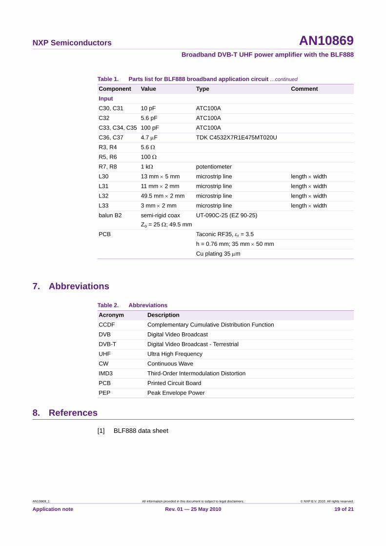
InputC30, C31 10 pF ATC100A
C32 5.6 pF ATC100A
C33, C34, C35 100 pF ATC100A
C36, C37 4.7 μF TDK C4532X7R1E475MT020U
R3, R4 5.6 Ω
R5, R6 100 Ω
R7, R8 1 kΩ potentiometer
L30 13 mm × 5 mm microstrip line length × width
L31 11 mm × 2 mm microstrip line length × width
L32 49.5 mm × 2 mm microstrip line length × width
L33 3 mm × 2 mm microstrip line length × width
balun B2 semi-rigid coaxZo = 25 Ω; 49.5 mm
UT-090C-25 (EZ 90-25)
PCB Taconic RF35, εr = 3.5
h = 0.76 mm; 35 mm × 50 mm
Cu plating 35 μm
Table 1. Parts list for BLF888 broadband application circuit …continued
Component Value Type Comment
Table 2. AbbreviationsAcronym DescriptionCCDF Complementary Cumulative Distribution Function
DVB Digital Video Broadcast
DVB-T Digital Video Broadcast - Terrestrial
UHF Ultra High Frequency
CW Continuous Wave
IMD3 Third-Order Intermodulation Distortion
PCB Printed Circuit Board
PEP Peak Envelope Power
AN10869_1 All information provided in this document is subject to legal disclaimers. © NXP B.V. 2010. All rights reserved.
Application note Rev. 01 — 25 May 2010 19 of 21

NXP Semiconductors AN10869Broadband DVB-T UHF power amplifier with the BLF888
9. Legal information
9.1 DefinitionsDraft — The document is a draft version only. The content is still under internal review and subject to formal approval, which may result in modifications or additions. NXP Semiconductors does not give any representations or warranties as to the accuracy or completeness of information included herein and shall have no liability for the consequences of use of such information.
9.2 DisclaimersLimited warranty and liability — Information in this document is believed to be accurate and reliable. However, NXP Semiconductors does not give any representations or warranties, expressed or implied, as to the accuracy or completeness of such information and shall have no liability for the consequences of use of such information.
In no event shall NXP Semiconductors be liable for any indirect, incidental, punitive, special or consequential damages (including - without limitation - lost profits, lost savings, business interruption, costs related to the removal or replacement of any products or rework charges) whether or not such damages are based on tort (including negligence), warranty, breach of contract or any other legal theory.
Notwithstanding any damages that customer might incur for any reason whatsoever, NXP Semiconductors’ aggregate and cumulative liability towards customer for the products described herein shall be limited in accordance with the Terms and conditions of commercial sale of NXP Semiconductors.
Right to make changes — NXP Semiconductors reserves the right to make changes to information published in this document, including without limitation specifications and product descriptions, at any time and without notice. This document supersedes and replaces all information supplied prior to the publication hereof.
Suitability for use — NXP Semiconductors products are not designed, authorized or warranted to be suitable for use in life support, life-critical or safety-critical systems or equipment, nor in applications where failure or malfunction of an NXP Semiconductors product can reasonably be expected to result in personal injury, death or severe property or environmental damage. NXP Semiconductors accepts no liability for inclusion and/or use of NXP Semiconductors products in such equipment or applications and therefore such inclusion and/or use is at the customer’s own risk.
Applications — Applications that are described herein for any of these products are for illustrative purposes only. NXP Semiconductors makes no representation or warranty that such applications will be suitable for the specified use without further testing or modification.
Customers are responsible for the design and operation of their applications and products using NXP Semiconductors products, and NXP Semiconductors accepts no liability for any assistance with applications or customer product design. It is customer’s sole responsibility to determine whether the NXP Semiconductors product is suitable and fit for the customer’s applications and products planned, as well as for the planned application and use of customer’s third party customer(s). Customers should provide appropriate design and operating safeguards to minimize the risks associated with their applications and products.
NXP Semiconductors does not accept any liability related to any default, damage, costs or problem which is based on any weakness or default in the customer’s applications or products, or the application or use by customer’s third party customer(s). Customer is responsible for doing all necessary testing for the customer’s applications and products using NXP Semiconductors products in order to avoid a default of the applications and the products or of the application or use by customer’s third party customer(s). NXP does not accept any liability in this respect.
Export control — This document as well as the item(s) described herein may be subject to export control regulations. Export might require a prior authorization from national authorities.
9.3 Licenses
9.4 TrademarksNotice: All referenced brands, product names, service names and trademarks are the property of their respective owners.
ICs with DVB-T or DVB-T2 functionality
Use of this product in any manner that complies with the DVB-T or the DVB-T2 standard may require licenses under applicable patents of the DVB-T respectively the DVB-T2 patent portfolio, which license is available from Sisvel S.p.A., Via Sestriere 100, 10060 None (TO), Italy, and under applicable patents of other parties.
AN10869_1 All information provided in this document is subject to legal disclaimers. © NXP B.V. 2010. All rights reserved.
Application note Rev. 01 — 25 May 2010 20 of 21

NXP Semiconductors AN10869Broadband DVB-T UHF power amplifier with the BLF888
10. Contents
1 Introduction . . . . . . . . . . . . . . . . . . . . . . . . . . . . 32 Circuit description . . . . . . . . . . . . . . . . . . . . . . . 33 Design and Simulation . . . . . . . . . . . . . . . . . . . 63.1 BLF888 impedance and simulation data . . . . . 63.1.1 Impedance data . . . . . . . . . . . . . . . . . . . . . . . . 63.1.2 Simulation data . . . . . . . . . . . . . . . . . . . . . . . . . 73.2 Bias and decoupling circuit . . . . . . . . . . . . . . . . 83.3 Thermal considerations . . . . . . . . . . . . . . . . . . 84 Test results . . . . . . . . . . . . . . . . . . . . . . . . . . . . . 84.1 Small signal measurements . . . . . . . . . . . . . . . 84.2 Large signal measurements . . . . . . . . . . . . . . . 94.2.1 DVB-T. . . . . . . . . . . . . . . . . . . . . . . . . . . . . . . . 94.2.2 2-tone . . . . . . . . . . . . . . . . . . . . . . . . . . . . . . . 124.2.3 Pulsed. . . . . . . . . . . . . . . . . . . . . . . . . . . . . . . 134.2.4 CW . . . . . . . . . . . . . . . . . . . . . . . . . . . . . . . . . 144.2.5 ATV (PAL) . . . . . . . . . . . . . . . . . . . . . . . . . . . . 155 Conclusion . . . . . . . . . . . . . . . . . . . . . . . . . . . . 166 Appendix A: PCB layout and Bill of Materials 177 Abbreviations. . . . . . . . . . . . . . . . . . . . . . . . . . 198 References . . . . . . . . . . . . . . . . . . . . . . . . . . . . 199 Legal information. . . . . . . . . . . . . . . . . . . . . . . 209.1 Definitions. . . . . . . . . . . . . . . . . . . . . . . . . . . . 209.2 Disclaimers . . . . . . . . . . . . . . . . . . . . . . . . . . . 209.3 Licenses . . . . . . . . . . . . . . . . . . . . . . . . . . . . . 209.4 Trademarks. . . . . . . . . . . . . . . . . . . . . . . . . . . 2010 Contents . . . . . . . . . . . . . . . . . . . . . . . . . . . . . . 21
© NXP B.V. 2010. All rights reserved.For more information, please visit: http://www.nxp.comFor sales office addresses, please send an email to: [email protected]
Date of release: 25 May 2010Document identifier: AN10869_1
Please be aware that important notices concerning this document and the product(s)described herein, have been included in section ‘Legal information’.