Embed Size (px)
Citation preview
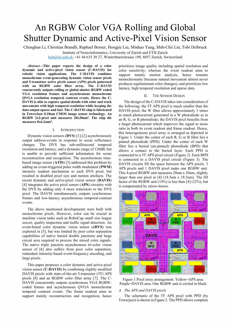
An RGBW Color VGA Rolling and Global
Shutter Dynamic and Active-Pixel Vision Sensor Chenghan Li, Christian Brandli, Raphael Berner, Hongjie Liu, Minhao Yang, Shih-Chii Liu, Tobi Delbruck
Institute of Neuroinformatics, University of Zurich and ETH Zurich
[email protected], +41 44 635 30 27, Winterthurerstrasse 190, 8057 Zurich, Switzerland
Abstract—This paper reports the design of a color
dynamic and active-pixel vision sensor (C-DAVIS) for
robotic vision applications. The C-DAVIS combines
monochrome event-generating dynamic vision sensor pixels
and 5-transistor active pixels sensor (APS) pixels patterned
with an RGBW color filter array. The C-DAVIS
concurrently outputs rolling or global shutter RGBW coded
VGA resolution frames and asynchronous monochrome
QVGA resolution temporal contrast events. Hence the C-
DAVIS is able to capture spatial details with color and track
movements with high temporal resolution while keeping the
data output sparse and fast. The C-DAVIS chip is fabricated
in TowerJazz 0.18um CMOS image sensor technology. An
RGBW 2x2-pixel unit measures 20x20um2. The chip die
measures 8x6.2mm2.
I. INTRODUCTION
Dynamic vision sensors (DVS) [1]-[2] asynchronously
output address-events in response to scene reflectance
changes. The DVS has sub-millisecond temporal
resolution and latency, and a dynamic range of 120dB, but
is unable to provide sufficient information for scene
reconstruction and recognition. The asynchronous time-
based image sensor (ATIS) [3] addressed this problem by
adding an event-triggered pulse width modulated (PWM)
intensity readout mechanism to each DVS pixel, but
resulted in doubled pixel size and motion artefacts. The
recent dynamic and active-pixel vision sensor (DAVIS)
[4] integrates the active pixel sensor (APS) circuitry with
the DVS by adding only 4 more transistors to the DVS
pixel. The DAVIS simultaneously outputs synchronous
frames and low-latency asynchronous temporal-contrast
events.
The above mentioned developments were built with
monochrome pixels. However, color can be crucial in
machine vision tasks such as RoboCup small size league
soccer, quality inspection and traffic signal detection. An
event-based color dynamic vision sensor (cDVS) was
explored in [5], but was limited by poor color separation
capabilities of native buried double junctions and large
circuit area required to process the mixed color signals.
The native triple junction asynchronous tri-color vision
sensor of [6] also suffers from poor color separation,
redundant intensity-based event-frequency encoding, and
large pixels.
This paper proposes a color dynamic and active-pixel
vision sensor (C-DAVIS) by combining slightly modified
DAVIS pixels with state-of-the-art 5-transistor (5T) APS
pixels [8] and an RGBW color filter array [7]. The C-
DAVIS concurrently outputs synchronous VGA RGBW-
coded frames and asynchronous QVGA monochrome
temporal contrast events. The frame readout aims to
support mainly reconstruction and recognition, hence
prioritizes image quality including spatial resolution and
color sensitivity; whereas the event readout aims to
support mainly motion analysis, hence remains
monochromatic (because natural movement almost never
produces equiluminant color changes), and prioritizes low
latency, high temporal resolution and sparse data.
II. THE SENSOR DESIGN
The design of the C-DAVIS takes into consideration of
the following: the 5T APS pixel is much smaller than the
DAVIS pixel; the W filter allows approximately 3 times
as much photocurrent generated in a W photodiode as in
an R, G, or B photodiode; the DAVIS pixel benefits from
a larger photocurrent which improves the signal to noise
ratio in both its event readout and frame readout. Hence,
this heterogeneous pixel array is arranged as depicted in
Figure 1. Under the center of each R, G or B filter lies a
pinned photodiode (PPD). Under the center of each W
filter lies a buried (un-pinned) photodiode (BPD) that
allows a contact to the buried layer. Each PPD is
connected to a 5T APS pixel circuit (Figure 2). Each BPD
is connected to a DAVIS pixel circuit (Figure 3). The
DAVIS circuits fill the space between the APS pixels. 3
APS pixels and 1 DAVIS pixel make one RGBW unit.
This 4-pixel RGBW unit measures 20um x 20um, slightly
larger than one pixel in [4] (18.5um x 18.5um). The fill
factor of the RGBW unit (14%) is less than [4] (22%), but
is compensated by micro-lenses.
Figure 1 Pixel array arrangement. Yellow=APS area. Purple=DAVIS area. One RGBW unit is circled in black.
A. The APS and DAVIS pixels
The schematic of the 5T APS pixel with PPD (by Towerjazz) is shown in Figure 2. The PPD allows complete
charge transfer from the PPD to the floating diffusion FD. MN1 is the overflow gate (OVG2) which sets the overflow level of the PPD and resets the PPD. MN2 is the transfer gate (TX2). MN3 is the reset switch (RST) that resets FD. MN4 is the source follower readout input transistor. MN5 is the row select switch (SEL) for the analog output (AO) readout. The pixel function is explained in [8].
MN1
MN2 MN4
MN5
OVG2TX2
SEL
AO
3.3V 3.3 V
PPD
RST
3.3 V
MN3
FDVPD
Figure 2 The 5T APS circuit.
A simplified diagram of a DAVIS pixel circuit is shown in Figure 3. Similar to [4], the DAVIS circuit consists of two parts, the “APS part” and the “DVS part”. The “APS part” is modified from [4] by adding the reset switch MN3 and the integration capacitor CP. The reason for this change is to make the DAVIS pixel controllable in the same way as the 5T APS pixel for the frame readout (see section III). The “DVS part” is borrowed from [4] but with a revamped layout to fit the space between the APS pixels. The “DVS part” communicates an ON event through the address event representation (AER) logic block when there is an increase in brightness (log intensity) and an OFF event when there is a decrease in brightness.
MP1
MN8
MN6
MN7
MN1
MN2 MN4
MN5
-AAER
Logic
C2
C1
CR
ON
CA
CR
OF
F
Bias1
Bias2
OVG1TX1
SEL
1
AO
3.3V 3.3 V
1.8 V
Vdiff
S1
APS
Part
DVS
Part
Switched cap
Differential amplifier
BPD
Com
pa
rato
rs
Vpr
RST
3.3 V
MN3
FD
VCP CP
3.3V
Figure 3 The DAVIS pixel circuit.
The frame readout comes from the APS pixels and the
“APS part” of the DAVIS pixels, and employs a unified
timing control for both the APS and the DAVIS pixels to
reduce complexity. The frame readout can switch between
rolling and global shutter modes. The event readout is the
same as [4], communicating ON/OFF events through the
address event representation (AER) logic when there is an
increase/decrease in log intensity.
B. The frame readout logic
The frame readout logic employs unified timing control for both the APS and the DAVIS pixels to reduce logic and wiring complexity. RST and SEL signals are shared among the APS and the DAVIS. OVG1 and OVG2 share the same timing but have separate programmable logic high and low levels. The same goes for TX1 and TX2. The readout has both rolling and global shutter modes.
The rolling shutter control scheme is explained with the timing diagram in Figure 4.
Row n
Row n+1
TX1
TX2
RST
SEL
TX1
TX2
RST
SEL
VCP
VFD
V2V1
VPD
VFD
OVG2
DAVIS
APS
Row n+1
OVG1
OVG2
OVG1
V3 Figure 4 Rolling shutter timing diagram.
In a DAVIS pixel, the photocurrent integrates on CP. VCP saturates when it reaches one threshold below OVG1. In an APS pixel, the photocurrent integrates on the PPD. The PPD’s saturation level is determined by OVG2. When a row is selected, RST is turned off and the reset level V1 is sampled via AO. Then TX1 and TX2 are turned on to perform charge sharing between CP and FD in the DAVIS and charge transfer from PPD to FD in the APS. When TX1 and TX2 are turned off, the exposure of this row ends. The signal level V2 is then sampled via AO. In the APS, charge accumulated on PPD is completely transferred to FD, so the accumulated charge QAPS can be computed via correlated double sampling (CDS) off-chip as:
𝑄𝐴𝑃𝑆 = 𝐶𝐹𝐷 ∙ (𝑉1 − 𝑉2)
In the DAVIS, charge accumulated on CP is not completely transferred to FD. To compute the amount of accumulated charge QDAVIS, a third sample is needed. OVG1 and OVG2 are turned on to reset CP and PPD. Meanwhile TX1 and TX2 are turned on. Immediately after OVG1 and OVG2 are turned off, TX1 and TX2 are also switched off. A third sample V3 is obtained though AO. V3 is irrelevant to the APS. But in the DAVIS, V3 is the reset level of CP. And QDAVIS can be computed off-chip as:
𝑄𝐷𝐴𝑉𝐼𝑆 = 𝐶𝐹𝐷 ∙ (𝑉1 − 𝑉2) + 𝐶𝑃 ∙ (𝑉3 − 𝑉2)
Triple sampling is performed in the DAVIS to remove the
fixed pattern noise (FPN) caused by offsets in the reset
levels of both CP and FD. However, the three samples are
uncorrelated and the kTC noise introduced by TX1 and
OVG1 cannot be removed. The three samples are acquired
with minimum temporal separation in order to minimize
1/f noise introduced by MN4 [9]. 3 samples per row-select
may increase the individual row time and thus motion
distortions. However, for the C-DAVIS, rolling shutter
readout is meant for capturing static scenes. When the
frame readout is distorted due to motion, the asynchronous
event readout could allow off chip corrections.
The global shutter control scheme minimizes motion artefacts, but with the tradeoff of higher noise. The timing diagram is illustrated in Figure 5.
SEL
RST
TX1
OVG1
VCP
VFD
FOT ROT
VPD
VFD
TX2
DAVIS
APS
V1 V2
OVG2
V3
Figure 5 Global shutter timing diagram.
During the global frame overhead time (FOT), OVG1 and OVG2 are lowered to initiate the exposure. Exposure is ended by simultaneously turning TX1 and TX2 off. At the end of the exposure, each pixel has stored a signal level in its FD for the row by row readout.
During a row overhead time (ROT), one row is selected by turning SEL on. The signal level V1 is sampled via AO, followed by a RST pulse, then a sample of the reset level V2 via AO. In the APS, the accumulated charge QAPS can be computed off-chip as below:
𝑄𝐴𝑃𝑆 = 𝐶𝐹𝐷 ∙ (𝑉2 − 𝑉1)
In the DAVIS, a third sample is needed to compute QDAVIS. TX1 and TX2 are turned on and OVG1 and OVG2 are turned off to allow FD to sample the reset level of CP. After TX1 and TX2 are turned off, the third sample V3 is obtained. And QDAVIS can be computed off-chip as:
𝑄𝐷𝐴𝑉𝐼𝑆 = 𝐶𝐹𝐷 ∙ (𝑉2 − 𝑉1) + 𝐶𝑃 ∙ (𝑉3 − 𝑉1)
The global shutter control scheme performs differential double sampling in the APS and triple sampling in the DAVIS which removes FPN caused by offsets in the reset levels of FD and CP. But kTC noise introduced by RST and TX1 will remain. Because global shutter requires high shutter efficiency, both the APS and the DAVIS pixel have metal shielding and dedicated implants to reduce FD leakage. Moreover, the control logic is designed to have the flexibility to implement a different double sampling global shutter control scheme as seen in [4] to cancel out the effect of FD leakage in reset and signal samples, at the cost of increased 1/f noise.
C. The integration
To output uniform frames from this heterogeneous
pixel array, the frame readout of the APS and the DAVIS
pixels should have matching parameters. The APS pixel’s
conversion gain is determined solely by the capacitance of
FD, while the DAVIS pixel’s conversion gain is
determined by both the capacitance of FD and CP.
Considering that the BPD receives approximately 3 times
as many photons as the PPD receives under natural
illumination, due to the optical efficiency difference
between R, G, B and W filters, the combined capacitance
of FD and CP is designed to be 3 times of the capacitance
of FD. Also, the integration capacity of the DAVIS is
designed to be 3 times of the APS. This way, although a
DAVIS BPD receives approximately 3 times as many
photons as an APS PPD, two types of pixels saturate at
about the same time during exposure and have similar
range of output swing.
Because the heterogeneous pixel array concurrently
produces both frame and event outputs, significant design
efforts were spent on minimizing crosstalk between the
frame readout and the event readout. As a lesson learned
from [4], the largest disturbance comes from the frame
readout control signals, especially in global shutter mode.
To reduce their impact on the event readout, careful signal
separation and shielding were done in pixel layout. All
frame readout control signals are driven by buffers with
programmable slew rate. All event readout biases are
driven by programmable analog buffers distributed in
every column.
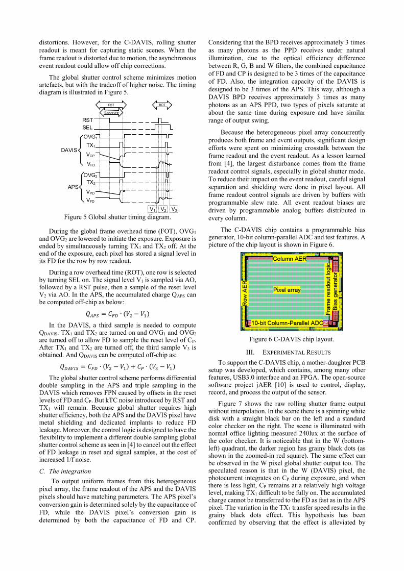
The C-DAVIS chip contains a programmable bias generator, 10-bit column-parallel ADC and test features. A picture of the chip layout is shown in Figure 6.
Figure 6 C-DAVIS chip layout.
III. EXPERIMENTAL RESULTS
To support the C-DAVIS chip, a mother-daughter PCB setup was developed, which contains, among many other features, USB3.0 interface and an FPGA. The open-source software project jAER [10] is used to control, display, record, and process the output of the sensor.
Figure 7 shows the raw rolling shutter frame output without interpolation. In the scene there is a spinning white disk with a straight black bar on the left and a standard color checker on the right. The scene is illuminated with normal office lighting measured 240lux at the surface of the color checker. It is noticeable that in the W (bottom-left) quadrant, the darker region has grainy black dots (as shown in the zoomed-in red square). The same effect can be observed in the W pixel global shutter output too. The speculated reason is that in the W (DAVIS) pixel, the photocurrent integrates on CP during exposure, and when there is less light, CP remains at a relatively high voltage level, making TX1 difficult to be fully on. The accumulated charge cannot be transferred to the FD as fast as in the APS pixel. The variation in the TX1 transfer speed results in the grainy black dots effect. This hypothesis has been confirmed by observing that the effect is alleviated by

increasing the charge transfer time. However, increasing charge transfer time is not able to eliminate this effect. In the follow-up experiments, a different global shutter readout logic [4] will be tested, which is a possible solution to achieve good performance in both the DAVIS and the APS frame output.
Figure 7 Rolling shutter frame output without interpolation. The four quadrants corresponds to
(clockwise from top-left): the R (APS) pixels, G (APS) pixels, B (APS) pixels and W (DAVIS) pixels.
Figure 8 shows the space-time view of the dual-output data of the same scene with the same illumination (240lux). The full color VGA frame is achieved by simple linear interpolation only (excluding W pixels). The 306ms time slice contains 1 million events, which clearly trace the rotation of the black bar with high temporal resolution.
Figure 8 Space-time view of the dual-output, the interpolated full color frame and the events from the rotating black bar on the white disk. Green events are
older, red events are newer.
Table 1 summarizes the specifications of the chip in comparison to [4]. The significant increase in power consumption compared to [4] is due to the increase in pixel numbers, more complex APS control logic circuitry and the on-chip column parallel ADC. The event readout alone only consumes about 15-32mW depending on the amount of movement in the scene. Other key characteristics such as the dynamic range, FPN, dark signal of the frame output
and the latency, bandwidth, sensitivity of the event output will be measured in the follow-up experiments.
Table 1 C-DAVIS vs. DAVIS Design Specifications This work DAVIS [4]
Fabrication process
6M1P 0.18um CIS process with MIM
6M1P 0.18um CIS process with MIM
Supply voltage 3.3V analog
1.8V/4V digital 3.3V analog 1.8V digital
Resolution 640 x 480 Frame 320 x 240 Event
240 x 180 frame and event
Pixel size 2x2 pixels: 20x20um2 1 pixel: 18.5x18.5um2
Pixel complexity
2x2 pixels: 56 fets 3 MIMcaps
4 photodiodes
1 pixel: 44 fets 2 MIMcaps
1 photodiodes
Fill factor 14% (not considering
micro-lenses) 22%
Die size 8x6.2mm2 5x5mm2
Power consumption
106-120mW 5-14mW
IV. DISCUSSION
By combining the DAVIS and the APS, the C-DAVIS is able to utilize the focal plane area and fit under a standard RGBW color filter array. Although the proposed triple sampling frame readout increases the amount of data per frame, for robotic vision applications the frame rate is designed to be data-driven with the help of the event readout. The frame readout logic is also flexible and allows double sampling as [4]. The initial testing has found the chip functional as designed. Further experiment results will be reported later.
ACKNOWLEDGMENT
The authors thank Towerjazz for technical support, Vicente Villanueva for building the PCBs, Luca Longinotti for building the firmware, logic and user interface.
REFERENCES
[1] P. Lichtsteiner, C. Posch, and T. Delbruck, “A 128 x 128 120 dB 15µs Latency Asynchronous Temporal Contrast Vision Sensor,” IEEE J. Solid-State Circuits, vol. 43, no. 2, pp. 566–576, 2008.
[2] T. Delbruck, B. Linares-Barranco, E. Culurciello, and C. Posch, “Activity-Driven, Event-Based Vision Sensors,” in Proceedings of 2010 IEEE International Symposium on Circuits and Systems (ISCAS), 2010, pp. 2426-2429.
[3] C. Posch, D. Matolin, and R. Wohlgenannt, “A QVGA 143 dB Dynamic Range Frame-Free PWM Image Sensor with Lossless Pixel-Level Video Compression and Time-Domain CDS,” IEEE J. Solid-State Circuits, vol. 46, no. 1, pp. 259–275, Jan. 2011.
[4] C. Brandli, R. Berner, M. Yang, S.-C. Liu, T. Delbruck, "A 240 × 180 130 dB 3 µs Latency Global Shutter Spatiotemporal Vision Sensor," IEEE J. Solid-State Circuits, vol.49, no.10, pp.2333-2341, Oct 2014.
[5] R. Berner, and T. Delbruck, “Event-Based Pixel Sensitive to Changes of Color and Brightness,” IEEE Transactions on Circuits and Systems I: Regular Papers, 58:(7) 1581-1590, 2011
[6] J. A. Lenero-Bardallo, D. H. Bryn, and P. Hafliger, "Bio-inspired Asynchronous Pixel Event Tri-color Vision Sensor", IEEE Transactions on Biomedical Circuit and Systems, vol. 8, No. 3, pp. 345-357, ISSN: 1932-4545, June 2014.
[7] T. Sugiyama, “Image-Capturing Apparatus” U.S. Patent 20050231618 A1. Oct, 20, 2005.
[8] E. C. Fox, and N. O, “Pinned Photodiode Five Transistor Pixel” U.S. Patent 6 566 697 B1. May, 20, 2003.
[9] H. Tian, B. Fowler, and A.E. Gamal, "Analysis of temporal noise in CMOS photodiode active pixel sensor," IEEE J. Solid-State Circuits, , vol.36, no.1, pp.92,101, Jan 2001
[10] jAER Open Source Project: http://sourceforge.net/projects/jaer/


![Flexstrip 115 RGBW Rot Spectrum - AUTLED · Flexstrip 115 RGBW Rot . Spectrum . Measurement name: FS-115-RGBW Rot. Measurement time: 2016-04-19 14:14:05 ... 49.7798 Power [W] 26,04](https://img.pdfslide.us/doc/110x75/5b9303f209d3f280378c6cc4/flexstrip-115-rgbw-rot-spectrum-flexstrip-115-rgbw-rot-spectrum-measurement.jpg)