Embed Size (px)
Citation preview

AN OVERVIEW OF EMBEDDED SELF-TEST DESIGN
A report by
Gaurav Gulati Ryan Fonnesbeck
Sathya Vijayakumar Sudheesh Madayi

Acknowledgements Our sincere thanks to Dr. Kalla for giving us this opportunity to work on this topic and guiding us throughout. Many thanks to our friends and family who have been supportive throughout the course of this project. Lastly, we do need to acknowledge each other for the cooperation and efforts put in by each of us to successfully complete this project.
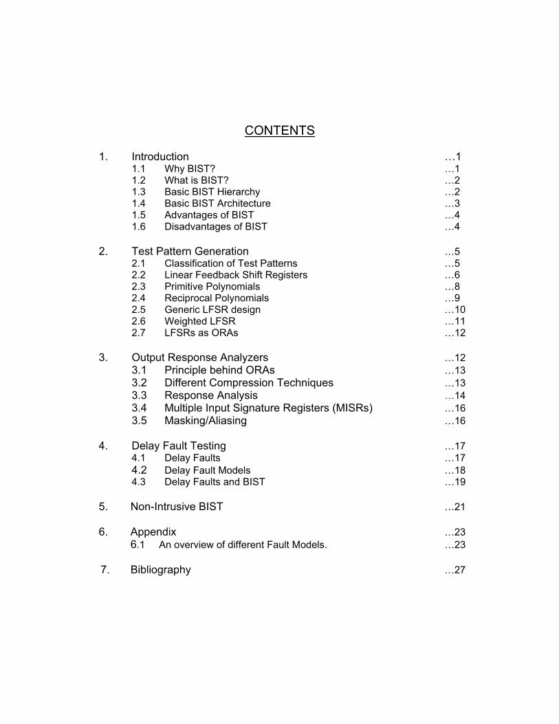
CONTENTS
1. Introduction …1 1.1 Why BIST? …1 1.2 What is BIST? …2 1.3 Basic BIST Hierarchy …2 1.4 Basic BIST Architecture …3 1.5 Advantages of BIST …4 1.6 Disadvantages of BIST …4
2. Test Pattern Generation …5
2.1 Classification of Test Patterns …5 2.2 Linear Feedback Shift Registers …6 2.3 Primitive Polynomials …8 2.4 Reciprocal Polynomials …9 2.5 Generic LFSR design …10 2.6 Weighted LFSR …11 2.7 LFSRs as ORAs …12
3. Output Response Analyzers …12
3.1 Principle behind ORAs …13 3.2 Different Compression Techniques …13 3.3 Response Analysis …14 3.4 Multiple Input Signature Registers (MISRs) …16 3.5 Masking/Aliasing …16
4. Delay Fault Testing …17
4.1 Delay Faults …17 4.2 Delay Fault Models …18 4.3 Delay Faults and BIST …19
5. Non-Intrusive BIST …21
6. Appendix …23
6.1 An overview of different Fault Models. …23
7. Bibliography …27

1 1. INTRODUCTION
This report contains an overview of Built In Self-Test (BIST), its significance, its generic architecture (with detailed coverage of all the components), and its advantages and disadvantages. 1.1 Why BIST?
Have you ever wondered about the reliability of electronic circuits aboard satellites and space shuttles? Once launched in space how do these systems maintain their functional integrity? How does one detect and diagnose any malfunctions from the earth stations? BIST is a testing paradigm that offers a solution to these questions.
To understand the need for BIST one needs to be aware of the various testing procedures involved during the design and manufacture of any system. There are three main phases in the design cycle of a product where testing plays a crucial role:
Design Verification: where the design is tested to check if it satisfies the
system specification. Simulating the design under test with respect to logic, switching levels and timing performs this.
Testing for Manufacturing Defects: consists again of wafer level testing and device level testing. In the former, a chip on a wafer is tested and if passed, is packaged to form a device and hence thereby giving rise to the latter. “Burn-in testing” – an important part in this category, tests the circuit under test (CUT) under extreme ratings (high end values) of temperature, voltage and other operational parameters such as speed. “Burn-in testing” proves to be very expensive when testers are used externally to generate test vectors and observe the output response for failures.
System Operation: A system may be implemented using a chip-set where each chip takes on a specific system function. Once a system has been completely fabricated at the board level, it still needs to be tested for any printed circuit board (PCB) faults that might affect operation. For this purpose concurrent fault detection circuits (CFDCs), that make use of error correction codes such as parity or cyclic redundancy check (CRC), are used to determine if and when a fault occurs during system operation.
With the above outline of the different kinds of testing involved at various
stages of a product design cycle, we now move on to the problems associated with these testing procedures. The number of transistors contained in most VLSI devices today have increased four orders of magnitude for every order increase in the number of I/O (input-output) pins [3]. Add to it the surface mounting of components and the implementation of embedded core functions – all these make the device less accessible from the point of view of testing, making testing a big challenge. With increasing device sizes and decreasing component sizes, the number and types of defects that can occur during manufacturing increase drastically, thereby increasing the cost of testing. Due to the growing complexity
2of VLSI devices and system PCBs, the ability to provide some level of fault diagnosis (information regarding the location and possibly the type of the fault or defect) during manufacturing testing is needed to assist failure mode analysis (FMA) for yield enhancement and repair procedures. This is why BIST is needed! BIST can partition the device into levels and then perform testing.
BIST offers a hierarchical solution to the testing problem such that the
burden on the system level test is reduced. The same testing approach could be used to cover wafer and device level testing, manufacturing testing as well as system level testing in the field where the system operates. Hence, BIST provides for Vertical Testability. 1.2 What is BIST?
The basic concept of BIST involves the design of test circuitry around a system that automatically tests the system by applying certain test stimulus and observing the corresponding system response. Because the test framework is embedded directly into the system hardware, the testing process has the potential of being faster and more economical than using an external test setup. One of the first definitions of BIST was given as:
“…the ability of logic to verify a failure-free status automatically, without
the need for externally applied test stimuli (other than power and clock), and without the need for the logic to be part of a running system.” –Richard M. Sedmak [3]. 1.3 Basic BIST Hierarchy
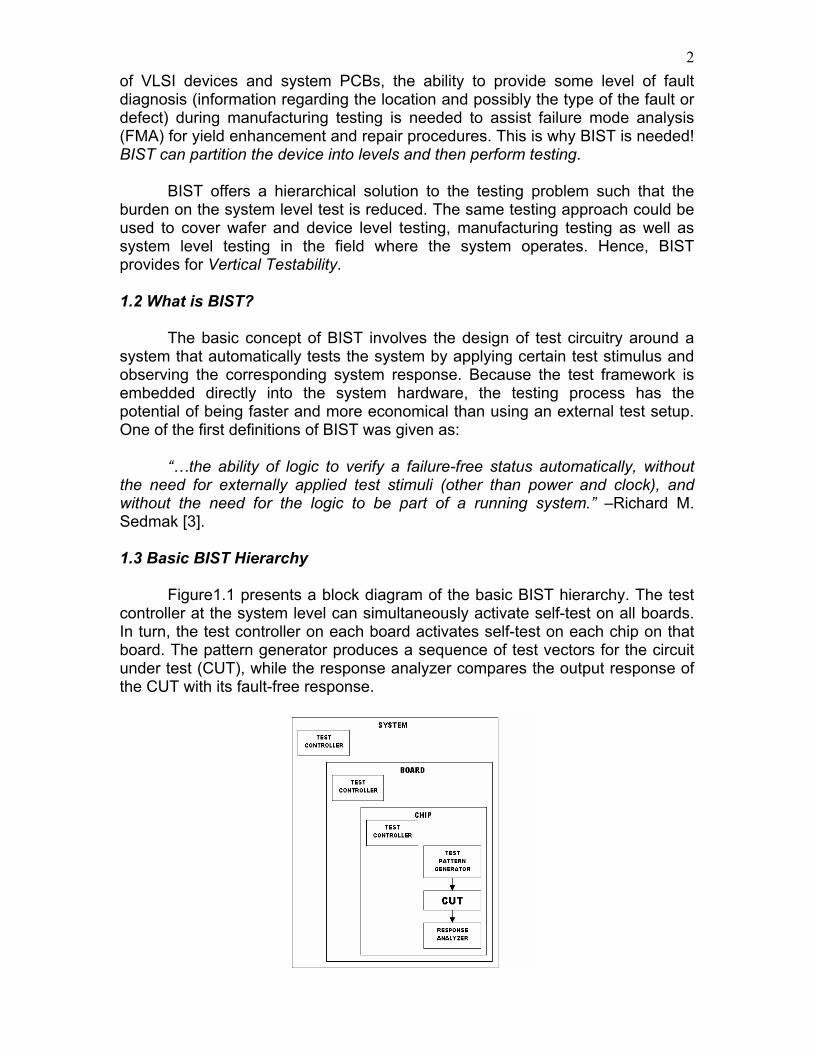
Figure1.1 presents a block diagram of the basic BIST hierarchy. The test controller at the system level can simultaneously activate self-test on all boards. In turn, the test controller on each board activates self-test on each chip on that board. The pattern generator produces a sequence of test vectors for the circuit under test (CUT), while the response analyzer compares the output response of the CUT with its fault-free response.
3 Figure 1.1: Basic BIST Hierarchy.
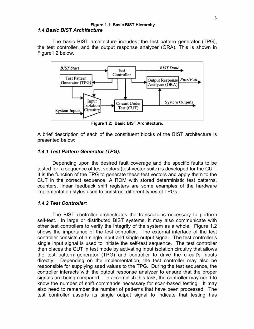
1.4 Basic BIST Architecture The basic BIST architecture includes: the test pattern generator (TPG), the test controller, and the output response analyzer (ORA). This is shown in Figure1.2 below.
Figure 1.2: Basic BIST Architecture.
A brief description of each of the constituent blocks of the BIST architecture is presented below:
1.4.1 Test Pattern Generator (TPG):
Depending upon the desired fault coverage and the specific faults to be
tested for, a sequence of test vectors (test vector suite) is developed for the CUT. It is the function of the TPG to generate these test vectors and apply them to the CUT in the correct sequence. A ROM with stored deterministic test patterns, counters, linear feedback shift registers are some examples of the hardware implementation styles used to construct different types of TPGs. 1.4.2 Test Controller:
The BIST controller orchestrates the transactions necessary to perform self-test. In large or distributed BIST systems, it may also communicate with other test controllers to verify the integrity of the system as a whole. Figure 1.2 shows the importance of the test controller. The external interface of the test controller consists of a single input and single output signal. The test controller’s single input signal is used to initiate the self-test sequence. The test controller then places the CUT in test mode by activating input isolation circuitry that allows the test pattern generator (TPG) and controller to drive the circuit’s inputs directly. Depending on the implementation, the test controller may also be responsible for supplying seed values to the TPG. During the test sequence, the controller interacts with the output response analyzer to ensure that the proper signals are being compared. To accomplish this task, the controller may need to know the number of shift commands necessary for scan-based testing. It may also need to remember the number of patterns that have been processed. The test controller asserts its single output signal to indicate that testing has

4completed, and that the output response analyzer has determined whether the circuit is faulty or fault-free. 1.4.3 Output Response Analyzer (ORA): The response of the system to the applied test vectors needs to be analyzed and a decision made about the system being faulty or fault-free. This function of comparing the output response of the CUT with its fault-free response is performed by the ORA. The ORA compacts the output response patterns from the CUT into a single pass/fail indication. Response analyzers may be implemented in hardware by making used of a comparator along with a ROM based lookup table that stores the fault-free response of the CUT. The use of multiple input signature registers (MISRs) is one of the most commonly used techniques for ORA implementations.
Let us take a look at a few of the advantages and disadvantages – now that we have a basic idea of the concept of BIST. 1.5 Advantages of BIST
Vertical Testability: The same testing approach could be used to cover wafer and device level testing, manufacturing testing as well as system level testing in the field where the system operates.
Reduction in Testing Costs: The inclusion of BIST in a system design minimizes the amount of external hardware required for carrying out testing significantly. A 400 pin system on chip design not implementing BIST would require a huge (and costly) 400 pin tester, when compared with a 4 pin (vdd, gnd.,clock and reset) tester required for its counter part having BIST implemented.
In-Field Testing capability: Once the design is functional and operating in the field, it is possible to remotely test the design for functional integrity using BIST, without requiring direct test access.
Robust/Repeatable Test Procedures: The use of automatic test equipment (ATE) generally involves the use of very expensive handlers, which move the CUTs onto a testing framework. Due to its mechanical nature, this process is prone to failure and cannot guarantee consistent contact between the CUT and the test probes from one loading to the next. In BIST, this problem is minimized due to the significantly reduced number of contacts necessary.
1.6 Disadvantages of BIST
Area Overhead: The inclusion of BIST in a particular system design results in greater consumption of die area when compared to the original system design. This may seriously impact the cost of the chip as the yield per wafer reduces with the inclusion of BIST.
Performance penalties: The inclusion of BIST circuitry adds to the combinational delay between registers in the design. Hence, with the inclusion of BIST the maximum clock frequency at which the original design could operate will reduce, resulting in reduced performance.

5 Additional Design time and Effort: During the design cycle of the
product, resources in the form of additional time and man power will be devoted for the implementation of BIST in the designed system.
Added Risk: What if the fault existed in the BIST circuitry while the CUT operated correctly. Under this scenario, the whole chip would be regarded as faulty, even though it could perform its function correctly.
The advantages of BIST outweigh its disadvantages. As a result, BIST is
implemented in a majority of the electronic systems today, all the way from the chip level to the integrated system level.
2. TEST PATTERN GENERATION The fault coverage that we obtain for various fault models is a direct function of the test patterns produced by the Test Pattern Generator (TPG) and applied to the CUT. This section presents an overview of some basic TPG implementation techniques used in BIST approaches. 2.1 Classification of Test Patterns
There are several classes of test patterns. TPGs are sometimes classified according to the class of test patterns that they produce. The different classes of test patterns are briefly described below:
Deterministic Test Patterns: These test patterns are developed to detect specific faults and/or structural defects for a given CUT. The deterministic test vectors are stored in a ROM and the test vector sequence applied to the CUT is controlled by memory access control circuitry. This approach is often referred to as the “ stored test patterns “ approach.
Algorithmic Test Patterns: Like deterministic test patterns, algorithmic test patterns are specific to a given CUT and are developed to test for specific fault models. Because of the repetition and/or sequence associated with algorithmic test patterns, they are implemented in hardware using finite state machines (FSMs) rather than being stored in a ROM like deterministic test patterns.
Exhaustive Test Patterns: In this approach, every possible input combination for an N-input combinational logic is generated. In all, the exhaustive test pattern set will consist of 2N test vectors. This number could be really huge for large designs, causing the testing time to become significant. An exhaustive test pattern generator could be implemented using an N-bit counter.
Pseudo-Exhaustive Test Patterns: In this approach the large N-input combinational logic block is partitioned into smaller combinational logic sub-circuits. Each of the M-input sub-circuits (M<N) is then exhaustively tested by the application all the possible 2K input vectors. In this case, the TPG could be implemented
6using counters, Linear Feedback Shift Registers (LFSRs) [2.1] or Cellular Automata [2.3].
Random Test Patterns: In large designs, the state space to be covered becomes so large that it is not feasible to generate all possible input vector sequences, not to forget their different permutations and combinations. An example befitting the above scenario would be a microprocessor design. A truly random test vector sequence is used for the functional verification of these large designs. However, the generation of truly random test vectors for a BIST application is not very useful since the fault coverage would be different every time the test is performed as the generated test vector sequence would be different and unique (no repeatability) every time.
Pseudo-Random Test Patterns: These are the most frequently used test patterns in BIST applications. Pseudo-random test patterns have properties similar to random test patterns, but in this case the vector sequences are repeatable. The repeatability of a test vector sequence ensures that the same set of faults is being tested every time a test run is performed. Long test vector sequences may still be necessary while making use of pseudo-random test patterns to obtain sufficient fault coverage. In general, pseudo random testing requires more patterns than deterministic ATPG, but much fewer than exhaustive testing. LFSRs and cellular automata are the most commonly used hardware implementation methods for pseudo-random TPGs.
The above classes of test patterns are not mutually exclusive. A BIST application may make use of a combination of different test patterns – say pseudo-random test patterns may be used in conjunction with deterministic test patterns so as to gain higher fault coverage during the testing process. 2.2 Linear Feedback Shift Registers
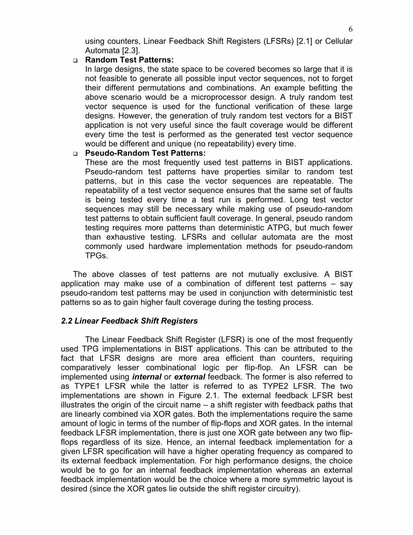
The Linear Feedback Shift Register (LFSR) is one of the most frequently used TPG implementations in BIST applications. This can be attributed to the fact that LFSR designs are more area efficient than counters, requiring comparatively lesser combinational logic per flip-flop. An LFSR can be implemented using internal or external feedback. The former is also referred to as TYPE1 LFSR while the latter is referred to as TYPE2 LFSR. The two implementations are shown in Figure 2.1. The external feedback LFSR best illustrates the origin of the circuit name – a shift register with feedback paths that are linearly combined via XOR gates. Both the implementations require the same amount of logic in terms of the number of flip-flops and XOR gates. In the internal feedback LFSR implementation, there is just one XOR gate between any two flip-flops regardless of its size. Hence, an internal feedback implementation for a given LFSR specification will have a higher operating frequency as compared to its external feedback implementation. For high performance designs, the choice would be to go for an internal feedback implementation whereas an external feedback implementation would be the choice where a more symmetric layout is desired (since the XOR gates lie outside the shift register circuitry).
7
Figure 2.1: LFSR Implementations.
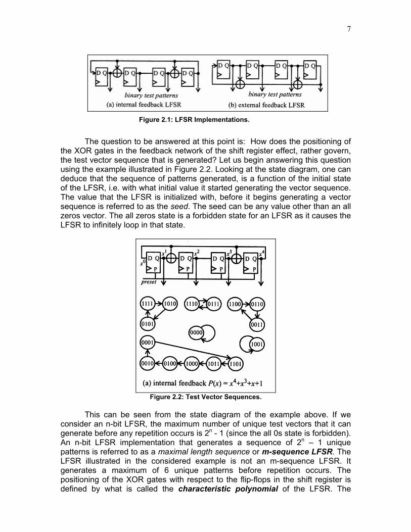
The question to be answered at this point is: How does the positioning of
the XOR gates in the feedback network of the shift register effect, rather govern, the test vector sequence that is generated? Let us begin answering this question using the example illustrated in Figure 2.2. Looking at the state diagram, one can deduce that the sequence of patterns generated, is a function of the initial state of the LFSR, i.e. with what initial value it started generating the vector sequence. The value that the LFSR is initialized with, before it begins generating a vector sequence is referred to as the seed. The seed can be any value other than an all zeros vector. The all zeros state is a forbidden state for an LFSR as it causes the LFSR to infinitely loop in that state.
Figure 2.2: Test Vector Sequences.
This can be seen from the state diagram of the example above. If we
consider an n-bit LFSR, the maximum number of unique test vectors that it can generate before any repetition occurs is 2n - 1 (since the all 0s state is forbidden). An n-bit LFSR implementation that generates a sequence of 2n – 1 unique patterns is referred to as a maximal length sequence or m-sequence LFSR. The LFSR illustrated in the considered example is not an m-sequence LFSR. It generates a maximum of 6 unique patterns before repetition occurs. The positioning of the XOR gates with respect to the flip-flops in the shift register is defined by what is called the characteristic polynomial of the LFSR. The
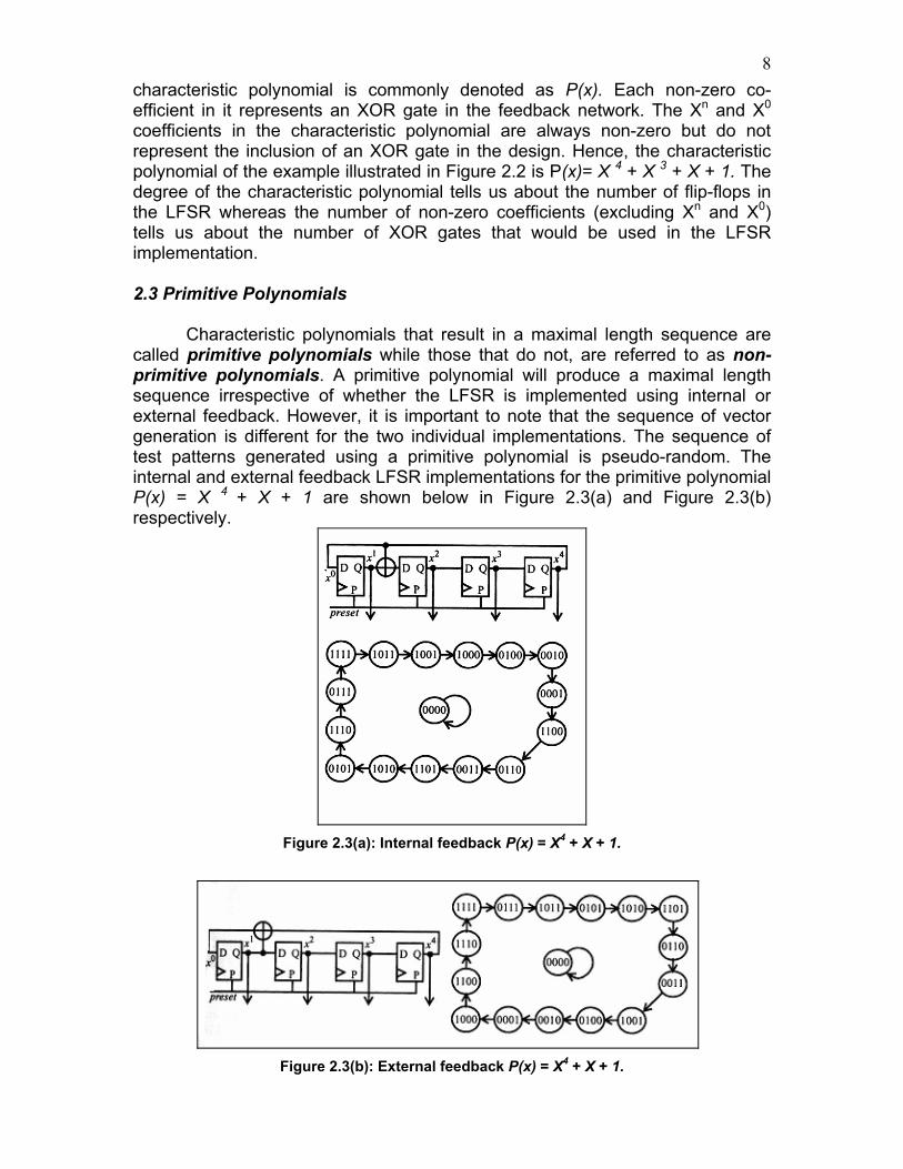
8characteristic polynomial is commonly denoted as P(x). Each non-zero co-efficient in it represents an XOR gate in the feedback network. The Xn and X0 coefficients in the characteristic polynomial are always non-zero but do not represent the inclusion of an XOR gate in the design. Hence, the characteristic polynomial of the example illustrated in Figure 2.2 is P(x)= X 4 + X 3 + X + 1. The degree of the characteristic polynomial tells us about the number of flip-flops in the LFSR whereas the number of non-zero coefficients (excluding Xn and X0) tells us about the number of XOR gates that would be used in the LFSR implementation. 2.3 Primitive Polynomials Characteristic polynomials that result in a maximal length sequence are called primitive polynomials while those that do not, are referred to as non-primitive polynomials. A primitive polynomial will produce a maximal length sequence irrespective of whether the LFSR is implemented using internal or external feedback. However, it is important to note that the sequence of vector generation is different for the two individual implementations. The sequence of test patterns generated using a primitive polynomial is pseudo-random. The internal and external feedback LFSR implementations for the primitive polynomial P(x) = X 4 + X + 1 are shown below in Figure 2.3(a) and Figure 2.3(b) respectively.
Figure 2.3(a): Internal feedback P(x) = X4 + X + 1.
Figure 2.3(b): External feedback P(x) = X4 + X + 1.
9Observe their corresponding state diagrams and note the difference in the
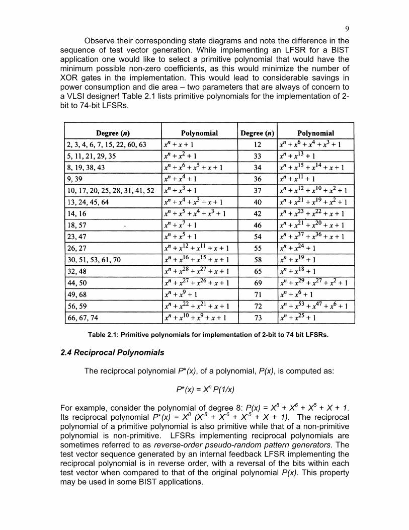
sequence of test vector generation. While implementing an LFSR for a BIST application one would like to select a primitive polynomial that would have the minimum possible non-zero coefficients, as this would minimize the number of XOR gates in the implementation. This would lead to considerable savings in power consumption and die area – two parameters that are always of concern to a VLSI designer! Table 2.1 lists primitive polynomials for the implementation of 2-bit to 74-bit LFSRs.
Table 2.1: Primitive polynomials for implementation of 2-bit to 74 bit LFSRs.
2.4 Reciprocal Polynomials The reciprocal polynomial P*(x), of a polynomial, P(x), is computed as: P*(x) = Xn P(1/x) For example, consider the polynomial of degree 8: P(x) = X8 + X6 + X5 + X + 1. Its reciprocal polynomial P*(x) = X8 (X-8 + X-6 + X-5 + X + 1). The reciprocal polynomial of a primitive polynomial is also primitive while that of a non-primitive polynomial is non-primitive. LFSRs implementing reciprocal polynomials are sometimes referred to as reverse-order pseudo-random pattern generators. The test vector sequence generated by an internal feedback LFSR implementing the reciprocal polynomial is in reverse order, with a reversal of the bits within each test vector when compared to that of the original polynomial P(x). This property may be used in some BIST applications.

102.5 Generic LFSR Design Suppose a BIST application required a certain set of test vector sequences but not all the possible 2n – 1 patterns generated using a given primitive polynomial – this is where a generic LFSR design would find application. Making use of such an implementation would make it possible to reconfigure the LFSR to implement a different primitive/non-primitive polynomial on the fly. A 4-bit generic LFSR implementation making use of both internal and external feedback is shown in Figure 2.4. The control inputs C1, C2 and C3 determine the polynomial implemented by the LFSR. The control input is logic 1 corresponding to each non-zero coefficient of the implemented polynomial.
Figure 2.4: Generic LFSR Implementation.
How do we generate the all zeros pattern?
An LFSR that has been modified for the generation of an all zeros pattern
is commonly termed as a complete feedback shift register (CFSR) since the n-bit LFSR now generates all the 2n possible patterns. For an n-bit LFSR design, additional logic in the form of an (n -1) input NOR gate and a 2 input XOR gate is required. The logic values for all the stages except Xn are logically NORed and the output is XORed with the feedback value. Modified 4-bit LFSR designs are shown in Figure 2.5. The all zeros pattern is generated at the clock event following the 0001 output from the LFSR. The area overhead involved in the generation of the all zeros pattern becomes significant (due to the fan-in limitations for static CMOS gates) for large LFSR implementations considering the fact that just one additional test pattern is being generated. If the LFSR is implemented using internal feedback then performance deteriorates with the number of XOR gates between two flip-flops increasing to two, not to mention the added delay of the NOR gate. An alternate approach would be to increase the LFSR size by one to (n+1) bit(s) so that, at some point in time one can make use of the all zeros pattern available at the n LSB bits of the LFSR output.

11
Figure 2.5: Modified LFSR implementations for the generation of the all zeros pattern 2.6 Weighted LFSRs: Consider a circuit under test (CUT) that incorporates a global reset/preset to its component flip-flops. Frequent resetting of these flip-flops by pseudo-random test vectors will clear the test data propagated into the flip-flops, resulting in the masking of some internal faults. For this reason, the pseudo-random test vector must not cause frequent resetting of the CUT. A solution to this problem would be to create a weighted pseudo-random pattern. For example, one can generate frequent logic 1s by performing a logical NAND of two or more bits or frequent logic 0s by performing a logical NOR of two or more bits of the LFSR. The probability of a given LFSR bit being 0 is 0.5. Hence, performing the logical NAND of three bits will result in a signal whose probability of being 0 is 0.125 (i.e. 0.5 x 0.5 x 0.5). An example of a weighted LFSR design is shown in Figure 2.6 below. If the weighted output was driving an active low global reset signal, then initializing the LFSR to an all 1s state would result in the generation of a global reset signal during the first test vector for initialization of the CUT. Subsequently, this keeps the CUT from getting reset for a considerable amount of time.
Figure 2.6: Weighted LFSR design
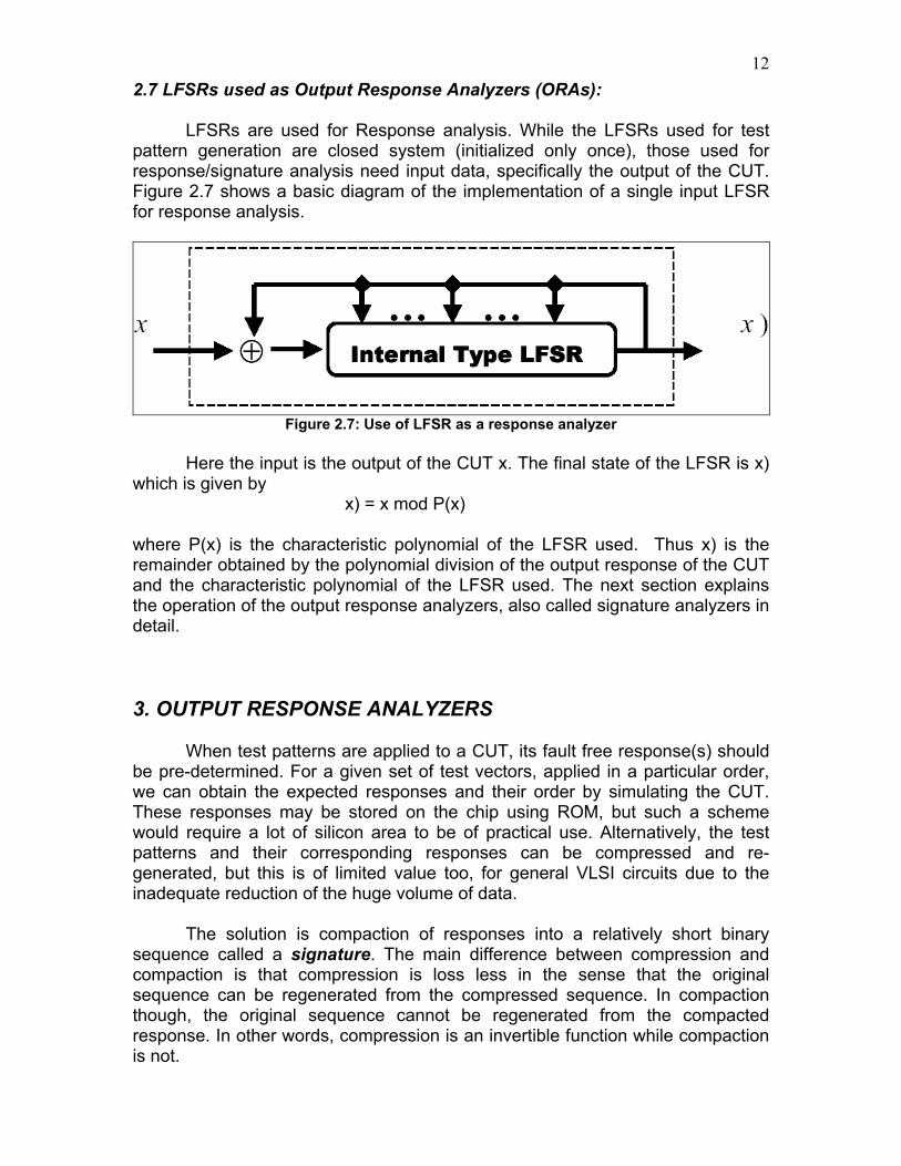
122.7 LFSRs used as Output Response Analyzers (ORAs): LFSRs are used for Response analysis. While the LFSRs used for test pattern generation are closed system (initialized only once), those used for response/signature analysis need input data, specifically the output of the CUT. Figure 2.7 shows a basic diagram of the implementation of a single input LFSR for response analysis.
Figure 2.7: Use of LFSR as a response analyzer Here the input is the output of the CUT x. The final state of the LFSR is x) which is given by x) = x mod P(x) where P(x) is the characteristic polynomial of the LFSR used. Thus x) is the remainder obtained by the polynomial division of the output response of the CUT and the characteristic polynomial of the LFSR used. The next section explains the operation of the output response analyzers, also called signature analyzers in detail. 3. OUTPUT RESPONSE ANALYZERS When test patterns are applied to a CUT, its fault free response(s) should be pre-determined. For a given set of test vectors, applied in a particular order, we can obtain the expected responses and their order by simulating the CUT. These responses may be stored on the chip using ROM, but such a scheme would require a lot of silicon area to be of practical use. Alternatively, the test patterns and their corresponding responses can be compressed and re-generated, but this is of limited value too, for general VLSI circuits due to the inadequate reduction of the huge volume of data. The solution is compaction of responses into a relatively short binary sequence called a signature. The main difference between compression and compaction is that compression is loss less in the sense that the original sequence can be regenerated from the compressed sequence. In compaction though, the original sequence cannot be regenerated from the compacted response. In other words, compression is an invertible function while compaction is not.
133.1 Principle behind ORAs The response sequence R for a given order of test vectors is obtained from a simulator and a compaction function C(R) is defined. The number of bits in C(R) is much lesser than the number in R. These compressed vectors are then stored on or off chip and used during BIST. The same compaction function C is used on the CUTs response R* to provide C(R*). If C(R) and C(R*) are equal, the CUT is declared to be fault-free. For compaction to be practically used, the compaction function C has to be simple enough to implement on a chip, the compressed responses should be small enough and above all, the function C should be able to distinguish between the faulty and fault-free compression responses. Masking [3.3] or aliasing occurs if a faulty circuit gives the same response as the fault-free circuit. Due to the linearity of the LFSRs used, this occurs if and only if the ‘error sequence’ obtained by the XOR operation from the correct and incorrect sequence leads to a zero signature.
Compression can be performed either serially, or in parallel, or in any mixed manner. A purely parallel compression yields a 'global' value C describing the complete behavior of the CUT. On the other hand, if additional information is needed for fault localization then a serial compression technique has to be used. Using such a method, a special compacted value C(R*) is generated for any output response sequence R* where R* depends on the number of output lines of the CUT. 3.2 Different Compression Methods We now take a look at a few of the serial compression methods that are used in the implementation of BIST. Let X=(x1...xt) be a binary sequence. Then, the sequence X can be compressed in the following ways:
3.2.1 Transition counting:
In this method, the signature is the number of 0-to-1 and 1-to-0 transitions in the output data stream. Thus the transition count is given by
t -1 T(X) = ∑(xi ⊕ xi+1) (Hayes, 1976);
i=1 Here the symbol '�' is used to denote the addition modulo 2, but the sum sign must be interpreted by the usual addition.
3.2.2 Syndrome testing (or ones counting):
In this method, a single output is considered and the signature is the number of 1’s appearing in the response R. It is mathematically expressed as:
t Sy(X) = ∑ xi (Savir, 1980);
i=1

143.2.3 Accumulator compression testing:
t k
A(X) = ∑ ∑ xi (Saxena, Robinson1986); k=1 i=1
In each one of these cases, the compaction rate n is of the order of O(log n). The following well-known methods also lead to a constant length of the compressed value.
3.2.4 Parity check compression:
In this method, the compression is performed with the use of a simple LFSR whose primitive polynomial is G(x) = x + 1. The signature S is the parity of the circuit response – it is zero if the parity is even, else it is one. This scheme detects all single and multiple bit errors consisting of an odd number of error bits in the response sequence but fails for a circuit with even number of error bits.
t
P(X) = ⊕ xi i=1
where the bigger symbol '⊕' is used to denote the repeated addition modulo 2.
3.2.5 Cyclic redundancy check (CRC):
A linear feedback shift register of some fixed length n >=1 performs CRC. Here it should be mentioned that the parity test is a special case of the CRC for n = 1.
3.3 Response Analysis: The basic idea behind response analysis is to divide the data polynomial (the input to the LFSR which is essentially the compressed response of the CUT) by the characteristic polynomial of the LFSR. The remainder of this division is the signature used to determine the faulty/fault-free status of the CUT at the end of the BIST sequence. This is illustrated in Figure 3.1 for a 4-bit signature analysis register (SAR) constructed from an internal feedback LFSR with characteristic polynomial from Table 2.1. Since the last bit in the output response of the CUT to enter the SAR denotes the co-efficient x0, the data polynomial of the output response of the CUT can be determined by counting backward from the last bit to the first. Thus the data polynomial for this example is given by K(x), as shown in the Figure 3.3(a). The contents for each clock cycle of the output response from the CUT are shown in Figure 3.3(b) along with the input data K(x), shifting into the SAR on the left hand side and the data shifting out the end of the SAR, Q(x), on the right-hand side. The signature contained in the SAR at the end of the BIST sequence is shown at the bottom of Figure 3.3(b) and is denoted R(x). The polynomial division process is illustrated in Figure 3.3(c) where the division of the CUT output data polynomial, K(x), by the LFSR characteristic polynomial, P(x)
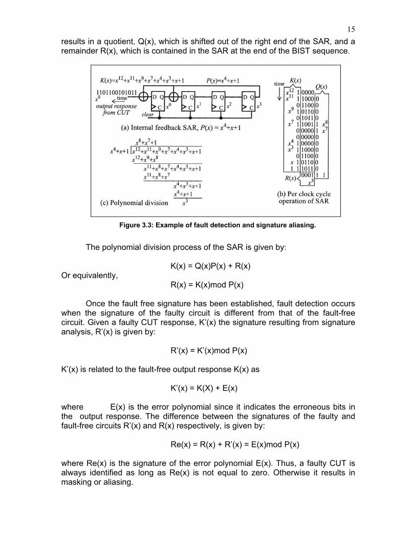
15results in a quotient, Q(x), which is shifted out of the right end of the SAR, and a remainder R(x), which is contained in the SAR at the end of the BIST sequence.
Figure 3.3: Example of fault detection and signature aliasing.
The polynomial division process of the SAR is given by:
K(x) = Q(x)P(x) + R(x) Or equivalently, R(x) = K(x)mod P(x)
Once the fault free signature has been established, fault detection occurs when the signature of the faulty circuit is different from that of the fault-free circuit. Given a faulty CUT response, K’(x) the signature resulting from signature analysis, R’(x) is given by: R’(x) = K’(x)mod P(x) K’(x) is related to the fault-free output response K(x) as K’(x) = K(X) + E(x) where E(x) is the error polynomial since it indicates the erroneous bits in the output response. The difference between the signatures of the faulty and fault-free circuits R’(x) and R(x) respectively, is given by: Re(x) = R(x) + R’(x) = E(x)mod P(x) where Re(x) is the signature of the error polynomial E(x). Thus, a faulty CUT is always identified as long as Re(x) is not equal to zero. Otherwise it results in masking or aliasing.
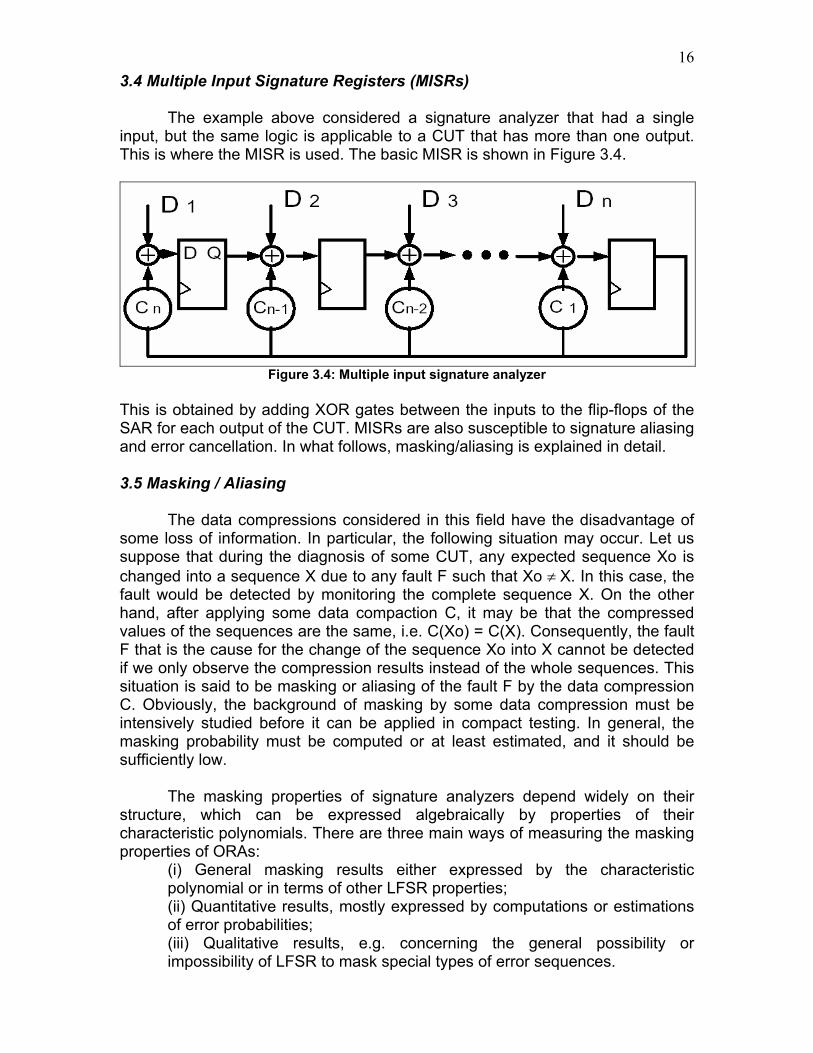
163.4 Multiple Input Signature Registers (MISRs) The example above considered a signature analyzer that had a single input, but the same logic is applicable to a CUT that has more than one output. This is where the MISR is used. The basic MISR is shown in Figure 3.4.
Figure 3.4: Multiple input signature analyzer
This is obtained by adding XOR gates between the inputs to the flip-flops of the SAR for each output of the CUT. MISRs are also susceptible to signature aliasing and error cancellation. In what follows, masking/aliasing is explained in detail. 3.5 Masking / Aliasing The data compressions considered in this field have the disadvantage of some loss of information. In particular, the following situation may occur. Let us suppose that during the diagnosis of some CUT, any expected sequence Xo is changed into a sequence X due to any fault F such that Xo ≠ X. In this case, the fault would be detected by monitoring the complete sequence X. On the other hand, after applying some data compaction C, it may be that the compressed values of the sequences are the same, i.e. C(Xo) = C(X). Consequently, the fault F that is the cause for the change of the sequence Xo into X cannot be detected if we only observe the compression results instead of the whole sequences. This situation is said to be masking or aliasing of the fault F by the data compression C. Obviously, the background of masking by some data compression must be intensively studied before it can be applied in compact testing. In general, the masking probability must be computed or at least estimated, and it should be sufficiently low.
The masking properties of signature analyzers depend widely on their structure, which can be expressed algebraically by properties of their characteristic polynomials. There are three main ways of measuring the masking properties of ORAs:
(i) General masking results either expressed by the characteristic polynomial or in terms of other LFSR properties; (ii) Quantitative results, mostly expressed by computations or estimations of error probabilities; (iii) Qualitative results, e.g. concerning the general possibility or impossibility of LFSR to mask special types of error sequences.
17
The first one includes more general masking results, which are based either on the characteristic polynomial or on other ORA properties. The simulation of the circuit and the compression technique to determine which faults are detected can achieve this. This method is computationally expensive because it involves exhaustive simulation. Smith’s theorem states the same point as:
Any error sequence E=(e1,...,et) is masked by an ORA S if and only if its “error polynomial” pE(x) = e1xt-1+...+et-1x+et is divisible by the characteristic polynomial pS(x) [4].
The second direction in masking studies, which is represented in most of the papers [7],[8] concerning masking problems, can be characterized by “quantitative” results mostly expressed by some computations or estimations of masking probabilities. This is usually not possible and all possible outputs are assumed to be equally probable. But this assumption does not allow one to correlate the probability of obtaining an erroneous signature with fault coverage and hence leads to a rather low estimation of faults. This can be expressed as an extension of Smith’s theorem as:
If we suppose that all error sequences having any fixed length are equally likely the masking probability of any n-stage ORA is not greater than 2-n.
The third direction in studies on masking contains “qualitative” results concerning the general possibility or impossibility of ORAs to mask error sequences of some special type. Examples of such a type are burst errors, or sequences with fixed error-sensitive positions. Traditionally, error sequences having some fixed weight are also regarded as such a special type, where the weight w(E) of some binary sequence E is simply its number of ones. Masking properties for such sequences are studied without restriction of their length. In other words,
If the ORA S is non-trivial then masking of error sequences having the weight 1 by S is impossible.
4. DELAY FAULT TESTING 4.1 Delay Faults Delay faults are failures that cause logic circuits to violate timing specifications. As more aggressive clocking strategies are adopted in sequential circuits, delay faults are becoming more prevalent. Industry has set a trend of pushing clock rates to the limit. Defects that had previously caused minute delays are now causing massive timing failures. The ability to diagnose these faults is essential for improving the yields and quality of integrated circuits. Historically, direct probing techniques such as E-Beam probing have been found to be useful in diagnosing circuit failures. Such techniques, however, are limited by factors such as complicated packaging, long test lengths, multiple metal
18layers, and an ever growing search space that is perpetuated by ever-decreasing device size. 4.2 Delay Fault Models
In this section, we will explore the advantages and limitations of three delay fault models. Other delay fault models exist; but they are essentially derivatives of these three classical models. 4.2.1 Gate Delay
The gate delay model assumes that the delays through logic gates can be accurately characterized. It also assumes that the size and location of probable delay faults is known. Faults are modeled as additive offsets to the propagation of a rising or falling transition from the inputs to the gate outputs. In this scenario, faults retain quantitative values. A delay fault of 200 picoseconds, for example, is not the same as a delay fault of 400 picoseconds using this model.
Research efforts are currently attempting to devise a method to prove that a test will detect any fault at a particular site with magnitude greater than a minimum fault size at a fault site. Certain methods have been proposed for determining the fault sizes detected by a particular test, but are beyond the scope of this discussion. 4.2.2 Transition
A transition fault model classifies faults into two categories: slow-to-rise, and slow-to-fall. It is easy to see how these classifications can be abstracted to a stuck-at-fault model. A slow-to-rise fault would correspond to a stuck-at-zero fault, and a slow-to-fall fault would is synonymous to a stuck-at-one fault. These categories are used to describe defects that delay the rising or falling transition of a gate’s inputs and outputs.
A test for a transition fault is comprised of an initialization pattern and a propagation pattern. The initialization pattern sets up the initial state for the transition. The propagation pattern is identical to the stuck-at-fault pattern of the corresponding fault.
There are several drawbacks to the transition fault model. Its principal weakness is the assumption of a large gate delay. Often, multiple gate delay faults that are undetectable as transition faults can give rise to a large path delay fault. This delay distribution over circuit elements limits the usefulness of transition fault modeling. It is also difficult to determine the minimum size of a detectable delay fault with this model. 4.2.3 Path Delay
The path delay model has received more attention than gate delay and transition fault models. Any path with a total delay exceeding the system clock

19interval is said to have a path delay fault. This model accounts for the distributed delays that were neglected in the transition fault model. Each path that connects the circuit inputs to the outputs has two delay paths. The rising path is the path traversed by a rising transition on the input of the path. Similarly, the falling path is the path traversed by a falling transition on the input of the path. These transitions change direction whenever the paths pass through an inverting gate. Below are three standard definitions that are used in path delay fault testing:
Definition 1: Let G be a gate on path P in a logic circuit, and let r be an input to gate G; r is called an off-path sensitizing input if r is not on path P.
Definition 2: A two-pattern test < VI, V2 > is called a robust test for a delay fault on path P, if the test detects that fault independently of all other delays in the circuit.
Definition 3: A two-pattern test < VI, V2 > is called a non-robust test for a delay fault on path P, if it detects the fault under the assumption that no other path in the circuit involving the off-path inputs of gates on P has a delay fault.
4.3 Delay Faults and BIST
Deriving tests for each of the delay fault models described in the previous section consists of a sequence of two test patterns. This first pattern is denoted as the initialization vector. The propagation vector follows it. Deriving these two pattern tests is know to be NP-hard. Even though test pattern generators exist for these fault models, the cost of high speed Automatic Test Equipment (ATE) and the encapsulation of signals generally prevent these vectors from being applied directly to the CUT. BIST offers a solution to the aforementioned problems.
Sequential circuit testing is complicated by the inability to probe signals internal to the circuit. Scan methods have been widely accepted as a means to externalize these signals for testing purposes. Scan chains, in their simplest form, are sequences of multiplexed flip-flops that can function in normal or test modes. Aside from a slight increase in die area and delay, scannable flip-flops are no different from normal flip-flops when not operating in test mode. The contents of scannable flip-flops that do not have external inputs or outputs can be externally loaded or examined by placing the flip-flops in test mode. Scan methods have proven to be very effective in testing for stuck-at-faults.

20
Figure 4.1: Scan-BIST flowchart
Scan-based BIST is a relatively new testing approach that combines the BIST structure with a scan-based design to provide an efficient means for testing delay faults. The fact that the BIST module can be built around a pre-existing scan chain means that designers do not have to sacrifice the ability to test stuck-at-faults for capability to test delay faults. This is a huge benefit as industry is pushing harder and harder to manufacture circuits that are designed for a higher level of testability.
Figure 4.2: A scan-BIST TPG (a) and its associated subsequence (b).
Scan-based BIST utilizes a novel test pattern generator (TPG). As shown in Figure 4.2(a), the scan-BIST TPG combines outputs from a random pattern generator (RPG) and a scan shift register (SSR) through Ni XOR gates – where Ni is the number of primary inputs on the CUT. The TPG operates as follows: First, the SSR is initialized to a value of (10..0). This pattern creates a walking 1 through the SSR. For each random pattern that is generated, all single input changes (SIC) are produced on the output of the XORs. Figure 4.2(b) shows how the walking 1 generates SIC (low-to-high and high-to-low) transitions for each bit in the random test vector V. SIC vectors have been show to provide very robust testing of path delay faults. One drawback of using scan-based BIST for testing delay faults is a fairly large overhead due to the large size SSRs. Table 4.1 demonstrates the significant increase in fault coverage and area of scan-BIST over pure scan techniques [11].

21
Table 4.1: Comparison of Pure Scan and Scan-BIST
5. NON-INTRUSIVE BIST
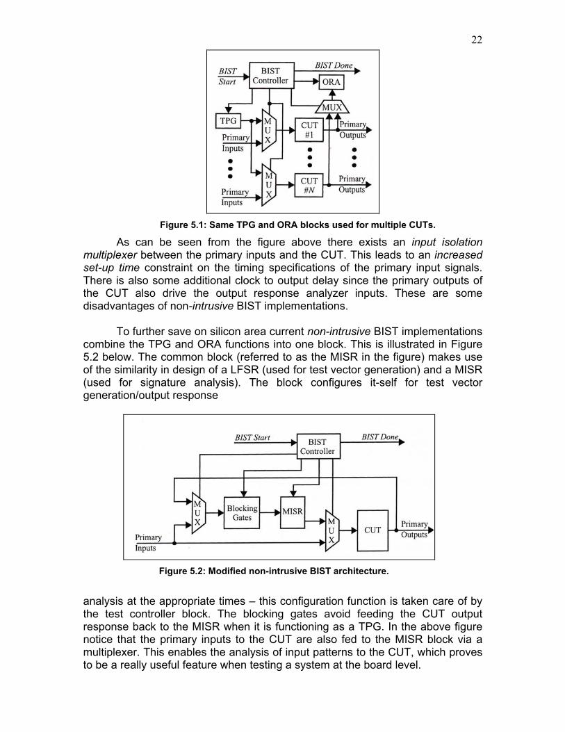
So as to save on silicon area BIST designs make use of existing flip-flops, used to implement the CUT design, to create the test pattern generator and response analyzer functions. In the case of scan based BIST, points of controllability and abservability for the application of test vectors and the capture of the output responses are realized by adding some additional logic in the combinational path between two flip-flops. As a result of this some amount of a performance penalty is incurred since the CUT now operates at a lower clock frequency when compared to a CUT not implementing BIST. Such a BIST implementation is said to be intrusive since it interferes with/affects the operation of the CUT. The basic BIST architecture shown in Figure1 (in the introduction) is an illustration of non-intrusive BIST. Here, the BIST circuitry is separate from the CUT and hence does not impose any performance penalties. As a result non-intrusive BIST implementations are preferred for high performance applications. Since the test pattern generator (TPG) and output response analyzer (ORA) functions are external to the CUT design, they can be used to test multiple CUT blocks (each of the multiple CUT blocks may have a different functionality). This concept is illustrated in Figure 5.1 below. This approach leads to major savings in terms of silicon area.
22
Figure 5.1: Same TPG and ORA blocks used for multiple CUTs.
As can be seen from the figure above there exists an input isolation multiplexer between the primary inputs and the CUT. This leads to an increased set-up time constraint on the timing specifications of the primary input signals. There is also some additional clock to output delay since the primary outputs of the CUT also drive the output response analyzer inputs. These are some disadvantages of non-intrusive BIST implementations. To further save on silicon area current non-intrusive BIST implementations combine the TPG and ORA functions into one block. This is illustrated in Figure 5.2 below. The common block (referred to as the MISR in the figure) makes use of the similarity in design of a LFSR (used for test vector generation) and a MISR (used for signature analysis). The block configures it-self for test vector generation/output response
Figure 5.2: Modified non-intrusive BIST architecture.
analysis at the appropriate times – this configuration function is taken care of by the test controller block. The blocking gates avoid feeding the CUT output response back to the MISR when it is functioning as a TPG. In the above figure notice that the primary inputs to the CUT are also fed to the MISR block via a multiplexer. This enables the analysis of input patterns to the CUT, which proves to be a really useful feature when testing a system at the board level.

23
6. APPENDIX
6.1 AN OVERVIEW OF DIFFERENT FAULT MODELS
A good fault model accurately reflects the behavior of the actual defects that can occur during the fabrication and manufacturing processes, as well as the behavior of the faults that can occur during system operation. A brief description of the different fault models in use is presented here:
Gate-Level Single Stuck-At Fault Model: The gate-level stuck-at fault
model emulates the condition where the input/output terminal of a logic gate is stuck-at logic0 level (s-a-0) or logic level 1 (s-a-1). On a gate-level logic diagram the presence of a stuck-at fault is denoted by placing a cross (denoted as ‘x’) at the fault site, along with an s-a-0 or s-a-1 label describing the type of fault. This is illustrated in Figure1 below. The single stuck-at fault model assumes that at a given point in time only as single stuck-at fault exists in the logic circuit being analyzed. This is an important assumption that must be borne in mind when making use of this fault model. Each of the inputs and outputs of logic gates serve as potential fault sites, with the possibility of either an s-a-0 or an s-a-1 fault occurring at those locations. Figure1 shows how the occurrences of the different possible stuck-at faults impact the operational behavior of some basic gates.
Figure1: Gate-Level Stuck-at Fault behavior.
At this point a question may arise in our minds – what could cause the input/output of a logic gate to be stuck-at logic 0 or stuck-at logic1? This could happen as a result of a faulty fabrication process, where the input/output of a logic gate is accidentally routed to power (logic1) or ground (logic0).

24
Transistor-Level single Stuck Fault Model: Here the level of fault emulation drops down to the transistor level implementation of logic gates used to implement the design. The transistor-level stuck model assumes that a transistor can be faulty in two ways – the transistor is permanently ON (referred to as stuck-on or stuck-short) or the transistor is permanently OFF (referred to as stuck-off or stuck-open). The stuck-on fault is emulated by shorting the source and drain terminals of the transistor (assuming a static CMOS implementation) in the transistor level circuit diagram of the logic circuit. A stuck-off fault is emulated by disconnecting the transistor from the circuit. A stuck-on fault could also be modeled by tying the gate terminal of the pMOS/nMOS transistor to logic0/logic1 respectively. Similarly, tying the gate terminal of the pMOS/nMOS transistor to logic1/logic0 respectively would simulate a stuck-off fault. Figure2 below illustrates the effect of transistor-level stuck faults on a two-input NOR gate.
Figure2: Transistor-level Stuck Fault model and behavior.
It is assumed that only a single transistor is faulty at a given point in time. In the case of transistor stuck-on faults some input patterns could produce a conducting path from power to ground. In such a scenario the voltage level at the output node would be neither logic0 nor logic1, but would be a function of the voltage divider formed by the effective channel resistances of the pull-up and the pull-down transistor stacks. Hence, for the example illustrated in Figure2, when the transistor corresponding to the A input is stuck-on, the output node voltage level Vz would be computed as:
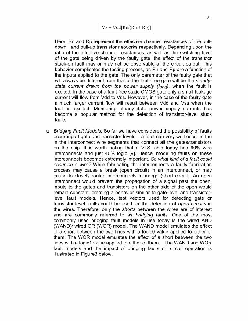
25
Here, Rn and Rp repdown and pull-up trratio of the effective of the gate being drstuck-on fault may obehavior complicatesthe inputs applied to will always be differestate current drawnexcited. In the case ocurrent will flow froma much larger currefault is excited. Mobecome a popular faults.
Bridging Fault Modelsoccurring at gate andin the interconnect won the chip. It is wointerconnects and juinterconnects becomeoccur on a wire? Whprocess may cause cause to closely routinterconnect would pinputs to the gates aremain constant, crealevel fault models. transistor-level faults the wires. Therefore,and are commonly commonly used brid(WAND)/ wired OR (Wof a short between ththem. The WOR modlines with a logic1 valfault models and theillustrated in Figure3 b
Vz = Vdd[Rn/(Rn + Rp)]
resent the effective channel resistances of the pull-ansistor networks respectively. Depending upon the channel resistances, as well as the switching level iven by the faulty gate, the effect of the transistor r may not be observable at the circuit output. This the testing process, as Rn and Rp are a function of the gate. The only parameter of the faulty gate that nt from that of the fault-free gate will be the steady- from the power supply (IDDQ), when the fault is f a fault-free static CMOS gate only a small leakage Vdd to Vss. However, in the case of the faulty gate nt flow will result between Vdd and Vss when the nitoring steady-state power supply currents has method for the detection of transistor-level stuck
: So far we have considered the possibility of faults transistor levels – a fault can very well occur in the ire segments that connect all the gates/transistors rth noting that a VLSI chip today has 60% wire
st 40% logic [9]. Hence, modeling faults on these s extremely important. So what kind of a fault could ile fabricating the interconnects a faulty fabrication a break (open circuit) in an interconnect, or may ed interconnects to merge (short circuit). An open revent the propagation of a signal past the open, nd transistors on the other side of the open would ting a behavior similar to gate-level and transistor-
Hence, test vectors used for detecting gate or could be used for the detection of open circuits in only the shorts between the wires are of interest referred to as bridging faults. One of the most ging fault models in use today is the wired AND
OR) model. The WAND model emulates the effect e two lines with a logic0 value applied to either of el emulates the effect of a short between the two
ue applied to either of them. The WAND and WOR impact of bridging faults on circuit operation is elow.

26
Figure3: WAND/ WOR and dominant bridging fault models.
The dominant bridging fault model is yet another popular model used to emulate the occurrence of bridging faults. The dominant bridging fault model accurately reflects the behavior of some shorts in CMOS circuits where the logic value at the destination end of the shorted wires is determined by the source gate with the strongest drive capability. As illustrated in Figure3©, the driver of one node “dominates” the drive of the other node. ”A DOM B” denotes that the driver of node A dominates, as it is stronger than the driver of node B.
Delay Faults: Delay faults are discussed about in detail in Section 4. of this report.
27
7. BIBLIOGRAPHY 1. V D Agrawal, C R Kime and K K Saluja – “A Tutorial on Built-In Self-Test –
Part 1: Principles”, IEEE Design & Test Of Computers, Volume: 10 Issue: 1, March 1993 Page(s): 73 –82.
2. Charles E. Stroud, “A Designer’s Guide to Built-In Self-Test”, Kluwer Academic Publishers, Massachusetts, 2002.
3. V D Agrawal, C R Kime and K K Saluja – “A Tutorial on Built-In Self-Test – Part 2: Applications”, IEEE Design & Test Of Computers, Volume: 10 Issue: 2, June 1993 Page(s): 69 –77.
4. Lutz Voelkel “On the problem of masking special errors by signature analyzers” TR–95–014 April 1995.
5. Abramovici, Miron – “Digital systems testing and testable design”, Piscataway, NJ: IEEE Press, c1990.
6. Bushnell, Michael L – “Essentials of electronic testing for digital, memory, and mixed-signal VLSI circuits”, Boston : Kluwer Academic, c2000. 7. Benowitz,N., Calhoun,D.F., Alderson,G.E., Bauer,J.E., Joeckel,C.T.: “An
Advanced Fault Isolation System for Digital Logic”, IEEE Transactions on Comp. C-24/5 (1975), 489-497.
8. Gordon,G.,Nadig,H.: Hexadecimal Signatures Identify Troublespots in Micro processor Systems. Electronics 50/5(1977),89-96.
9. Dr. Erik Brunvand : “CS6710 Lecture Slides on DFT”. 10. Janusz Rajski, Jerzy Tyszer - “Arithmetic Built-In Self-Test for Embedded
Systems”, Prentice-Hall, Inc. ©1998. 11. P. Girard, C. Landrault, V. Moréda, S. Pravossoudovitch, A. Virazel –
“A New Scan-BIST Structure to Test Delay Faults in Sequential Circuits”,1998. http://www.ra.informatik.uni-stuttgart.de/~virazela/etw98.pdf.
ٱٱٱ