Embed Size (px)
Citation preview
Sanjay Kumar et al. 2016, Volume 4 Issue 1 ISSN (Online): 2348-4098 ISSN (Print): 2395-4752
International Journal of Science,Engineering and Technology
An Open Access Journal
© 2016 Sanjay Kumar et al. This is an Open Access article distributed under the terms of the Creative Commons Attribution License (http://creativecommons.org/licenses/by/4.0), which permits unrestricted use, distribution, and reproduction in any medium, provided the original work is properly credited.
Nanoantenna – A Review on Present and Future Perspective 1Sanjay Kumar, 2Sanju Tanwar, 3Sumit Kumar Sharma
Introduction
A nanoantenna is a solar collection device based on rectifying antennas. Nanoantenna is a recent device, so it does not have an old history. It is worthy to mention that the idea of using antennas to collect solar energy was first proposed by Robert L. Bailey in 1972. In 1973, Robert Bailey, along with James C. Fletcher, received a patent for an electromagnetic wave converter. The patented device was similar to modern day nanoantenna devices. Alvin M. Marks received a patent in 1984 for a device explicitly stating the use of sub-micron antennas for the direct conversion of light into electricity.
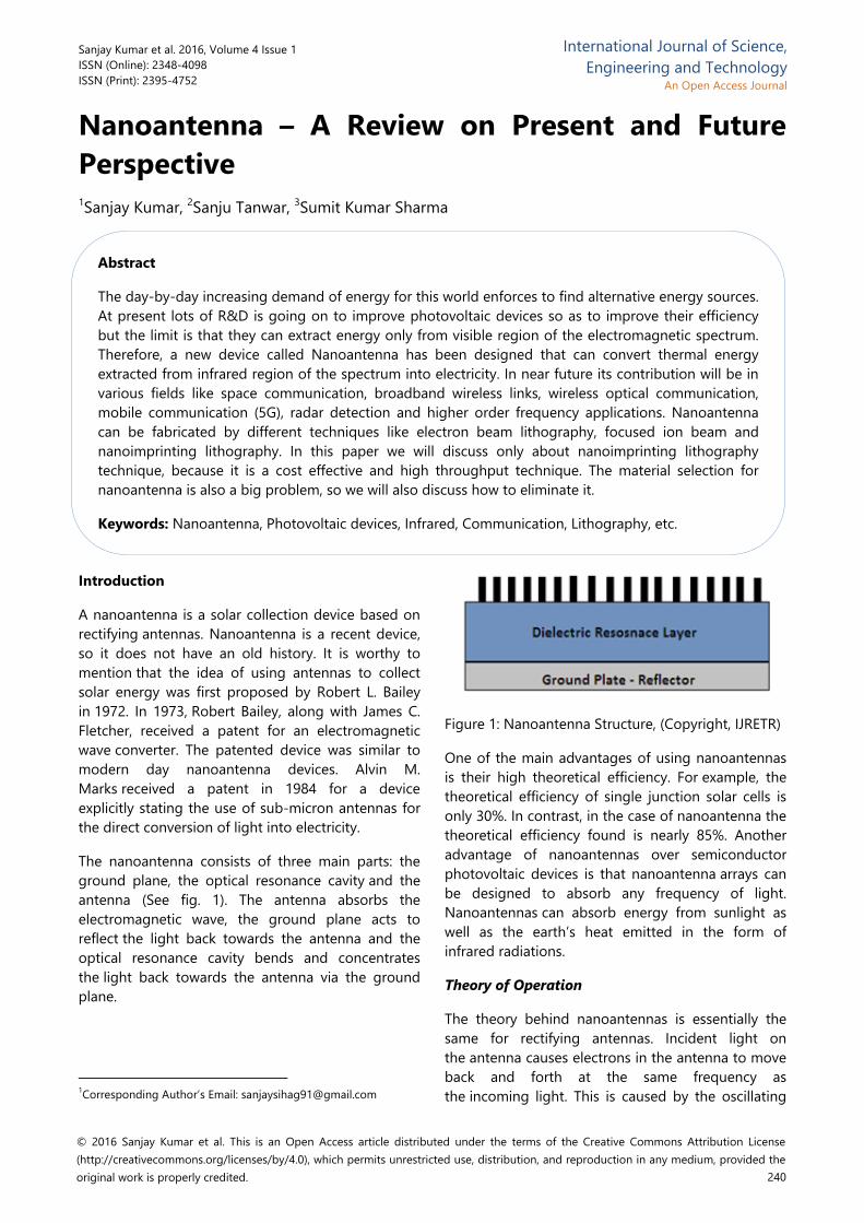
The nanoantenna consists of three main parts: the ground plane, the optical resonance cavity and the antenna (See fig. 1). The antenna absorbs the electromagnetic wave, the ground plane acts to reflect the light back towards the antenna and the optical resonance cavity bends and concentrates the light back towards the antenna via the ground plane.1
1Corresponding Author’s Email: [email protected]
Figure 1: Nanoantenna Structure, (Copyright, IJRETR)
One of the main advantages of using nanoantennas is their high theoretical efficiency. For example, the theoretical efficiency of single junction solar cells is only 30%. In contrast, in the case of nanoantenna the theoretical efficiency found is nearly 85%. Another advantage of nanoantennas over semiconductor photovoltaic devices is that nanoantenna arrays can be designed to absorb any frequency of light. Nanoantennas can absorb energy from sunlight as well as the earth’s heat emitted in the form of infrared radiations.
Theory of Operation
The theory behind nanoantennas is essentially the same for rectifying antennas. Incident light on the antenna causes electrons in the antenna to move back and forth at the same frequency as the incoming light. This is caused by the oscillating
Abstract
The day-by-day increasing demand of energy for this world enforces to find alternative energy sources. At present lots of R&D is going on to improve photovoltaic devices so as to improve their efficiency but the limit is that they can extract energy only from visible region of the electromagnetic spectrum. Therefore, a new device called Nanoantenna has been designed that can convert thermal energy extracted from infrared region of the spectrum into electricity. In near future its contribution will be in various fields like space communication, broadband wireless links, wireless optical communication, mobile communication (5G), radar detection and higher order frequency applications. Nanoantenna can be fabricated by different techniques like electron beam lithography, focused ion beam and nanoimprinting lithography. In this paper we will discuss only about nanoimprinting lithography technique, because it is a cost effective and high throughput technique. The material selection for nanoantenna is also a big problem, so we will also discuss how to eliminate it.
Keywords: Nanoantenna, Photovoltaic devices, Infrared, Communication, Lithography, etc.
240
Sanjay Kumar et al. International Journal of Science, Engineering and Technology, 2016, Volume 4 Issue 1 ISSN (Online): 2348-4098 , ISSN (Print): 2395-4752
electric field of the incoming electromagnetic wave. The movement of electrons is an alternating current in the antenna circuit. To convert this into DC power, the AC current must be rectified, which is typically done with some kind of diode. The resulting DC current can then be used to power an external load.
Fabrication of Nanoantenna
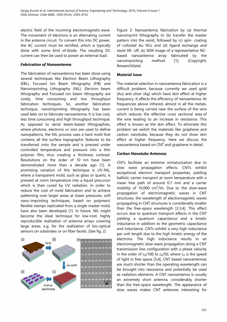
The fabrication of nanoantenna has been done using several techniques like Electron Beam Lithography (EBL), Focused Ion Beam lithography (FIB) and Nanoimprinting Lithography (NIL). Electron beam lithography and Focused ion beam lithography are costly, time consuming and low throughput fabrication techniques. So, another fabrication technique, nanoimprinting lithography has been used later on to fabricate nanoantenna. It is low cost, less time consuming and high throughput technique. As opposed to serial beam-based lithographies, where photons, electrons or ions are used to define nanopatterns, the NIL process uses a hard mold that contains all the surface topographic features to be transferred onto the sample and is pressed under controlled temperature and pressure into a thin polymer film, thus creating a thickness contrast. Resolutions on the order of 10 nm have been demonstrated more than a decade ago [1]. A promising variation of this technique is UV-NIL, where a transparent mold, such as glass or quartz, is pressed at room temperature into a liquid precursor which is then cured by UV radiation. In order to reduce the cost of mold fabrication and to achieve patterning over larger areas at lower pressures, soft nano-imprinting techniques, based on polymeric flexible stamps replicated from a single master mold, have also been developed [1]. In future, NIL might become the ideal technique for low-cost, highly reproducible realization of antenna arrays covering large areas, e.g. for the realization of bio-optical sensors on substrates or on fiber facets. (See fig. 2)
Figure 2: Nanoantenna fabrication by (a) thermal nanoimprint lithography to (b) transfer the master pattern into the resist, followed by (c) spin- coating of colloidal Au NCs and (d) ligand exchange and resist lift- off. (e) SEM image of a representative NC- based nanoantenna array fabricated by the nanoimprinting method [1], (Copyright, ResearchGate)
Material Issue
The material selection in nanoantenna fabrication is a difficult problem, because currently we used gold (Au) and silver (Ag) which have skin effect at higher frequency. It affects the efficiency of nanoantenna. At frequencies above infrared, almost in all the metals, current is being carried near the surface of the wire which reduces the effective cross sectional area of the wire leading to an increase in resistance. This effect is known as the skin effect. To eliminate this problem we switch the materials like graphene and carbon nanotube, because they do not show skin effect at higher frequency. Here we discuss the nanoantenna based on CNT and graphene in detail.
Carbon Nanotube Antennas
CNTs facilitate an extreme miniaturization due to slow wave propagation effects. CNTs exhibit exceptional electron transport properties, yielding ballistic carrier transport at room temperature with a mean free path of around 0.7 mm and a carrier mobility of 10,000 cm2/Vs. Due to the slow-wave propagation of electromagnetic waves in CNT structures, the wavelength of electromagnetic waves propagating in CNT structures is considerably smaller than the free-space wavelength [2,3,4]. This effect occurs due to quantum transport effects in the CNT yielding a quantum capacitance and a kinetic inductance in addition to the geometric capacitance and inductance. CNTs exhibit a very high inductance per unit length due to the high kinetic energy of the electrons. The high inductance results in an electromagnetic slow-wave propagation along a CNT transmission line configuration with a phase velocity in the order of c0/100 to c0/50, where c0 is the speed of light in free space [3,4]. CNT based nanoantennas are much shorter than the operating wavelength can be brought into resonance and potentially be used as radiation elements. A CNT nanoantenna is usually an extremely short antenna, considerably shorter than the free-space wavelength. The appearance of slow waves makes CNT antennas interesting for
241
Sanjay Kumar et al. International Journal of Science, Engineering and Technology, 2016, Volume 4 Issue 1 ISSN (Online): 2348-4098 , ISSN (Print): 2395-4752
wireless communication between circuits at the micro and nanoscale.
Copper and carbon dipole nanoantennas are investigated using modified Hallén and Pockling ton integral equations, which incorporate the CNT surface conductance. It was found that CNT dipoles start to go into resonance at much lower frequencies than initially assumed. This can be explained from the fact that electromagnetic waves are propagating along CNTs, forming surface plasmons, which have are induced propagation velocity and thus have shorter wavelengths. So, CNT dipoles with several micrometer sin length starts to resonate in the low terahertz region, where the wavelengths are 50–100 times larger compared to the length of the CNT dipole [5, 6].
Linear nanoscale dipole antennas either made of metal such as gold or silver or CNTs have been investigated. Due to the extremely high aspect ratio (length/cross sectional area), both metal nanowires as well as CNTs have AC resistances per unit length in the order of several kilo-ohm per micrometer. This high resistance causes high conduction losses and thus seriously decreases the efficiency and the achievable gain of nanoantennas. The efficiency of a CNT dipole antenna is estimated to being the range of –60 to –90 dB, which results from the high conductance losses. The situation in the case of metal nanoantennas is similar. Although low power levels are sufficient in modern communication links, the inherent loss introduced by metallic or CNT nanoantennas limits their applicability considerably. One approach to bypass the resistance problem could be the usage of arrays of nanoantennas or a bundle of parallel nanowires. In this case, the resistance can be decreased to an acceptable value; however, the slow wave effect is lost, as discussed in. Therefore, by an appropriate choice of geometry and the number of nanowires, the properties of nanoantenna structures have to be optimized.
Graphene Antennas
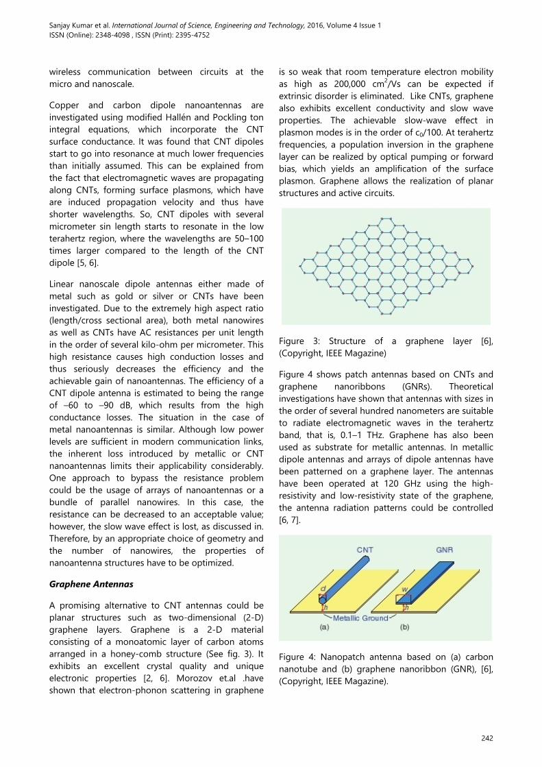
A promising alternative to CNT antennas could be planar structures such as two-dimensional (2-D) graphene layers. Graphene is a 2-D material consisting of a monoatomic layer of carbon atoms arranged in a honey-comb structure (See fig. 3). It exhibits an excellent crystal quality and unique electronic properties [2, 6]. Morozov et.al .have shown that electron-phonon scattering in graphene
is so weak that room temperature electron mobility as high as 200,000 cm2/Vs can be expected if extrinsic disorder is eliminated. Like CNTs, graphene also exhibits excellent conductivity and slow wave properties. The achievable slow-wave effect in plasmon modes is in the order of c0/100. At terahertz frequencies, a population inversion in the graphene layer can be realized by optical pumping or forward bias, which yields an amplification of the surface plasmon. Graphene allows the realization of planar structures and active circuits.
Figure 3: Structure of a graphene layer [6], (Copyright, IEEE Magazine)
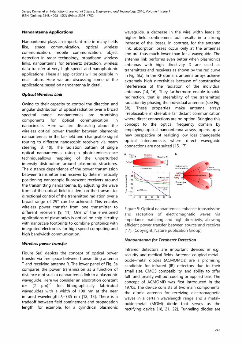
Figure 4 shows patch antennas based on CNTs and graphene nanoribbons (GNRs). Theoretical investigations have shown that antennas with sizes in the order of several hundred nanometers are suitable to radiate electromagnetic waves in the terahertz band, that is, 0.1–1 THz. Graphene has also been used as substrate for metallic antennas. In metallic dipole antennas and arrays of dipole antennas have been patterned on a graphene layer. The antennas have been operated at 120 GHz using the high-resistivity and low-resistivity state of the graphene, the antenna radiation patterns could be controlled [6, 7].
Figure 4: Nanopatch antenna based on (a) carbon nanotube and (b) graphene nanoribbon (GNR), [6], (Copyright, IEEE Magazine).
242
Sanjay Kumar et al. International Journal of Science, Engineering and Technology, 2016, Volume 4 Issue 1 ISSN (Online): 2348-4098 , ISSN (Print): 2395-4752
Nanoantenna Applications
Nanoantenna plays an important role in many fields like, space communication, optical wireless communication, mobile communication, object detection in radar technology, broadband wireless links, nanoantenna for terahertz detection, wireless data transfer at very high speed, and nanophotonic applications. These all applications will be possible in near future. Here we are discussing some of the applications based on nanoantenna in detail.
Optical Wireless Link
Owing to their capacity to control the direction and angular distribution of optical radiation over a broad spectral range, nanoantennas are promising components for optical communication in nanocircuits. Here we are discussing about the wireless optical power transfer between plasmonic nanoantennas in the far-field and changeable signal routing to different nanoscopic receivers via beam steering [8, 10]. The radiation pattern of single optical nanoantennas using a photoluminescence techniqueallows mapping of the unperturbed intensity distribution around plasmonic structures. The distance dependence of the power transmission between transmitter and receiver by deterministically positioning nanoscopic fluorescent receivers around the transmitting nanoantenna. By adjusting the wave front of the optical field incident on the transmitter directional control of the transmitted radiation over a broad range of 29° can be achieved. This enables wireless power transfer from one transmitter to different receivers [9, 11]. One of the envisioned applications of plasmonics is optical on chip circuitry with nanoscale footprints to combine photonics with integrated electronics for high speed computing and high bandwidth communication.
Wireless power transfer
Figure 5(a) depicts the concept of optical power transfer via free space between transmitting antenna T and receiving antenna R. The lower panel of Fig. 5a compares the power transmission as a function of distance d of such a nanoantenna link to a plasmonic waveguide. Here we consider an absorption constant α= (2 μm)−1 for lithographically fabricated waveguides with a width of 100 nm at the near infrared wavelength λ=785 nm [12, 13]. There is a tradeoff between field confinement and propagation length, for example, for a cylindrical plasmonic
waveguide, a decrease in the wire width leads to higher field confinement but results in a strong increase of the losses. In contrast, for the antenna link, absorption losses occur only at the antennas and are thus much lower than for a waveguide. The antenna link performs even better when plasmonics antennas with high directivity D are used as transmitters and receivers as shown by the red curve in Fig. 5(a). In the RF domain, antenna arrays achieve extremely high directivities because of constructive interference of the radiation of the individual antennas [14, 16]. They furthermore enable tunable redirection, that is, steerability of the transmitted radiation by phasing the individual antennas (see Fig. 5b). These properties make antenna arrays irreplaceable in steerable far distant communication where direct connections are no option. Bringing this concept to the optical frequency domain by employing optical nanoantenna arrays, opens up a new perspective of realizing low loss changeable optical interconnects where direct waveguide connections are not suited [15, 17].
Figure 5: Optical nanoantennas enhance transmission and reception of electromagnetic waves via impedance matching and high directivity, allowing efficient power transfer between source and receiver [17], (Copyright, Nature publication Group).
Nanoantenna for Terahertz Detection
Infrared detectors are important devices in e.g., security and medical fields. Antenna-coupled metal–oxide–metal diodes (ACMOMDs) are a promising candidate for infrared (IR) detectors due to their small size, CMOS compatibility, and ability to offer full functionality without cooling or applied bias. The concept of ACMOMD was first introduced in the 1970s. The device consists of two main components: the dipole antenna for receiving electromagnetic waves in a certain wavelength range and a metal–oxide–metal (MOM) diode that serves as the rectifying device [18, 21, 22]. Tunneling diodes are
243
Sanjay Kumar et al. International Journal of Science, Engineering and Technology, 2016, Volume 4 Issue 1 ISSN (Online): 2348-4098 , ISSN (Print): 2395-4752
promising candidates for the rectification of terahertz signals because of the femtosecond tunneling times of an electron through a thin barrier in a MOM diode. All of the ACMOMDs, fabricated through either the evaporation technique or the two step EBL technique that pass the dc test of showing nonzero curvature coefficient are subjected to IR characterization for full detector functionality. A linearly polarized continuous wave (CW) CO2 laser has been used as the IR source. The shape of the IR beam has been characterized through the knife-edge experiment and the 1/e2 beam width was found to be 4 mm [19, 21]. The laser beam passes through a polarizer, mechanical chopper, and a half-wave plate before it hits the device-under-test, the ACMOMDs. The half-wave plate is used to rotate the polarization of the IR laser without changing the orientation of devices or the laser.
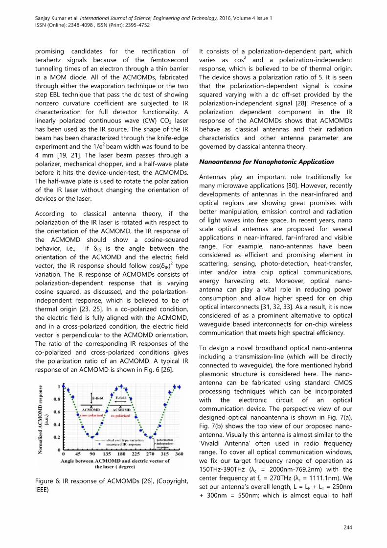
According to classical antenna theory, if the polarization of the IR laser is rotated with respect to the orientation of the ACMOMD, the IR response of the ACMOMD should show a cosine-squared behavior, i.e., if δIR is the angle between the orientation of the ACMOMD and the electric field vector, the IR response should follow cos(δIR)2 type variation. The IR response of ACMOMDs consists of polarization-dependent response that is varying cosine squared, as discussed, and the polarization-independent response, which is believed to be of thermal origin [23. 25]. In a co-polarized condition, the electric field is fully aligned with the ACMOMD, and in a cross-polarized condition, the electric field vector is perpendicular to the ACMOMD orientation. The ratio of the corresponding IR responses of the co-polarized and cross-polarized conditions gives the polarization ratio of an ACMOMD. A typical IR response of an ACMOMD is shown in Fig. 6 [26].
Figure 6: IR response of ACMOMDs [26], (Copyright, IEEE)
It consists of a polarization-dependent part, which varies as cos2 and a polarization-independent response, which is believed to be of thermal origin. The device shows a polarization ratio of 5. It is seen that the polarization-dependent signal is cosine squared varying with a dc off-set provided by the polarization-independent signal [28]. Presence of a polarization dependent component in the IR response of the ACMOMDs shows that ACMOMDs behave as classical antennas and their radiation characteristics and other antenna parameter are governed by classical antenna theory.
Nanoantenna for Nanophotonic Application
Antennas play an important role traditionally for many microwave applications [30]. However, recently developments of antennas in the near-infrared and optical regions are showing great promises with better manipulation, emission control and radiation of light waves into free space. In recent years, nano scale optical antennas are proposed for several applications in near-infrared, far-infrared and visible range. For example, nano-antennas have been considered as efficient and promising element in scattering, sensing, photo-detection, heat-transfer, inter and/or intra chip optical communications, energy harvesting etc. Moreover, optical nano-antenna can play a vital role in reducing power consumption and allow higher speed for on chip optical interconnects [31, 32, 33]. As a result, it is now considered of as a prominent alternative to optical waveguide based interconnects for on-chip wireless communication that meets high spectral efficiency.
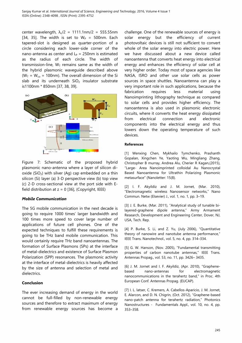
To design a novel broadband optical nano-antenna including a transmission-line (which will be directly connected to waveguide), the fore mentioned hybrid plasmonic structure is considered here. The nano-antenna can be fabricated using standard CMOS processing techniques which can be incorporated with the electronic circuit of an optical communication device. The perspective view of our designed optical nanoantenna is shown in Fig. 7(a). Fig. 7(b) shows the top view of our proposed nano-antenna. Visually this antenna is almost similar to the ‘Vivaldi Antenna’ often used in radio frequency range. To cover all optical communication windows, we fix our target frequency range of operation as 150THz-390THz (λc = 2000nm-769.2nm) with the center frequency at fc = 270THz (λc = 1111.1nm). We set our antenna’s overall length, L = LP + LT = 250nm + 300nm = 550nm; which is almost equal to half
244
Sanjay Kumar et al. International Journal of Science, Engineering and Technology, 2016, Volume 4 Issue 1 ISSN (Online): 2348-4098 , ISSN (Print): 2395-4752
center wavelength, λc/2 = 1111.1nm/2 = 555.55nm [34, 35]. The width is set to WP = 500nm. Each tapered-slot is designed as quarter-portion of a circle considering each lower-side corner of the nano-antenna as center and LP = 250nm is estimated as the radius of each circle. The width of transmission-line, WT remains same as the width of the hybrid plasmonic waveguide described above (WT = Wco = 100nm). The overall dimension of the Si slab and its underneath SiO2 insulator substrate is1100nm * 850nm [37, 38, 39].
Figure 7: Schematic of the proposed hybrid plasmonic nano-antenna where a layer of silicon di-oxide (SiO2) with silver (Ag) cap embedded on a thin silicon (Si) layer (a) 3-D perspective view (b) top view (c) 2-D cross-sectional view at the port side with E-field distribution at z = 0 [36], (Copyright, IEEE)
Mobile Communication
The 5G mobile communication in the next decade is going to require 1000 times’ larger bandwidth and 100 times more speed to cover large number of applications of future cell phones. One of the expected techniques to fulfill these requirements is going to be THz band mobile communication. This would certainly require THz band nanoantennas. The formation of Surface Plasmons (SPs) at the interface of metal-dielectrics and existence of Surface Plasmon Polarization (SPP) resonances. The plasmonic activity at the interface of metal-dielectrics is heavily affected by the size of antenna and selection of metal and dielectrics.
Conclusion
The ever increasing demand of energy in the world cannot be full-filled by non-renewable energy sources and therefore to extract maximum of energy from renewable energy sources has become a
challenge. One of the renewable sources of energy is solar energy but the efficiency of current photovoltaic devices is still not sufficient to convert whole of the solar energy into electric power. Here we have discussed about a new device called nanoantenna that converts heat energy into electrical energy and enhances the efficiency of solar cell at very higher order. Today most of space agencies like NASA, ISRO and other use solar cells as power sources in space shuttles. Nanoantenna can play a very important role in such applications, because the fabrication requires less material using Nanoimprinting lithography technique as compared to solar cells and provides higher efficiency. The nanoantenna is also used in plasmonic electronic circuits, where it converts the heat energy dissipated from electrical connection and electronic components into the electrical energy and thus lowers down the operating temperature of such devices.
References
[1] Wenxing Chen, Mykhailo Tymchenko, Prashanth Gopalan, Xingchen Ye, Yaoting Wu, Mingliang Zhang, Christopher B murray, Andrea Alu, Cherier R Kagan,(2015), “Large- Area Nanoimprinted colloidal Au Nanocrystal Based Nanoantenna for Ultrathin Polarizing Plasmonic metasurface” (Nanoletter: 15(8).
[2] I. F. Akyildiz and J. M. Jornet, (Mar. 2010), “Electromagnetic wireless Nanosensor networks,” Nano Commun. Netw (Elsevier) J., vol. 1, no. 1, pp. 3–19.
[3] J. E. Burke, (Mar. 2011), “Analytical study of tunable bi-layered-graphene dipole antenna,” Army Armament Research, Development and Engineering Center, Dover, NJ, USA, Tech. Rep.
[4] P. Burke, S. Li, and Z. Yu, (July 2006), “Quantitative theory of nanowire and nanotube antenna performance,” IEEE Trans. Nanotechnol., vol. 5, no. 4, pp. 314–334.
[5] G. W. Hanson, (Nov. 2005), “Fundamental transmitting properties of carbon nanotube antennas,” IEEE Trans. Antennas Propag., vol. 53, no. 11, pp. 3426– 3435.
[6] J. M. Jornet and I. F. Akyildiz, (Apr. 2010), “Graphene-based nano-antennas for electromagnetic nanocommunications in the terahertz band,” in Proc. 4th European Conf. Antennas Propag. (EUCAP).
[7] I. L. latser, C. Kremers, A. Cabellos-Aparicio, J. M. Jornet, E. Alarcon, and D. N. Chigrin, (Oct. 2012), “Graphene-based nano-patch antenna for terahertz radiation,” Photonics Nanostructures - Fundamentals Appl., vol. 10, no. 4, pp. 353–358.
245
Sanjay Kumar et al. International Journal of Science, Engineering and Technology, 2016, Volume 4 Issue 1 ISSN (Online): 2348-4098 , ISSN (Print): 2395-4752
[8] Alduino, A. & Paniccia, M. (2007), Interconnects: wiring electronics with light. Nat. Photon. 1, 153–155.
[9] Huang, J.S., Feichtner, T., Biagioni, P. & Hecht, B. (2009), Impedance matching and emission properties of nanoantennas in an optical nanocircuit. Nano Lett. 9, 897–902.
[10] Ozbay, E. (2006), Plasmonics: merging photonics and electronics at nanoscale dimensions. Science 311, 189–193.
[11] Maier, S. A. et al. (2003), Local detection of electromagnetic energy transport below the diffraction limit in metal nanoparticle plasmon waveguides. Nat. Mater. 2, 229–232.
[12] Curto, A. G. et al. (2010), Unidirectional emission of a quantum dot coupled to a nanoantenna. Science 329, 930–933.
[13] Kosako, T., Kadoya, Y. & Hofmann, H. F. (2010), Directional control of light by a nanooptical YagiUda antenna. Nat. Photon. 4, 312–315.
[14] Dorf müller, J. et al. (2011), Near field dynamics of optical Yagi Uda nanoantennas. Nano Lett. 11, 2819.
[15] Balanis, C. A. (2005), Antenna Theory John Wiley & Sons.
[16] Dregely, D. et al. (2011), 3D optical Yagi Uda nanoantenna array. Nat. Commun. 2, 267.
[17] Sun, J., Timurdogan, E., Yaacobi, A., Hosseini, E. S. & Watts, (2013), M. R. Large scale nanophotonic phased array. Nature 493, 195–199.
[18] J. A. Bean, B. Tiwari, G. H. Bernstein, P. Fay, and W. Porod, (2009), “Thermal infrared detection using dipole antenna-coupled metal–oxide–metal diodes,” J. Vac. Sci. Technol. B, Microelectron. Nanometer Struct., vol. 27, pp. 11–14.
[19] I. Codreanu, F. J. Gonzalez, and G. D. Boreman, (2003), “Detection mechanisms in microstrip dipole antenna-coupled infrared detectors,” Infrared Phys. Technol., vol. 44, pp. 155–163.
[20] C. Fumeaux, W. Herrmann, H. Rothuizen, P. De Natale, and F. K. Kneubühl, (1996), “Mixing of 30 THz laser radiation with nanometer thin-film Ni–NiO–Ni diodes and integrated bow-tie antennas,” Appl. Phys. B, Lasers Opt., vol. 63, pp. 135–140.
[21] P. Hobbs, R. Laibowitz, and F. Libsch, (2005), “Ni–NiO–Ni tunnel junctions for terahertz and infrared detection,” Appl. Opt., vol. 44, pp. 6813–6822.
[22] M. Heiblum, W. Shihyuan, J. Whinnery, and T. Gustafson, (1978),“Characteristics of integrated MOM
junctions at dc and at optical frequencies,” IEEE J. Quantum Electron., vol. 14, pp. 159–169.
[23] M. Heiblum, S. Y. Wang, T. K. Gustafson, and J. R. Whinnery, (Sept. 1977), “IIb-7 edge-MOM diode: An integrated, optical, non-linear device,” IEEE Trans. Electron. Devices, vol. ED-24, no. 9, pp. 1199.
[24] S. Y. Wang, T. Izawa, and T. K. Gustafson, (1975), “Coupling characteristics of thin-film metal–oxide–metal diodes at 10.6 m,” Appl. Phys. Lett., vol. 27, pp. 481–483.
[25] J. A. Bean, A.Weeks, and G. D. Boreman, (2011), “Performance optimization of antenna-coupled Al/AlOx/Pt tunnel diode infrared detectors,” IEEE J. Quantum Electron., vol. 47, pp. 126–135.
[26] I.Wilke, Y. Opplinger,W. Herrmann, and F. K. Kneubuhl, (1994), “Nanometerthin-film Ni–NiO–Ni diodes for 30 THz radiation,” Appl. Phy. A, vol. 58, pp. 329–341.
[27] C. Fumeaux, W. Herrmann, F. K. Kneubühl, and H. Rothuizen, (1998), “Nanometer thin-film Ni–NiO–Ni diodes for detection and mixing of 30 THz radiation,” Infrared Phys. Technol., vol. 39, pp. 123–183.
[28] C. A. Balanis, (2005), Antenna Theory: Analysis and Design. Hoboken, NJ: Wiley.
[29] L. Novotny, and N. F. van Hulst, (2011), “Antennas for light”, Nat. Photonics, 5(2), 83 - 90.
[30] T. Shegai, S. Chen, V. D. Miljkovic, G. Zengin, P. Johansson, and M. Kall, (2011), “A bimetallic nanoantenna for directional colour routing”, Nat. Commun., 2, 481 - 486.
[31] J. N. Anker, W. P. Hall, O. Lyandres, N. C. Shah, J. Zhao, and R. P.Van Duyne, (2008), “Biosensing with plasmonic nanosensors”, Nat. Mater., 7, 442-453.
[32] L. Tang, S. E. Kocabas, S. Latif, A. K. Okyay, D. Ly-Gagnon, K. C. Saraswat, and D. A. B. Miller, (2008), “Nanometre-Scale germanium photo-detector enhanced by a near-infrared dipole antenna”, Nat. Photon, 2, 226 – 229.
[33] J. A. Schuller, T. Taubner, and M. L. Brongersma, (2009), “Optical antennathermal emitters”, Nat. Photon., 3, 658 - 661.
[34] L. Yousefi, and A. C. Foster, (2012), “Waveguide-fed optical hybrid plasmonicpatch nano-antenna”, Opt. Express, 20(16), 18326 - 18335.
[35] G. N. M.-Silveira, G. S. Wiederhecker, and H. E. H.-Figueroa, (2013), “Dielectric resonator antenna for applications in nanophotonics”, Opt. Express, 21(1), 1234 - 1239.
246
Sanjay Kumar et al. International Journal of Science, Engineering and Technology, 2016, Volume 4 Issue 1 ISSN (Online): 2348-4098 , ISSN (Print): 2395-4752
[36] Y. Yifat, Z. Iluz, D. B.-Lev, M. Eitan, Y. Hanein, A. Boag, and J. Scheuer, (2013), “Optical resonances of bowtie slot antennas and their geometryand material dependence”, Opt. Lett., 38(2), 205 - 207.
[37] E. D. Palik, Handbook of Optical Constants of Solids, (Academic Press,1998).
[38] P. B. Johnson, and R.W. Christy, (1972), “Optical constants of the noble metals”, Phys. Rev. B, 6, 4370 - 4379.
[39] CSTTM Studio Suite–2012 (https://www.cst.com/).
Author’s details 1,3 M.Tech Scholar, Centre of Nanotechnology, Rajasthan Technical University, Rajasthan 324010.
2Assistant Professor, Centre of Nanotechnology, Rajasthan Technical University, Rajasthan 324010.
Copy for Cite this Article- Sanjay Kumar, Sanju Tanwar and Sumit Kumar Sharma, “Nanoantenna – A Review on Present and Future Perspective’, International Journal of Science, Engineering and Technology, Volume 4 Issue 1: 2016, pp. 240- 247.
Submit your manuscript to International Journal of Science, Engineering and Technology and benefit from:
Convenient Online Submissions
Rigorous Peer Review
Open Access: Articles Freely Available Online
High Visibility Within The Field
Inclusion in Academia, Google Scholar and Cite Factor.
247