Embed Size (px)
Citation preview
i
An Investigation of Porphyrin Aggregation Using
Spectroscopic and Microscopic Methods
By
BENJAMIN A. FRIESEN
A dissertation submitted in partial fulfillment of
the requirements for the degree of
DOCTOR OF PHILOSOPHY
WASHINGTON STATE UNIVERSITY
College of Sciences
MAY 2011
© Copyright by BENJAMIN A. FRIESEN, 2011
All Rights Reserved

ii
© Copyright by BENJAMIN A. FRIESEN, 2011
All Rights Reserved
ii
To the Faculty of Washington State University:
The members of the Committee appointed to examine the dissertation of
BENJAMIN A. FRIESEN find it satisfactory and recommend that it be accepted.
Ursula Mazur, Ph.D., Chair
Kerry Hipps, Ph.D.
James Satterlee, Ph.D.

iii
ACKNOWLEDGMENT
I would like to express my gratitude to my advisor Dr. Ursula Mazur for the
opportunity to work in her lab, for providing financial support, and her patient guidance
through the completion of my doctoral degree. I would also like to convey my thanks to
my committee members Dr. K.W. Hipps and Dr. James Satterlee and to Dr. Jeanne
McHale for a profitable collaboration.
I would also like to thank my wife Angela and my daughter Elizabeth. Their love
and support provided much needed encouragement throughout this process.
iv
An Investigation of Porphyrin Aggregation Using
Spectroscopic and Microscopic Methods
Abstract
By Benjamin A. Friesen, Ph.D.
Washington State University
May 2011
Chair: Ursula Mazur
Aggregates of diacid tetrasulfonatophenylporphine (H2(H4TSPP)) exhibit light
harvesting and electron transport capabilities and are therefore promising candidates as
device components. Before these aggregates can be used to construct devices their
structural and electronic properties must be understood. Solution UV-visible and RLS
studies confirmed the formation of H2(H4TSPP) aggregates with increasing solution ionic
strength. Aggregation of H2(H4TSPP) was indicated by the presence of new absorbance
bands in UV-visible spectra and a marked increase in RLS concurrent with the
appearance of the new UV-visible absorbance bands. Both UV-visible and Raman
spectroscopy confirmed the intact deposition of H2(H4TSPP) aggregates on solid
substrates.
The deposited aggregates were imaged by AFM and STM. The AFM and STM
images revealed individual rods with diameters of ~ 30 nm and lengths of hundreds of
v
nanometers. We report for the first time high resolution STM images of H2(H4TSPP) on
Au(111) and HOPG. In addition to aggregates an ordered monolayer of H2(H4TSPP)
monomers was found on HOPG. The well-defined monolayer islands of H2(H4TSPP)
self- assembled on HOPG were studied in ultrahigh vacuum using STM, OMTS, UPS,
and XPS. Unlike meso-tetrakis(4-carboxyphenyl)porphine (Hx(H4TCPP)), the
carboxylate analog, H2(H4TSPP) monolayers are stable on HOPG and can be studied at
room temperature without the addition of a second stabilizing compound. Protonation of
the porphyrin nitrogens in the surface species is confirmed by XPS. High-resolution
STM images of single molecule layers show a well-defined deformation of the porphyrin
ring, as expected with complete protonation of the central nitrogen atoms. OMTS and
UPS were used to identify the HOMO and LUMO of the H2(H4TSPP) monolayer species,
and results are contrasted to those of nickel(II)tetraphenylporphyrin (NiTPP). Current
vs. Voltage (I(V)) curves of single and stacked rods taken by STM are consistent with
conduction in a band formed from the LUMO of H2(H4TSPP). Aggregate I(V) curves
were consistent with N-type semiconductors and showed increasing current rectification
with increasing aggregate thickness. These findings show that H2(H4TSPP) aggregates
can be used as organic semiconductors with tunable current versus voltage
characteristics.
vi
Table of Contents
ACKNOWLEDGMENT.................................................................................................... iii
Abstract .............................................................................................................................. iv
Table of Contents ............................................................................................................... vi
List of Figures .................................................................................................................... ix
List of Tables ................................................................................................................. xxvi
Glossary of Terms ........................................................................................................ xxviii
Chapter 1: Introduction ...................................................................................................1
1.1 Properties and Applications of Porphyrins.................................................................1
1.2 Literature Review of Porphyrin Aggregation.............................................................9
1.2.1 Non-Ionic Porphyrin Aggregates in Solution and at Surfaces ..........................10
1.2.2 Ionic Porphyrin Aggregates in Solution and on Surfaces ..................................11
1.2.3 Aggregates of Tetrasulfonatophenyporphine: ...................................................14
1.3 The Electronic Structure of Porphyrins and Changes upon Aggregation: ...............29
1.3.1 The Electronic Structure of Porphyrins .............................................................29
1.3.2 Exciton Theory of Dimer and Aggregate Formation: .......................................35
Chapter 2: Experimental Techniques ...........................................................................42
2.1 UV-visible and Resonance Light Scattering Spectroscopy......................................42
2.2 X-ray and Ultraviolet Photoelectron Spectroscopy ..................................................48
vii
2.3 Scanning Tunneling Microscopy (STM)..................................................................52
2.4 Atomic Force Microscopy (AFM) ...........................................................................63
2.5 Raman Spectroscopy: ...............................................................................................65
2.6 Helium Ion Microscopy: ..........................................................................................71
2.7 Transmission Electron Microscopy: ........................................................................73
Chapter 3: Experimental Methods ................................................................................75
3.1 Materials, Reagent, and Instrument List ..................................................................75
3.2 Glassware Cleaning Procedure.................................................................................78
3.3 Preparation of Au(111)/mica Substrates ..................................................................79
3.4 Preparation of STM Tips ..........................................................................................82
3.5 Preparation of Unaggregated and Aggregated Porphyrin Solutions ........................85
3.6 Preparation of H2(H4TSPP) Nanorod Solutions Containing Chloroauric Acid .......86
3.7 Preparation and Analysis of STM and AFM Samples .............................................86
3.7.1 SPM Sample Preparation ...................................................................................86
3.7.2 SPM Data Acquisition .......................................................................................88
3.8 Preparation of Raman Samples ................................................................................90
3.9 Preparation of UV-visible and Resonance Light Scattering Samples ......................91
3.10 Preparation and Measurement of XPS and UPS Samples......................................92
3.10.1 UPS and XPS Sample Preparation ..................................................................92
viii
3.10.2 UPS Spectral Acquisition ................................................................................92
3.10.3 XPS Spectral Acquisition ................................................................................93
3.11 Preparation of Helium Microscope Samples ..........................................................94
3.12 Preparation of Transmission Electron Microscopy Samples .................................94
3.13 Optimization of H2(H4TSPP) geometry with Electron Affinity and Ionization
Potential Calculation. .....................................................................................................95
3.14 Fabrication of and Current vs. Voltage Measurements of H2(H4TSPP) Nanorods
Deposited on Interdigitated Electrodes ..........................................................................95
Chapter 4: Results and Discussion ..............................................................................105
4.1 Characterization of Tetrasulfonatophenyl Porphyrin and its Aggregate by UV-
visible and Resonance Light Scattering Spectroscopy .................................................105
4.2 Characterization of H2(H4TSPP) Aggregates by Ambient SPM Studies ...............119
4.2.1 Characterization of H2(H4TSPP) Aggregates by Tapping Mode AFM ...........119
4.2.2 Characterization of H2(H4TSPP) Aggregates by Ambient Scanning Tunneling
Microscopy ...............................................................................................................125
4.3 Characterization of Tetrasulfonatophenyl Porphyrin and its Aggregate by Raman
and Resonance Raman Spectroscopy ...........................................................................175
4.4 X-ray and Ultraviolet Photoelectron Spectroscopy Analysis of TSPP and its
Aggregate .....................................................................................................................186
4.5 Ultra-High Vacuum STM Studies of H2(H4TSPP) Nanorods ................................207
ix
4.5.1 UHV-STM Imaging Studies of H2(H4TSPP) Nanorods ..................................207
4.5.2 UHV-STM Imaging Studies of H2(H4TSPP) Monomers Deposited on HOPG211
4.5.3 UHV-STM Current versus Voltage Studies of H2(H4TSPP) Nanorods and
Monomers.....................................................................................................................224
4.6 Helium Ion Microscopy Studies .............................................................................232
4.7 Transmission Electron Microscopy Studies ...........................................................238
4.8 Nanorod Current vs. Voltage Studies via Interdigitated Electrode ........................239
Chapter 5: Future Work ..................................................................................................244
Chapter 6: Conclusions ................................................................................................246
List of Figures
Figure 1.1 1: Three forms of porphine, free base, diacid, and metallated along with the
nomeclature tracking the poisitions of substituent groups. ......................................... 2
Figure 1.1 2: Crystal structure of a light harvesting complex in Rhodospirillum
molischianum. Green squares are aggregated bacteriochlorophyll a molecules, blue
squares are monomeric bacteriochlorophyll a, and the yellow structures are
carotenoids. image from reference ............................................................................ 7
Figure 1.1 3: Schematic of photon absorption and electron transport among light
harvesting complexs in Rhodospirillum molischianum. image from reference ........ 8
x
Figure 1.2.3 1: Two forms of tetrasulfonatophenyporphine: free base and diacid. .......... 15
Figure 1.2.3 2: Structure of an H2(H4TSPP) dimer. .......................................................... 16
Figure 1.2.3 3: Proposed model of the structure of the H2(H4TSPP) aggregate based on
cryo-electron microscopy from reference 62. Primed quantities refer to the tilting of
individual porphyrins. The sheet is rolled about the C vector to make the tube. ..... 21
Figure 1.2.3 4: Proposed models of the structure of the H2(H4TSPP) aggregate from
reference 103. B is the direction of the magnetic field. The small arrows are
perpendicular to the porphyrin macrocycle. .............................................................. 23
Figure 1.3.1 1: Schematic of Porphine diacid with overlayed ring and the energy levels
predicted by the particle in a ring model. .................................................................. 29
Figure 1.3.1 2: Orbitals and symmetries which constitute the four orbital model. ........... 30
Figure 1.3.1 3: States arising from configuration interactions in a porphryin. ................. 31
Figure 1.3.1 4: Wavefunctions associated with the electronic states of a D4h porphyrin. 32
Figure 1.3.1 5: UV-visible spectrum of H4(H4TSPP)Cl2 in HCl (pH 3.35)...................... 33
Figure 1.3.2 1: Wavefunctions associated with the electronic states of a D4h porphyrin
and its corresponding dimer. ..................................................................................... 36
Figure 1.3.2 2: Energy level diagram of a dimer with parallel transition dipole moments
with allowed (solid) and forbidden (dashed) transitions. .......................................... 37
Figure 1.3.2 3: Energy level diagram of a dimer with in line transition dipole moments
with allowed (solid) and forbidden (dashed) transitions. .......................................... 38
xi
Figure 1.3.2 4: Energy level diagram of a dimer with co-planar transition dipole moments
with allowed (solid) and forbidden (dashed) transitions. .......................................... 39
Figure 1.3.2 5: Diagram of the H2(H4TSPP) dimer with superimposed transition dipole
moments..................................................................................................................... 40
Figure 2.1 1: Electronic structure of a D4h porphyrin. ...................................................... 43
Figure 2.1 2: Diagram of the electronic states of a D4h porphyrin and its dimer with
overlayed electronic transitions to an excited electronic state. ................................. 44
Figure 2.1 3: Diagram of the the electronic states of a D4h porphyrin and its dimer with an
overlayed scattering process. ..................................................................................... 45
Figure 2.1 4: RLS spectra of H2(H4TSPP) monomer (0.74 µM H2(H4TSPP) in 0.75 M
HCl, left) and aggregate (5.9 µM H2(H4TSPP) in 0.75 M HCl, right). ..................... 47
Figure 2.2 1: Diagrams illustrating photoemission from the valence band (left) and core
levels (right) ............................................................................................................... 49
Figure 2.2 2: XPS spectrum of ethyltrifluoroacetate carbon 1s spectrum illustrating the
chemical shifts of the different carbons. image from reference ............................... 50
Figure 2.2 3: UPS Energy diagram of UPS illustrating the energy of the HeI photon and
the work function (Left), and UPS spectrum of HOPG (Right). ............................... 52
Figure 2.3 1: Diagram of a potential box with a finite barrier. ......................................... 54
Figure 2.3 2: Probability distribution of a particle in a box with a finite barrier. ............. 55
xii
Figure 2.3 3: Tip-sample energy diagram where A) no tunneling is allowed, B) tunneling
from tip to sample is allowed, and C) tunneling from sample to tip is allowed. ....... 56
Figure 2.3 4: Diagrams illustrating the two different modes of STM operation; constant
current and constant height. ....................................................................................... 58
Figure 2.3 5: Diagram illustrating the effect of differing conductivites on the path of an
STM tip. ..................................................................................................................... 60
Figure 2.3 6: Tip-sample energy diagrams with the states of an adsorbed molecule under
a positive sample bias (A) and negative sample bias (B). The arrow indicates the
direction of electron flow. ......................................................................................... 61
Figure 2.4 1: Diagram of the principle components of the AFM. .................................... 64
Figure 2.4 2: Diagram depicting tapping mode AFM....................................................... 65
Figure 2.5 1: Diagram of possible scattering events. ........................................................ 67
Figure 2.5 2: Diagram the Raman experiment and definitions of S and P polarization. .. 69
Figure 2.5 3: Diagram of an adsorbed molecule and its image charges. The charges
cancel in the left-hand case and reinforce in the right-hand arrangement. ................ 70
Figure 2.6 1: A schematic of the Helium Ion Microscope. image from reference .......... 72
Figure 2.6 2: A schematic of the Helium Ion Microscope Tip. image from reference 134
................................................................................................................................... 73
xiii
Figure 3.3 1: Diagram of the apparatus and mask used to make Au(111)/mica substrates
(not to scale). ............................................................................................................. 80
Figure 3.3 2: Ambient STM image of the terraced surface morphology of Au(111). ...... 81
Figure 3.4 1: UHV-STM image and I(V) curve of Au(111). This curve was acquired at
(I,V)=(15 pA, 1.6 V). This I(V) curve is an average of 64 curves. .......................... 84
Figure 3.4 2: UHV-STM image and I(V) curve of HOPG. This curve was acquired at
(I,V)=(15 pA, 1.6 V). This I(V) curve is an average of 64 curves. .......................... 84
Figure 3.7.1 1: Photograph of a Au(111)/mica substrate mounted on the spin chuck used
for deposition. ............................................................................................................ 87
Figure 3.7.1 2: UV-visible spectra of 5 µM H2(H4TSPP)/0.75M HCl before and after
refluxing for 10 min. The black spectrum has been shifted up 0.2 absorbance units
for clarity. .................................................................................................................. 88
Figure 3.14 1: Schematic of the electrode to be used in nanorod I(V) experiments. ........ 96
Figure 3.14 2: AFM image of IdE and cross section. ....................................................... 97
Figure 3.14 3: Cross section of IdE showing the electrode gap distance. ........................ 98
Figure 3.14 4: Experimental setup for IdE I(V) experiments. ........................................ 100
Figure 3.14 5: Photograph of the experimental setup for interdigitated electrode I(V)
measurements. ......................................................................................................... 101
xiv
Figure 3.14 6: Photographs of the channels used to connect the breakout box to the
preamp. .................................................................................................................... 102
Figure 3.14 7: Photographs of the electronics boxes used to hold the resistor for
calibration and the electrode. ................................................................................... 102
Figure 3.14 8: Calibration curve for a 1 gigaohm resistor in the experimental setup
described in Figure 3.14 4. ...................................................................................... 103
Figure 4.1 1: UV-visible specta of tetrasulfonatophenyl porphyrin: free base (Red, pH
10.36) diacid (Black, pH 3.35), and an intermediate pH with both free base and
diacid present (Blue, pH 5.27). ................................................................................ 106
Figure 4.1 2: UV-visible spectra of varying concentrations of H4(H4TSPP)Cl2 in 0.75 M
HCl........................................................................................................................... 107
Figure 4.1 3: Graph of absorbance at 490 nm vs. time during nanorod formation. ........ 109
Figure 4.1 4: UV-visible traces demonstrating the reversibility of aggregation: nanorod
solution at pH 0.12 (green), the same solution after rasing the pH to 10.32 (red), and
a reference free base spectrum at pH 10.00 (black). ............................................... 110
Figure 4.1 5: RLS specta of varying concentrations of H4(H4TSPP)Cl2 in 0.75 M HCl. 111
Figure 4.1 6: RLS specta of varying concentrations of H4(H4TSPP)Cl2 in 0.75 M HCl. 112
Figure 4.1 7: Comparison of the scattering intensity of the J- and Q-bands of
H4(H4TSPP)Cl2 in 0.75 M HCl................................................................................ 113
Figure 4.1 8: Deconvoluted UV-visible spectrum of 5.9 µM H4(H4TSPP)Cl2 in 0.75 M
HCl........................................................................................................................... 114
xv
Figure 4.1 9: Plots of the intensities of various UV-visible peaks as a function of total
porphryin concentration. The concentration of HCl for the left graph is 0.75 M, the
right is 0.40 M. ........................................................................................................ 115
Figure 4.1 10: UV-visible spectra of free base (left) and diacid (right) TSPP solution (red)
and solid phase spectra (black). The concentration of both solution spectra is 2.618
µM. The pH‟s of the solutions in the solution phase spectra are 7.53 and 3.35 for the
free base and diacid respectivly. The solid phase spectra are of 50 µM porphyrin
solutions dried on quartz plates. The pH‟s of the solutions used for deposition are
7.65 and 3.73 for the free base and diacid respectivly. ........................................... 117
Figure 4.1 11: UV-visible spectra of 5 µM H2(H4TSPP) in 0.75M HCl: solution spectrum
(black) and deposited on a quartz plate for 90 min (red) followed by spin drying. 118
Figure 4.2.1 1: Tapping mode AFM images of H2(H4TSPP) nanorods deposited on
Au(111) (left) and HOPG (right). ............................................................................ 120
Figure 4.2.1 2: Tapping mode AFM images of H2(H4TSPP) nanorods deposited on
Au(111) (left) and HOPG (right) with cross sections through single nanorods. ..... 121
Figure 4.2.1 3: Tapping mode AFM image of H2(H4TSPP) nanorods deposited on
Au(111). This solution was kept in the dark during preparation and deposition. .. 122
Figure 4.2.1 4: Tapping mode AFM image of H2(H4TSPP) nanorods deposited on HOPG.
Holes in the H2(H4TSPP) monolayer are marked with white circles. ..................... 123
Figure 4.2.1 5: High resolution tapping mode AFM image of H2(H4TSPP) nanorods
deposited on HOPG. ................................................................................................ 124
xvi
Figure 4.2.2 1: AFM (left) and STM (right) images of H2(H4TSPP) nanorods deposited
on Au(111) and accompanying cross sections. ....................................................... 126
Figure 4.2.2 2: STM image of H2(H4TSPP) nanorods deposited on Au(111) and
accompanying cross section. The setpoint is 1 pA at 1.6 V sample bias. .............. 127
Figure 4.2.2 3: STM image of H2(H4TSPP) nanorods deposited on Au(111). The inset is
a subsequent smaller scan of the two tubes in the left of the image. The setpoint is 1
pA at 1.6 V sample bias in both images. ................................................................. 128
Figure 4.2.2 4: AFM (left) and STM (right) images of H2(H4TSPP) nanorods deposited
on HOPG and accompanying cross sections. .......................................................... 130
Figure 4.2.2 5: Standard “bird‟s eye view” of H2(H4TSPP) nanorods on HOPG (left) and
a three dimensional graph of the same image. ......................................................... 131
Figure 4.2.2 6: High resolution images of the same H2(H4TSPP) nanorod section imaged
in succession at (A) 0.9 V and 0.015 nA, (B) 0.7 V and 0.015 nA, and (C) 0.5 V and
0.015 nA. ................................................................................................................. 132
Figure 4.2.2 7: Proposed circular model for the organizations of H2(H4TSPP) molecules
within a single disk substructure observed in high resolution images of H2(H4TSPP)
nanorods. The average disk diameter used in this model is ~6 nm. The CPK
representation of the porphyrin molecule used in the model is based on the van der
Waal radii and ~21° porphyrin ring deformation. To generate the aggregate ring
structure, the molecules were manipulated and displayed in DS Viewer Pro
(Accelrys). A 25 nm2 STM section of the high resolution image in Figure 4.2.2.6 is
xvii
inserted for reference. Below the H2(H4TSPP) model is a schematic illustration
showing a portion of a circular aggregate containing N monomers, which deviate
from planarity by R = 2π/(N + 1). Explanation of the model is provided in the text.
................................................................................................................................. 135
Figure 4.2.2 8: UV-visible spectra of nanorod solutions with varying concentrations of
Au(III). ..................................................................................................................... 140
Figure 4.2.2 9: UV-visible spectra of nanorod solution with chloroauric acid added after
the nanorods were finished aggregating. A reference spectrum of nanorods with no
chloroauric acid is included. .................................................................................... 141
Figure 4.2.2 10: UV-visible spectra of monomeric H2(H4TSPP) heated in the presence of
chloroauric acid. A reference spectrum of monomeric H2(H4TSPP) with no
chloroauric acid is included. .................................................................................... 142
Figure 4.2.2 11: UV-visible spectra of 5 µM H2(H4TSPP)/0.75 M HCl over time with Au
foil. Reference spectra of 5 µM H2(H4TSPP)/0.75 M HCl with no Au foil are
included. .................................................................................................................. 144
Figure 4.2.2 12: UV-visible spectra of 5 µM H2(H4TSPP)/0.75 M HCl over time with Au
foil in the range of 350 nm to 200 nm. Reference spectra of 5 µM H2(H4TSPP)/0.75
M HCl with no Au foil are included. ....................................................................... 145
Figure 4.2.2 13: UV-visible spectra of 5 µM H2(H4TSPP)/0.75 M HCl with Au foil and 5
µM HAuCl4/0.75 M HCl in the range of 350 nm to 200 nm. A reference spectrum of
5 µM H2(H4TSPP)/0.75 M HCl with no Au foil is included. .................................. 146
xviii
Figure 4.2.2 14: UV-visible spectra of 5 µM H2(H4TSPP)/0.75 M HCl over time with Au
foil in the range of 750 nm to 600 nm. Reference spectra of 5 µM H2(H4TSPP)/0.75
M HCl with no Au foil are included. ....................................................................... 147
Figure 4.2.2 15: UV-visible spectra of 5 µM H2(H4TSPP)/0.75 M HCl over time with Au
foil in the range of 460 nm to 400 nm. Reference spectra of 5 µM H2(H4TSPP)/0.75
M HCl with no Au foil are included. ....................................................................... 148
Figure 4.2.2 16: UV-visible spectra of 5 µM H2(H4TSPP)/0.75 M HCl over time with Au
foil in the range of 500 nm to 460 nm. Reference spectra of 5 µM H2(H4TSPP)/0.75
M HCl with no Au foil are included. ....................................................................... 149
Figure 4.2.2 17: Plots of peak positions in UV-visible spectra of 5 µM H2(H4TSPP)/0.75
M HCl over time with and without Au foil. ............................................................ 150
Figure 4.2.2 18: UV-visible spectra of 5 µM H2(H4TSPP)/0.75 M HCl solution before
and after reflux and addition of 6 cm2
Au foil. ........................................................ 152
Figure 4.2.2 19: UHV-STM images of peeled HOPG (left, setpoint 100 pA at -0.05 V
sample bias) and HOPG treated with 0.75 M HCl for 1 hr (right, 30 pA at -0.05 V
sample bias). ............................................................................................................ 154
Figure 4.2.2 20: UHV-STM images of annealed Au(111) (left, setpoint 1 pA at 1.6 V
sample bias) and Au(111) treated with 0.75 M HCl for 1 hr (right, setpoint 1 pA at
1.6 V sample bias). .................................................................................................. 155
Figure 4.2.2 21: UHV-STM image of Au (111) treated with 0.75 M HCl for 1 hr (setpoint
1 pA at 1.6 V sample bias). ..................................................................................... 156
Figure 4.2.2 22: Histogram of disk widths observed on various substrates by UHV-STM.
5 µM H2(H4TSPP)/0.75 M HCl deposited for 60 min on Au(111) (Black), 5 µM
xix
H2(H4TSPP)/0.75 M HCl deposited for 60 min on HOPG (Green), 1 µM
H2(H4TSPP)/0.75 M HCl deposited for 40 min on HOPG (Red). .......................... 157
Figure 4.2.2 23: Histogram of disk widths observed on HOPG by ambient STM. 5 µM
H2(H4TSPP)/0.75 M HCl deposited for 20 min (Red), 5 µM H2(H4TSPP)/0.75 M
HCl aggregated in 5 µM HAuCl4 deposited for 20 min (Blue), 5 µM
H2(H4TSPP)/0.75 M HCl with 5 µM HAuCl4 added after aggregation deposited for
20 min on HOPG (Green), 5 µM H2(H4TSPP)/0.75 M HCl with 2.5 µM HAuCl4
added after aggregation deposited for 20 min (Black). ........................................... 158
Figure 4.2.2 24: Histogram of disk widths observed on HOPG by ambient STM. 5 µM
H2(H4TSPP)/0.75 M HCl deposited for 20 min (Red), 5 µM H2(H4TSPP)/0.75 M
HCl aggregated in 5 µM HAuCl4 deposited for 20 min (Blue), 5 µM
H2(H4TSPP)/0.75 M HCl with 5 µM HAuCl4 added after aggregation deposited for
20 min on HOPG (Green), 5 µM H2(H4TSPP)/0.75 M HCl with 2.5 µM HAuCl4
added after aggregation deposited for 20 min (Black), 5 µM H2(H4TSPP)/0.75 M
HCl exposed to Au foil for 1 hr (Purple). ................................................................ 159
Figure 4.2.2 25: STM image of disks on HOPG by ambient STM. 5 µM
H2(H4TSPP)/0.75 M HCl deposited for 20 min setpoint 1 pA at 1.6 V sample bias.
No gold is present in this sample. ............................................................................ 160
Figure 4.2.2 26: STM image of disks on HOPG by ambient STM. 5 µM
H2(H4TSPP)/0.75 M HCl aggregated in 5 µM chloroauric acid deposited for 20 min
(setpoint 1 pA at 1.6 V sample bias). ...................................................................... 161
xx
Figure 4.2.2 27: STM image of disks on HOPG by ambient STM. 5 µM
H2(H4TSPP)/0.75 M HCl. 5 µM chloroauric acid was added after aggregation was
complete. Deposition time was 20 min. setpoint 1 pA at 1.6 V sample bias. ......... 162
Figure 4.2.2 28: STM image of several nanorods on HOPG by ambient STM. 5 µM
H2(H4TSPP)/0.75 M HCl. 5 µM chloroauric acid was added after aggregation was
complete deposited for 20 min. setpoint 1 pA at 1.6 V sample bias. ...................... 163
Figure 4.2.2 29: STM images of nanorods on HOPG by ambient STM. 5 µM
H2(H4TSPP)/0.75 M HCl. 5 µM chloroauric acid was added after aggregation was
complete deposited for 20 min. setpoint 1 pA at 1.6 V sample bias. ...................... 164
Figure 4.2.2 30: STM image of several disks on HOPG by ambient STM. 5 µM
H2(H4TSPP)/0.75 M HCl deposited for 20 min. This sample was heated with Au foil
in it (setpoint 2 pA at 1.6 V sample bias). ............................................................... 165
Figure 4.2.2 31: Histogram of disk widths observed on HOPG by ambient STM. 5 µM
H2(H4TSPP)/0.75 M HCl deposited for 60 min (Green), 5 µM H2(H4TSPP)/0.75 M
HCl deposited for 30 min (Red), 5 µM H2(H4TSPP)/0.75 M HCl deposited for 20
min (Black). ............................................................................................................. 167
Figure 4.2.2 32: Histogram of disk widths observed on HOPG by STM. 5 µM
H2(H4TSPP)/0.75 M HCl deposited for 60 min scanned in air (Green), 5 µM
H2(H4TSPP)/0.75 M HCl deposited for 60 min scanned in UHV (Red), 1 µM
H2(H4TSPP)/0.75 M HCl deposited for 40 min scanned in UHV (Black). ............ 168
Figure 4.2.2 33: Histogram of disk widths observed on Au(111) by ambient STM. 10
µM H2(H4TSPP)/0.3 M HCl deposited for 10 min (Red), 10 µM H2(H4TSPP)/0.3 M
xxi
HCl deposited for 60 min (Black), 10 µM H2(H4TSPP)/0.3 M HCl deposited for 120
min (Blue). ............................................................................................................... 169
Figure 4.2.2 34: TEM image of 5 µM H2(H4TSPP)/0.75 M HCl deposited on a carbon
coated Ni Formvar TEM grid for 20 min followed by spin drying for 30 sec at 4000
rpm. .......................................................................................................................... 170
Figure 4.2.2 35: TEM image of 5 µM H2(H4TSPP)/0.75 M HCl treated with Au foil
deposited on a carbon coated Ni Formvar TEM grid for 20 min followed by spin
drying for 30 sec at 4000 rpm. ................................................................................. 171
Figure 4.2.2 36: TEM image of 5 µM H2(H4TSPP)/0.75 M HCl treated with Au foil
deposited on a carbon coated Ni Formvar TEM grid for 20 min followed by spin
drying for 30 sec at 4000 rpm. ................................................................................. 172
Figure 4.2.2 37: TEM image of 5 µM H2(H4TSPP)/0.75 M HCl treated with Au foil
deposited on a carbon coated Ni Formvar TEM grid for 20 min followed by spin
drying for 30 sec at 4000 rpm. ................................................................................. 173
Figure 4.2.2 38: EDS spectrum of 5 µM H2(H4TSPP)/0.75 M HCl treated with Au foil
deposited on a carbon coated Ni Formvar TEM grid .............................................. 174
Figure 4.3 1: Atom labels used in the vibrational assignments of TSPP. ....................... 176
Figure 4.3 2: SS (black) and SP (red) polarized Resonance Raman Spectra of free base
H2TSPP4-
. The excitation wavelength is 413.1 nm. A Gaussian background has
been subtracted from the data. The solution pH is 9.68. ........................................ 179
xxii
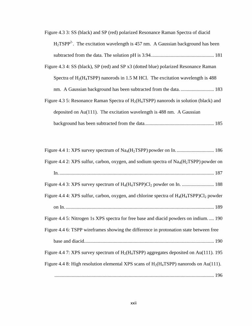
Figure 4.3 3: SS (black) and SP (red) polarized Resonance Raman Spectra of diacid
H2TSPP2-
. The excitation wavelength is 457 nm. A Gaussian background has been
subtracted from the data. The solution pH is 3.94. .................................................. 181
Figure 4.3 4: SS (black), SP (red) and SP x3 (dotted blue) polarized Resonance Raman
Spectra of H2(H4TSPP) nanorods in 1.5 M HCl. The excitation wavelength is 488
nm. A Gaussian background has been subtracted from the data. ........................... 183
Figure 4.3 5: Resonance Raman Spectra of H2(H4TSPP) nanorods in solution (black) and
deposited on Au(111). The excitation wavelength is 488 nm. A Gaussian
background has been subtracted from the data. ....................................................... 185
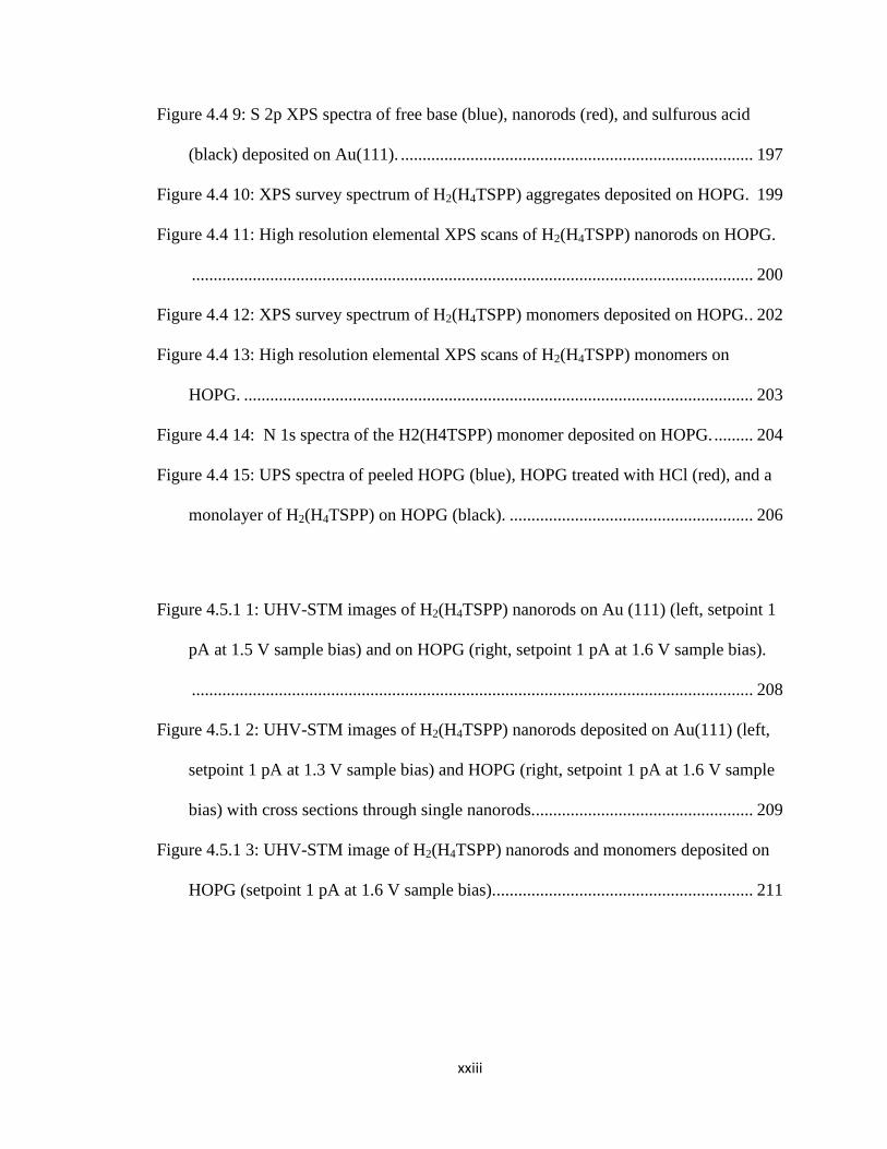
Figure 4.4 1: XPS survey spectrum of Na4(H2TSPP) powder on In. .............................. 186
Figure 4.4 2: XPS sulfur, carbon, oxygen, and sodium spectra of Na4(H2TSPP) powder on
In. ............................................................................................................................. 187
Figure 4.4 3: XPS survey spectrum of H4(H4TSPP)Cl2 powder on In. .......................... 188
Figure 4.4 4: XPS sulfur, carbon, oxygen, and chlorine spectra of H4(H4TSPP)Cl2 powder
on In. ........................................................................................................................ 189
Figure 4.4 5: Nitrogen 1s XPS spectra for free base and diacid powders on indium. .... 190
Figure 4.4 6: TSPP wireframes showing the difference in protonation state between free
base and diacid. ........................................................................................................ 190
Figure 4.4 7: XPS survey spectrum of H2(H4TSPP) aggregates deposited on Au(111). 195
Figure 4.4 8: High resolution elemental XPS scans of H2(H4TSPP) nanorods on Au(111).
................................................................................................................................. 196
xxiii
Figure 4.4 9: S 2p XPS spectra of free base (blue), nanorods (red), and sulfurous acid
(black) deposited on Au(111). ................................................................................. 197
Figure 4.4 10: XPS survey spectrum of H2(H4TSPP) aggregates deposited on HOPG. 199
Figure 4.4 11: High resolution elemental XPS scans of H2(H4TSPP) nanorods on HOPG.
................................................................................................................................. 200
Figure 4.4 12: XPS survey spectrum of H2(H4TSPP) monomers deposited on HOPG. . 202
Figure 4.4 13: High resolution elemental XPS scans of H2(H4TSPP) monomers on
HOPG. ..................................................................................................................... 203
Figure 4.4 14: N 1s spectra of the H2(H4TSPP) monomer deposited on HOPG. ......... 204
Figure 4.4 15: UPS spectra of peeled HOPG (blue), HOPG treated with HCl (red), and a
monolayer of H2(H4TSPP) on HOPG (black). ........................................................ 206
Figure 4.5.1 1: UHV-STM images of H2(H4TSPP) nanorods on Au (111) (left, setpoint 1
pA at 1.5 V sample bias) and on HOPG (right, setpoint 1 pA at 1.6 V sample bias).
................................................................................................................................. 208
Figure 4.5.1 2: UHV-STM images of H2(H4TSPP) nanorods deposited on Au(111) (left,
setpoint 1 pA at 1.3 V sample bias) and HOPG (right, setpoint 1 pA at 1.6 V sample
bias) with cross sections through single nanorods................................................... 209
Figure 4.5.1 3: UHV-STM image of H2(H4TSPP) nanorods and monomers deposited on
HOPG (setpoint 1 pA at 1.6 V sample bias)............................................................ 211
xxiv
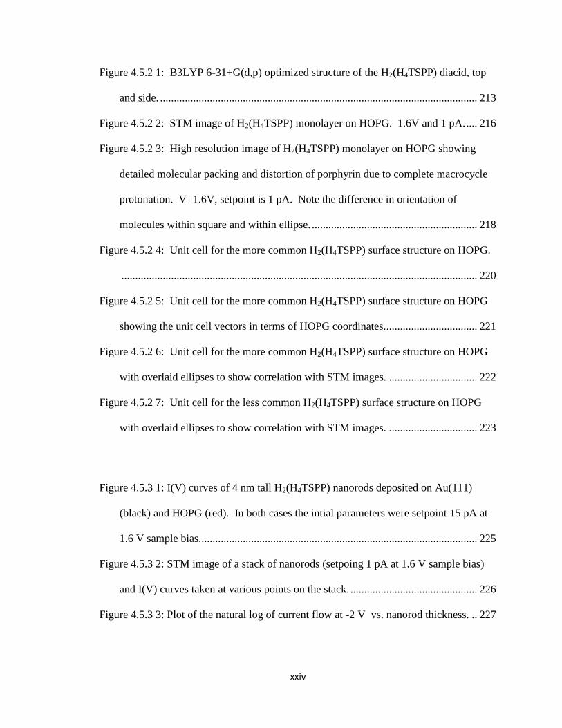
Figure 4.5.2 1: B3LYP 6-31+G(d,p) optimized structure of the H2(H4TSPP) diacid, top
and side. ................................................................................................................... 213
Figure 4.5.2 2: STM image of H2(H4TSPP) monolayer on HOPG. 1.6V and 1 pA. .... 216
Figure 4.5.2 3: High resolution image of H2(H4TSPP) monolayer on HOPG showing
detailed molecular packing and distortion of porphyrin due to complete macrocycle
protonation. V=1.6V, setpoint is 1 pA. Note the difference in orientation of
molecules within square and within ellipse. ............................................................ 218
Figure 4.5.2 4: Unit cell for the more common H2(H4TSPP) surface structure on HOPG.
................................................................................................................................. 220
Figure 4.5.2 5: Unit cell for the more common H2(H4TSPP) surface structure on HOPG
showing the unit cell vectors in terms of HOPG coordinates.................................. 221
Figure 4.5.2 6: Unit cell for the more common H2(H4TSPP) surface structure on HOPG
with overlaid ellipses to show correlation with STM images. ................................ 222
Figure 4.5.2 7: Unit cell for the less common H2(H4TSPP) surface structure on HOPG
with overlaid ellipses to show correlation with STM images. ................................ 223
Figure 4.5.3 1: I(V) curves of 4 nm tall H2(H4TSPP) nanorods deposited on Au(111)
(black) and HOPG (red). In both cases the intial parameters were setpoint 15 pA at
1.6 V sample bias..................................................................................................... 225
Figure 4.5.3 2: STM image of a stack of nanorods (setpoing 1 pA at 1.6 V sample bias)
and I(V) curves taken at various points on the stack. .............................................. 226
Figure 4.5.3 3: Plot of the natural log of current flow at -2 V vs. nanorod thickness. .. 227
xxv
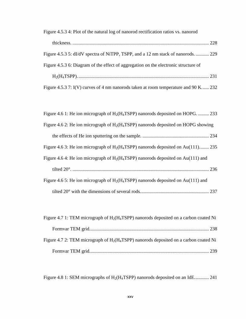
Figure 4.5.3 4: Plot of the natural log of nanorod rectification ratios vs. nanorod
thickness. ................................................................................................................. 228
Figure 4.5.3 5: dI/dV spectra of NiTPP, TSPP, and a 12 nm stack of nanorods. ........... 229
Figure 4.5.3 6: Diagram of the effect of aggregation on the electronic structure of
H2(H4TSPP). ............................................................................................................ 231
Figure 4.5.3 7: I(V) curves of 4 nm nanorods taken at room temperature and 90 K. ..... 232
Figure 4.6 1: He ion micrograph of H2(H4TSPP) nanorods deposited on HOPG. ......... 233
Figure 4.6 2: He ion micrograph of H2(H4TSPP) nanorods deposited on HOPG showing
the effects of He ion sputtering on the sample. ....................................................... 234
Figure 4.6 3: He ion micrograph of H2(H4TSPP) nanorods deposited on Au(111). ....... 235
Figure 4.6 4: He ion micrograph of H2(H4TSPP) nanorods deposited on Au(111) and
tilted 20°. ................................................................................................................. 236
Figure 4.6 5: He ion micrograph of H2(H4TSPP) nanorods deposited on Au(111) and
tilted 20° with the dimensions of several rods. ........................................................ 237
Figure 4.7 1: TEM micrograph of H2(H4TSPP) nanorods deposited on a carbon coated Ni
Formvar TEM grid................................................................................................... 238
Figure 4.7 2: TEM micrograph of H2(H4TSPP) nanorods deposited on a carbon coated Ni
Formvar TEM grid................................................................................................... 239
Figure 4.8 1: SEM micrographs of H2(H4TSPP) nanorods deposited on an IdE. ........... 241
xxvi
Figure 4.8 2: I(V) curve of H2(H4TSPP) nanorods deposited on an IdE and an IdE treated
with HCl. Both measurements were taken with the samples in a closed box to
prevent photoconductivity. ...................................................................................... 242
List of Tables
Table 1.1 1: Absorbance bands for two different Zn porphyrins. ...................................... 4
Table 1.1 2: Electrochemical and absorbance data for metalated octaethyl porphyrins.
The potentials are vs. SCE and taken in methanol or chloroform-methanol. data
from reference ............................................................................................................. 5
Table 1.2.3 1: Reported dimensions of H2(H4TSPP) nanorods prepared under different
conditions. (* Apparent height) ................................................................................ 25
Table 4.3 1: Vibrational mode positions (Δυ in cm-1
) and assignments of TSPP........... 177
Table 4.4 1: Theoretical and experimental elemental ratios in TSPP free base and diacid
powders. ................................................................................................................... 191
Table 4.4 2: Elemental ratios of Na4(H2TSPP) by XPS, Columbia Analytical Services,
and the theoretical values. ....................................................................................... 192
Table 4.4 3: Elemental ratios of H4(H4TSPP)Cl2 by XPS, Columbia Analytical Services,
and the theoretical values. ....................................................................................... 193
xxvii
Table 4.4 4: Elemental ratios of H4(H4TSPP)Cl2 by XPS, Columbia Analytical Services,
and the theoretical values. ....................................................................................... 194
Table 4.4 5: Atomic ratios by XPS of the theoretical diacid, diacid powder, and nanorods
deposited on Au(111). ............................................................................................. 198
Table 4.4 6: Atomic ratios by XPS of the theoretical diacid, diacid powder, and nanorods
deposited on HOPG. ................................................................................................ 202
Table 4.4 7: Atomic ratios by XPS of the theoretical diacid, diacid powder, and nanorods
deposited on HOPG. ................................................................................................ 205
Table 4.4 8: Peak positions in eV of the elements studied by XPS. ............................... 205
Table 4.5.2 1: Electron Affinity values in Different Phases a) Reference 194; b)
E1/2+4.71 V; c) Reference 191; d) The work function for NiTPP/Au(111) taken as
5.2 eV and that for ................................................................................................... 215
Table 4.5.2 2: Ionization Potential values in Different Phases a) Reference 194; b)
E1/2+4.71 V; c) Reference 191; d) The work function for NiTPP/Au(111) taken as
5.2 eV and that for H2(H4TSPP)/HOPG as 4.9 eV; e) Reference 195; f) Reference
196; g) Reference 192; h) UPS data from reference assuming the Ag work function
was 4.6 eV. .............................................................................................................. 215
xxviii
Glossary of Terms
AFM: Atomic Force Microscopy
BO Approximation: Born Oppenheimer Approximation
DFT: Density Functional Theory
DLS: Dynamic Light Scattering
EA: Electron Affinity
EB: Binding Energy
EDS: Electron Dispersive Spectroscopy
EF: Fermi Energy
Ekin: Kinetic Energy
ELS: elastic light scattering
EV: Vacuum Energy
HIM: Helium Ion Microscope
HOPG: Highly Ordered Pyrolytic Graphite
IdE: Interdigitated Electrode
IP: Ionization Potential
IR: Infrared Spectroscopy
xxix
KHD: Kramers-Heisenberg-Dirac
LDOS: local density of states
Nanorod/Nanotube: Idiomatic for H2(H4TSPP) aggregate
NiTPP: Nickel Tetraphenylporphyrin
OMTS: orbital mediated tunnleing spectroscopy
Q-Band: An absorbance band to the red of the Soret band in a porphyrin
RLS: Resonance Light Scattering
SAXS: Small Angle X-ray Scattering
SCE: saturated calomel electrode
SEM: Scanning Electron Microscope
Soret (B) -band: A strong absorbance in the blue region of the UV-visible spectrum of a
porphyrin
SPM: Scanning Probe Microscopy
STM: Scanning Tunneling Microscopy
TEM: Transmission Electron Microscope
UHV: Ultrahigh Vacuum
UPS: Ultraviolet Photoelectron Spectroscopy

xxx
UV-visible: Ultraviolet-Visible Spectroscopy
WKB: Wentzel-Kramers-Brillouin
XPS: X-ray Photoelectron Spectroscopy
1
Chapter 1: Introduction
1.1 Properties and Applications of Porphyrins
Porphyrins are a class of aromatic organic compounds composed of carbon,
nitrogen, and hydrogen. Porphyrins were first described by Alfred Treibs in 1936 as a
part of his work in the field of geochemistry.1 The most basic porphyrin, called porphine,
is a 24-membered ring composed of four pyrroles connected by methine bridges. This
24-membered ring is referred to as the macrocycle. The electronic structure of
porphyrins is of central importance to this work and will be covered in detail in a separate
section. Porphyrin compounds are highly varied so it is worthwhile to briefly cover
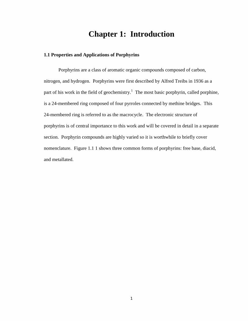
nomenclature. Figure 1.1 1 shows three common forms of porphyrins: free base, diacid,
and metallated.
2
Figure 1.1 1: Three forms of porphine, free base, diacid, and metallated along with the
nomeclature tracking the poisitions of substituent groups.
The terminology with respect to protonation of the nitrogens is straightforward.
The free base has two unprotonated nitrogens which can accept hydrogen ions, hence the
term base. In this form the molecule has a neutral charge and is assigned D2h symmetry.
The diacid‟s nitrogens are fully protonated and the overall molecular charge is +2.
Protonation of the macrocycle nitrogens has important effects on the molecule‟s
geometry. To first approximation the diacid belongs to the D4h point group and is
commonly treated as such. In reality the macrocycle is not large enough to accommodate
four hydrogens so the molecule adopts a saddled geometry.2 The saddled nature of
porphyrin diacids is an important factor to consider during the study of porphyrin
aggregation and its organization on substrates. Metallated porphyrins are synthesized by
3
replacing the two central hydrogens with a metal ion such as (but not limited to) Co, Ni,
Cu, Zn, and Mg.3 R groups can be added to the base porphine unit in order to affect the
molecule‟s properties. For example, substituting benzoic acid groups at the meso
positions on the ring would increase solubility in water and add intermolecular hydrogen
bonding interactions. Pyridyl substitution at the meso position adds additional proton
acceptor sites creating the potential of a highly charged ion in acidic solutions. The
macrocycle carbons are named as shown in Figure 1.1 1, and the position of substituent
groups is tracked by the appropriate number or Greek letter.4 For example, if phenyl
groups were attached at the α and β positions the molecule would be α,β-
diphenylporphine.
Porphyrins are an important family of compounds for several reasons. They can
serve as components in solar cells5, non-linear optical devices
6, sensors
7, act as catalysts
8,
and serve as sensitizers in photodynamic tumor therapy9. One of the major strengths of
porphyrins is flexibility. Porphine can be modified in a number of ways by adding R
groups and substituting metals into the macrocycle. Modifications to the base porphine
unit affect its optical and electronic properties allowing porphyrins to be tuned to a
particular use. Consider the absorption spectra of Zn(II)-1,2,3,4,5,6,7,8-
octaethylporphine and Zn(II)-α,β,γ,δ-tetraphenylporphine, the two species differ only in
the substituents attached to the macrocycle.
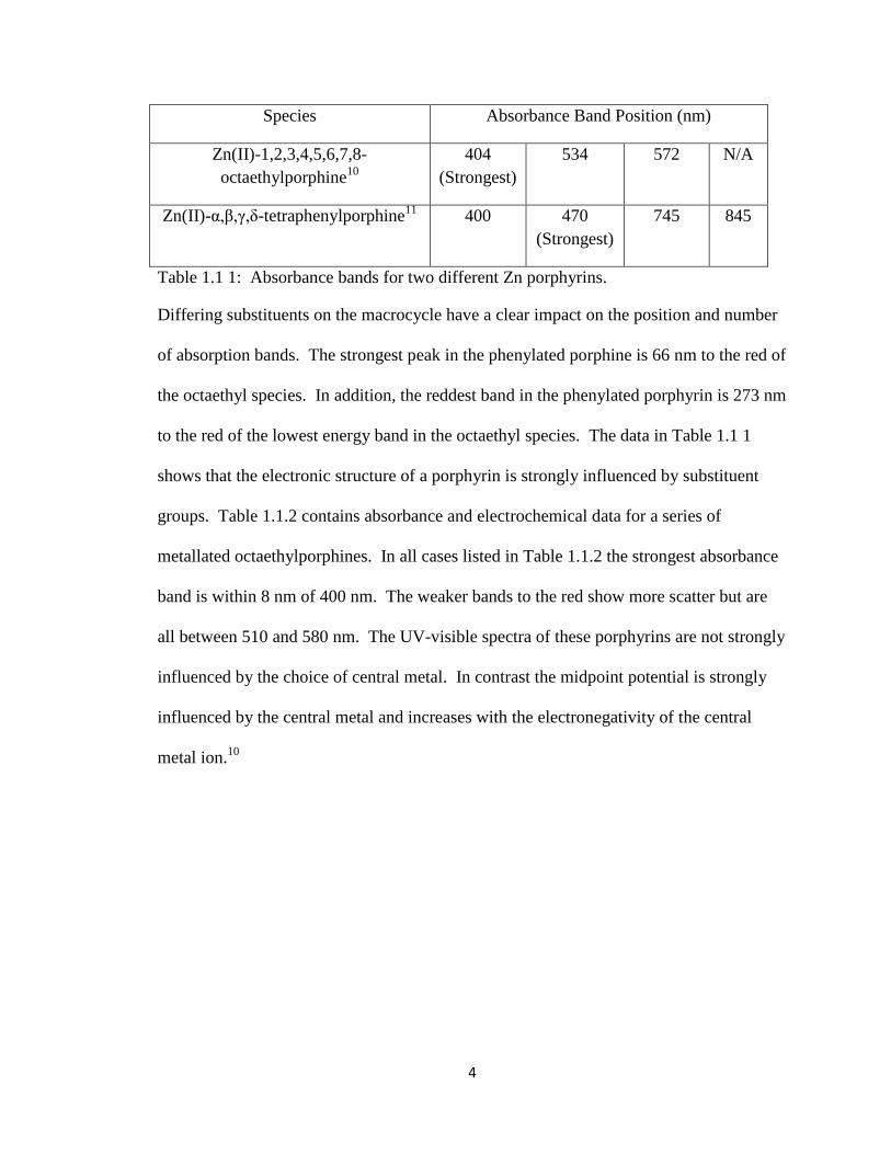
4
Species Absorbance Band Position (nm)
Zn(II)-1,2,3,4,5,6,7,8-
octaethylporphine10
404
(Strongest)
534 572 N/A
Zn(II)-α,β,γ,δ-tetraphenylporphine11
400 470
(Strongest)
745 845
Table 1.1 1: Absorbance bands for two different Zn porphyrins.
Differing substituents on the macrocycle have a clear impact on the position and number
of absorption bands. The strongest peak in the phenylated porphine is 66 nm to the red of
the octaethyl species. In addition, the reddest band in the phenylated porphyrin is 273 nm
to the red of the lowest energy band in the octaethyl species. The data in Table 1.1 1
shows that the electronic structure of a porphyrin is strongly influenced by substituent
groups. Table 1.1.2 contains absorbance and electrochemical data for a series of
metallated octaethylporphines. In all cases listed in Table 1.1.2 the strongest absorbance
band is within 8 nm of 400 nm. The weaker bands to the red show more scatter but are
all between 510 and 580 nm. The UV-visible spectra of these porphyrins are not strongly
influenced by the choice of central metal. In contrast the midpoint potential is strongly
influenced by the central metal and increases with the electronegativity of the central
metal ion.10
5
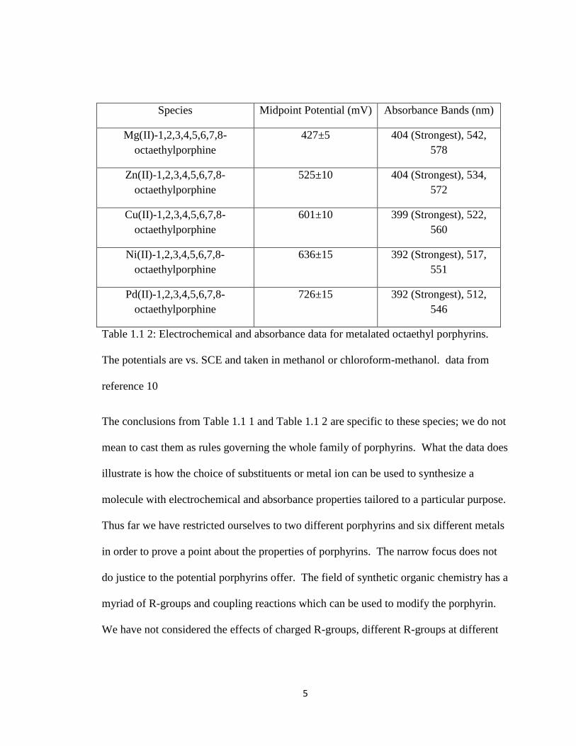
Species Midpoint Potential (mV) Absorbance Bands (nm)
Mg(II)-1,2,3,4,5,6,7,8-
octaethylporphine
427±5 404 (Strongest), 542,
578
Zn(II)-1,2,3,4,5,6,7,8-
octaethylporphine
525±10 404 (Strongest), 534,
572
Cu(II)-1,2,3,4,5,6,7,8-
octaethylporphine
601±10 399 (Strongest), 522,
560
Ni(II)-1,2,3,4,5,6,7,8-
octaethylporphine
636±15 392 (Strongest), 517,
551
Pd(II)-1,2,3,4,5,6,7,8-
octaethylporphine
726±15 392 (Strongest), 512,
546
Table 1.1 2: Electrochemical and absorbance data for metalated octaethyl porphyrins.
The potentials are vs. SCE and taken in methanol or chloroform-methanol. data from
reference 10
The conclusions from Table 1.1 1 and Table 1.1 2 are specific to these species; we do not
mean to cast them as rules governing the whole family of porphyrins. What the data does
illustrate is how the choice of substituents or metal ion can be used to synthesize a
molecule with electrochemical and absorbance properties tailored to a particular purpose.
Thus far we have restricted ourselves to two different porphyrins and six different metals
in order to prove a point about the properties of porphyrins. The narrow focus does not
do justice to the potential porphyrins offer. The field of synthetic organic chemistry has a
myriad of R-groups and coupling reactions which can be used to modify the porphyrin.
We have not considered the effects of charged R-groups, different R-groups at different
6
positions, reducing one of the double bonds in the macrocycle, or any number of other
modifications. The possibilities of these molecules are as broad as our imaginations.
The vast potential of porphyrin chemistry becomes almost limitless when we
consider self-assembled supramolecular aggregates of porphyrins. A molecular
aggregate is an ordered array of molecular units12
and it has been shown that dimers and
larger aggregates can exhibit properties which are different from the parent molecules.13
Molecular self-assembly is the spontaneous association of molecules under equilibrium
conditions into stable, structurally well-defined aggregates joined by noncovalent
bonds.14
Just as the characteristics of a porphyrin monomer can be influenced by things
like substituent groups the characteristics of molecular aggregates are strongly influenced
by their constituent molecules. Supramolecular structures could be made from a single
type of porphyrin, porphyrins with different or opposing charges, metallated with non-
metalated, two porphyrins with different metals, water-soluble with water-insoluble, a
porphyrin with another type of molecule, and so forth. The experimental conditions may
also play a role in the properties of supramolecular aggregates. A particular aggregate
may form in solution, or at a solution-surface interface, or upon vapor deposition of the
constituents. The extensive library of porphyrin compounds offers a wellspring of
species to be used in the synthesis of molecular aggregates; with the choice of building
block influencing the properties of entire aggregate.
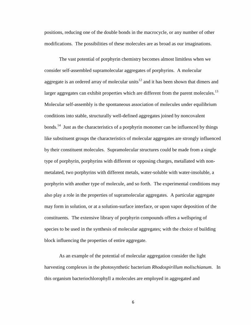
As an example of the potential of molecular aggregation consider the light
harvesting complexes in the photosynthetic bacterium Rhodospirillum molischianum. In
this organism bacteriochlorophyll a molecules are employed in aggregated and
7
unaggregated forms to widen the range over which the light needed for photosynthesis
can be absorbed and to improve photosynthetic efficiency.15
The light harvesting
complexes are composed of a ring of bacteriochlorophyll a molecules (the aggregate) and
isolated monomers.
Figure 1.1 2: Crystal structure of a light harvesting complex in Rhodospirillum
molischianum. Green squares are aggregated bacteriochlorophyll a molecules, blue
squares are monomeric bacteriochlorophyll a, and the yellow structures are carotenoids.
image from reference 15
Monomeric bacteriochlorophyll a has an electronic absorption band at 800 nm, while the
ring porphyrins absorb at 850 nm. By employing both the ring-shaped aggregate and the
monomer a bacterium can absorb photons over a wider range of the electromagnetic
spectrum. In addition to widening the absorption envelope the complexes are capable of
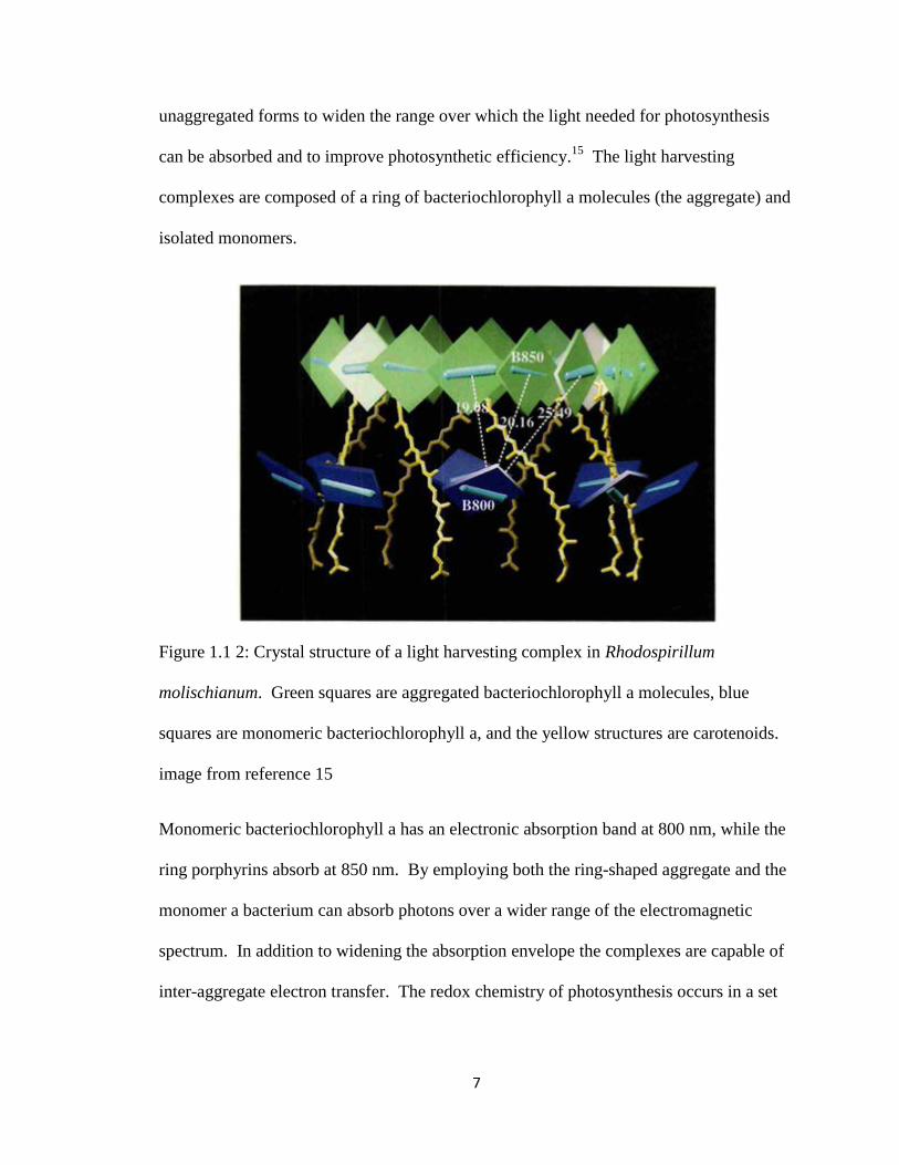
inter-aggregate electron transfer. The redox chemistry of photosynthesis occurs in a set
8
of bacteriochlorophyll a molecules called the special pair. The special pair can run
photosynthetic redox reactions 100 times faster than it can absorb light.15
In order to
increase the efficiency of the process the special pair is surrounded by a circular
aggregate of 16 bacteriochlorophyll a molecules called light harvesting complex I. Light
harvesting complex I is in turn surrounded by many circular aggregates called light
harvesting complex II (see Figure 1.1 3). Photons are absorbed by light harvesting
complex II and transferred from complex to complex until they reach the special pair.
This arrangement of complexes increases photon absorption, providing electrons to the
special pair at an accelerated rate increasing photosynthetic efficiency.15
Figure 1.1 3: Schematic of photon absorption and electron transport among light
harvesting complexs in Rhodospirillum molischianum. image from reference 15
The light harvesting complexes in Rhodospirillum molischianum provide a powerful
example of the importance and capabilities of molecular aggregates. A second example
of the importance of molecular aggregation is nanowires formed by metallated
1,2,3,4,5,6,7,8-octaethylporphine (Co, Ni, Cu, Zn, and Mg).3 Aggregates 200 nm wide
and several microns long can be formed by vapor depositing metalated
9
octaethylporphyrin on varying substrates. The nanowires were used to bridge electrical
contacts and were shown to be both photoconducting and field-emissive. Molecular
aggregates are also potentially useful in the field of catalysis. Co(II)-α,β,γ,δ-
tetrasulfonatophenylporphine electropolymerized with aniline forms nanowires 30-50 nm
across and 500 nm long.16
When deposited on a glassy carbon electrode the aggregates
proved capable of reducing molecular oxygen illustrating the possible utility of molecular
aggregates as components in fuel cells.16
These examples demonstrate that molecular aggregates have great potential as
device components. In order to effectively utilize molecular aggregates in practical
applications a more fundamental understanding of their formation, structure, electronic
properties, and the interplay of these three features is needed. A firm grasp of the integral
concepts of molecular aggregation will open up the possibility of constructing nanoscale
wires, switches, diodes, capacitors, and other electronic components simply by selecting
a suitable constituent molecule.
1.2 Literature Review of Porphyrin Aggregation
In the last decade there has been tremendous interest in inorganic,17-21
metallic,22-
26 and carbon
27-30 nanostructures. Applications of these nanostructures range over a wide
area, including hydrogen storage,31,32
studies of living cells,33
drug delivery,34
photonic
materials,18
sensing and detecting,35-37
optics,38
catalysis,22,39
and electronic devices.40
Organic nanostructures are also known,41-46
and are especially intriguing because of the
wide range of compounds from which they may be made. This advantage is greatly
magnified by the demonstrated fact that the optical and electronic properties of organic
10
nanostructures clearly differ from those of the bulk materials.16,47-49
For example
supramolecular nanorods of 5,15-diaryl substituted porphyrins exhibit a much broader
absorption spectrum than simply deposited material.48
An interesting class of these organic nanostructures is the self-assembled
structures built from porphyrins.3,49-53
The ease of synthesis and robust character of
porphyrin based materials allows for the production of a novel class of nanomaterials
with potential applications in catalysis, sensor, solar cells, and electronic devices.50
The
shapes formed upon aggregation are highly varied ranging from spheres to flower-like
structures to rods. Porphyrin aggregates range in shape and size as the porphyrin
skeleton can be substituted in a number of different ways resulting in different
intermolecular interactions.
1.2.1 Non-Ionic Porphyrin Aggregates in Solution and at Surfaces
Porphyrin aggregates formed in solutions take several forms. PdCl2 linked
porphyrin dimers in a toluene solution act as molecular tweezers in a complexation
reaction with fullerenes.54
Fullerenes complexed in the “jaws porphyrin” have
fluorescence and absorbance spectra which are not a sum of the two constituent
compounds indicating that complexation induces changes in electronic structure. The
complex also has potential applications in photoconduction. A second example of
porphyrin containing chelating agents is a pair of zinc porphyrins connected by an
aromatic oligoamid spacer.55
This porphyrin has been shown to chelate crown ethers.
11
Examples of non-ionic porphyrin aggregates forming larger aggregates are also
known. Both α-(3‟-pyridyl)-β,γ,δ-tris(4‟-carboxyphenyl)porphine and α-(2‟-quinolyl)-
β,γ,δ-tris(4‟-hydroxyphenyl)porphine form extensive sheet-like aggregates upon
evaporation of the chloroform/ethanol solvent.56
The aggregate is held together by
hydrogen bonding between carboxyl and pyridyl groups in the case of α-(3‟-pyridyl)-
β,γ,δ-tris(4‟-carboxyphenyl)porphine and hydroxyl and quinone groups in α-(2‟-
quinolyl)-β,γ,δ-tris(4‟-hydroxyphenyl)porphine aggregates. While both porphyrins form
extensive hydrogen bonded networks the structures are different indicating that the
choice of R-group can influence aggregate morphology. Rings ranging from 10 nm to 10
µm in diameter and up to 200 nm tall can be formed on both glass and graphite substrates
by the evaporation of bis(21H,23H-α(4-pyrydyl)-β,γ,δ-tris(4-
hexadecyloxyphenyl)porphine)platinum dichloride dissolved in chloroform.57
Comparison of UV-visible spectra of the porphyrin dissolved in chloroform and on glass
shows shifts in visible absorption bands upon solvent evaporation indicating electronic
coupling among constituent molecules. In both cases it appears that the increase in
concentration by solvent evaporation is an important driver in aggregation.
1.2.2 Ionic Porphyrin Aggregates in Solution and on Surfaces
Of particular interest to us, are the porphyrin nanostructures created by ionic self-
assembly. Ionic self-assembly is the coupling of structurally different simple ionic
blocks (charged tectons), or structurally similar (or identical) zwitterionic building
blocks. Instead of hydrogen bonding or Van der Waals interactions the aggregate is held
together by stronger electrostatic interactions. It is logical to divide our discussion of
12
ionic porphyrin aggregation in to two sections: solution and solid phase studies. Solution
phase studies are important because the systems discussed in this section aggregate in
solution. Spectroscopic techniques such as UV-visible spectroscopy and Resonance
Light Scattering (RLS) are useful for studying aggregation processes in solution. While
important, optical spectroscopy is not well suited for studying the shapes of aggregates.
Microscopic techniques such as scanning electron microscopy (SEM), transmission
electron microscopy (TEM), and scanning probe microscopy (SPM) can provide detailed
structural data that optical spectroscopy can not. With the notable exception of SEM
images of frozen solutions these three microscopy techniques are not capable of
visualizing an aggregate in solution. SEM and TEM require samples to be under vacuum
during analysis. The deposition and desiccation of aggregates necessary for SEM and
TEM may influence the structure and/or properties of the system. Solution phase SPM
offers the opportunity to study aggregates in solution, but the aggregates still must be
deposited on a substrate. It is important to remember that the deposition and desiccation
typically required for microscopy of aggregates formed in solution may cause changes in
the aggregate structure and or properties.
α,β,γ,δ-tetraphosphonatophenylporphine (H2TPPP) forms aggregates in aqueous
solutions at low pH‟s, and in the presence of a G5 poly(amidoamine) dendrimer.58
The
charge on H2TPPP is pH dependant, in basic solution each phosphonato group is -2 for a
total charge of -8. Below pH 2 the phosphonato groups are protonated and uncharged
while the macrocycle is +2 due to nitrogen protonation. Both dendrimer and acid
addition cause changes to the H2TPPP absorption spectrum indicative of solution phase
13
aggregation. Weak RLS indicates that the solution phase aggregate are relatively small.
When H2TPPP in solution with G5 poly(amidoamine) is deposited on HOPG aggregates
ranging from globules tens of nanometers wide to strings up to 300 nm are observed by
AFM.58
A similar molecule, α,β,γ,δ-tetracarboxyphenylporphine (H2TCPP) forms
aggregates in acidic solutions as well.59
Tetracarboxyphenyl porphyrin is similar to
α,β,γ,δ-tetraphosphonatophenylporphine; the only structural difference is the carboxylate
vs. phosphonate groups. Similarly to the H2TPPP case the peripheral acid groups and
macrocycle nitrogens of H2TCPP protonate in acidic solutions resulting in an ion with a
+2 charge. H2TCPP is an interesting case because its aggregation is sensitive to the type
of acid used. Monomeric H2TCPP‟s Soret band is located at 440 nm, upon addition of
sufficient HCl to reach pH 0.9 the 440 nm absorbance dies away and a new band grows
in at 417 nm. If nitric acid is used to reach the same pH the monomer band decreases in
favor of two new bands at 406 and 467 nm. The appearance of different absorption
bands upon addition of different acids suggests that aggregate formation is a function of
acid species. RLS data of H2TCPP aggregated in both HCl and HNO3 is consistent with
the formation of different aggregates with different acids. The RLS spectrum of H2TCPP
in HCl shows little scattering which indicates small aggregates. H2TCPP aggregated in
HNO3 has a sharp RLS peak superimposed on a broad scattering background which
indicates that the aggregates formed in nitric acid are larger than those formed in HCl.
Deposition of both solutions on silica provides further evidence of aggregation as a
function of acid.60
AFM images of the HCl aggregate reveal rings with diameters of 200-
2000 nm and heights of 4-5 nm. Aggregates formed in nitric acid were rod-shaped ~4
nm tall ~20 nm wide and microns long. H2TCPP is an interesting aggregation case study
14
due to its dependence on the acid species used to induce aggregation. Ionic porphyrin
aggregates are not limited to rod and ring structures. Four-leaf clover-shaped aggregates
5 µm in diameter can be made from a mixture of ZnIIT(N-EtOH-4-Py)P
4+ and
SnIV
tetrasulfonatophenylporphine.50
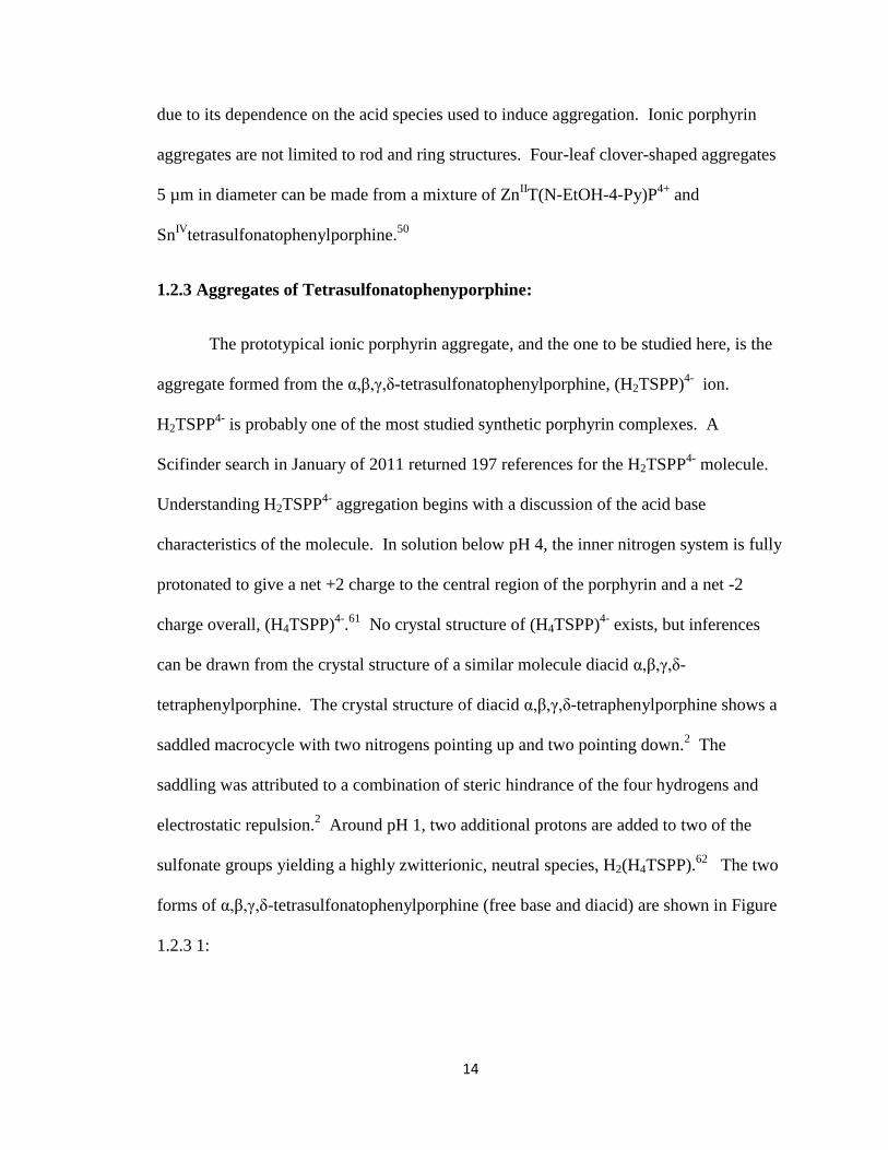
1.2.3 Aggregates of Tetrasulfonatophenyporphine:
The prototypical ionic porphyrin aggregate, and the one to be studied here, is the
aggregate formed from the α,β,γ,δ-tetrasulfonatophenylporphine, (H2TSPP)4-
ion.
H2TSPP4-
is probably one of the most studied synthetic porphyrin complexes. A
Scifinder search in January of 2011 returned 197 references for the H2TSPP4-
molecule.
Understanding H2TSPP4-
aggregation begins with a discussion of the acid base
characteristics of the molecule. In solution below pH 4, the inner nitrogen system is fully
protonated to give a net +2 charge to the central region of the porphyrin and a net -2
charge overall, (H4TSPP)4-
.61
No crystal structure of (H4TSPP)4-
exists, but inferences
can be drawn from the crystal structure of a similar molecule diacid α,β,γ,δ-
tetraphenylporphine. The crystal structure of diacid α,β,γ,δ-tetraphenylporphine shows a
saddled macrocycle with two nitrogens pointing up and two pointing down.2 The
saddling was attributed to a combination of steric hindrance of the four hydrogens and
electrostatic repulsion.2 Around pH 1, two additional protons are added to two of the
sulfonate groups yielding a highly zwitterionic, neutral species, H2(H4TSPP).62
The two
forms of α,β,γ,δ-tetrasulfonatophenylporphine (free base and diacid) are shown in Figure
1.2.3 1:
15
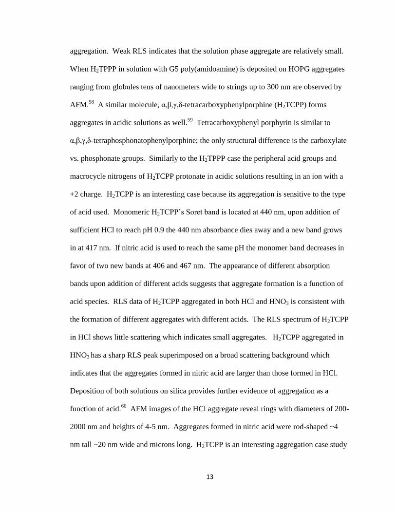
Figure 1.2.3 1: Two forms of tetrasulfonatophenyporphine: free base and diacid.
It is thought that the combination of electrostatic attraction between peripheral negative
sulfonate groups and +2 central regions, and the π-π interactions of adjacent porphyrins
hold the aggregate together. The co-planar or staircase model is often used to describe
the aggregation of H2(H4TSPP).58,63-69
In the staircase model a negative sulfonato group
interacts with the positive macrocycle forming a dimer as pictured in Figure 1.2.3 2.
More molecules can be added to the dimer to create aggregates which are very long. The
models in Figure 1.2.3 2 were individually optimized in the gas phase and do not take in
to account any geometry changes that may occur upon aggregation.
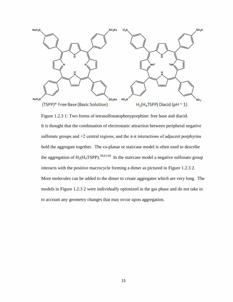
16
Figure 1.2.3 2: Structure of an H2(H4TSPP) dimer.
With an understanding of the H2(H4TSPP) dimer structure we now turn to a
discussion of aggregate formation. Under acidic, aqueous conditions (usually pH <2), the
diacid species of the porphyrin, H2(H4TSPP), forms aggregates.51,64,65,70-79
Formation of
these aggregates can also be induced by other cationic species including alkali metal
ions,51,72,80,84
surfactants,85,86
ionic liquids,87
and cationic porphyrins.88
The aggregation
of H2(H4TSPP) is signaled by changes in UV-visible spectra.63,66,72,81, 89-92
Upon
aggregation of H2(H4TSPP) the monomeric absorbance bands at 434, 595, and 644 nm
decrease in favor of new transitions at 424, 490, and 707 nm. The 490 nm band of the
aggregate has been assigned to a Frenkel exciton transition, and its sharpness has been
interpreted in terms of motional narrowing, which averages the local inhomogeneities.93
In the absence of disorder, the line width is inversely proportional to N1/2
, where N is the
number of coherently coupled chromophores (or coherence number), which has been
estimated to be in the range 11-120 for the H2(H4TSPP) aggregate.94
Aggregation of
H2(H4TSPP) also results in perturbations to the bands at about 600-700 nm, which are red
shifted and enhanced in intensity relative to the monomer.93,95-97
17
Kinetic studies of H2(H4TSPP) aggregate formation have been previously
reported. One of the experiments involved mixing a porphyrin solution with acid
followed by monitoring the absorbance at 490 nm.89
An initial induction period followed
by a rapid increase in the aggregate absorbance at 490 nm was observed. The induction
period was attributed to a rate-limiting nucleation step followed by aggregate growth. A
similar study was carried out using NaCl to start the aggregation process.81
This study
also reported an induction period followed by a rapid increase in the 490 nm aggregate
absorbance. Concurrent with the 490 nm data trends in absorbance at 434 and 413 nm
were also monitored. The monomer band at 434 nm began decreasing slowly during the
induction period followed by a more rapid drop afterward consistent with a mechanism
where nucleation is rate-limiting. The absorbance at 413 nm increased marginally during
the induction period and began decreasing at the same time as the monomer band. The
413 nm absorbance was attributed to the formation of an intermediate species. The
authors did not speculate on the identity of the intermediate.
UV-visible spectroscopy is capable of probing the kinetics of aggregation and
changes in electronic structure, but not the number of molecules or size of an aggregate in
solution. To answer these questions we turn to RLS, Dynamic Light Scattering (DLS),
and Small Angle X-ray Scattering (SAXS). RLS is a useful spectroscopic technique for
studying aggregates because it is sensitive to particle size. Light scattering increases with
the square of the volume of the scatterer98
so large aggregates have strong RLS signals.
The size selectivity is very helpful when studying UV-visible spectra of solutions with
monomer/aggregate equilibrium as only the aggregate peaks will scatter.99
RLS studies
18
of H2(H4TSPP) aggregates consistently show a strong scattering signal at 490 nm
indicating the presence of a large aggregate in solution.58,99-101
This technique has been
employed to estimate the aggregation number of H2(H4TSPP) as being quite large, on the
order of 105.100
DLS studies of aggregates estimate the size of the H2(H4TSPP)
aggregates as ranging from 0.6 to 1.5 µm wide.69,70
SAXS data is consistent with the
large aggregate sizes indicated by RLS and DLS. SAXS scattering profiles are fit by a
hollow cylinder of radius 7.0 nm, wall thickness of 2.1 nm, and length 350 nm.71
A
region of “an impressive higher electron density value relative to the solvent” was
assigned as the shell of the aggregate tube. The scattering signal from the interior of the
tube was similar to, but not equal to the solvent. The authors did not speculate as to the
makeup of the tube‟s interior.
Raman studies of both monomeric and aggregated H2(H4TSPP) have been carried
out at different excitations. Excitation wavelengths of 488 nm64,72,80,102
and 413 nm102
have been employed to study aggregated H2(H4TSPP). The 488 and 413 nm laser lines
were used because they fall within the excitation envelopes of the 490 and 424 nm
aggregate transitions. Raman spectra at non-resonant wavelengths of 457.9 nm72,102
and
514.0 nm80
have also been reported. The Raman spectrum of aggregated H2(H4TSPP)
excited at 488 nm is dominated by two low frequency modes at 242 and 316 cm-
1.64,72,80,102
The 242 and 316 cm-1
bands have been assigned as out of plane saddling and
an in plane porphyrin breathing modes respectivly.102
These two modes are intimately
connected with the 490 nm transition of the aggregate. Raman spectra excited at
wavelengths other than 488 nm have much weaker low frequency modes.64,72,80,102
19
Enhanced intensity of low frequency modes has been reported for aggregates of H2TCPP
as well.59,64
Raman spectra of aggregated H2(H4TSPP) excited at 413 nm were not
subjected to extensive interpretation. The author only went as far as to say that the
species responsible for the 424 nm band is the same as the species responsible for the 490
nm band because the positions of the bands in the Raman spectra are very similar.102
Raman spectra of monomeric H2(H4TSPP) excited at 457.9 nm show vibrational modes
of similar energies to the aggregate. Some shifts of ~ 6-10 cm-1
in macrocycle modes are
observed which were attributed to increased planarity of the macrocycle upon
aggregation.102
The interpretation of H2(H4TSPP) Raman spectra were carried out in
terms of the staircase model of aggregation and tended to attribute changes in the position
of vibrational bands in terms of changes in the shape of the molecules upon aggregation.
Aggregates of H2(H4TSPP) exhibit interesting optical properties upon interaction
with polarized light. If a solution containing H2(H4TSPP) aggregates is passed through a
narrow (0.5 mm) tube the tubular aggregates will preferentially align themselves with
their long axes parallel to the flow direction.72
Absorption studies of plane-polarized
light oriented parallel and perpendicular to the direction of flow (and the long axis of the
aggregate) indicate that the aggregate visible absorption bands are polarized in different
directions. The bands at 490 nm and 707 nm are polarized down the long axis of the
aggregate while the band at 424 nm is polarized perpendicular to the aggregate long
axis.72
Circular dichroic spectra show a very curious interaction with polarized light.
Absorption studies of circularly polarized light can be used to determine the chirality of
species in solution. Circular dichroism studies show that aggregates of H2(H4TSPP) are
20
chiral and that different isomers form based upon the preparation of the aggregate
solution. If a solution of achiral H2(H4TSPP) is aggregated in the presence of chiral L-
lysine circular dichroism spectra show that chiral aggregates form.101
The same effect is
seen when L-tartaric acid is used.72
Interestingly, stirring the solution during aggregation
also produces chiral aggregates.72
Aggregates formed while the solution was stirred
clockwise are different isomers than aggregates formed during counterclockwise stirring.
No stirring yielded inconsistent spectra. These two factors; the polarization of the
absorbance bands and aggregate chirality are helpful in evaluating proposed aggregation
models.
A great deal of effort has been put forth over the past few years to obtain detailed
structural information about the supramolecular assemblies of H2(H4TSPP) molecules.
Studies employing fluorescence microscopy,103
electron microscopy,62
atomic force
microscopy (AFM),51,58,73,75,101,104-107
and scanning tunneling microscopy (STM)73
provide useful but varied information about the geometrical sizes of the aggregates but
could not resolve their structure at the molecular level. Since the molecular level
arrangement of monomers in an aggregate influence the electronic and optical properties
of the aggregate an understanding of the interplay between structure, electronic
properties, and optical properties is critical to the study of functional nanomaterials.
Complementary to the SAXS, RLS, and DLS studies is the cryo-electron
microscopy data from Vlaming et al.62
An aliquot of H2(H4TSPP) aggregate solution was
frozen and scanned by electron microscopy. The micrographs show tubes several
hundred nanometers long with walls less than 2.5 nm thick and radii of 9 nm. This is an
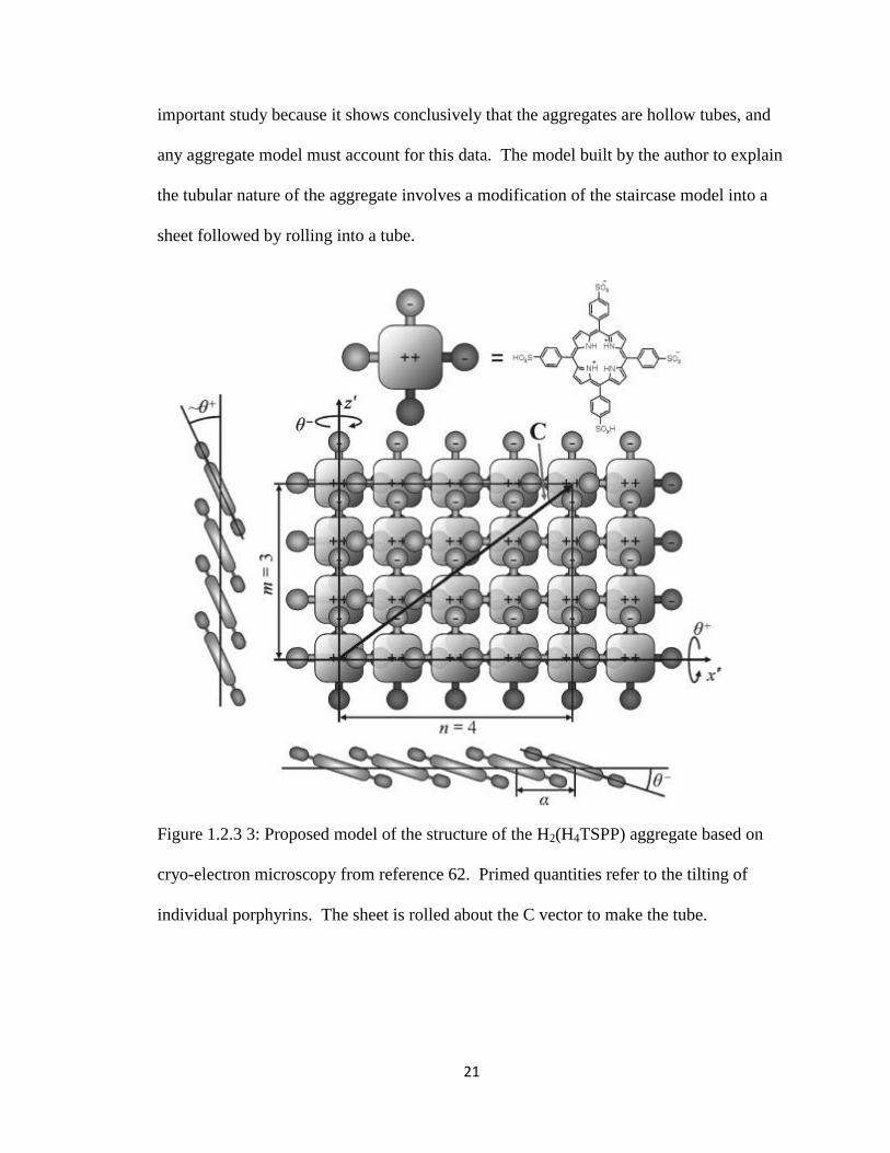
21
important study because it shows conclusively that the aggregates are hollow tubes, and
any aggregate model must account for this data. The model built by the author to explain
the tubular nature of the aggregate involves a modification of the staircase model into a
sheet followed by rolling into a tube.
Figure 1.2.3 3: Proposed model of the structure of the H2(H4TSPP) aggregate based on
cryo-electron microscopy from reference 62. Primed quantities refer to the tilting of
individual porphyrins. The sheet is rolled about the C vector to make the tube.
22
This aggregate model predicts two absorption bands, one polarized perpendicular to the
long axis of the aggregate and one polarized parallel to the long axis which were
confirmed by linear dichroism spectra.62,72
The C, or rolling, vector in this model is
predicted to be a chiral vector, which accounts for reported aggregate chirality.72,101
A
weakness of this model is its density. There are four hydrogens associated with each
porphyrin macrocyle which could be sterically unfavorable.
Fluorescence microscopy studies of H2(H4TSPP) in solution by Kitahama et al.
report long, thin aggregates ranging in length from 4 – 20 µm along the long axis; the
short axis was not discussed.103
The aggregates are susceptible to magnetic fields;
application of a 10 T field caused the aggregates to orient themselves parallel to the
magnetic field. Polarized absorption spectra of the aggregate in the field showed that the
490 and 707 nm absorbance bands are oriented along the long axis of the aggregate,
while the 424 nm band is polarized perpendicular to the long axis. Based upon the
fluorescence microscopy, polarized absorption spectra, and magnetic susceptibility data
the author proposed the following models for the aggregate‟s structure:
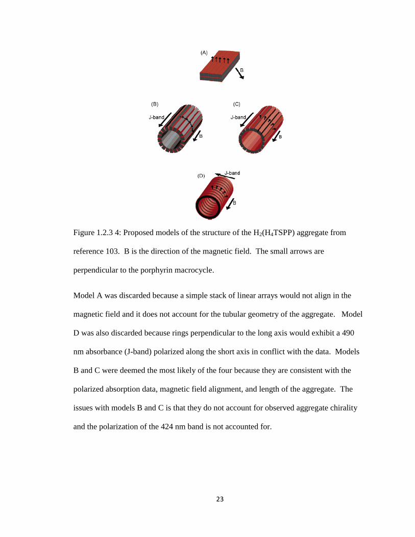
23
Figure 1.2.3 4: Proposed models of the structure of the H2(H4TSPP) aggregate from
reference 103. B is the direction of the magnetic field. The small arrows are
perpendicular to the porphyrin macrocycle.
Model A was discarded because a simple stack of linear arrays would not align in the
magnetic field and it does not account for the tubular geometry of the aggregate. Model
D was also discarded because rings perpendicular to the long axis would exhibit a 490
nm absorbance (J-band) polarized along the short axis in conflict with the data. Models
B and C were deemed the most likely of the four because they are consistent with the
polarized absorption data, magnetic field alignment, and length of the aggregate. The
issues with models B and C is that they do not account for observed aggregate chirality
and the polarization of the 424 nm band is not accounted for.
24
With these two solution models in hand we now turn to solid phase microscopy
studies of H2(H4TSPP) aggregates. Quality AFM and STM data of H2(H4TSPP)
aggregates is scarce. AFM images have been reported for H2(H4TSPP) aggregates
deposited on a number of substrates: mica51,73
, glass51,67,73,105
, HOPG51,58,73
, polystyrene51
,
and silicon.73,105
In accordance with the cryo-electron microscopy and fluorescence
microscopy data AFM and STM images show that the H2(H4TSPP) aggregates are rod-
like. Due to their shape the aggregates are often referred to as “nanorods” or “nanotubes”.
Rod widths range from 20-50 nm, heights 2-4 nm, and lengths range up to several
microns. Several of the dimensions reported in the literature are summarized in Table
1.2.3 1.
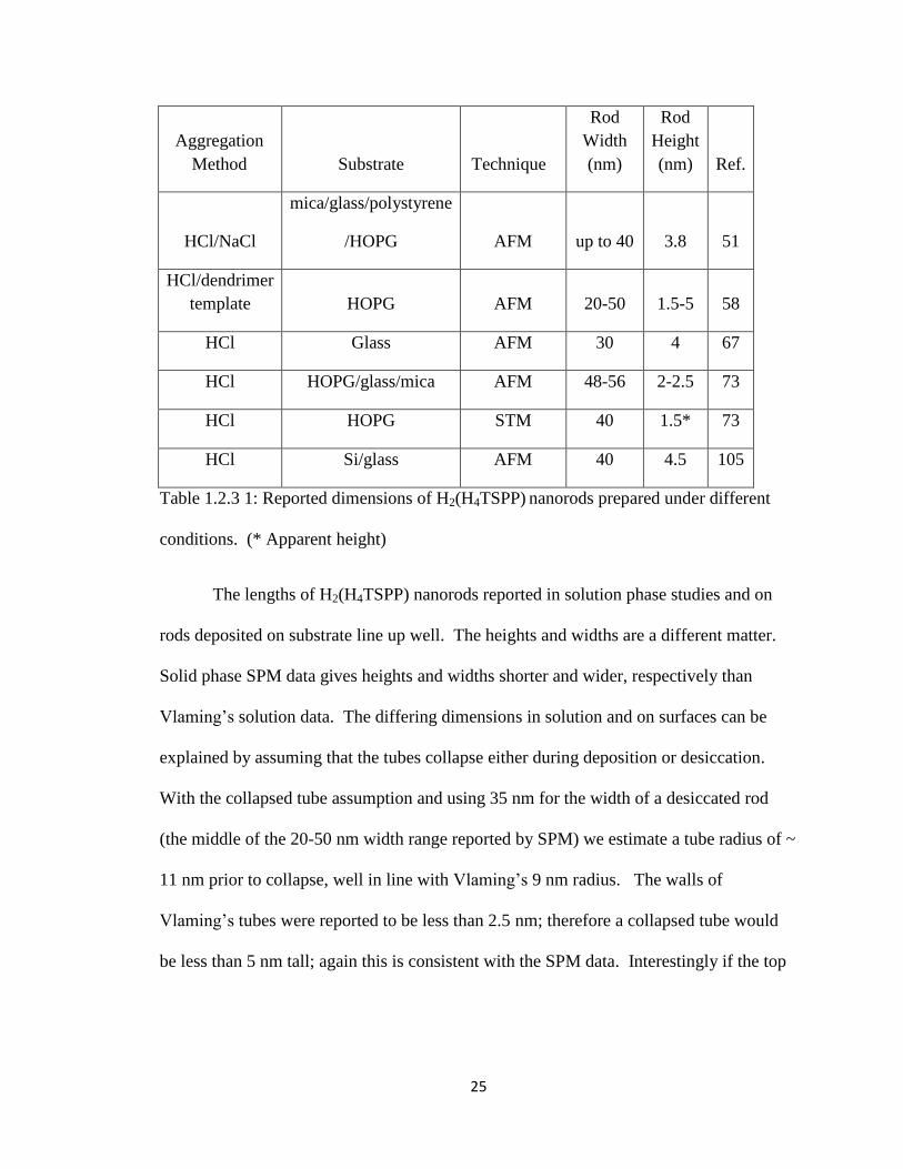
25
Aggregation
Method Substrate Technique
Rod
Width
(nm)
Rod
Height
(nm) Ref.
HCl/NaCl
mica/glass/polystyrene
/HOPG AFM up to 40 3.8 51
HCl/dendrimer
template HOPG AFM 20-50 1.5-5 58
HCl Glass AFM 30 4 67
HCl HOPG/glass/mica AFM 48-56 2-2.5 73
HCl HOPG STM 40 1.5* 73
HCl Si/glass AFM 40 4.5 105
Table 1.2.3 1: Reported dimensions of H2(H4TSPP) nanorods prepared under different
conditions. (* Apparent height)
The lengths of H2(H4TSPP) nanorods reported in solution phase studies and on
rods deposited on substrate line up well. The heights and widths are a different matter.
Solid phase SPM data gives heights and widths shorter and wider, respectively than
Vlaming‟s solution data. The differing dimensions in solution and on surfaces can be
explained by assuming that the tubes collapse either during deposition or desiccation.
With the collapsed tube assumption and using 35 nm for the width of a desiccated rod
(the middle of the 20-50 nm width range reported by SPM) we estimate a tube radius of ~
11 nm prior to collapse, well in line with Vlaming‟s 9 nm radius. The walls of
Vlaming‟s tubes were reported to be less than 2.5 nm; therefore a collapsed tube would
be less than 5 nm tall; again this is consistent with the SPM data. Interestingly if the top
26
half of a collapsed tube was removed a structure ~2 nm tall would result which is close to
the shorter heights reported by SPM.
Intimately coupled with the structure of the nanorods are the electronic properties
of the aggregate. Porphyrin materials in general are known to be photoconductors108
as
well as photovoltaics109
and capable of light-induced charging.110
There has been little
reported in terms of the conducting properties of their self-assembled nanostructures.
Reduction potentials have been reported for monomeric and aggregated H2(H4TSPP) vs.
a normal hydrogen electrode.65
Cyclic voltammetry of monomeric H2(H4TSPP) in
sodium acetate buffer shows a reversible reduction peak at E1/2 = -0.29 V. Aggregated
H2(H4TSPP) in sodium acetate buffer showed a reversible reduction peak at E1/2 = -
0.22V. When deposited on indium tin oxide glass under acetonitrile the aggregate
exhibited two reductions; E1/2 = 0.6 V (reversible) and E1/2 = 0.3 V (irreversible).
Schwab and co-workers49,111
have reported on the photoconductivity of nanorods formed
from highly acidic solutions of H2(H4TSPP). They found that the photoconductivity
grows over hundreds of seconds upon light exposure and decays slowly when the light is
turned off. A qualitative model was proposed where conduction occurred through the
LUMOs of the molecules. They also reported that the rods were insulating over the
voltage range studied (∓0.5 V) in the dark. The same group reported similar current
voltage behavior in nanorods formed from meso-Tri(4-sulfonatophenyl)
monophenylporphine112
(this molecule is the same as H2(H4TSPP) minus one sulfonato
group). In contrast Otsuka et al. reported ohmic behavior for H2(H4TSPP) in the absence
of illumination.113
It should be noted that the device fabrication and nanorod deposition
27
employed by the two groups was very different. Schwab deposited nanorods on the
finished device while Otsuka‟s nanorod deposition was done during device fabrication.
Rubires et al.114
have investigated the effects of water vapor pressure (PH2O) on
H2(H4TSPP) aggregates deposited on a comb-shape microelectrode. Over a bias range of
±100 mV the aggregates were insulating if PH2O < 8 Torr. Above PH2O = 8 Torr a linear
I(V) response was seen, the magnitude of which increased with increasing water vapor
pressure. The group reported high levels of hysteresis in their measurements which were
attributed to capacitance in the aggregate.
The H2(H4TSPP) nanotube system is interesting and important because the
aggregate exhibits properties which are either different from or lacking in the monomer.
For example the nanotubes produce RLS signals while the monomer does not, the tubes
are chiral unlike the monomer; the tubes have different electronic properties than the
monomer, etc. The potential of this aggregate system is quite broad, both as a synthetic
analog of bacterial light harvesting complexes and as a model with which we can study
the fundamentals of self-assembled supramolecular aggregation. Our study of the
H2(H4TSPP) aggregation system has nine goals.
1. To measure solution UV-visible and RLS spectra of monomeric H2(H4TSPP) and it‟s
aggregate to verify the aggregation of H2(H4TSPP) and to parse the electronic
spectrum into monomeric and aggregate components. We will also deposit the
aggregate on glass slides in order to investigate the effects of deposition and
desiccation on the tubes.
28
2. To conduct AFM studies on H2(H4TSPP) nanotubes deposited on substrates to
characterize the dimensions of the tubes.
3. To conduct STM studies on both monomeric H2(H4TSPP) and it‟s aggregate in order
to test the validity of the proposed aggregation models.
4. To carry out Raman studies of the H2(H4TSPP) monomer and nanotubes in solution
to investigate the effects of aggregation on the vibrational structure of the system.
We will also report Raman spectra of nanotubes deposited on Au(111) and compare
with solution data.
5. To conduct compositional testing on the deposited monomer and aggregate by XPS.
6. To conduct the first reported STM I(V) study of both the monomer and aggregate to
investigate the effects of aggregation on the electronic structure of the system. Save
Otsuka et al. the I(V) studies covered in the review were all constrained to bias
voltages less than one volt. We will report on the I(V) characteristics of monomeric
H2(H4TSPP) and it‟s aggregate over a range of ±2 V.
7. To deposit the nanotubes on an interdigitated electrode and measure the conductivity
of the aggregates across the long axis of the tubes over a range of ±2 V.
8. To conduct the first reported HIM studies on H2(H4TSPP) nanotubes in order to test
the validity of the proposed aggregation models.
9. To conduct TEM studies H2(H4TSPP) nanotubes in order to test the validity of the
proposed aggregation models.
Each of these nine objectives will further our understanding of H2(H4TSPP) aggregates
specifically and our understanding of the fundamentals of supramolecular aggregation in
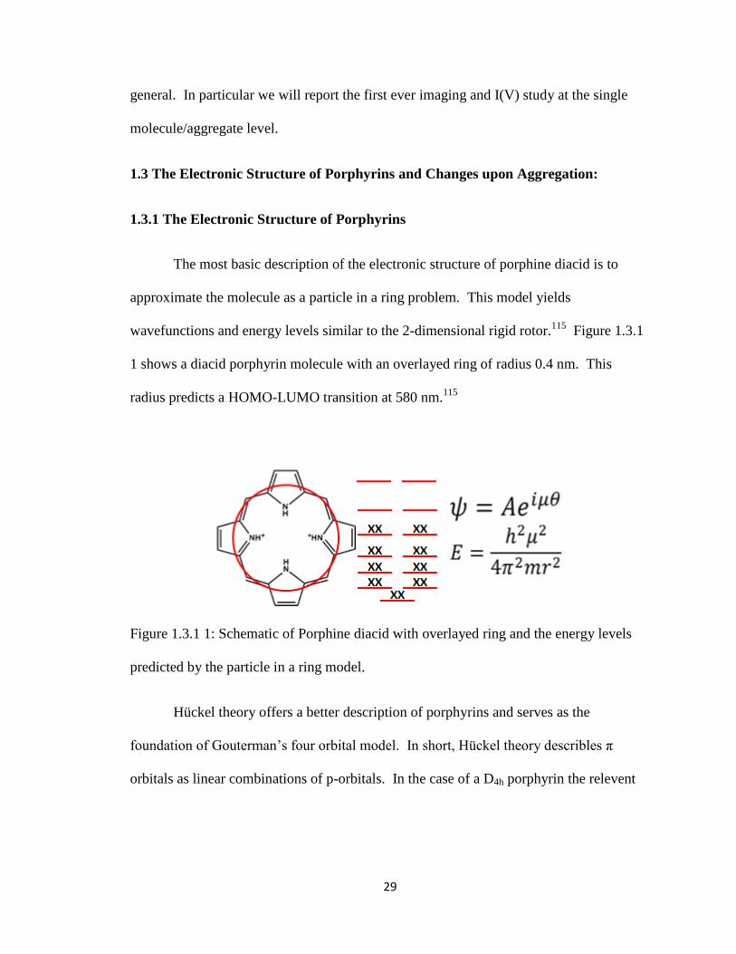
29
general. In particular we will report the first ever imaging and I(V) study at the single
molecule/aggregate level.
1.3 The Electronic Structure of Porphyrins and Changes upon Aggregation:
1.3.1 The Electronic Structure of Porphyrins
The most basic description of the electronic structure of porphine diacid is to
approximate the molecule as a particle in a ring problem. This model yields
wavefunctions and energy levels similar to the 2-dimensional rigid rotor.115
Figure 1.3.1
1 shows a diacid porphyrin molecule with an overlayed ring of radius 0.4 nm. This
radius predicts a HOMO-LUMO transition at 580 nm.115
Figure 1.3.1 1: Schematic of Porphine diacid with overlayed ring and the energy levels
predicted by the particle in a ring model.
Hückel theory offers a better description of porphyrins and serves as the
foundation of Gouterman‟s four orbital model. In short, Hückel theory describles π
orbitals as linear combinations of p-orbitals. In the case of a D4h porphyrin the relevent
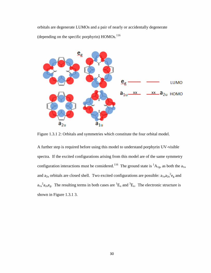
30
orbitals are degenerate LUMOs and a pair of nearly or accidentally degenerate
(depending on the specific porphyrin) HOMOs.116
Figure 1.3.1 2: Orbitals and symmetries which constitute the four orbital model.
A further step is required before using this model to understand porphyrin UV-visible
spectra. If the excited configurations arising from this model are of the same symmetry
configuration interactions must be considered.116
The ground state is 1A1g, as both the a1u
and a2u orbitals are closed shell. Two excited configurations are possible: a1ua2u2eg and
a1u2a2ueg. The resulting terms in both cases are
1Eu and
3Eu. The electronic structure is
shown in Figure 1.3.1 3.
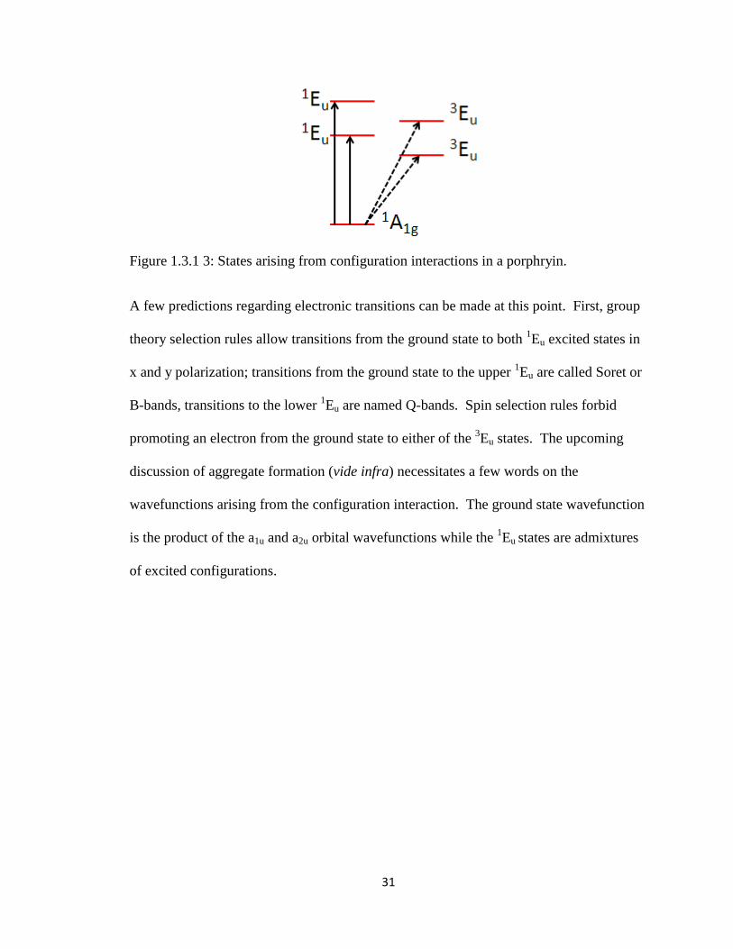
31
Figure 1.3.1 3: States arising from configuration interactions in a porphryin.
A few predictions regarding electronic transitions can be made at this point. First, group
theory selection rules allow transitions from the ground state to both 1Eu excited states in
x and y polarization; transitions from the ground state to the upper 1Eu are called Soret or
B-bands, transitions to the lower 1Eu are named Q-bands. Spin selection rules forbid
promoting an electron from the ground state to either of the 3Eu states. The upcoming
discussion of aggregate formation (vide infra) necessitates a few words on the
wavefunctions arising from the configuration interaction. The ground state wavefunction
is the product of the a1u and a2u orbital wavefunctions while the 1Eu states are admixtures
of excited configurations.
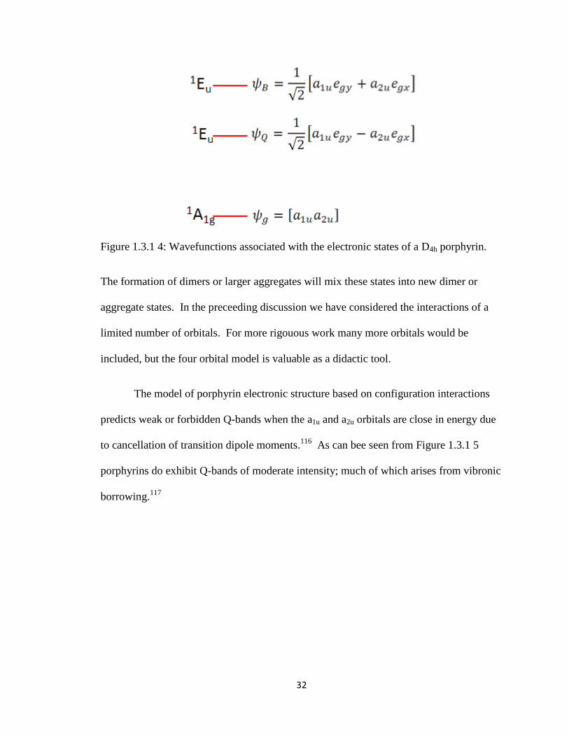
32
Figure 1.3.1 4: Wavefunctions associated with the electronic states of a D4h porphyrin.
The formation of dimers or larger aggregates will mix these states into new dimer or
aggregate states. In the preceeding discussion we have considered the interactions of a
limited number of orbitals. For more rigouous work many more orbitals would be
included, but the four orbital model is valuable as a didactic tool.
The model of porphyrin electronic structure based on configuration interactions
predicts weak or forbidden Q-bands when the a1u and a2u orbitals are close in energy due
to cancellation of transition dipole moments.116
As can bee seen from Figure 1.3.1 5
porphyrins do exhibit Q-bands of moderate intensity; much of which arises from vibronic
borrowing.117
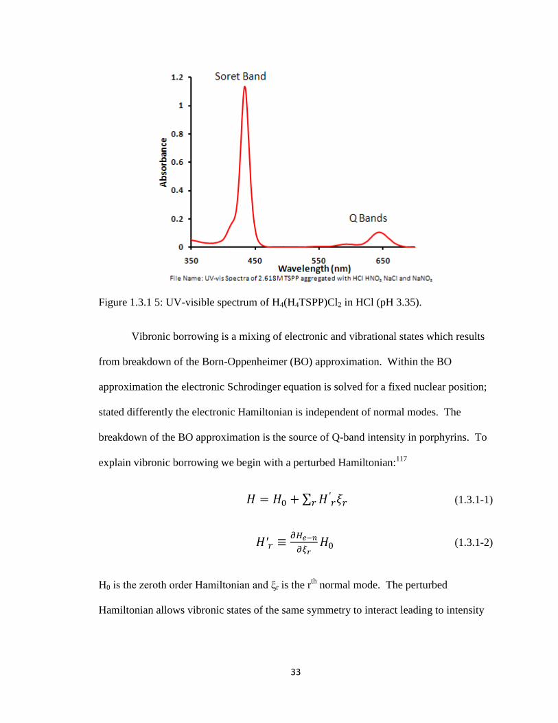
33
Figure 1.3.1 5: UV-visible spectrum of H4(H4TSPP)Cl2 in HCl (pH 3.35).
Vibronic borrowing is a mixing of electronic and vibrational states which results
from breakdown of the Born-Oppenheimer (BO) approximation. Within the BO
approximation the electronic Schrodinger equation is solved for a fixed nuclear position;
stated differently the electronic Hamiltonian is independent of normal modes. The
breakdown of the BO approximation is the source of Q-band intensity in porphyrins. To
explain vibronic borrowing we begin with a perturbed Hamiltonian:117
(1.3.1-1)
(1.3.1-2)
H0 is the zeroth order Hamiltonian and ξr is the rth
normal mode. The perturbed
Hamiltonian allows vibronic states of the same symmetry to interact leading to intensity
34
borrowing. The operator transforms as the totally symmetric irreducible representation
so the derivative and the normal mode must be of the same symmetry in order to interact.
The mixing of vibronic states yields wavefunctions of the form:
(1.3.1-3)
Capital letters denote electronic states, lower case letters denote vibrational states, and a
superscripted zero indicates equilibrium geometry. K is the state to which the Q state is
coupling. The sum runs over all normal coordinates and vibronic states. The degree to
which Q interacts with other states is governed by a number of factors. If the energetic
separation between the two states is large (high ΔE) they will not couple strongly. The
operator H‟r transforms as the totally symmetric irreducible representation so the matrix
element will vanish if K and Qx belong to different irreducible
representations. ξr can connect vibrational states which differ by one quantum, otherwise
the integral will vanish and the states will not mix. With the wavefunction in hand we can
discuss the intensity of the Q-bands.
(1.3.1-4)
Where E is the electric dipole moment operator. As was discussed earlier the transition
dipole moment for matrix element is zero due to cancelation. The terms
in the summation show that Q-band gains intensity by mixing with electric dipole
allowed states of the same symmetry. Equation 1.3.1-4 predicts that the lower 1Eu state
(Q) will couple with the upper 1Eu state (Soret) and gain intensity.
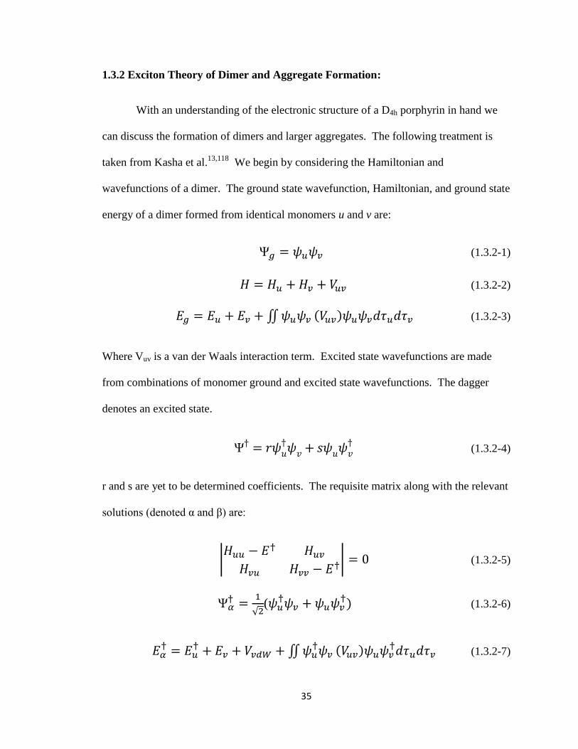
35
1.3.2 Exciton Theory of Dimer and Aggregate Formation:
With an understanding of the electronic structure of a D4h porphyrin in hand we
can discuss the formation of dimers and larger aggregates. The following treatment is
taken from Kasha et al.13,118
We begin by considering the Hamiltonian and
wavefunctions of a dimer. The ground state wavefunction, Hamiltonian, and ground state
energy of a dimer formed from identical monomers u and v are:
(1.3.2-1)
(1.3.2-2)
(1.3.2-3)
Where Vuv is a van der Waals interaction term. Excited state wavefunctions are made
from combinations of monomer ground and excited state wavefunctions. The dagger
denotes an excited state.
(1.3.2-4)
r and s are yet to be determined coefficients. The requisite matrix along with the relevant
solutions (denoted α and β) are:
(1.3.2-5)
(
(1.3.2-6)
(1.3.2-7)
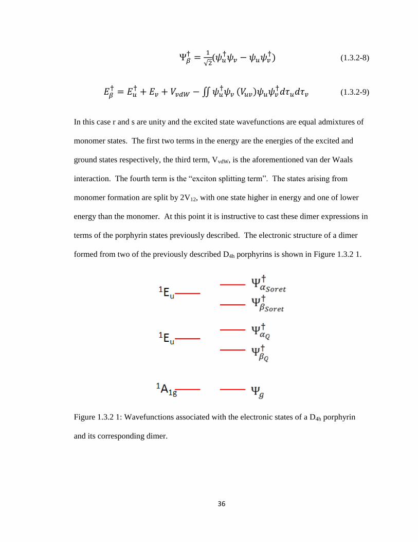
36
(
(1.3.2-8)
(1.3.2-9)
In this case r and s are unity and the excited state wavefunctions are equal admixtures of
monomer states. The first two terms in the energy are the energies of the excited and
ground states respectively, the third term, VvdW, is the aforementioned van der Waals
interaction. The fourth term is the “exciton splitting term”. The states arising from
monomer formation are split by 2V12, with one state higher in energy and one of lower
energy than the monomer. At this point it is instructive to cast these dimer expressions in
terms of the porphyrin states previously described. The electronic structure of a dimer
formed from two of the previously described D4h porphyrins is shown in Figure 1.3.2 1.
Figure 1.3.2 1: Wavefunctions associated with the electronic states of a D4h porphyrin
and its corresponding dimer.
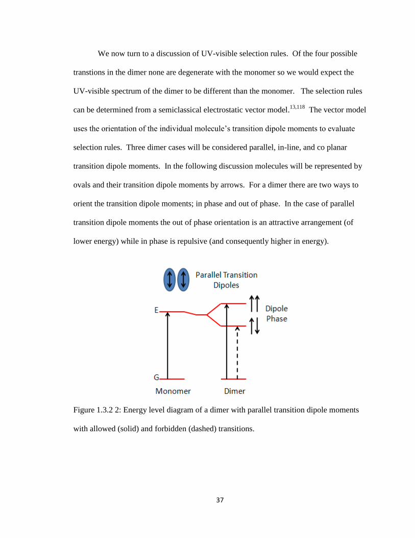
37
We now turn to a discussion of UV-visible selection rules. Of the four possible
transtions in the dimer none are degenerate with the monomer so we would expect the
UV-visible spectrum of the dimer to be different than the monomer. The selection rules
can be determined from a semiclassical electrostatic vector model.13,118
The vector model
uses the orientation of the individual molecule‟s transition dipole moments to evaluate
selection rules. Three dimer cases will be considered parallel, in-line, and co planar
transition dipole moments. In the following discussion molecules will be represented by
ovals and their transition dipole moments by arrows. For a dimer there are two ways to
orient the transition dipole moments; in phase and out of phase. In the case of parallel
transition dipole moments the out of phase orientation is an attractive arrangement (of
lower energy) while in phase is repulsive (and consequently higher in energy).
Figure 1.3.2 2: Energy level diagram of a dimer with parallel transition dipole moments
with allowed (solid) and forbidden (dashed) transitions.
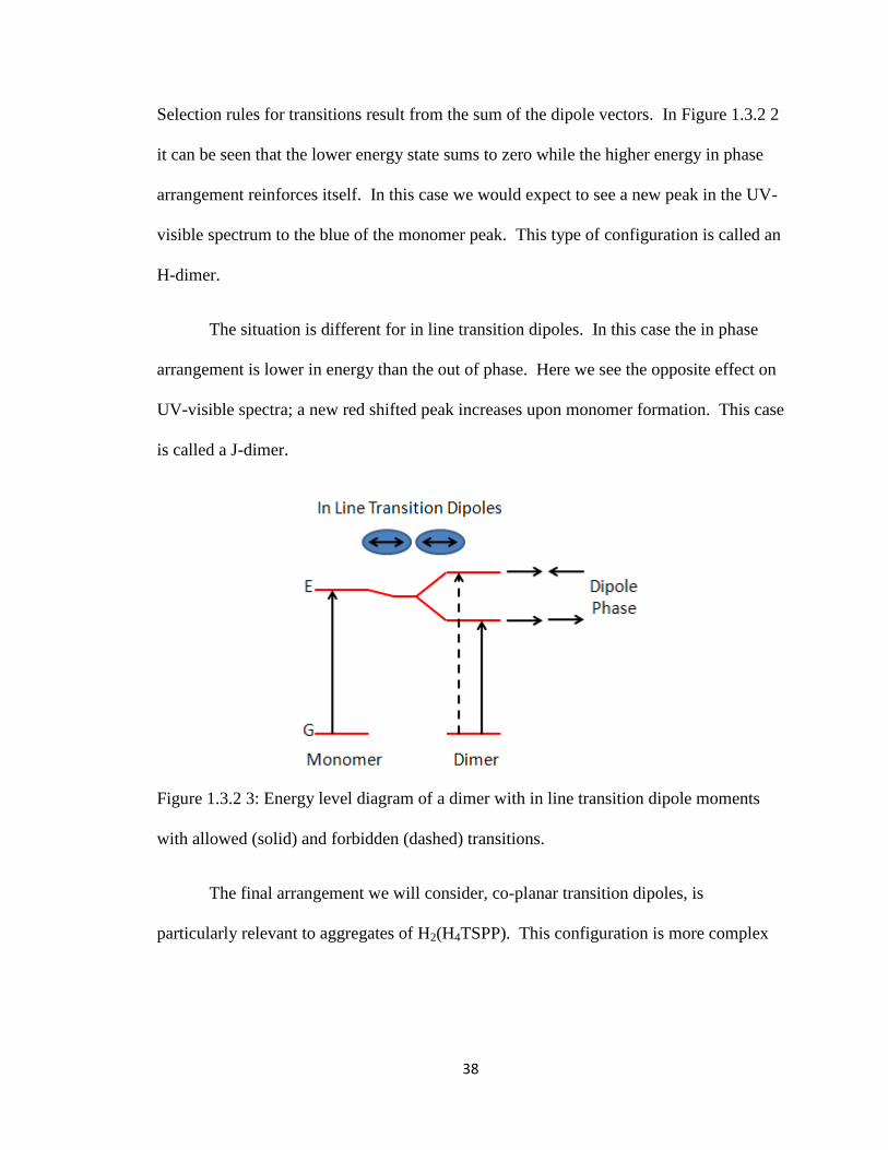
38
Selection rules for transitions result from the sum of the dipole vectors. In Figure 1.3.2 2
it can be seen that the lower energy state sums to zero while the higher energy in phase
arrangement reinforces itself. In this case we would expect to see a new peak in the UV-
visible spectrum to the blue of the monomer peak. This type of configuration is called an
H-dimer.
The situation is different for in line transition dipoles. In this case the in phase
arrangement is lower in energy than the out of phase. Here we see the opposite effect on
UV-visible spectra; a new red shifted peak increases upon monomer formation. This case
is called a J-dimer.
Figure 1.3.2 3: Energy level diagram of a dimer with in line transition dipole moments
with allowed (solid) and forbidden (dashed) transitions.
The final arrangement we will consider, co-planar transition dipoles, is
particularly relevant to aggregates of H2(H4TSPP). This configuration is more complex
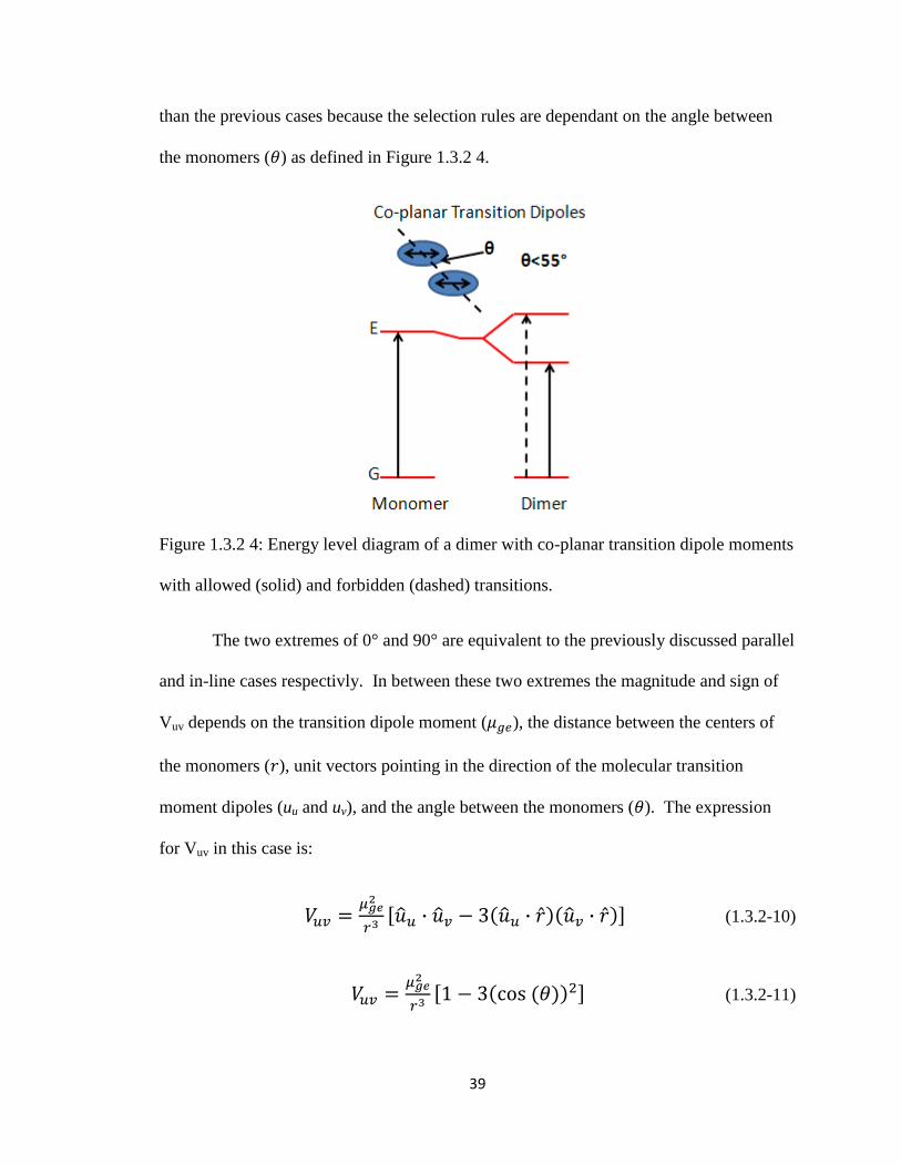
39
than the previous cases because the selection rules are dependant on the angle between
the monomers ( ) as defined in Figure 1.3.2 4.
Figure 1.3.2 4: Energy level diagram of a dimer with co-planar transition dipole moments
with allowed (solid) and forbidden (dashed) transitions.
The two extremes of 0° and 90° are equivalent to the previously discussed parallel
and in-line cases respectivly. In between these two extremes the magnitude and sign of
Vuv depends on the transition dipole moment ( ), the distance between the centers of
the monomers ( ), unit vectors pointing in the direction of the molecular transition
moment dipoles (uu and uv), and the angle between the monomers ( ). The expression
for Vuv in this case is:
(1.3.2-10)
(1.3.2-11)
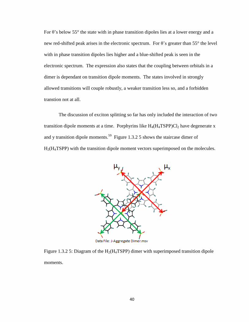
40
For θ‟s below 55° the state with in phase transition dipoles lies at a lower energy and a
new red-shifted peak arises in the electronic spectrum. For θ‟s greater than 55° the level
with in phase transition dipoles lies higher and a blue-shifted peak is seen in the
electronic spectrum. The expression also states that the coupling between orbitals in a
dimer is dependant on transition dipole moments. The states involved in strongly
allowed transitions will couple robustly, a weaker transition less so, and a forbidden
transtion not at all.
The discussion of exciton splitting so far has only included the interaction of two
transition dipole moments at a time. Porphyrins like H4(H4TSPP)Cl2 have degenerate x
and y transition dipole moments.59
Figure 1.3.2 5 shows the staircase dimer of
H2(H4TSPP) with the transition dipole moment vectors superimposed on the molecules.
Figure 1.3.2 5: Diagram of the H2(H4TSPP) dimer with superimposed transition dipole
moments.

41
The model in Figure 1.3.2 5 predicts two new peaks in the UV-visible spectrum upon
aggregation. The µx transition dipoles on the constituent monomers couple as in the co-
planar example with a predicted red-shifted peak. The µy transition dipoles on the
constituent monomers couple as in the parallel transition dipole moment example with a
predicted blue-shifted peak. µx and µy are orthogonal so no coupling occurs for these two
dipoles. The terms J-dimer or H-dimer do not describe the coupling of H2(H4TSPP)
monomers well. The H2(H4TSPP) dimer geometery is such that both types of coupling
are expected.
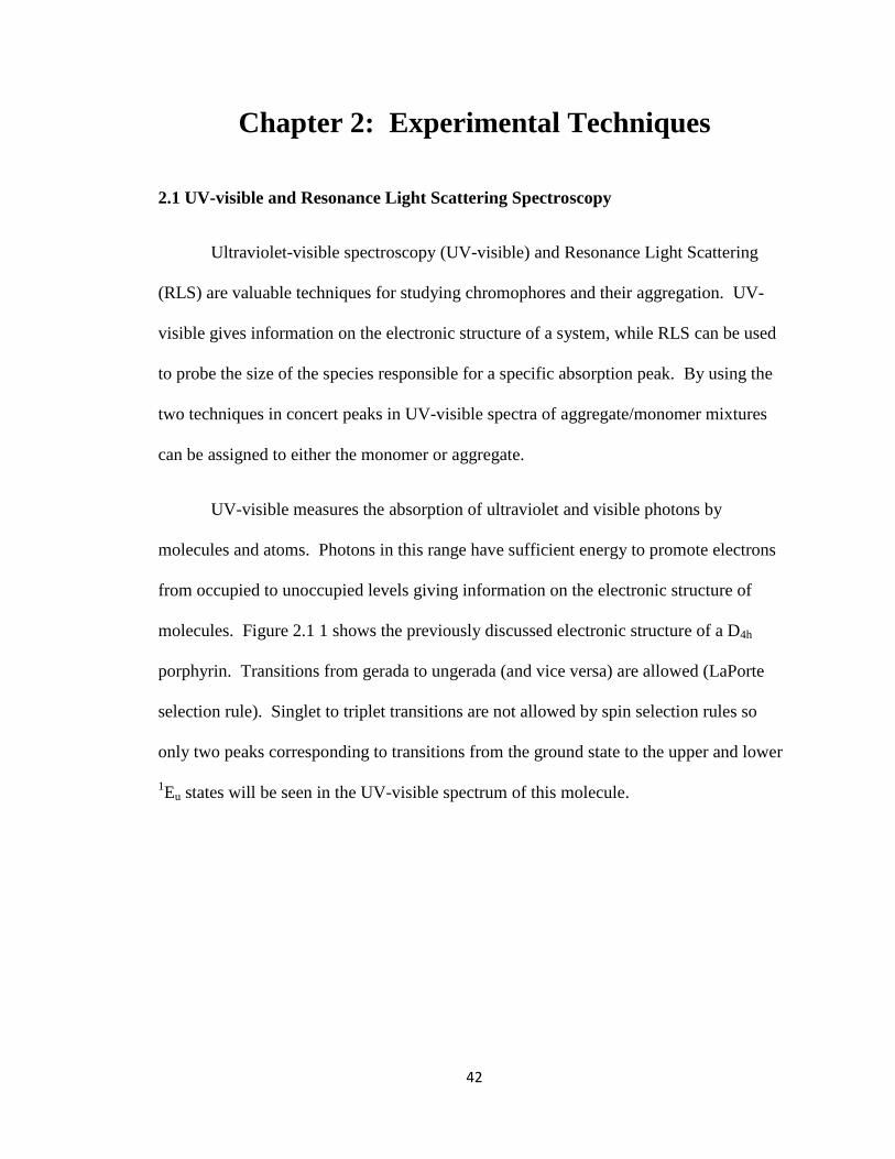
42
Chapter 2: Experimental Techniques
2.1 UV-visible and Resonance Light Scattering Spectroscopy
Ultraviolet-visible spectroscopy (UV-visible) and Resonance Light Scattering
(RLS) are valuable techniques for studying chromophores and their aggregation. UV-
visible gives information on the electronic structure of a system, while RLS can be used
to probe the size of the species responsible for a specific absorption peak. By using the
two techniques in concert peaks in UV-visible spectra of aggregate/monomer mixtures
can be assigned to either the monomer or aggregate.
UV-visible measures the absorption of ultraviolet and visible photons by
molecules and atoms. Photons in this range have sufficient energy to promote electrons
from occupied to unoccupied levels giving information on the electronic structure of
molecules. Figure 2.1 1 shows the previously discussed electronic structure of a D4h
porphyrin. Transitions from gerada to ungerada (and vice versa) are allowed (LaPorte
selection rule). Singlet to triplet transitions are not allowed by spin selection rules so
only two peaks corresponding to transitions from the ground state to the upper and lower
1Eu states will be seen in the UV-visible spectrum of this molecule.
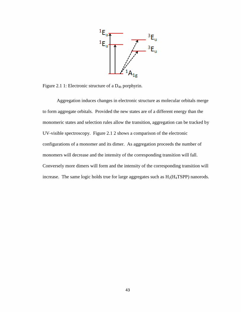
43
Figure 2.1 1: Electronic structure of a D4h porphyrin.
Aggregation induces changes in electronic structure as molecular orbitals merge
to form aggregate orbitals. Provided the new states are of a different energy than the
monomeric states and selection rules allow the transition, aggregation can be tracked by
UV-visible spectroscopy. Figure 2.1 2 shows a comparison of the electronic
configurations of a monomer and its dimer. As aggregation proceeds the number of
monomers will decrease and the intensity of the corresponding transition will fall.
Conversely more dimers will form and the intensity of the corresponding transition will
increase. The same logic holds true for large aggregates such as H2(H4TSPP) nanorods.
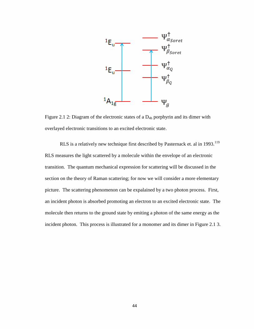
44
Figure 2.1 2: Diagram of the electronic states of a D4h porphyrin and its dimer with
overlayed electronic transitions to an excited electronic state.
RLS is a relatively new technique first described by Pasternack et. al in 1993.119
RLS measures the light scattered by a molecule within the envelope of an electronic
transition. The quantum mechanical expression for scattering will be discussed in the
section on the theory of Raman scattering; for now we will consider a more elementary
picture. The scattering phenomenon can be expalained by a two photon process. First,
an incident photon is absorbed promoting an electron to an excited electronic state. The
molecule then returns to the ground state by emiting a photon of the same energy as the
incident photon. This process is illustrated for a monomer and its dimer in Figure 2.1 3.
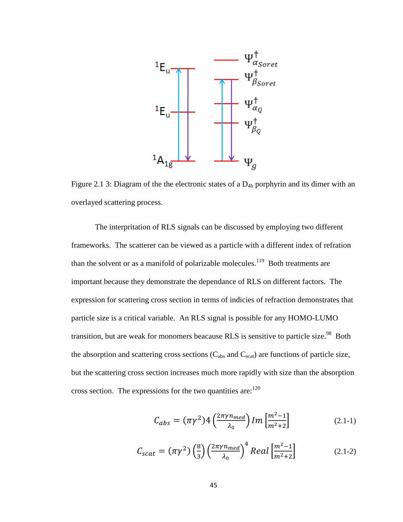
45
Figure 2.1 3: Diagram of the the electronic states of a D4h porphyrin and its dimer with an
overlayed scattering process.
The interpritation of RLS signals can be discussed by employing two different
frameworks. The scatterer can be viewed as a particle with a different index of refration
than the solvent or as a manifold of polarizable molecules.119
Both treatments are
important because they demonstrate the dependance of RLS on different factors. The
expression for scattering cross section in terms of indicies of refraction demonstrates that
particle size is a critical variable. An RLS signal is possible for any HOMO-LUMO
transition, but are weak for monomers beacause RLS is sensitive to particle size.98
Both
the absorption and scattering cross sections (Cabs and Cscat) are functions of particle size,
but the scattering cross section increases much more rapidly with size than the absorption
cross section. The expressions for the two quantities are:120
(2.1-1)
(2.1-2)
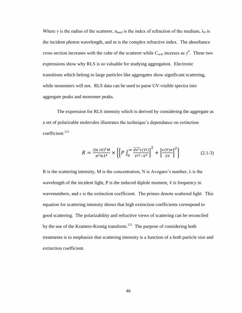
46
Where γ is the radius of the scatterer, nmed is the index of refraction of the medium, λ0 is
the incident photon wavelength, and m is the complex refractive index. The absorbance
cross section increases with the cube of the scatterer while Cscat increses as γ6. These two
expressions show why RLS is so valuable for studying aggregation. Electronic
transitions which belong to large particles like aggregates show significant scattering,
while monomers will not. RLS data can be used to parse UV-visible spectra into
aggregate peaks and monomer peaks.
The expression for RLS intensity which is derived by considering the aggregate as
a set of polarizable molecules illustrates the technique‟s dependance on extinction
coefficient:121
(2.1-3)
R is the scattering intensity, M is the concentration, N is Avogaro‟s number, λ is the
wavelength of the incident light, P is the induced diplole moment, is frequency in
wavenumbers, and ε is the extinction coefficient. The primes denote scattered light. This
equation for scattering intensity shows that high extinction coefficients correspond to
good scattering. The polarizability and refractive views of scattering can be reconciled
by the use of the Kramers-Kronig transform.121
The purpose of considering both
treatments is to emphasize that scattering intensity is a function of a both particle size and
extinction coefficient.
47
As an example of the utility of RLS scattering data for the H2(H4TSPP) monomer
and aggregate is presented in Figure 2.1 4. The monomer spectrum has a dip at ~ 430 nm
corresponding to the Soret band of the monomer. For particles the size of monomeric
H2(H4TSPP) absorbance dominates over scattering. The opposite is true for the
aggregate. The aggregate RLS spectrum shows a strong peak at ~ 490 nm corresponding
to the aggregate Soret band. A dip in the spectrum is visible just to the blue of the
scattering peak indicates that both scattering and absorption are occuring, but clearly
scattering is the dominant process. The raw intensities of the two spectra are very
different as well. The aggregate RLS spectrum is two orders of magnitude greater than
the monomer spectrum. When graphed on the same axes the monomeric RLS spectrum
looks almost flat.
Figure 2.1 4: RLS spectra of H2(H4TSPP) monomer (0.74 µM H2(H4TSPP) in 0.75 M
HCl, left) and aggregate (5.9 µM H2(H4TSPP) in 0.75 M HCl, right).
48
The last point concerns the Q-bands. Notice the peak at ~ 650 nm in the monomer RLS
spectrum. This peak is fluorescence from the residual monomer Q-band not RLS. An
important weakness of RLS is its inability to discern fluorescence from scattering. What
is referred to as an RLS spectrum is really an emission spectrum. The fluorimeter is
configured to detect photons emitted at 90° to the incident beam irrespective of their
origins. Photons from RLS, fluorescence, and phosphorescence will all appear in the
spectrum so careful interpritation of the spectra are required. For H2(H4TSPP) aggregates
the spectra are relativly easy to interprite because the only non-RLS signal observed is
monomer Q-band fluorescence.
2.2 X-ray and Ultraviolet Photoelectron Spectroscopy
Both X-ray Photoelectron Spectroscopy (XPS) and Ultraviolet Photoelectron
Spectroscopy (UPS) are powerful surface analysis techniques capable of probing the
electronic structure of an analyte. XPS and UPS employ the photoelectric effect
described by Einstein in 1905122
to analyze surfaces and/or adsorbate molecules. X-ray
or ultraviolet photons incident on a sample will eject electrons from that sample with a
range of kinetic energies because x-ray and ultraviolet photons impart sufficient energy
for electrons to overcome nuclear attraction, called binding energy, and escape the
sample. Electrons in the valence shells are held least tightly and are therefore easiest to
remove. Because the mean escape depth of photoelectrons from a surface is ~ 1 nm in
the X-ray region photoelectron spectroscopy only probes 6–10 nm into a sample,123
thus
it is a surface sensitive technique. Ultraviolet Photoelectron Spectroscopy (UPS) is used
to study valence shell electrons as ultraviolet photons (10-45 eV) have sufficient energy
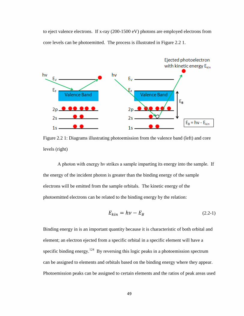
49
to eject valence electrons. If x-ray (200-1500 eV) photons are employed electrons from
core levels can be photoemitted. The process is illustrated in Figure 2.2 1.
Figure 2.2 1: Diagrams illustrating photoemission from the valence band (left) and core
levels (right)
A photon with energy hν strikes a sample imparting its energy into the sample. If
the energy of the incident photon is greater than the binding energy of the sample
electrons will be emitted from the sample orbitals. The kinetic energy of the
photoemitted electrons can be related to the binding energy by the relation:
(2.2-1)
Binding energy in is an important quantity because it is characteristic of both orbital and
element; an electron ejected from a specific orbital in a specific element will have a
specific binding energy.124
By reversing this logic peaks in a photoemission spectrum
can be assigned to elements and orbitals based on the binding energy where they appear.
Photoemission peaks can be assigned to certain elements and the ratios of peak areas used
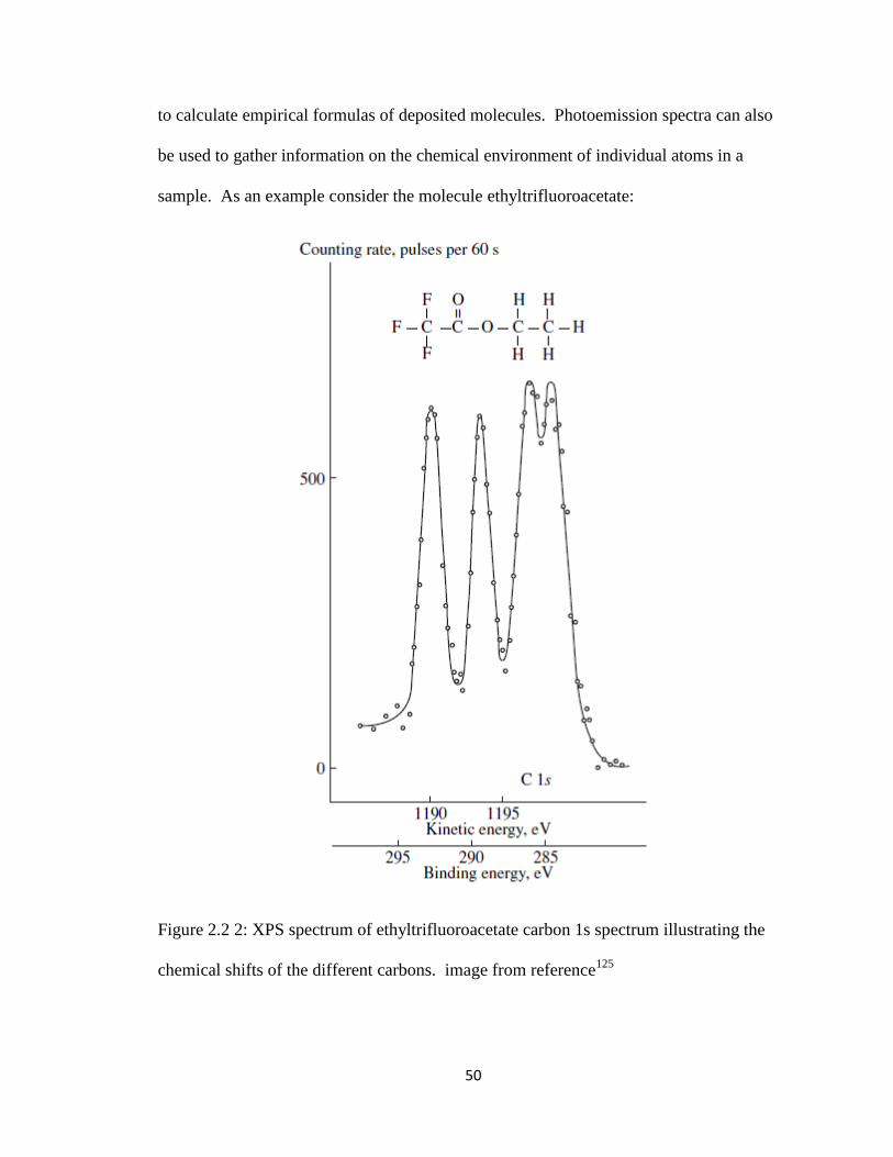
50
to calculate empirical formulas of deposited molecules. Photoemission spectra can also
be used to gather information on the chemical environment of individual atoms in a
sample. As an example consider the molecule ethyltrifluoroacetate:
Figure 2.2 2: XPS spectrum of ethyltrifluoroacetate carbon 1s spectrum illustrating the
chemical shifts of the different carbons. image from reference125
51
The C1s signal in the XPS spectrum of this molecule is split into four separate peaks due
to the differing environments of the carbons.126
Fluorine, with its high electronegativity
strongly withdraws electrons from its attached carbon, making it more difficult to remove
electrons from the fluorinated carbon. Stated differently, electrons in the fluorinated
carbon will have the highest binding energy. Electrons with the next highest binding
energy belong to the ester carbon as oxygen is not as electronegative as fluorine.
Hydrogen is a much less efficient electron withdrawing species than either fluorine or
oxygen so the carbon not bound to fluorine or oxygen will have the lowest binding
energy. This example illustrates how XPS can be used to gather information on the
differing chemical environments of a particular element in a sample. The ratios of the
differing carbons can also be deduced by comparing the peak areas. Not surprisingly in
the case of ethyltrifluoroacetate the ratio is 1:1:1:1. Ethyltrifluoroacetate serves as an
excellent example of the capabilities of XPS in elemental analysis and determining
chemical environment.
UPS is analogous to XPS save that it probes the valence energy levels of the
sample. Photons from a helium discharge lamp with an energy of 21.2 eV124
are used to
irradiate the sample as opposed to X-rays. The ultraviolet photons eject valence electrons
from the sample which are analyzed in a similar fashion to XPS. In addition to
elucidating the energies of valence orbitals UPS can be used to find the workfunction of a
sample. The 21.2 eV HeI photon impinging on the sample imparts its energy into the
sample. In order for the electron to escape the sample and be measured by the detector it
must have sufficient energy to overcome the sample‟s workfunction. The most deeply
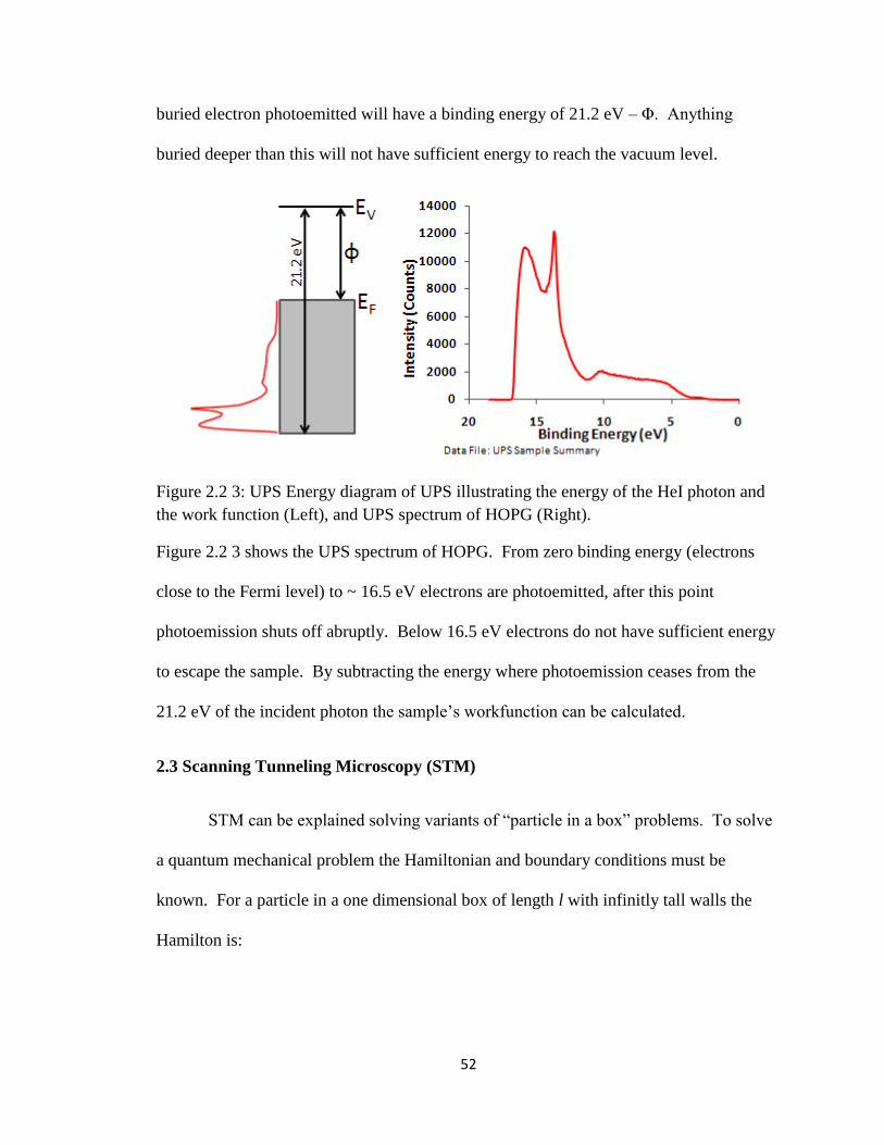
52
buried electron photoemitted will have a binding energy of 21.2 eV – Φ. Anything
buried deeper than this will not have sufficient energy to reach the vacuum level.
Figure 2.2 3: UPS Energy diagram of UPS illustrating the energy of the HeI photon and
the work function (Left), and UPS spectrum of HOPG (Right).
Figure 2.2 3 shows the UPS spectrum of HOPG. From zero binding energy (electrons
close to the Fermi level) to ~ 16.5 eV electrons are photoemitted, after this point
photoemission shuts off abruptly. Below 16.5 eV electrons do not have sufficient energy
to escape the sample. By subtracting the energy where photoemission ceases from the
21.2 eV of the incident photon the sample‟s workfunction can be calculated.
2.3 Scanning Tunneling Microscopy (STM)
STM can be explained solving variants of “particle in a box” problems. To solve
a quantum mechanical problem the Hamiltonian and boundary conditions must be
known. For a particle in a one dimensional box of length l with infinitly tall walls the
Hamilton is:
53
(2.3-1)
Where h is plank‟s constant, m is the mass, q is the coordinate, and is the
wavefunction. In this case there is only one boundary condition; the wavefunction must
vanish at the walls because there is zero probability of the particle being found outside
the box. To find the energies, E, the following differential equation must be solved:
(2.3-2)
(2.3-3)
The solution to this differential equation is well known:
(2.3-4)
The energy levels of the particle are therefore:
(2.3-5)
The next step is a particle in a box with a finite wall of thickness x. The problem is more
tractable if it is broken into three regions:
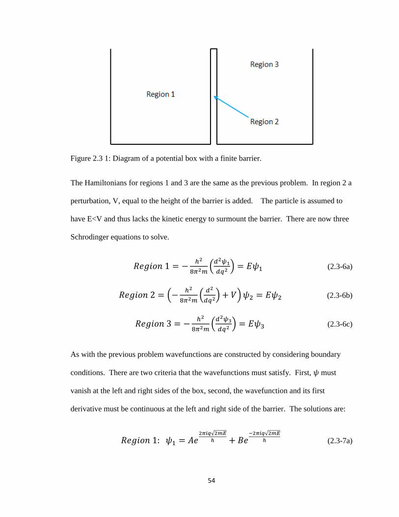
54
Figure 2.3 1: Diagram of a potential box with a finite barrier.
The Hamiltonians for regions 1 and 3 are the same as the previous problem. In region 2 a
perturbation, V, equal to the height of the barrier is added. The particle is assumed to
have E<V and thus lacks the kinetic energy to surmount the barrier. There are now three
Schrodinger equations to solve.
(2.3-6a)
(2.3-6b)
(2.3-6c)
As with the previous problem wavefunctions are constructed by considering boundary
conditions. There are two criteria that the wavefunctions must satisfy. First, must
vanish at the left and right sides of the box, second, the wavefunction and its first
derivative must be continuous at the left and right side of the barrier. The solutions are:
(2.3-7a)
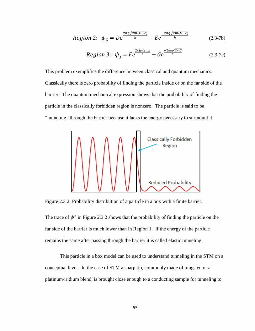
55
(2.3-7b)
(2.3-7c)
This problem exemplifies the difference between classical and quantum mechanics.
Classically there is zero probability of finding the particle inside or on the far side of the
barrier. The quantum mechanical expression shows that the probability of finding the
particle in the classically forbidden region is nonzero. The particle is said to be
“tunneling” through the barrier because it lacks the energy necessary to surmount it.
Figure 2.3 2: Probability distribution of a particle in a box with a finite barrier.
The trace of in Figure 2.3 2 shows that the probability of finding the particle on the
far side of the barrier is much lower than in Region 1. If the energy of the particle
remains the same after passing through the barrier it is called elastic tunneling.
This particle in a box model can be used to understand tunneling in the STM on a
conceptual level. In the case of STM a sharp tip, commonly made of tungsten or a
platinum/iridium blend, is brought close enough to a conducting sample for tunneling to
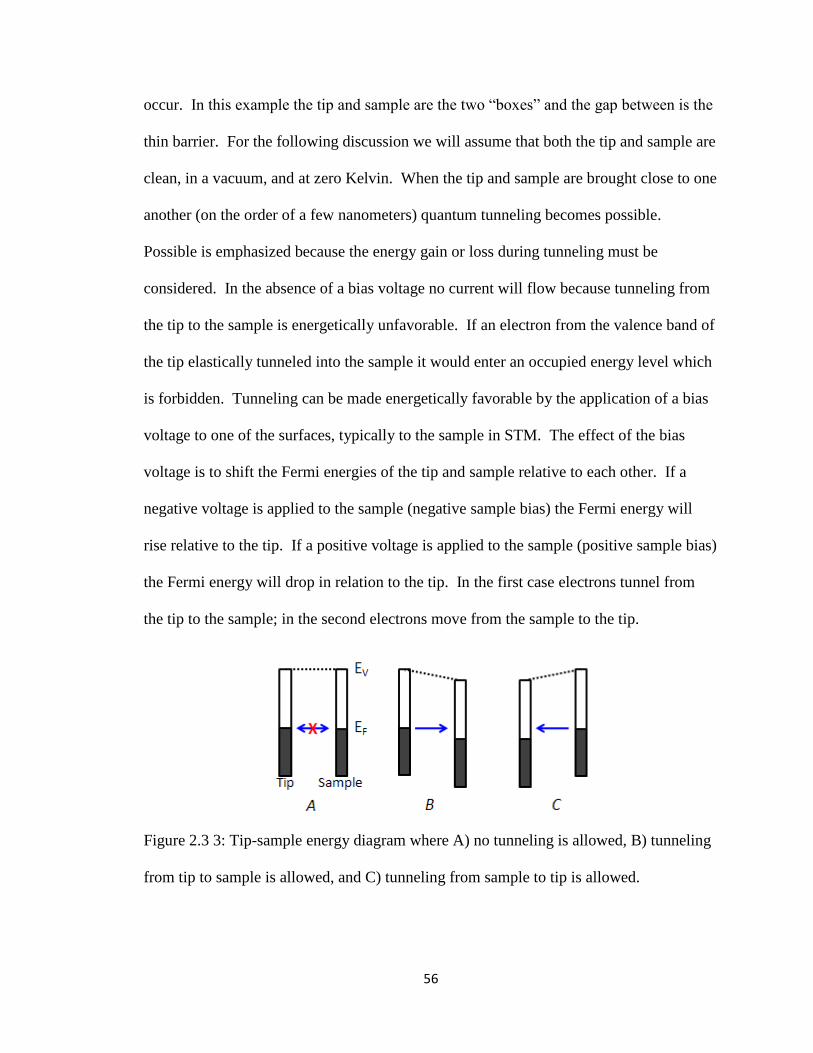
56
occur. In this example the tip and sample are the two “boxes” and the gap between is the
thin barrier. For the following discussion we will assume that both the tip and sample are
clean, in a vacuum, and at zero Kelvin. When the tip and sample are brought close to one
another (on the order of a few nanometers) quantum tunneling becomes possible.
Possible is emphasized because the energy gain or loss during tunneling must be
considered. In the absence of a bias voltage no current will flow because tunneling from
the tip to the sample is energetically unfavorable. If an electron from the valence band of
the tip elastically tunneled into the sample it would enter an occupied energy level which
is forbidden. Tunneling can be made energetically favorable by the application of a bias
voltage to one of the surfaces, typically to the sample in STM. The effect of the bias
voltage is to shift the Fermi energies of the tip and sample relative to each other. If a
negative voltage is applied to the sample (negative sample bias) the Fermi energy will
rise relative to the tip. If a positive voltage is applied to the sample (positive sample bias)
the Fermi energy will drop in relation to the tip. In the first case electrons tunnel from
the tip to the sample; in the second electrons move from the sample to the tip.
Figure 2.3 3: Tip-sample energy diagram where A) no tunneling is allowed, B) tunneling
from tip to sample is allowed, and C) tunneling from sample to tip is allowed.

57
During the STM scan the tip is rastered across the surface to probe the sample‟s
properties. The microscope can be operated in two different modes: constant current and
constant height. In constant current mode a feedback loop modulates the tip-sample
separation to keep a constant tunneling current. In this mode the STM image is a map of
the motion of the tip as it moves over the surface. One of the advantages of this method
is the chance of crashing the tip is minimized, the disadvantage is slow scan speed.
Constant height mode fixes the tip at a particular tip-sample separation during scanning.
The resulting image is a map of tunneling current at each location. The advantage of this
mode is greater scan speed than constant current; the weakness is potentially crashing the
tip while scanning over rough surfaces.
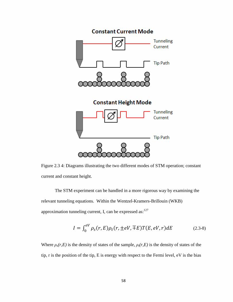
58
Figure 2.3 4: Diagrams illustrating the two different modes of STM operation; constant
current and constant height.
The STM experiment can be handled in a more rigorous way by examining the
relevant tunneling equations. Within the Wentzel-Kramers-Brillouin (WKB)
approximation tunneling current, I, can be expressed as:127
∓
(2.3-8)
Where ρs(r,E) is the density of states of the sample, ρt(r,E) is the density of states of the
tip, r is the position of the tip, E is energy with respect to the Fermi level, eV is the bias
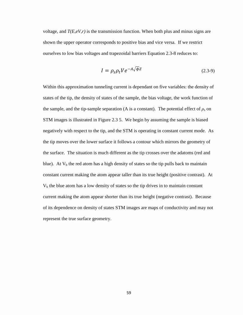
59
voltage, and T(E,eV,r) is the transmission function. When both plus and minus signs are
shown the upper operator corresponds to positive bias and vice versa. If we restrict
ourselves to low bias voltages and trapezoidal barriers Equation 2.3-8 reduces to:
(2.3-9)
Within this approximation tunneling current is dependant on five variables: the density of
states of the tip, the density of states of the sample, the bias voltage, the work function of
the sample, and the tip-sample separation (A is a constant). The potential effect of ρs on
STM images is illustrated in Figure 2.3 5. We begin by assuming the sample is biased
negatively with respect to the tip, and the STM is operating in constant current mode. As
the tip moves over the lower surface it follows a contour which mirrors the geometry of
the surface. The situation is much different as the tip crosses over the adatoms (red and
blue). At Vb the red atom has a high density of states so the tip pulls back to maintain
constant current making the atom appear taller than its true height (positive contrast). At
Vb the blue atom has a low density of states so the tip drives in to maintain constant
current making the atom appear shorter than its true height (negative contrast). Because
of its dependence on density of states STM images are maps of conductivity and may not
represent the true surface geometry.
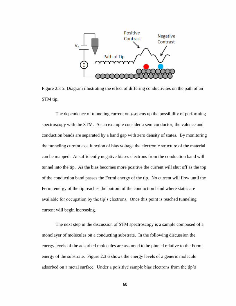
60
Figure 2.3 5: Diagram illustrating the effect of differing conductivites on the path of an
STM tip.
The dependence of tunneling current on opens up the possibility of performing
spectroscopy with the STM. As an example consider a semiconductor; the valence and
conduction bands are separated by a band gap with zero density of states. By monitoring
the tunneling current as a function of bias voltage the electronic structure of the material
can be mapped. At sufficiently negative biases electrons from the conduction band will
tunnel into the tip. As the bias becomes more positive the current will shut off as the top
of the conduction band passes the Fermi energy of the tip. No current will flow until the
Fermi energy of the tip reaches the bottom of the conduction band where states are
available for occupation by the tip‟s electrons. Once this point is reached tunneling
current will begin increasing.
The next step in the discussion of STM spectroscopy is a sample composed of a
monolayer of molecules on a conducting substrate. In the following discussion the
energy levels of the adsorbed molecules are assumed to be pinned relative to the Fermi
energy of the substrate. Figure 2.3 6 shows the energy levels of a generic molecule
adsorbed on a metal surface. Under a poisitive sample bias electrons from the tip‟s
61
conduction band can tunnel into the adsorbed molecule‟s unfilled orbitals and then drain
into the substrate. Electrons from the filled orbitals can not tunnel into the tip because
the conduction band is occupied. A negative sample bias raises the sample and
substrate‟s energy levels allowing electrons from the adsorbate‟s filled orbitals to enter
the tip‟s conduction band. By modulating the bias voltage STM can be used to sudy both
the filled and empty states of an adsorbed molecule.
Figure 2.3 6: Tip-sample energy diagrams with the states of an adsorbed molecule under
a positive sample bias (A) and negative sample bias (B). The arrow indicates the
direction of electron flow.
The clearest way to extract electronic structure data from current vs. voltage data
is to look at the derivative of equation 2.3-8 with respect to voltage which can be
approximated as:128
(2.3-12)
Tunneling current increases with increasing bias voltage because more and more
electrons have enough energy to tunnel into unfilled states. Since tunneling is most
62
probable for electrons near the Fermi level there will be an increase in the tunneling
current as the Fermi level of the tip comes in to resonance with one of the adsorbate‟s
states. As the Fermi energy of the tip moves to higher potentials the tunneling channel
through the adsorbate‟s state does not close, and current still flows through the adsorbate.
Because the tunneling channel does not close off resonance with an adsorbate energy
level is indicated by a change in the slope of the current vs. voltage curve. The density of
states term for the tip contributes a constant factor to dI/dV due to its ohmic character.
The transmission coefficient term increases monotonically with V contributing a rising
background on which the orbital peaks are superimposed.
Having discussed the dependence of tunneling current on density of states we now
turn to a discussion of bias voltage and tip-sample separation. Tunneling increases
linearly with bias voltage and drops off exponentially with tip sample separation. The
choice of bias voltage and tunneling current are important experimental parameters. For
example if the bias voltage is set in the band gap of a semiconductor no current will flow
and the tip will crash. Conversely, if the bias is set in either the valence or conduction
bands electrons will tunnel. The exponential dependence on tunneling current is
particularly germane to STM studies of H2(H4TSPP) nanorods. The nanorods are ~ 4 nm
tall and several may be stacked on top of each other. The risk of crashing the tip into a
rod can be reduced by operating at a low setpoint (1 pA); at the cost of signal strength.
STM experiments can be carried out under ambient conditions or in ultrahigh
vacuum (UHV). Both techniques have their strengths and weaknesses. For example,
ambient STM‟s are capable of atomic resolution, are less expensive to purchase and
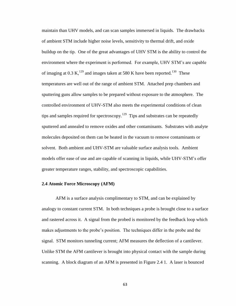
63
maintain than UHV models, and can scan samples immersed in liquids. The drawbacks
of ambient STM include higher noise levels, sensitivity to thermal drift, and oxide
buildup on the tip. One of the great advantages of UHV STM is the ability to control the
environment where the experiment is performed. For example, UHV STM‟s are capable
of imaging at 0.3 K,129
and images taken at 580 K have been reported.130
These
temperatures are well out of the range of ambient STM. Attached prep chambers and
sputtering guns allow samples to be prepared without exposure to the atmosphere. The
controlled environment of UHV-STM also meets the experimental conditions of clean
tips and samples required for spectroscopy.129
Tips and substrates can be repeatedly
sputtered and annealed to remove oxides and other contaminants. Substrates with analyte
molecules deposited on them can be heated in the vacuum to remove contaminants or
solvent. Both ambient and UHV-STM are valuable surface analysis tools. Ambient
models offer ease of use and are capable of scanning in liquids, while UHV-STM‟s offer
greater temperature ranges, stability, and spectroscopic capabilities.
2.4 Atomic Force Microscopy (AFM)
AFM is a surface analysis complimentary to STM, and can be explained by
analogy to constant current STM. In both techniques a probe is brought close to a surface
and rastered across it. A signal from the probed is monitored by the feedback loop which
makes adjustments to the probe‟s position. The techniques differ in the probe and the
signal. STM monitors tunneling current; AFM measures the deflection of a cantilever.
Unlike STM the AFM cantilever is brought into physical contact with the sample during
scanning. A block diagram of an AFM is presented in Figure 2.4 1. A laser is bounced
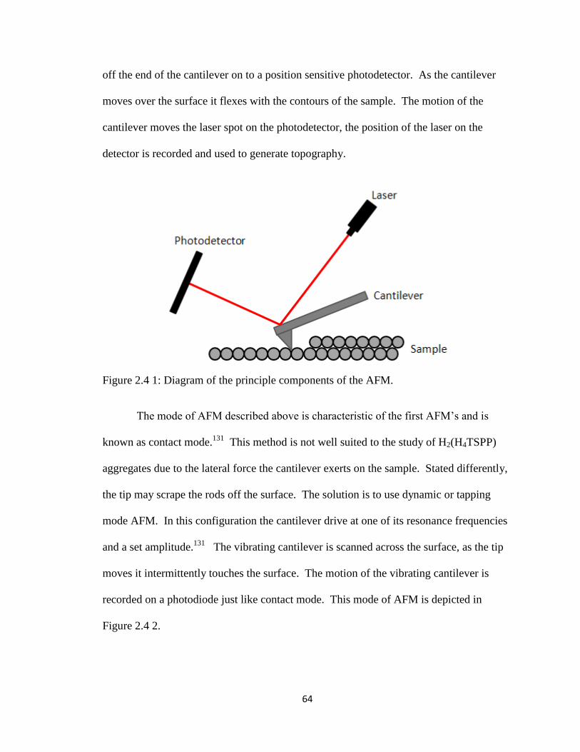
64
off the end of the cantilever on to a position sensitive photodetector. As the cantilever
moves over the surface it flexes with the contours of the sample. The motion of the
cantilever moves the laser spot on the photodetector, the position of the laser on the
detector is recorded and used to generate topography.
Figure 2.4 1: Diagram of the principle components of the AFM.
The mode of AFM described above is characteristic of the first AFM‟s and is
known as contact mode.131
This method is not well suited to the study of H2(H4TSPP)
aggregates due to the lateral force the cantilever exerts on the sample. Stated differently,
the tip may scrape the rods off the surface. The solution is to use dynamic or tapping
mode AFM. In this configuration the cantilever drive at one of its resonance frequencies
and a set amplitude.131
The vibrating cantilever is scanned across the surface, as the tip
moves it intermittently touches the surface. The motion of the vibrating cantilever is
recorded on a photodiode just like contact mode. This mode of AFM is depicted in
Figure 2.4 2.
65
Figure 2.4 2: Diagram depicting tapping mode AFM.
The AFM is a valuable surface analysis tool, because it measures the deflection of
a cantilever it can be used on nonconducting samples ulike STM. The AFM is also better
suited for taking large-scale pictures (10-50 µm) which makes it apropos for optimizing
nanorod deposition. Two types of tapping mode cantilevers were used: Nanosensors
Pointprobe (29-79 N/m spring constant, 290-400 kHz, tip radius of curvature < 10 nm)
and Vistaprobe T300R-25 (20-75 N/m spring constant, 200-400 kHz, tip radius of
curvature < 10 nm)
2.5 Raman Spectroscopy:
Raman spectroscopy uses scattered photons to probe the vibrational character of
molecules. It provides similar information to infrared spectroscopy (IR), but with
different selection rules. The acivity of a vibrational mode in an IR spectrum is based on
the change in a molecule‟s dipole moment as a function of displacement along a normal
66
coordinate. As a consequence homonuclear diatomic molecues such as O2 are inactive in
IR spectroscopy. Raman selection rules are based on the polarizability of a molecule‟s
electron cloud. IR and Raman are complimentary techniques. A vibrational mode which
is active in one technique may or may not be active in the other because of the differing
selection rules.
A two photon process is often used to explain scattering. In the first step a photon
strikes a molecule which is excited to a “virtual state”. From the virtual state the
molecule relaxes to some final state and emits a scattered photon. If the molecule returns
to its initial state (elastic scattering) the emitted photon will have the same wavelength as
the incident photon. This process is the previoulsy discussed RLS and is the most
probable result. If the target molecule relaxes to a vibrationally excited state the scattered
photon will have a wavelegth to the red of the incident photon. The shift in wavelenght
will be equal to the spacing between the intial and final vibrational energy levels. This
case is called Stokes scattering. The final possibility is that an molecule in an excited
vibrational state is excited to the virtual state and decays to the ground vibrational state.
This process is called anti-Stokes scattering, and results in a scattered photon with a blue
shifted wavelength. Anti-Stokes scattering requires a populated excited state, hence it is
the least probable type of scattering as most excited vibrational levels are not significanly
thermally populated.
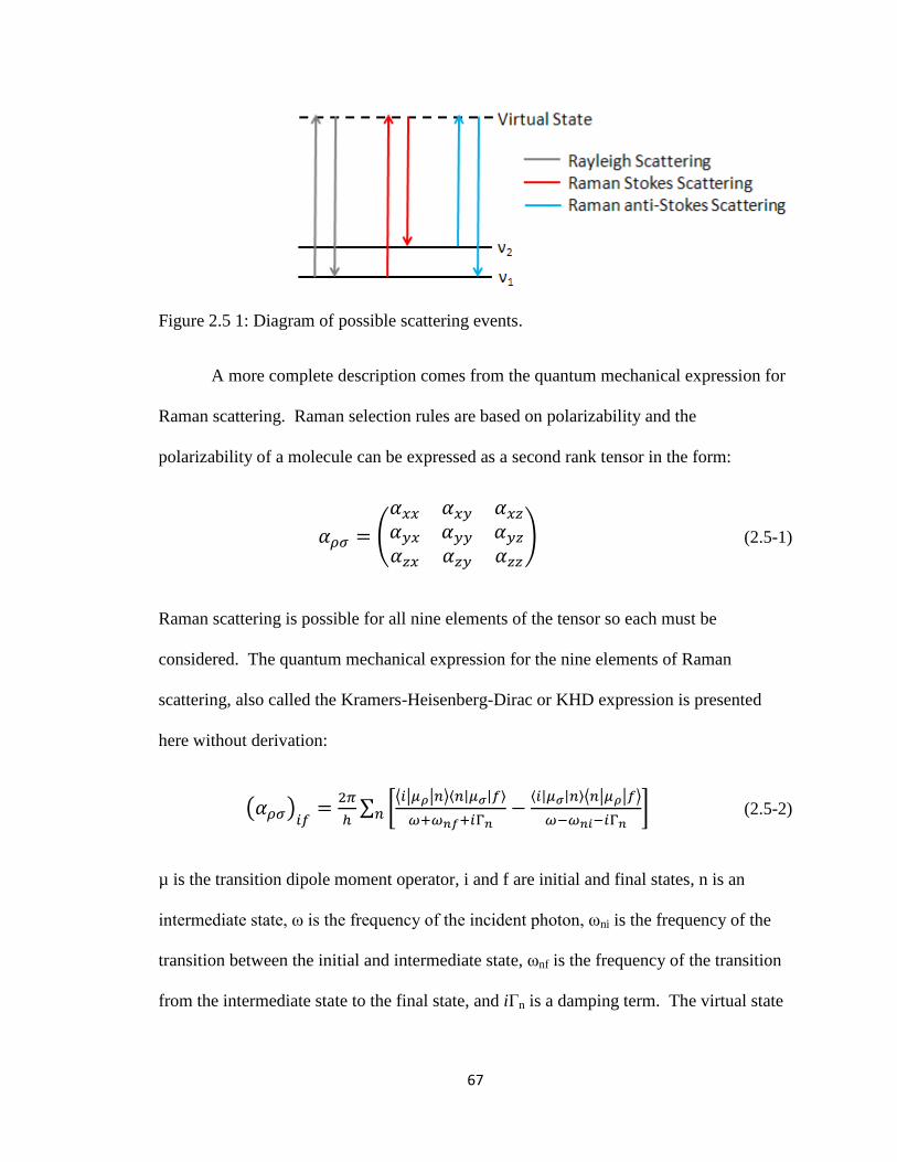
67
Figure 2.5 1: Diagram of possible scattering events.
A more complete description comes from the quantum mechanical expression for
Raman scattering. Raman selection rules are based on polarizability and the
polarizability of a molecule can be expressed as a second rank tensor in the form:
(2.5-1)
Raman scattering is possible for all nine elements of the tensor so each must be
considered. The quantum mechanical expression for the nine elements of Raman
scattering, also called the Kramers-Heisenberg-Dirac or KHD expression is presented
here without derivation:
(2.5-2)
µ is the transition dipole moment operator, i and f are initial and final states, n is an
intermediate state, ω is the frequency of the incident photon, ωni is the frequency of the
transition between the initial and intermediate state, ωnf is the frequency of the transition
from the intermediate state to the final state, and iΓn is a damping term. The virtual state
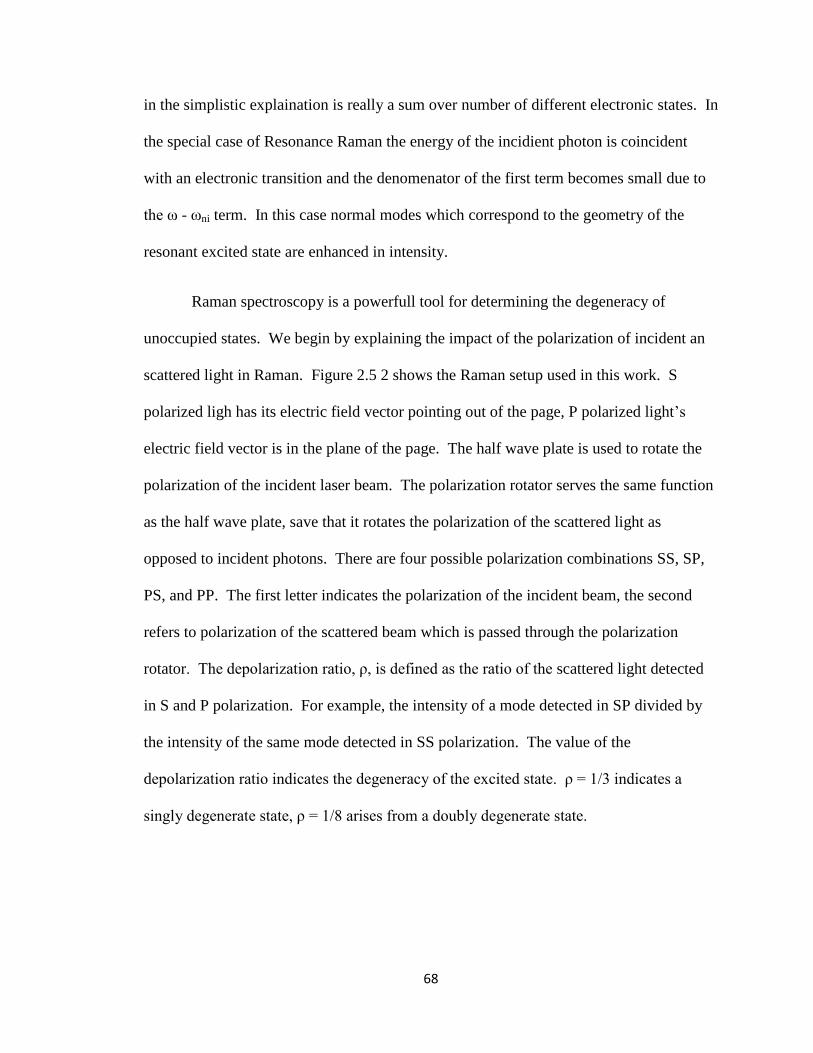
68
in the simplistic explaination is really a sum over number of different electronic states. In
the special case of Resonance Raman the energy of the incidient photon is coincident
with an electronic transition and the denomenator of the first term becomes small due to
the ω - ωni term. In this case normal modes which correspond to the geometry of the
resonant excited state are enhanced in intensity.
Raman spectroscopy is a powerfull tool for determining the degeneracy of
unoccupied states. We begin by explaining the impact of the polarization of incident an
scattered light in Raman. Figure 2.5 2 shows the Raman setup used in this work. S
polarized ligh has its electric field vector pointing out of the page, P polarized light‟s
electric field vector is in the plane of the page. The half wave plate is used to rotate the
polarization of the incident laser beam. The polarization rotator serves the same function
as the half wave plate, save that it rotates the polarization of the scattered light as
opposed to incident photons. There are four possible polarization combinations SS, SP,
PS, and PP. The first letter indicates the polarization of the incident beam, the second
refers to polarization of the scattered beam which is passed through the polarization
rotator. The depolarization ratio, ρ, is defined as the ratio of the scattered light detected
in S and P polarization. For example, the intensity of a mode detected in SP divided by
the intensity of the same mode detected in SS polarization. The value of the
depolarization ratio indicates the degeneracy of the excited state. ρ = 1/3 indicates a
singly degenerate state, ρ = 1/8 arises from a doubly degenerate state.
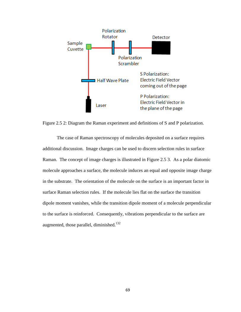
69
Figure 2.5 2: Diagram the Raman experiment and definitions of S and P polarization.
The case of Raman spectroscopy of molecules deposited on a surface requires
additional discussion. Image charges can be used to discern selection rules in surface
Raman. The concept of image charges is illustrated in Figure 2.5 3. As a polar diatomic
molecule approaches a surface, the molecule induces an equal and opposite image charge
in the substrate. The orientation of the molecule on the surface is an important factor in
surface Raman selection rules. If the molecule lies flat on the surface the transition
dipole moment vanishes, while the transition dipole moment of a molecule perpendicular
to the surface is reinforced. Consequently, vibrations perpendicular to the surface are
augmented, those parallel, diminished.132
70
Figure 2.5 3: Diagram of an adsorbed molecule and its image charges. The charges
cancel in the left-hand case and reinforce in the right-hand arrangement.
The concept of augmented and diminished vibrational modes as a consequence of
orientation relative to a surface can be expressed in the following equations (each are
proportional to intensity of the Raman spectra):132
(2.5-3a)
(2.5-3b)
2.5-3c)
(2.5-3d)
The primed quantities correspond to scattered radiation, alphas are the nine components
of the polarizability tensor, r is an optical constant called a Fresnel coefficient, and phi is
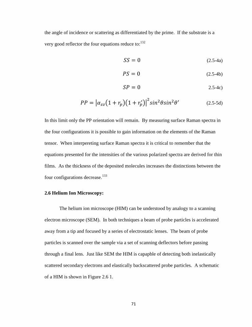
71
the angle of incidence or scattering as differentiated by the prime. If the substrate is a
very good reflector the four equations reduce to:132
(2.5-4a)
(2.5-4b)
2.5-4c)
(2.5-5d)
In this limit only the PP orientation will remain. By measuring surface Raman spectra in
the four configurations it is possible to gain information on the elements of the Raman
tensor. When interpereting surface Raman spectra it is critical to remember that the
equations presented for the intensities of the various polarized spectra are derived for thin
films. As the thickness of the deposited molecules increases the distinctions between the
four configurations decrease.133
2.6 Helium Ion Microscopy:
The helium ion microscope (HIM) can be understood by analogy to a scanning
electron microscope (SEM). In both techniques a beam of probe particles is accelerated
away from a tip and focused by a series of electrostatic lenses. The beam of probe
particles is scanned over the sample via a set of scanning deflectors before passing
through a final lens. Just like SEM the HIM is capapble of detecting both inelastically
scattered secondary electrons and elastically backscattered probe particles. A schematic
of a HIM is shown in Figure 2.6 1.
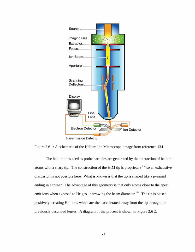
72
Figure 2.6 1: A schematic of the Helium Ion Microscope. image from reference 134
The helium ions used as probe particles are generated by the interaction of helium
atoms with a sharp tip. The construction of the HIM tip is proprietary134
so an exhaustive
discussion is not possible here. What is known is that the tip is shaped like a pyramid
ending in a trimer. The advantage of this geometry is that only atoms close to the apex
emit ions when exposed to He gas, narrowing the beam diameter.134
The tip is biased
positively, creating He+ ions which are then accelerated away from the tip through the
previously described lenses. A diagram of the process is shown in Figure 2.6 2.
73
Figure 2.6 2: A schematic of the Helium Ion Microscope Tip. image from reference 134
The HIM has a few advantages over the SEM. First, the secondary electron yield
per particle is two to eight times higher in HIM than SEM. Higher secondary electron
yield means better signal strength and clearer pictures. Second, the the use of an electron
flood gun in tandem with the He+ beam eliminates charging so nonconducting samples
can be imaged without sputtering and consequent loss of detail.135
Third, the smaller
DeBroglie wavelength of helium allows for better resolution. As of 2010 the ORION®
PLUS manufactured by Carl Zeiss has better resolution (0.24 nm136
) than the best SEM
on the market; the Hitachi S-5500 (0.4 nm137
). Fourth, the energy of the inelastically
scattered secondary electrons is much lower in HIM than SEM allowing for more surface
detail in images.138
2.7 Transmission Electron Microscopy:
Transmission Electron Microscopy (TEM) is a microscopy technique based upon
the scattering of electrons by atoms in a sample. For this discussion we will consider thin
samples (defined as <20 nm139
). Electrons are generated in a gun by Schottky,
thermionic, or field emission. The gun is held at a negative potiential which accelerates
74
the electrons away from the gun and through a series of electronic lenses which focus the
beam onto the sample. Acceleration voltages vary, ranging from 200-500 kV to as high
as 3 MV for high resolution work.140
Image contrast is created by the scattering of
electrons by the sample (this is called scattering contrast). For this discussion we will
limit ourselves to bright field imaging which detects electrons passing through the
specimen unscattered. Electron scattering by atoms in the sample can be described in
detail by Coulombic interactions, for the purposes of this discussion a much simpler
model will suffice. The loss of electrons by scattering events (T) can be described by the
following empirical equation:139
(2.7-1)
Where Z is atomic number, A is the atomic weight , b and a are empirical constants, and
x is the mass thickness defined as the sample density multiplied by the thickness of the
sample. This equation illustrates several important aspects of TEM. Heavier atoms (high
Z and A) will scatter more than low Z materials leading to better scattering contrast.
Second, thicker samples will scatter more than thinner samples. Third, the electron loss
due to scattering is logarithmic, so thin samples are required. After interaction with the
sample the unscattered electrions are imaged by a photographic plate or a CCD camera
attached to a fluorescent screen.140
TEM is capable of resolution superior to both SEM
and HIM. The FEI Titan G2 60-300 TEM has a resolution of 80 pm.141

75
Chapter 3: Experimental Methods
3.1 Materials, Reagent, and Instrument List
The following reagents and materials were used in course of this project:
Reagent grade concentrated hydrochloric acid
Reagent grade concentrated nitric acid
Reagent grade 30% hydrogen peroxide (stabilized)
Reagent grade sodium hydroxide pellets
α,β,γ,δ-tetrasulfonatophenylporphine dihydrochloride (Frontier Scientific T1239)
http://www.frontiersci.com/
Tetrasodium α,β,γ,δ-tetrasulfonatophenylporphine dodecahydrate (Alfa Aesar 30538)
http://www.alfa.com/
Chloroauric acid trihydrate (HAuCl4•3H2O Aldrich 520918-G)
http://www.sigmaaldrich.com/sigma-aldrich/home.html
99.999% pure gold splatters (Cerac G-1065) http://www.cerac.com/
1x4 cm mica sheets (Ted Pella #54) http://www.tedpella.com/
9.9 cm diameter mica disks (Ted Pella #50) http://www.tedpella.com/
GridStick TM
adhesive (Ted Pella #155-9) http://www.tedpella.com/
76
Highly ordered pyrolytic graphite 5x5x1, 7x7x1, 10x10x1 mm SPI-2 grade (SPI supplies
479HP-AB, 480HP-AB, 436HP-AB) http://www.2spi.com/
Tungsten wire 0.25 mm diameter 99.95% pure (Alfa Aesar 10408) http://www.alfa.com/
Platinum0.8Iridum0.2 wire 0.25 mm diameter (California Fine Wire Company 100168)
http://www.calfinewire.com/
AFM tapping mode cantilevers 29-79 N/m 290-400 kHz (Nanosensors Pointprobe)
http://www.nanosensors.com/
AFM tapping mode cantilevers 20-75 N/m 200-400 kHz (Vistaprobe T300R-25)
http://www.vistaprobes.com/vp/
UV-visible cuvettes 1cm path length 170-2200 nm range (Spectrocell R-3010-T)
http://www.spectrocell.com/Spectrocel-old/index.htm
Fluorescence cell 1 cm path length (Precision Cells Inc. 3G10)
http://www.precisioncells.com/
The following instruments were used in the course of this project:
Ultraviolet-Visible Absorption Spectroscopy:
Perkin-Elmer 330 UV-visible spectrophotometer (www.perkinelmer.com)
Shimadzu UV-2501PC UV-visible spectrophotometer (www.shimadzu.com)
Resonance Light Scattering Spectroscopy:

77
PTI Quanta Master Fluorimeter (www.pti-nj.com)
Raman Spectroscopy:
Spex 14018 Spectrometer outfitted with a double monochromator and thermoelectrically
cooled photomultiplier tube detection.
Lexel Model 95 Ar ion laser (www.lexellaser.com)
Spectra Physics Beamlock 2060 Kr ion laser (www.newport.com)
Atomic Force Microscopy:
Digital Instruments Nanoscope II AFM (www.veeco.com)
Molecular Imaging Pico Plus combination AFM/STM (www.agilent.com)
Ambient Scanning Tunneling Microscopy:
Molecular Imaging Pico 5 STM (Equipped with a 1 µm STM head) (www.agilent.com)
Molecular Imaging Pico Plus combination AFM/STM (Equipped with a 1 µm STM head
with a low current preamp) (www.agilent.com)
Ultra-High Vacuum Scanning Tunneling Microscopy:
Model UHV300 Scanning Tunneling Microscope and control electronics (model
SPM100) from RHK Technology (www.RHK-tech.com)
Helium Ion Microscopy:
Carl Zeiss ORION® PLUS Helium Ion Microscope (www.zeiss.com)
78
Transmission Electron Microscopy:
Philips CM-200 Transmission Electron Microscope (www.fei.com)
Scanning Electron Microscopy:
FEI 200F Scanning Electron Microscope (www.fei.com)
X-ray and Ultraviolet Photoelectron Spectroscopy:
Kratos Axis-165 electron spectrometer (www.kratos.com)
3.2 Glassware Cleaning Procedure
In order to keep aggregation conditions constant all glassware was cleaned with a
solution of 20 parts concentrated nitric acid, 2 parts 30% hydrogen peroxide, and 5 parts
deionized water. The corrosive and oxidizing properties of the solution ensured
consistently clean glass surfaces during aggregation. The cleaning solution was prepared
in either a large beaker or crystallization dish with space left to prevent boil-over. If a
beaker is to be used it is advisable to set the beaker with cleaning solution in a larger
beaker to serve as double containment. The beaker or crystallization dish was covered
with a watch glass during cleaning. The glassware was soaked in the cleaning solution
for at least 2 hours. After soaking, the cleaning solution was stored in a container for
reuse up to three times. The cleaned glassware was rinsed 10 times in deionized water
and allowed to dry. If desired the cleaning solution can be boiled to shorten soaking time
to 1 hour, we elected not to do this due to the risk of severe bumping.
79
3.3 Preparation of Au(111)/mica Substrates
Au(111)/mica substrates were made by vapor depositing 99.999% pure gold
splatters on mica in a UHV chamber. Mica slides were repeatedly cleaved with clear tape
or a razor blade, cut into pieces, and placed in a mask positioned over a tungsten boat
filled with ~ 1 g of gold splatters. The chamber was pumped down to 500 mTorr and
then cleaned by glow discharge with nitrogen plasma five times. After evacuation of the
chamber with a cryo pump the mica was outgassed by heating at ~ 500°C for several
hours via a heater inside a copper block. While the mica outgassed the tungsten boat
with the gold splatter was outgassed by repeatedly heating to ~ 500°C for a period of one
hour. Just prior to deposition the mica was cooled to 350°C and held there for the
duration of the deposition. Deposition of the gold was carried out by resistively heating
the tungsten boat until the Au began to sublime. The deposition rate was monitored by a
quartz film thickness monitor until the rate stabilized. After stabilization the mica
substrates were rotated over the gold boat and held there until the desired thickness was
achieved. The rate of deposition was monitored periodically during deposition with a
quartz film thickness monitor. Thicknesses were typically in the range of 1000 to 2000
Å, with deposition rates ranged from 0.1 Å/s to 1 Å/s. The chamber pressure during
deposition was kept below 4x10⁻⁹
Torr. After deposition the copper block and gold boat
were allowed to cool to room temperature before the chamber was opened and the new
Au(111)/mica samples removed. The cooling procedure took several hours.
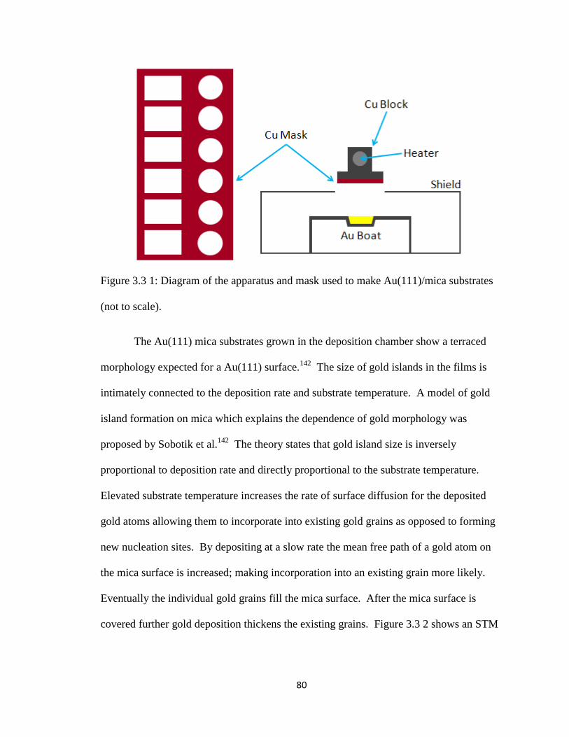
80
Figure 3.3 1: Diagram of the apparatus and mask used to make Au(111)/mica substrates
(not to scale).
The Au(111) mica substrates grown in the deposition chamber show a terraced
morphology expected for a Au(111) surface.142
The size of gold islands in the films is
intimately connected to the deposition rate and substrate temperature. A model of gold
island formation on mica which explains the dependence of gold morphology was
proposed by Sobotik et al.142
The theory states that gold island size is inversely
proportional to deposition rate and directly proportional to the substrate temperature.
Elevated substrate temperature increases the rate of surface diffusion for the deposited
gold atoms allowing them to incorporate into existing gold grains as opposed to forming
new nucleation sites. By depositing at a slow rate the mean free path of a gold atom on
the mica surface is increased; making incorporation into an existing grain more likely.
Eventually the individual gold grains fill the mica surface. After the mica surface is
covered further gold deposition thickens the existing grains. Figure 3.3 2 shows an STM
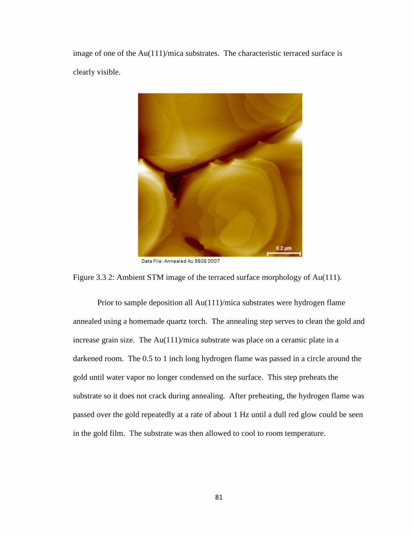
81
image of one of the Au(111)/mica substrates. The characteristic terraced surface is
clearly visible.
Figure 3.3 2: Ambient STM image of the terraced surface morphology of Au(111).
Prior to sample deposition all Au(111)/mica substrates were hydrogen flame
annealed using a homemade quartz torch. The annealing step serves to clean the gold and
increase grain size. The Au(111)/mica substrate was place on a ceramic plate in a
darkened room. The 0.5 to 1 inch long hydrogen flame was passed in a circle around the
gold until water vapor no longer condensed on the surface. This step preheats the
substrate so it does not crack during annealing. After preheating, the hydrogen flame was
passed over the gold repeatedly at a rate of about 1 Hz until a dull red glow could be seen
in the gold film. The substrate was then allowed to cool to room temperature.
82
Au(111)/mica substrates were used to check the condition of STM tips when
imaging in vacuum. The Au(111)/mica substrates were hydrogen-flame annealed, loaded
into the RHK, and heated to 400°C for 3 min to drive off volatile contaminants. After the
initial heating the gold was Ar+ sputtered for 3 min and reannealed at 300°C for 3 min.
This process was repeated (usually 2-3 times) until a clean surface with repeatable
current vs. voltage curves was achieved.
The preparation of HOPG substrates for microscopy was much simpler than
Au(111)/mica. The HOPG was repeatedly cleaved with clear tape to expose a clean
surface prior to deposition. No further preparation was used.
3.4 Preparation of STM Tips
STM tips were prepared from 0.25 mm diameter Pt0.8Ir0.2 and 0.25 mm W wire.
Pt0.8Ir0.2 tips were prepared by either cutting with sharp scissors or electrochemical
etching. The Pt0.8Ir0.2 wire was etched in 2 M NaCl with a Ni ribbon as the counter
electrode. The wire was cleaned prior to etching by immersing it halfway in the
electrolyte and applying a bias of 7 V for ~5 sec. After cleaning the wire was lowered
until it touched the surface of the electrolyte and advanced 0.5 mm into the electrolyte
solution. The main etch was carried out at 25 V until etching ceased. A post etch
cleaning was performed by the same procedure as the pre etch cleaning. The tip was
sequentially dipped in three beakers of Millipore water. The tip was dried by touching a
Kimwipe to the shaft of the tip removing water drops by capillary action. Care was taken
to keep the Kimwipe away from the apex of the tip. The tips were examined under a
83
microscope to ensure sharpness. Pt0.8Ir0.2 tips were used in both UHV and ambient STM
experiments.
Electrochemically etched W tips were used exclusively for UHV-STM. Prior to
etching the W wire was annealed in a high vacuum bell jar at 10-6
torr. Three segments
of W wire 8” long were placed in the bell jar and annealed by passing 6.7 A of current
through a wire for 30 min. Each wire was annealed separately. After annealing, the tips
were etched in 1 M NaOH with graphite as the counter electrode. The wire was cleaned
prior to etching by lowering halfway in the electrolyte and applying a bias of 5 V for ~5
sec. After cleaning 5 mm of the wire was immersed in the electrolyte solution and etched
at 5 V until etching ceased. A post etch cleaning was performed by the same procedure
as the pre etch cleaning. The tip was dipped in three beakers of Millipore water
sequentially and dried with a Kimwipe. The tips were examined under a microscope and
discarded if unsatisfactory. The tips were deemed unsatisfactory if dull, split, or
otherwise macroscopically misshapen.
When used for UHV-STM both types of tips were cleaned by Ar+ sputtering and
checked on a Au(111)/mica sample which was cleaned by repeated cycles of Ar+
sputtering and annealing. The tips were evaluated for resolution by examining the
Au(111) reconstruction. Current Voltage (I(V)) curves were run on the Au(111) to
ensure linearity. Figure 3.4 1 shows the Au(111) reconstruction and an I(V) curve.
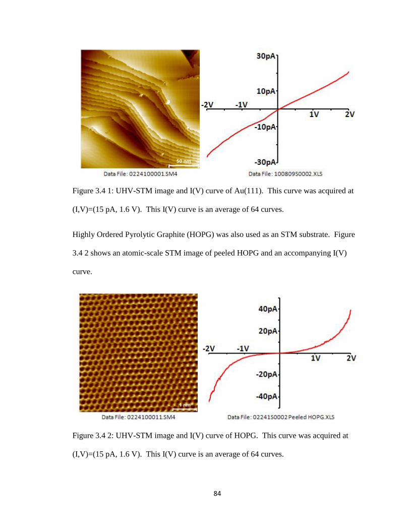
84
Figure 3.4 1: UHV-STM image and I(V) curve of Au(111). This curve was acquired at
(I,V)=(15 pA, 1.6 V). This I(V) curve is an average of 64 curves.
Highly Ordered Pyrolytic Graphite (HOPG) was also used as an STM substrate. Figure
3.4 2 shows an atomic-scale STM image of peeled HOPG and an accompanying I(V)
curve.
Figure 3.4 2: UHV-STM image and I(V) curve of HOPG. This curve was acquired at
(I,V)=(15 pA, 1.6 V). This I(V) curve is an average of 64 curves.
85
3.5 Preparation of Unaggregated and Aggregated Porphyrin Solutions
Both the sodium salt (Na4(H2TSPP)) and the chloride salt (H4(H4TSPP)Cl2) of
tetrasulfonatophenylporphine were used in this study. The H2(H4TSPP) nanorods made
from the different starting materials were indistinguishable save for the presence of
sodium ions when the sodium salt was employed. Free base solutions were made by
dissolving Na4(H2TSPP) in Millipore water previously degassed by boiling for 1 hr to
make a 1-5 mM solution which was then diluted to make solutions ranging from 1 to 50
µM. The pH was adjusted with NaOH over a range of 7.65 to 12.84. Solutions of the
unaggregated diacid were prepared by dissolving H4(H4TSPP)Cl2 in sufficient Millipore
water (also degassed by boiling) to make a 1-5 mM solution which was then diluted to
make solutions ranging from 1 to 50 µM. Diacid solution pH was adjusted with HCl and
ranged from 2 to 3.7. Solution concentrations were checked via the intensity of the Soret
band in UV-visible spectra. The extinction coefficients are ε413 nm = 533000 M-1
cm-151
(free base) and ε434 nm = 443000 M-1
cm-1143
(diacid).
The H2(H4TSPP) aggregates were synthesized by methods previously
reported.66,105,144-146
The porphyrin salt was diluted in Millipore water previously
degassed by boiling for 1 hour to make a 1-5 mM stock solution. The stock solution was
further diluted to the micromolar range and then combined with an equal volume of HCl
to initiate aggregation. The aggregate solution used for most SPM experiments was 5 µM
H2(H4TSPP) in 0.75 M HCl. Solutions of 50 µM H2(H4TSPP) in 0.75 M HCl were used
in Raman experiments.
86
3.6 Preparation of H2(H4TSPP) Nanorod Solutions Containing Chloroauric Acid
To investigate the effects of gold ions on aggregate formation and morphology
several samples were prepared with concentrations of HAuCl4 ranging from 0.1 to 5 µM.
Two protocols were used to prepare the gold/nanorod solutions. The first protocol
involved adding chloroauric acid to the acid solution prior to mixing it with an equal
volume of porphyrin. In the second protocol a few microliters of concentrated
chloroauric acid was added to the already aggregated nanorod sample. Small aliquots
were use to keep changes in solution volume small.
3.7 Preparation and Analysis of STM and AFM Samples
3.7.1 SPM Sample Preparation
SPM samples were prepared using freshly made solutions of TSPP having
molarity in the range of 1 μM to 10 μM. HCl concentrations ranged from 0.3 M to 1.5
M. HOPG and Au(111)/mica were used as substrates. The HOPG substrates were
repeatedly cleaved with clear plastic tape prior to deposition. The Au(111)/mica
substrates were H2 flame annealed prior to deposition.
SPM samples were made using two different protocols. The first protocol
involved placing a drop of solution on the substrate followed by spin drying for 30
seconds at 4000 rpm. Deposition times ranged from 20 min to 2 hrs. During deposition
the substrates were affixed to an AFM puck by double-sided tape. The puck was affixed
to the spin chuck by double-sided tape as well. This setup is illustrated in Figure 3.7.1 1.
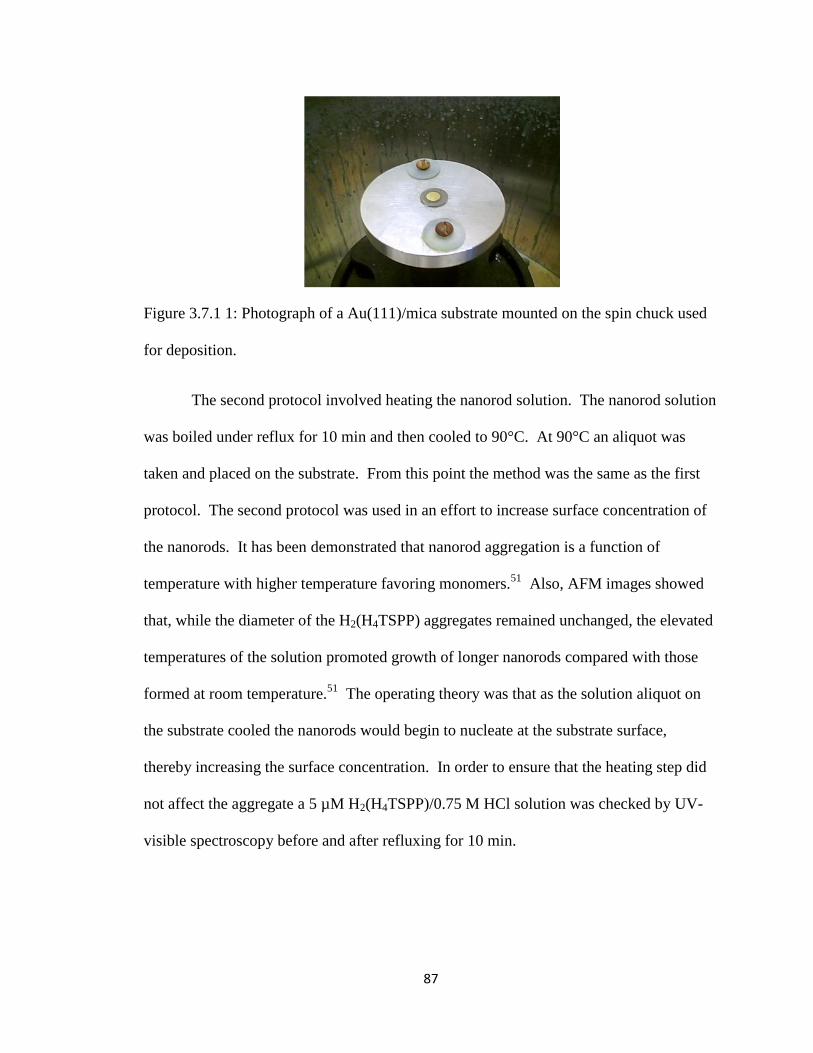
87
Figure 3.7.1 1: Photograph of a Au(111)/mica substrate mounted on the spin chuck used
for deposition.
The second protocol involved heating the nanorod solution. The nanorod solution
was boiled under reflux for 10 min and then cooled to 90°C. At 90°C an aliquot was
taken and placed on the substrate. From this point the method was the same as the first
protocol. The second protocol was used in an effort to increase surface concentration of
the nanorods. It has been demonstrated that nanorod aggregation is a function of
temperature with higher temperature favoring monomers.51
Also, AFM images showed
that, while the diameter of the H2(H4TSPP) aggregates remained unchanged, the elevated
temperatures of the solution promoted growth of longer nanorods compared with those
formed at room temperature.51
The operating theory was that as the solution aliquot on
the substrate cooled the nanorods would begin to nucleate at the substrate surface,
thereby increasing the surface concentration. In order to ensure that the heating step did
not affect the aggregate a 5 µM H2(H4TSPP)/0.75 M HCl solution was checked by UV-
visible spectroscopy before and after refluxing for 10 min.
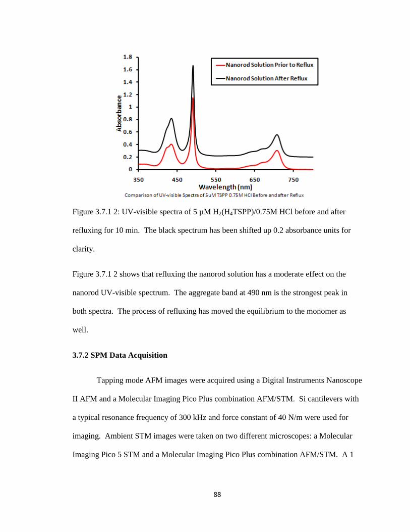
88
Figure 3.7.1 2: UV-visible spectra of 5 µM H2(H4TSPP)/0.75M HCl before and after
refluxing for 10 min. The black spectrum has been shifted up 0.2 absorbance units for
clarity.
Figure 3.7.1 2 shows that refluxing the nanorod solution has a moderate effect on the
nanorod UV-visible spectrum. The aggregate band at 490 nm is the strongest peak in
both spectra. The process of refluxing has moved the equilibrium to the monomer as
well.
3.7.2 SPM Data Acquisition
Tapping mode AFM images were acquired using a Digital Instruments Nanoscope
II AFM and a Molecular Imaging Pico Plus combination AFM/STM. Si cantilevers with
a typical resonance frequency of 300 kHz and force constant of 40 N/m were used for
imaging. Ambient STM images were taken on two different microscopes: a Molecular
Imaging Pico 5 STM and a Molecular Imaging Pico Plus combination AFM/STM. A 1
89
µm STM head with a low tunneling current preamp (0.1 nA/V) was used for ambient
STM on the Pico Plus.
Samples for UHV-STM analysis were transferred via air-lock into the STM
vacuum chamber (working pressure < 1x10⁻¹⁰
Torr) where the aggregate samples were
heated to 100C for a period of 2 min in order to remove HCl and water. Non-aggregated
samples were heated to temperatures between 100 and 200C prior to image collection.
The STM and controller were purchased from RHK technology and both constant current
images and I(V) data were acquired with this system. Unless otherwise stated, the
images were plane-fit and low-pass filtered. Most of the data was acquired at either at
293K or 90K on HOPG, but a few images and I(V) curves were obtained from nanorods
on Au(111). Both etched W and Pt0.8Ir0.2 tips were used. Generally, the tips required a
cleaning step (Argon ion sputtering) in order to produce high quality I(V) curves on a
clean gold surface. Spectroscopy was performed by using the RHK software to measure
current as a function of sample bias voltage, I(V), at fixed tip-sample separation
(feedback off). Multiple curves were acquired at each setting and then averaged. dI/dV
curves were obtained as a numerical derivative of the average I(V). Orbital mediated
tunneling spectra, OMTS, (dI/dV at fixed height) were measured on well defined
monolayer islands of the porphyrin on HOPG. While dI/dV was determined on nanorod
structures (and is reported here), it should not be interpreted as OMTS since the primary
conduction mechanism of the nanorods in positive bias is not tunneling. Rather, dI/dV is
simply related only to the conductivity of the nanorods.
90
3.8 Preparation of Raman Samples
Solution Raman and surface Raman spectra of the various porphyrin solutions and
gold-adsorbed porphyrin samples, respectively, were acquired with a Spex 14018
Spectrometer outfitted with a double monochromator and thermoelectrically cooled
photomultiplier tube detection. Solution phase spectra were obtained at a 90° scattering
geometry using a quartz flow cell. The analyte was pumped through the flow cell via a
peristaltic pump to avoid sample degradation. Absorption spectra were recorded before
and after acquisition of the Raman spectrum to confirm sample integrity. Raman spectra
were excited with vertically polarized light. The vertical (polarized) and horizontal
(depolarized) components of the scattered light were detected by means of a polarization
analyzer, followed by a scrambler to eliminate the polarization bias of the
monochromator/detector. Three different laser wavelengths were used for excitation: 488
nm and 457.9 nm lines of the Ar ion laser were used for the aggregate and diacid
respectively. The 413.1 nm line of a Kr ion laser was used to excite the spectrum of the
free base. Laser powers ranged from 15 to 60 mW for solution samples. The displayed
data were collected with a 2 cm-1
integration interval.
50 μM porphyrin solutions of the free base and unaggregated diacid were used to
acquire monomeric solution Raman spectra. 5 and 50 µM H2(H4TSPP) solutions were
used to acquire the solution Raman spectrum of the aggregate. Surface substrates were
prepared by vapor depositing gold on pre-cleaned glass microscope slides and mica
substrates. The gold on glass films were deposited a rate 0.2 nm/s in a high-vacuum
deposition chamber at a base pressure of 5 × 10⁻⁷
Torr. The gold on mica films were
91
deposited in the same fashion as the Au(111)/mica substrates used for SPM studies. For
the sample adsorbed on Au(111), Raman spectra were excited with both vertically and
horizontally polarized light by using a half-wave plate to rotate the polarization of the
incident light, followed by detection of both the vertical and the horizontal components of
the scattered light to generate SS, SP, PS, and PP spectra. Aggregate samples on
Au(111) were prepared by deposition from a 5 μM solution of H2(H4TSPP) in 0.75 M
HCl when using 488 nm excitation and from a 50 μM solution in 0.75 M HCl for
measurements at the 413 nm line. Raman samples were prepared by placing a drop of the
5 μM porphyrin solution on Au(111) substrate (same as for the STM samples) for 1 h
followed by spinning for 30 s at 4000 rpm. Higher porphyrin concentration for surface
Raman samples were made by allowing a drop of the 50 μM solution to completely
evaporate from the Au(111) surface. The gold substrates were mounted in a spinner
rotating at 3000 rpm oriented such that the angle between the propagation direction and
the surface normal was fixed at 66 and 24° for the incident and scattered beams,
respectively.
3.9 Preparation of UV-visible and Resonance Light Scattering Samples
Electronic absorption spectra of the porphyrin in solution and as thin solid films
along with appropriate references were collected with Perkin-Elmer 330 and a Shimadzu
UV-2501PC UV-visible spectrophotometers. Quartz cuvettes of 1 mm and 10 mm were
used for the solution spectra measurements of monomer, free base, and aggregated
porphyrin. Porphyrin concentrations for UV-visible studies ranged from 1 μM to 50 μM.
The pH was adjusted with either NaOH or HCl. For liquid phase spectral measurements,
92
we employed aqueous reference solutions of the same pH as the sample. Pre-cleaned 3
mm thick and 3 cm in diameter quartz disks were employed for depositing a thin film of
H2(H4TSPP) aggregate from solution. H2(H4TSPP) solid samples were prepared by
placing 0.1 mL of the aggregate solution on a quartz plate for 90 min followed by spin-
drying at 4000 rpm for 30 s. A matching quartz disk was treated with an acidified
solution containing no porphyrin and served as a reference. RLS spectra were measured
with a PTI Quanta Master Fluorimeter using a 1.00 cm quartz fluorescence cell and slit
widths of 0.125 and 2.00 nm for excitation and emission, respectively. RLS intensities
were recorded by scanning simultaneously the excitation and emission monochromators
(Δλ = 10 nm) from 200 to 800 nm. A porphyrin concentration range of 0.74 to 5.9 μM in
0.75 M HCl was used.
3.10 Preparation and Measurement of XPS and UPS Samples
3.10.1 UPS and XPS Sample Preparation
XPS and UPS samples were prepared by two different methods. Powder XPS
samples were pressed into In shot. Aggregate UPS and XPS samples were prepared by
depositing 5 µM H2(H4TSPP) in 0.75 M HCl on either Au(111) or HOPG substrates
followed by spin drying at 4000 rpm for 30 seconds. The aggregate was deposited on
Au(111) for 90 min and on HOPG for 60 min. The monomer was deposited on HOPG
for 40 min.
3.10.2 UPS Spectral Acquisition
93
UPS data were obtained with a homemade He lamp source and the He I (21.2 eV)
line was used exclusively. A platinum coated concave 600 groove/mm reflection grating
with a 3.5 blaze angle coupled with a gold coated spherical focusing mirror was used to
produce monochromatic UV radiation. The base pressure in the monochromator chamber
was 8x10⁻¹⁰
Torr. The UPS system is attached via a UHV valve to a Kratos Axis-165
electron spectrometer having a base pressure of 8x10⁻¹⁰
Torr.
First, the appropriate reference surfaces were studied. These HOPG and Au(111)
samples were then used as substrates for the porphyrin structures prepared as described
above. Samples were heated to 100°C in UHV prior to final measurement. The UPS
data was acquired using a hybrid lens that focused the ejected electrons into the Kratos
spectrometer. A bias of – 20 V was applied to the sample to shift the spectra out of the
non-linear region of the analyzer (KE = 0-10 eV). The spectrometer was used in fixed
analyzer transmission mode with a pass energy of 10 eV and spatial resolution of 120
µm. The photo-emitted electron energies were analyzed by a Kratos hemispherical
analyzer and counted by 8 channel electron multipliers. Under these conditions the
energy resolution of the spectrometer is better than 150 meV which was determined at the
Fermi edge of an Ar etched silver sample.
3.10.3 XPS Spectral Acquisition
Porphyrin samples for XPS analysis were prepared with the same procedures as
for the UPS samples. 180-200 watts of achromatic radiation at energy 1253.6 eV (MgKα)
was used as XPS excitation sources. The analyzer was set for a spatial resolution of 120
µm. The energy resolution was set to 1.0 eV for survey spectra, and to 0.15 eV for the
94
higher resolution acquisitions of C 1s, N1s, S 2p, and Au 4f7/2 peaks. Binding energies
were calibrated against the Au 4f7/2 peak taken to be located at BE = 84.3 eV and against
the C1s peaks for HOPG samples (BE=284.5 eV).
3.11 Preparation of Helium Microscope Samples
Samples to be analyzed by Helium Ion Microscopy (HIM) were prepared using
freshly made solutions of 5 μM H2(H4TSPP) in 0.75 M HCl. HOPG and Au(111)/mica
were used as substrates. HOPG substrates were repeatedly cleaved with clear plastic tape
prior to deposition. The Au(111)/mica substrates were H2 flame annealed prior to
deposition.
HIM samples were made by placing a drop of solution on the substrate followed
by spin drying for 30 seconds at 4000 rpm. Each sample was deposited for 1 hr. During
deposition the substrates were affixed to an AFM puck by double-sided tape. The puck
was affixed to the spin chuck by double-sided tape as well. This setup is illustrated in
Figure 3.7.1 1. HIM samples were checked by AFM prior to imaging by HIM. The
microscope used was an ORION® PLUS manufactured by Carl Zeiss located at Pacific
Northwest National Lab in Richland, Wa.
3.12 Preparation of Transmission Electron Microscopy Samples
TEM samples were made by placing a drop of solution on a carbon coated Ni
Formvar TEM grid attached to an AFM puck with GridStick TM
adhesive. The AFM
puck was affixed to the spin chuck with double sided tape. After a 20-40 min deposition
95
the substrate was spun dry for 30 seconds at 4000 rpm. The samples were analyzed on a
Phillips CM-200 TEM.
3.13 Optimization of H2(H4TSPP) geometry with Electron Affinity and Ionization
Potential Calculation.
All calculations were performed using the commercial program Gaussian03. All
reported results are based on Density Functional Theory (DFT) calculations using the
B3LYP functional and the 6-31+G(d,p) basis, or the 6-31+G(2d,p) basis in the case of
Nickel Tetraphenylporphyrin (NiTPP). Ionization potentials and electron affinities were
determined by computing the energy differences between initial molecule and the
appropriate ionized species, usually in the computed equilibrium geometry of the gas
phase parent molecule (vertical IP and EA). In a few cases, the geometry of the ionized
species was also optimized. Solution phase IP and EA values were determined using the
PCM method with the Gaussian03 parameters for acetonitrile.
3.14 Fabrication of and Current vs. Voltage Measurements of H2(H4TSPP)
Nanorods Deposited on Interdigitated Electrodes
Interdigitated electrodes (IdE‟s) were fabricated by the University of California
Santa Barbara Nanofabrication Facility (http://www.nanotech.ucsb.edu/). The electrodes
were modeled after a design previously reported.49
A 400 nm oxide layer was grown on
a p doped silicon wafer. Interdigitated Au electrodes were deposited via
photolithography on a chromium adhesion layer. A schematic of the device is presented
in Figure 3.14 1.
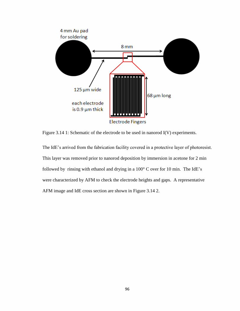
96
Figure 3.14 1: Schematic of the electrode to be used in nanorod I(V) experiments.
The IdE‟s arrived from the fabrication facility covered in a protective layer of photoresist.
This layer was removed prior to nanorod deposition by immersion in acetone for 2 min
followed by rinsing with ethanol and drying in a 100° C over for 10 min. The IdE‟s
were characterized by AFM to check the electrode heights and gaps. A representative
AFM image and IdE cross section are shown in Figure 3.14 2.
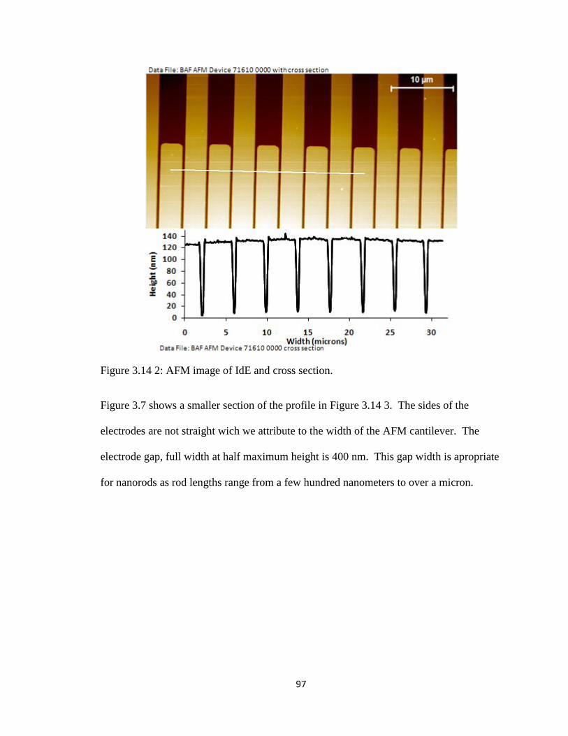
97
Figure 3.14 2: AFM image of IdE and cross section.
Figure 3.7 shows a smaller section of the profile in Figure 3.14 3. The sides of the
electrodes are not straight wich we attribute to the width of the AFM cantilever. The
electrode gap, full width at half maximum height is 400 nm. This gap width is apropriate
for nanorods as rod lengths range from a few hundred nanometers to over a micron.
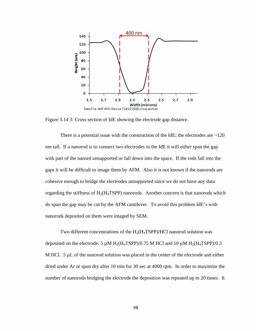
98
Figure 3.14 3: Cross section of IdE showing the electrode gap distance.
There is a potential issue with the construction of the IdE; the electrodes are ~120
nm tall. If a nanorod is to connect two electrodes in the IdE it will either span the gap
with part of the nanord unsupported or fall down into the space. If the rods fall into the
gaps it will be difficult to image them by AFM. Also it is not known if the nanorods are
cohesive enough to bridge the electrodes unsupported since we do not have any data
regarding the stiffness of H2(H4TSPP) nanorods. Another concern is that nanorods which
do span the gap may be cut by the AFM cantilever. To avoid this problem IdE‟s with
nanorods deposited on them were imaged by SEM.
Two different concentrations of the H2(H4TSPP)/HCl nanorod solution was
deposited on the electrode: 5 µM H2(H4TSPP)/0.75 M HCl and 10 µM H2(H4TSPP)/0.3
M HCl. 5 µL of the nanorod solution was placed in the center of the electrode and either
dried under Ar or spun dry after 10 min for 30 sec at 4000 rpm. In order to maximize the
number of nanorods bridging the electrode the deposition was repeated up to 20 times. It
99
has been reported in the literature that H2(H4TSPP) nanorods are photoconducting.49
In
order to control this variable the IdE was affixed to the bottom of an electronics box with
double sided tape. Leads connected to BNC‟s grounded to the box were soldered onto
the Au pads with indium metal. Unless otherwise stated the box was closed during I(V)
measurements. I(V) measurments were performed using a Digital Instruments
Nanoscope II SPM. The microscope was reconfigured as shown in Figure 3.14 4 using a
breakout box. The breakout box was connected to a current-to-voltage preamplifier with
was connected to the IdE BNC‟s. The I(V) measurements were performed by applying a
bias voltage generated by the DI controller to the IdE. The voltage difference causes
current to flow across the nanorods which is routed through the current-to-voltage
preamp. The I(V) data is then dispayed by the DI software. The setup is not dissimilar to
an STM with the tip-sample junction replaced by an electrode. The IdE was placed in a
glove bag with Ar gas flowing through it for all measurements to avoid reactions with the
ambient atmosphere.
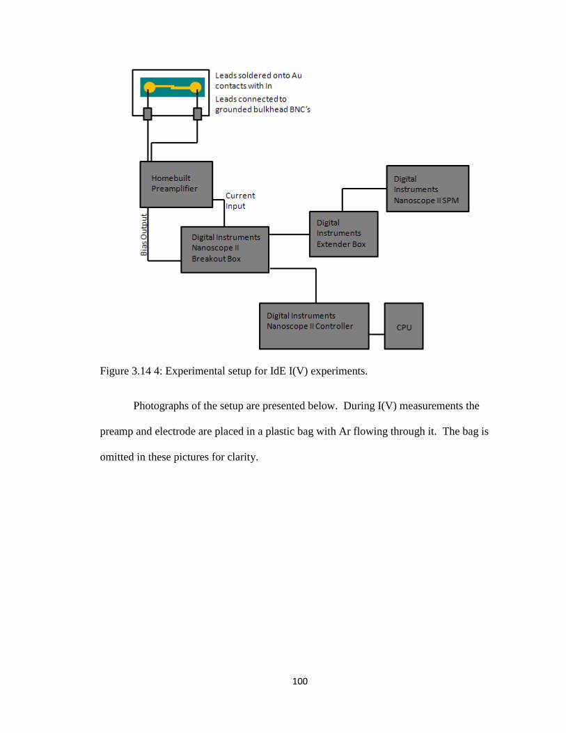
100
Figure 3.14 4: Experimental setup for IdE I(V) experiments.
Photographs of the setup are presented below. During I(V) measurements the
preamp and electrode are placed in a plastic bag with Ar flowing through it. The bag is
omitted in these pictures for clarity.
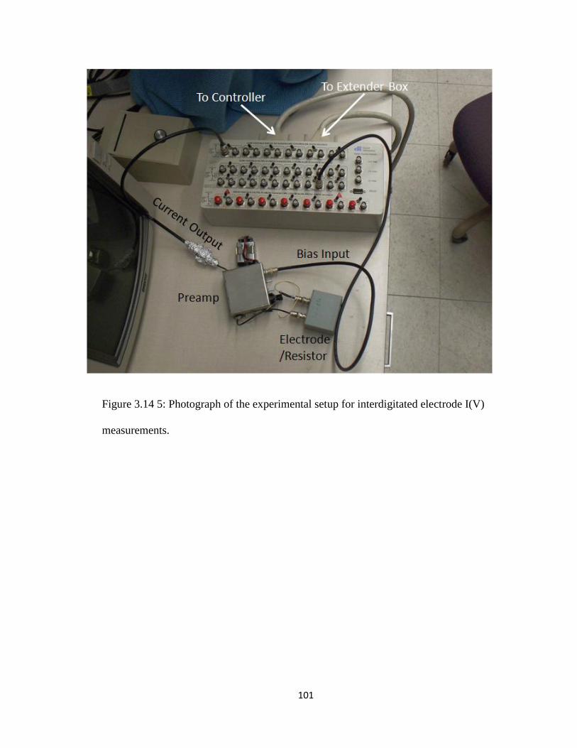
101
Figure 3.14 5: Photograph of the experimental setup for interdigitated electrode I(V)
measurements.
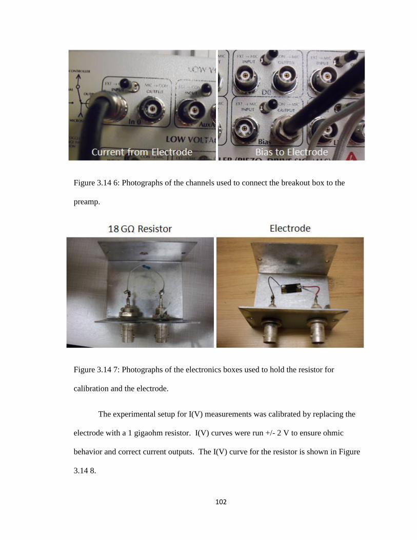
102
Figure 3.14 6: Photographs of the channels used to connect the breakout box to the
preamp.
Figure 3.14 7: Photographs of the electronics boxes used to hold the resistor for
calibration and the electrode.
The experimental setup for I(V) measurements was calibrated by replacing the
electrode with a 1 gigaohm resistor. I(V) curves were run +/- 2 V to ensure ohmic
behavior and correct current outputs. The I(V) curve for the resistor is shown in Figure
3.14 8.
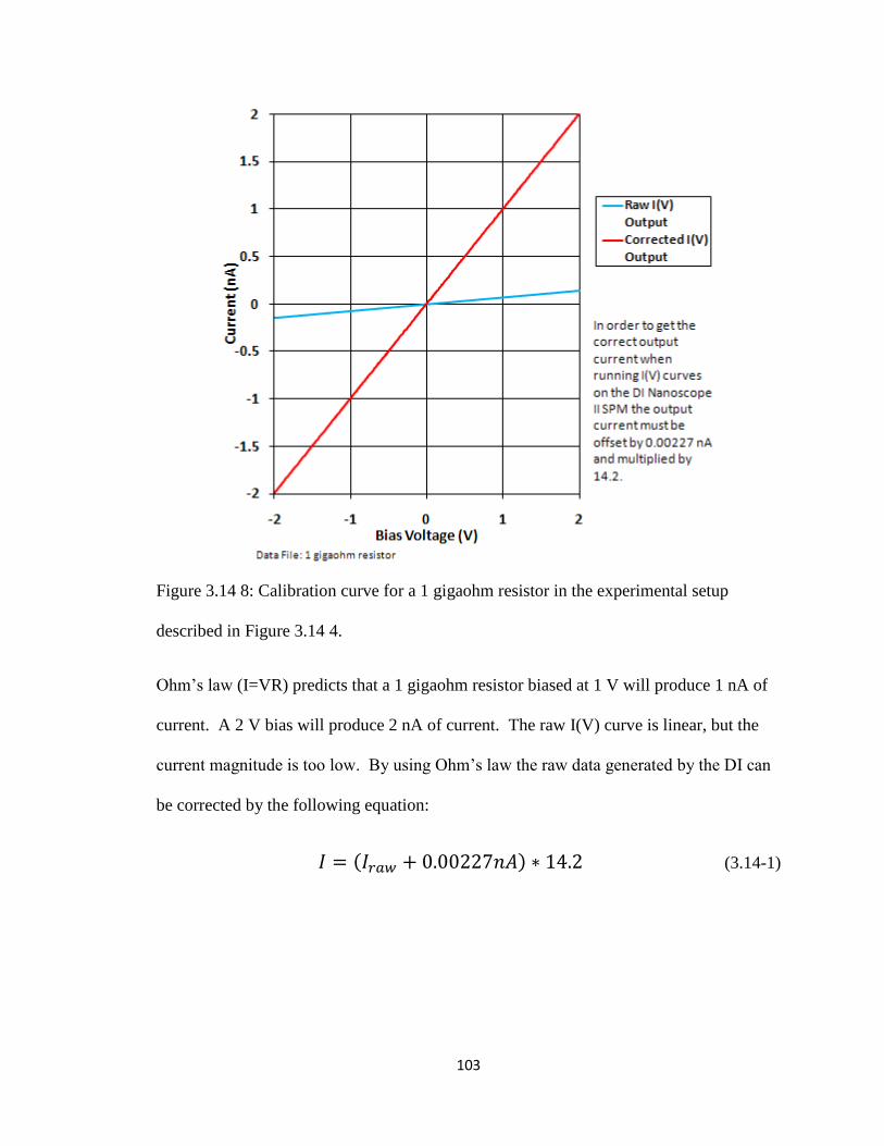
103
Figure 3.14 8: Calibration curve for a 1 gigaohm resistor in the experimental setup
described in Figure 3.14 4.
Ohm‟s law (I=VR) predicts that a 1 gigaohm resistor biased at 1 V will produce 1 nA of
current. A 2 V bias will produce 2 nA of current. The raw I(V) curve is linear, but the
current magnitude is too low. By using Ohm‟s law the raw data generated by the DI can
be corrected by the following equation:
(3.14-1)

104
Where I is the corrected current output and Iraw is the raw current output from the DI.
Once this correction is applied the 1 gigaohm resistor I(V) curve (Figure 3.14 8 red trace)
exhibits the correct values.
105
Chapter 4: Results and Discussion
4.1 Characterization of Tetrasulfonatophenyl Porphyrin and its Aggregate by UV-
visible and Resonance Light Scattering Spectroscopy
Because of its high extinction coefficient solutions of TSPP are highly colored.
The intense color of the porphyrin solution makes UV-visible and RSL suitable
techniques for studying the aggregation of H2(H4TSPP). The UV-visible spectrum of
monomeric (H2TSPP)4-
(free base form) shows a strong Soret or B-band at 413 nm and
four smaller Q-bands at 514 nm, 550 nm, 578 nm, and 638 nm. As its name implies free
base (H2TSPP)4-
exists primarily in basic solutions. As solution pH is lowered the free
base macrocycle is protonated in two steps. The first species formed is the monoacid
(H3TSPP)3-
(pKa= 6.061
). Further addition of protons converts the monoacid to the diacid
(H4TSPP)2-
(pKa=4.561
). The diacid UV-visible spectrum shows a Soret band red shifted
relative to the free base at 434 nm and two Q-bands at 595 nm and 644 nm.
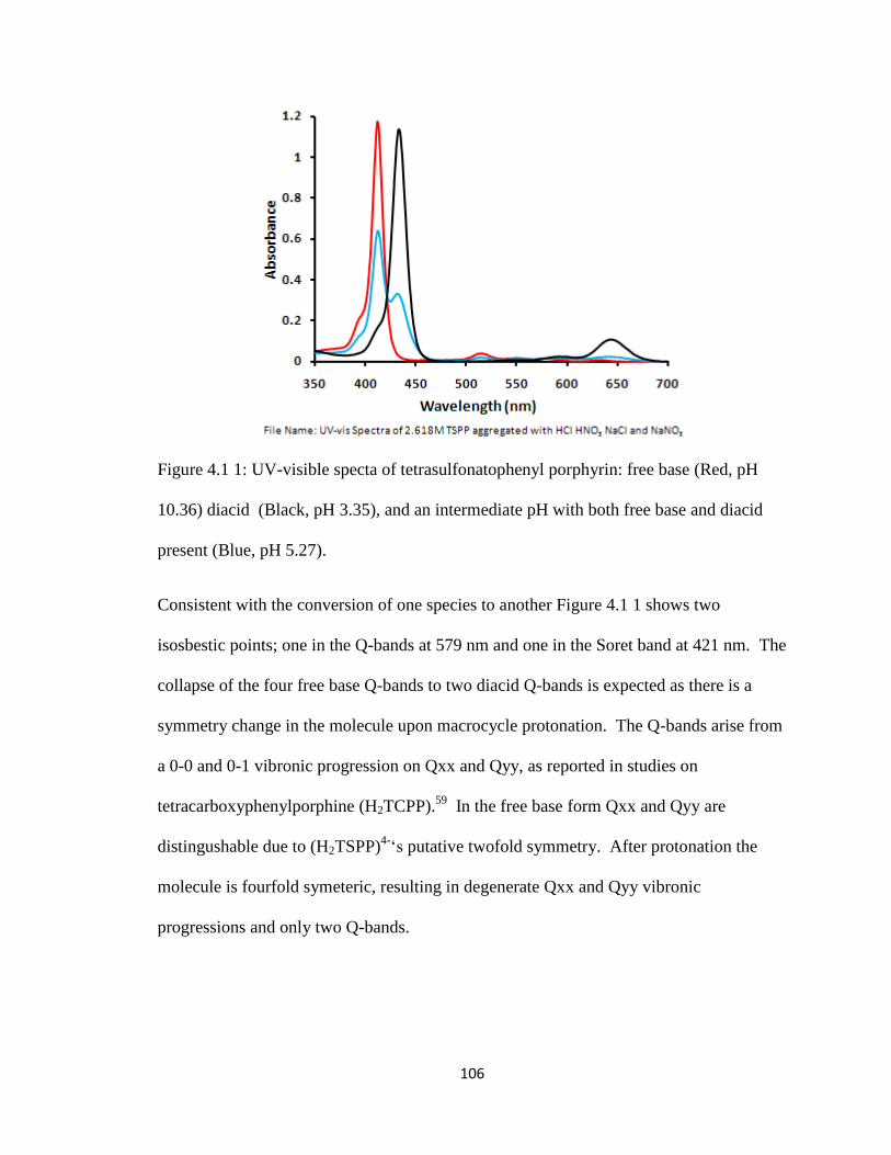
106
Figure 4.1 1: UV-visible specta of tetrasulfonatophenyl porphyrin: free base (Red, pH
10.36) diacid (Black, pH 3.35), and an intermediate pH with both free base and diacid
present (Blue, pH 5.27).
Consistent with the conversion of one species to another Figure 4.1 1 shows two
isosbestic points; one in the Q-bands at 579 nm and one in the Soret band at 421 nm. The
collapse of the four free base Q-bands to two diacid Q-bands is expected as there is a
symmetry change in the molecule upon macrocycle protonation. The Q-bands arise from
a 0-0 and 0-1 vibronic progression on Qxx and Qyy, as reported in studies on
tetracarboxyphenylporphine (H2TCPP).59
In the free base form Qxx and Qyy are
distingushable due to (H2TSPP)4-„s putative twofold symmetry. After protonation the
molecule is fourfold symeteric, resulting in degenerate Qxx and Qyy vibronic
progressions and only two Q-bands.
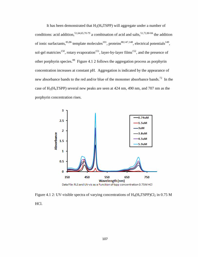
107
It has been demonstrated that H2(H4TSPP) will aggregate under a number of
conditions: acid addition,51,64,65,70-79
a combination of acid and salts,51,72,80-84
the addition
of ionic surfactants,85,86
template molecules101
, proteins88,147,148
, electrical potentials149
,
sol-gel matricies150
, rotary evaporation151
, layer-by-layer films152
, and the presence of
other porphyrin species.88
Figure 4.1 2 follows the aggregation process as porphyrin
concentration increases at constant pH. Aggregation is indicated by the appearance of
new absorbance bands to the red and/or blue of the monomer absorbance bands.72
In the
case of H2(H4TSPP) several new peaks are seen at 424 nm, 490 nm, and 707 nm as the
porphyrin concentration rises.
Figure 4.1 2: UV-visible spectra of varying concentrations of H4(H4TSPP)Cl2 in 0.75 M
HCl.
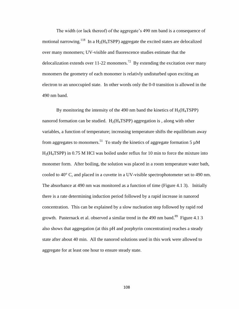
108
The width (or lack thereof) of the aggregate‟s 490 nm band is a consequence of
motional narrowing.118
In a H2(H4TSPP) aggregate the excited states are delocalized
over many monomers; UV-visible and fluorescence studies estimate that the
delocalization extends over 11-22 monomers.72
By extending the excitation over many
monomers the geometry of each monomer is relativly undisturbed upon exciting an
electron to an unoccupied state. In other words only the 0-0 transition is allowed in the
490 nm band.
By monitoring the intensity of the 490 nm band the kinetics of H2(H4TSPP)
nanorod formation can be studied. H2(H4TSPP) aggregation is , along with other
variables, a function of temperature; increasing temperature shifts the equilibrium away
from aggregates to monomers.51
To study the kinetics of aggregate formation 5 µM
H2(H4TSPP) in 0.75 M HCl was boiled under reflux for 10 min to force the mixture into
monomer form. After boiling, the solution was placed in a room temperature water bath,
cooled to 40° C, and placed in a cuvette in a UV-visible spectrophotometer set to 490 nm.
The absorbance at 490 nm was monitored as a function of time (Figure 4.1 3). Initially
there is a rate determining induction period followed by a rapid increase in nanorod
concentration. This can be explained by a slow nucleation step followed by rapid rod
growth. Pasternack et al. observed a similar trend in the 490 nm band.89
Figure 4.1 3
also shows that aggregation (at this pH and porphyrin concentration) reaches a steady
state after about 40 min. All the nanorod solutions used in this work were allowed to
aggregate for at least one hour to ensure steady state.
109
Figure 4.1 3: Graph of absorbance at 490 nm vs. time during nanorod formation.
It is reasonable to ask if the aggregation process is an irreversible chemical
reaction as opposed to the formation of a supramolecular aggregate where the structure of
the individual monomers is intact. To investigate this question we prepared a solution of
nanorods, charaterized it by UV-visible spectroscopy, then added NaOH to the solution
until the pH reached 10.32. Figure 4.1 4 compares the nanorod spectrum, the spectrum of
the basified nanorods, and a control spectrum of free base (H2TSPP)4-
at pH 10.00. Aside
from broadening in the basified nanorods the control and basified spectra are identical
indicating that aggregation is reversible and nondestructive to the monomers.
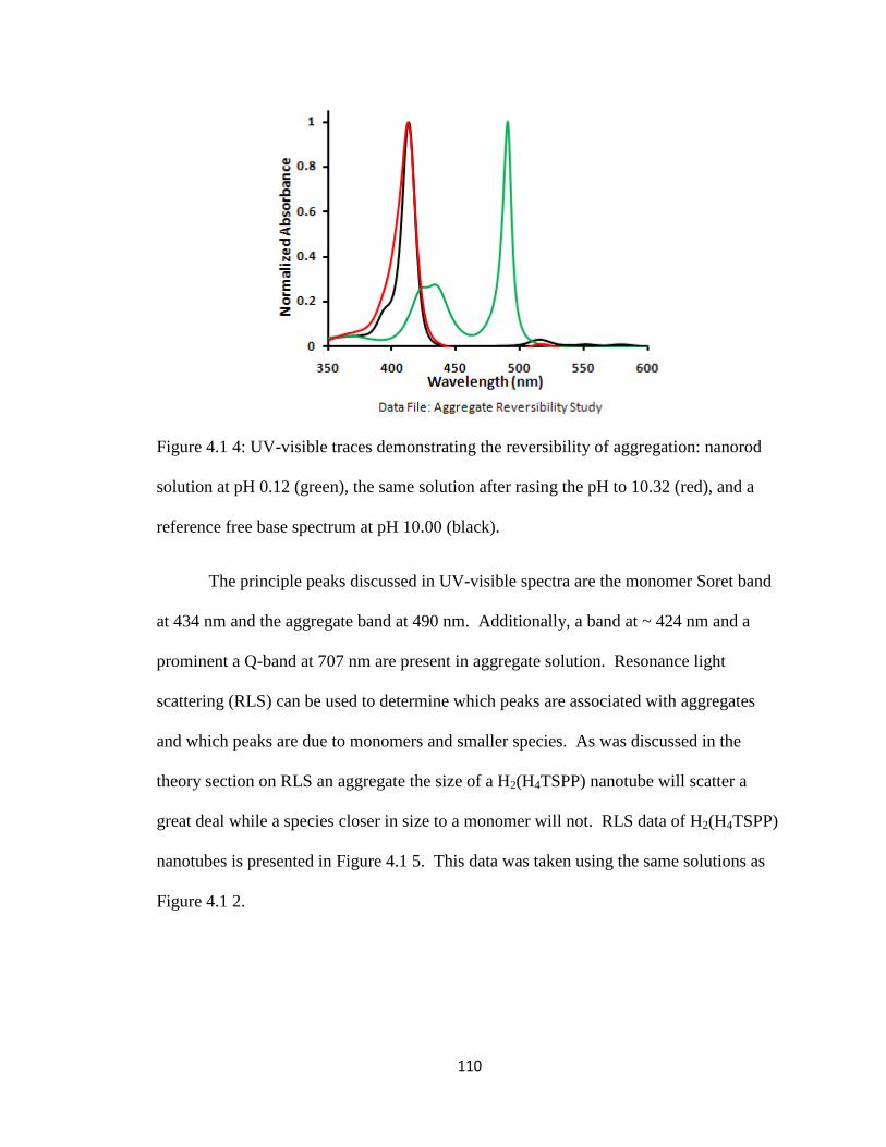
110
Figure 4.1 4: UV-visible traces demonstrating the reversibility of aggregation: nanorod
solution at pH 0.12 (green), the same solution after rasing the pH to 10.32 (red), and a
reference free base spectrum at pH 10.00 (black).
The principle peaks discussed in UV-visible spectra are the monomer Soret band
at 434 nm and the aggregate band at 490 nm. Additionally, a band at ~ 424 nm and a
prominent a Q-band at 707 nm are present in aggregate solution. Resonance light
scattering (RLS) can be used to determine which peaks are associated with aggregates
and which peaks are due to monomers and smaller species. As was discussed in the
theory section on RLS an aggregate the size of a H2(H4TSPP) nanotube will scatter a
great deal while a species closer in size to a monomer will not. RLS data of H2(H4TSPP)
nanotubes is presented in Figure 4.1 5. This data was taken using the same solutions as
Figure 4.1 2.
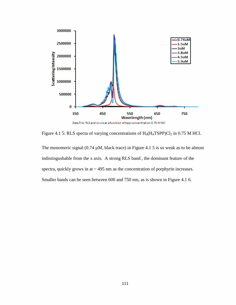
111
Figure 4.1 5: RLS specta of varying concentrations of H4(H4TSPP)Cl2 in 0.75 M HCl.
The monomeric signal (0.74 µM, black trace) in Figure 4.1 5 is so weak as to be almost
indistingushable from the x axis. A strong RLS band , the dominant feature of the
spectra, quickly grows in at ~ 495 nm as the concentration of porphyrin increases.
Smaller bands can be seen between 600 and 750 nm, as is shown in Figure 4.1 6.
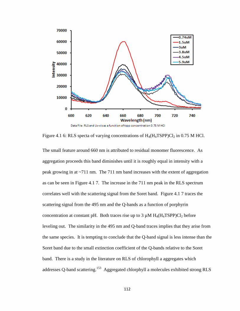
112
Figure 4.1 6: RLS specta of varying concentrations of H4(H4TSPP)Cl2 in 0.75 M HCl.
The small feature around 660 nm is attributed to residual monomer fluorescence. As
aggregation proceeds this band diminishes until it is roughly equal in intensity with a
peak growing in at ~711 nm. The 711 nm band increases with the extent of aggregation
as can be seen in Figure 4.1 7. The increase in the 711 nm peak in the RLS spectrum
correlates well with the scattering signal from the Soret band. Figure 4.1 7 traces the
scattering signal from the 495 nm and the Q-bands as a function of porphyrin
concentration at constant pH. Both traces rise up to 3 µM H4(H4TSPP)Cl2 before
leveling out. The similarity in the 495 nm and Q-band traces implies that they arise from
the same species. It is tempting to conclude that the Q-band signal is less intense than the
Soret band due to the small extinction coefficient of the Q-bands relative to the Soret
band. There is a study in the literature on RLS of chlorophyll a aggregates which
addresses Q-band scattering.153
Aggregated chlorphyll a molecules exhibited strong RLS
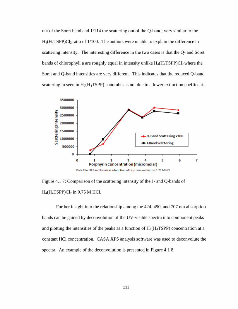
113
out of the Soret band and 1/114 the scattering out of the Q-band; very similar to the
H4(H4TSPP)Cl2 ratio of 1/100. The authors were unable to explain the difference in
scattering intensity. The interesting difference in the two cases is that the Q- and Soret
bands of chlorophyll a are roughly equal in intensity unlike H4(H4TSPP)Cl2 where the
Soret and Q-band intensities are very different. This indicates that the reduced Q-band
scattering in seen in H2(H4TSPP) nanotubes is not due to a lower extinction coefficent.
Figure 4.1 7: Comparison of the scattering intensity of the J- and Q-bands of
H4(H4TSPP)Cl2 in 0.75 M HCl.
Further insight into the relationship among the 424, 490, and 707 nm absorption
bands can be gained by deconvolution of the UV-visible spectra into component peaks
and plotting the intensities of the peaks as a function of H2(H4TSPP) concentration at a
constant HCl concentration. CASA XPS analysis software was used to deconvolute the
spectra. An example of the deconvolution is presented in Figure 4.1 8.
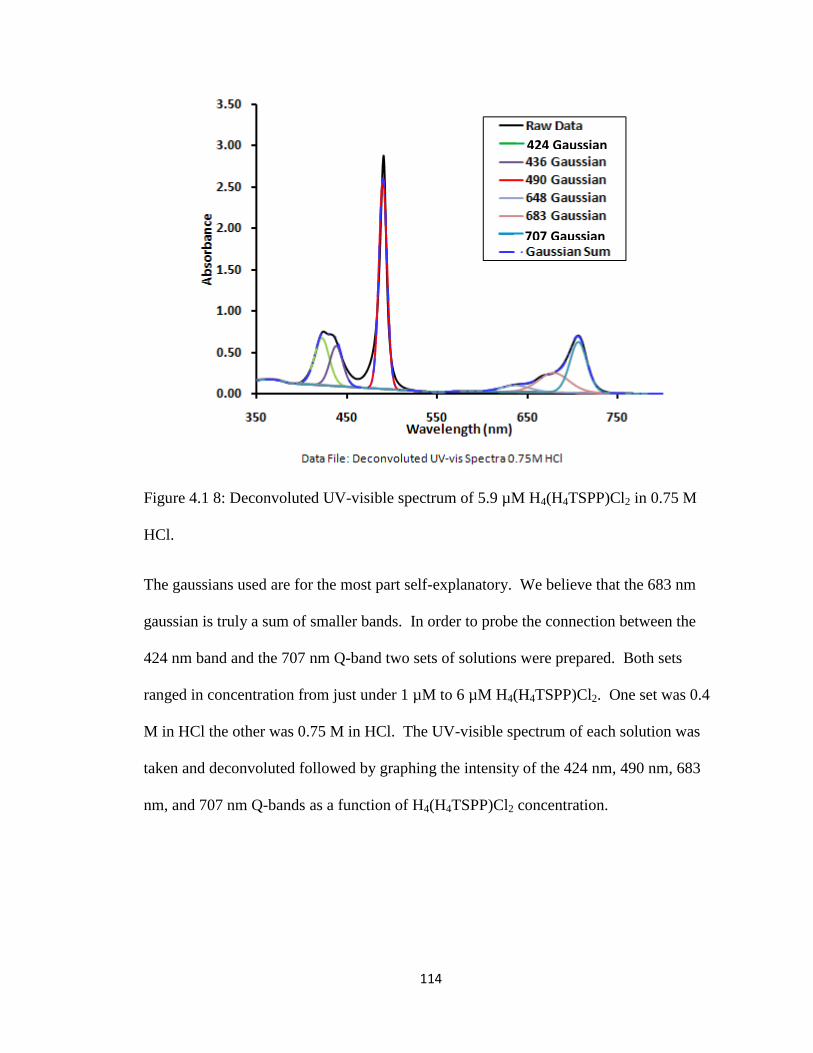
114
Figure 4.1 8: Deconvoluted UV-visible spectrum of 5.9 µM H4(H4TSPP)Cl2 in 0.75 M
HCl.
The gaussians used are for the most part self-explanatory. We believe that the 683 nm
gaussian is truly a sum of smaller bands. In order to probe the connection between the
424 nm band and the 707 nm Q-band two sets of solutions were prepared. Both sets
ranged in concentration from just under 1 µM to 6 µM H4(H4TSPP)Cl2. One set was 0.4
M in HCl the other was 0.75 M in HCl. The UV-visible spectrum of each solution was
taken and deconvoluted followed by graphing the intensity of the 424 nm, 490 nm, 683
nm, and 707 nm Q-bands as a function of H4(H4TSPP)Cl2 concentration.
424 Gaussian
707 Gaussian
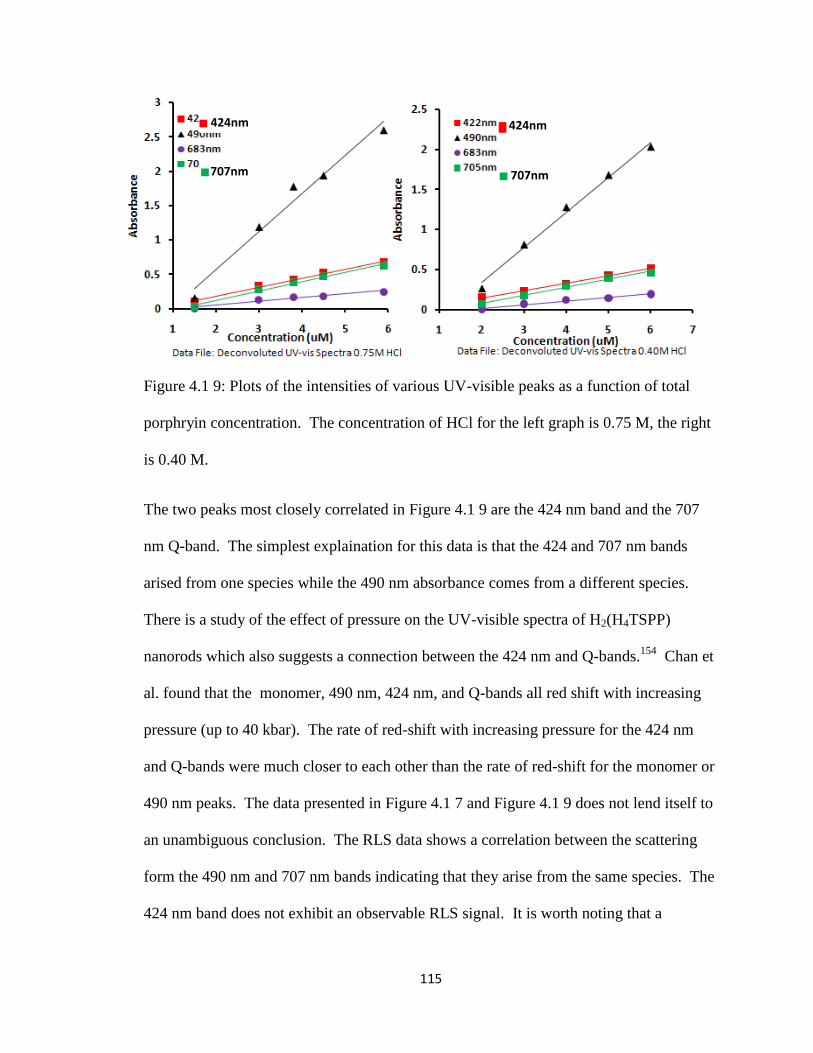
115
Figure 4.1 9: Plots of the intensities of various UV-visible peaks as a function of total
porphryin concentration. The concentration of HCl for the left graph is 0.75 M, the right
is 0.40 M.
The two peaks most closely correlated in Figure 4.1 9 are the 424 nm band and the 707
nm Q-band. The simplest explaination for this data is that the 424 and 707 nm bands
arised from one species while the 490 nm absorbance comes from a different species.
There is a study of the effect of pressure on the UV-visible spectra of H2(H4TSPP)
nanorods which also suggests a connection between the 424 nm and Q-bands.154
Chan et
al. found that the monomer, 490 nm, 424 nm, and Q-bands all red shift with increasing
pressure (up to 40 kbar). The rate of red-shift with increasing pressure for the 424 nm
and Q-bands were much closer to each other than the rate of red-shift for the monomer or
490 nm peaks. The data presented in Figure 4.1 7 and Figure 4.1 9 does not lend itself to
an unambiguous conclusion. The RLS data shows a correlation between the scattering
form the 490 nm and 707 nm bands indicating that they arise from the same species. The
424 nm band does not exhibit an observable RLS signal. It is worth noting that a
424nm 424nm
707nm 707nm
116
scattering peak of comparable intensity to the 711 nm peak could be obscured by the dip
in RLS spectrum due to monomer absorbance. The RLS data seems to show that the 707
nm and 490 nm absorbance bands arise from the same species, while the data is not clear
with respect to the 424 nm band. The 424 nm band‟s scattering intensity may be too low
to observe or there may be no signal at all. Based upon RLS data we can not assign the
424 nm band. The peak height vs. concentration data indicates that the 424 nm and 707
nm bands grow in at the same rate with the 490 nm band growing in much faster. This
data suggests that the 490 nm species is different from the species which is responsible
for the 424 and 707 nm bands. Both the 424 and 490 nm bands can be connected to the
707 nm band through UV-visible and RLS data respectivly, but we have not been able to
directly connect the 424 and 490 nm bands. Based upon the data presented here we can
not unambiguoulsy assign the aggregate peaks in the UV-visible and RLS spectra,
although some tennative conclusions can be drawn. It is certain that the 490 nm peak
belongs to the nanotubes because of its strong RLS signal. The assignments of the 424
nm and 707 nm peaks are uncertain because of the conflicting RLS and UV-visible data.
Since the main focus of this work is charaterizing H2(H4TSPP) nanorods
deposited on substrates UV-visible spectra of free base, diacid and aggregated
H2(H4TSPP) deposited on quartz plates were recorded to evaluate the effects of
deposition on the molecule in its different forms. The free base and diacid data is
displayed in Figure 4.1 10.
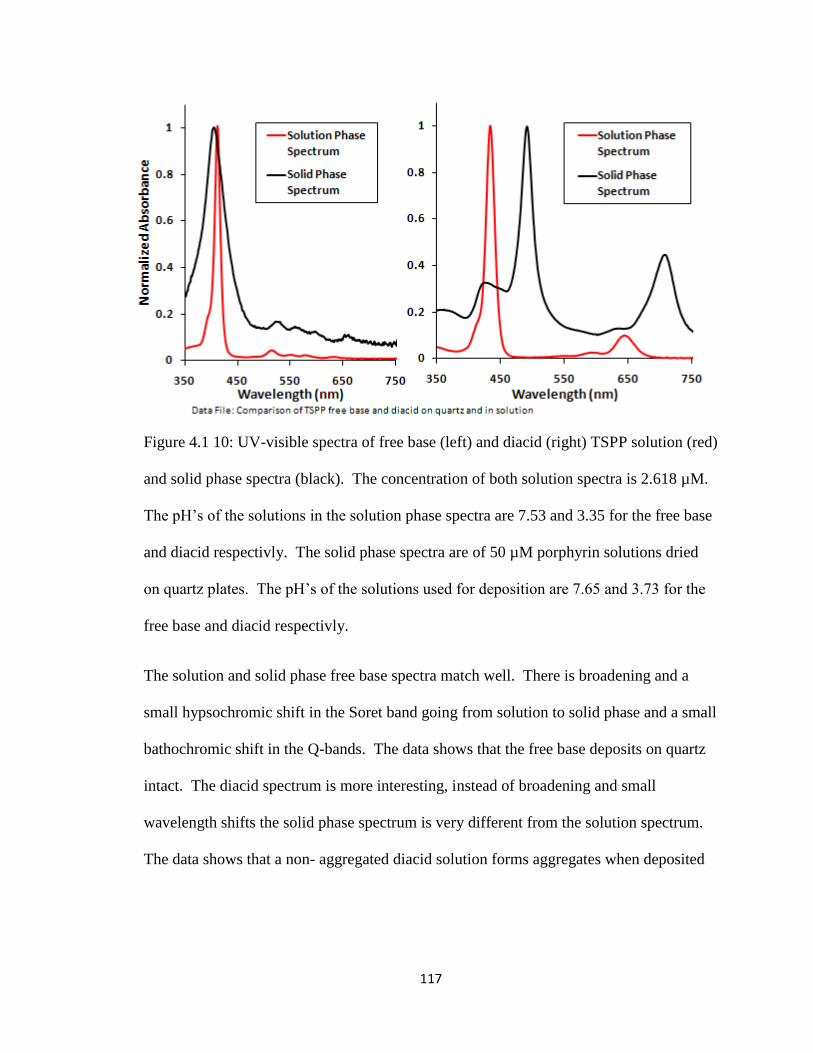
117
Figure 4.1 10: UV-visible spectra of free base (left) and diacid (right) TSPP solution (red)
and solid phase spectra (black). The concentration of both solution spectra is 2.618 µM.
The pH‟s of the solutions in the solution phase spectra are 7.53 and 3.35 for the free base
and diacid respectivly. The solid phase spectra are of 50 µM porphyrin solutions dried
on quartz plates. The pH‟s of the solutions used for deposition are 7.65 and 3.73 for the
free base and diacid respectivly.
The solution and solid phase free base spectra match well. There is broadening and a
small hypsochromic shift in the Soret band going from solution to solid phase and a small
bathochromic shift in the Q-bands. The data shows that the free base deposits on quartz
intact. The diacid spectrum is more interesting, instead of broadening and small
wavelength shifts the solid phase spectrum is very different from the solution spectrum.
The data shows that a non- aggregated diacid solution forms aggregates when deposited
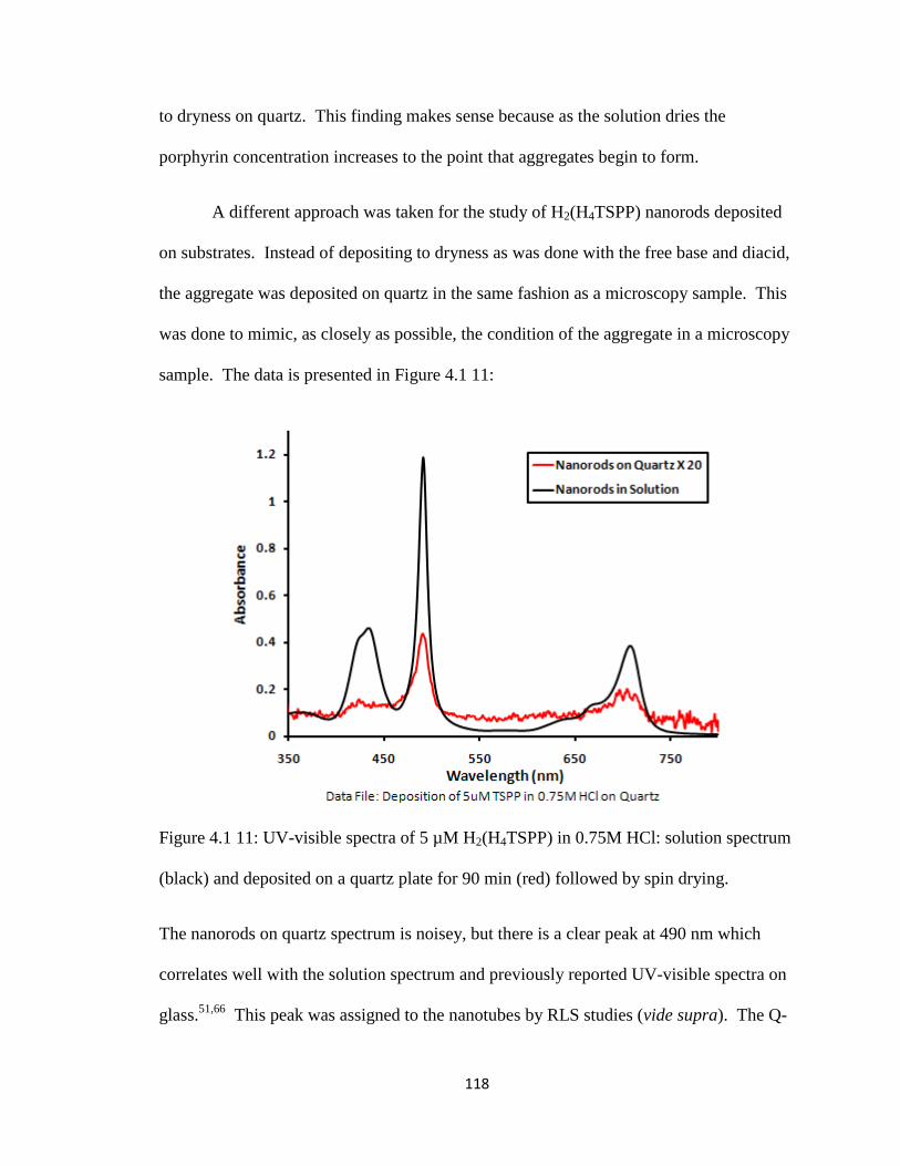
118
to dryness on quartz. This finding makes sense because as the solution dries the
porphyrin concentration increases to the point that aggregates begin to form.
A different approach was taken for the study of H2(H4TSPP) nanorods deposited
on substrates. Instead of depositing to dryness as was done with the free base and diacid,
the aggregate was deposited on quartz in the same fashion as a microscopy sample. This
was done to mimic, as closely as possible, the condition of the aggregate in a microscopy
sample. The data is presented in Figure 4.1 11:
Figure 4.1 11: UV-visible spectra of 5 µM H2(H4TSPP) in 0.75M HCl: solution spectrum
(black) and deposited on a quartz plate for 90 min (red) followed by spin drying.
The nanorods on quartz spectrum is noisey, but there is a clear peak at 490 nm which
correlates well with the solution spectrum and previously reported UV-visible spectra on
glass.51,66
This peak was assigned to the nanotubes by RLS studies (vide supra). The Q-
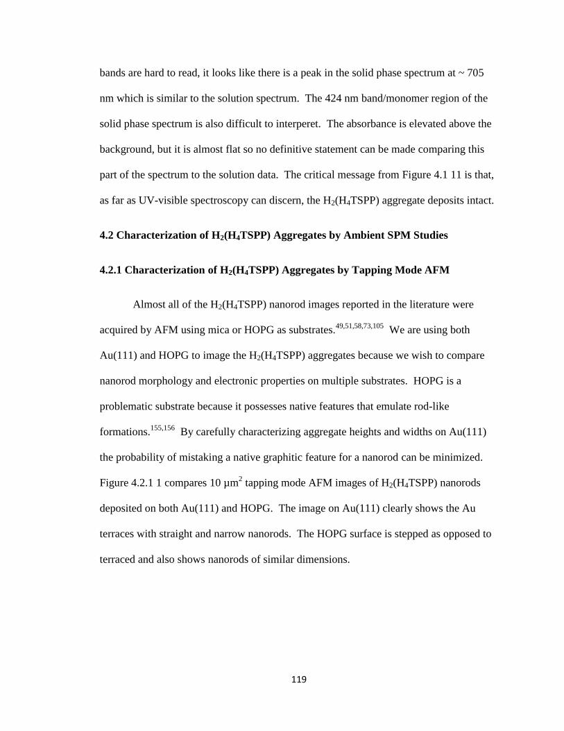
119
bands are hard to read, it looks like there is a peak in the solid phase spectrum at ~ 705
nm which is similar to the solution spectrum. The 424 nm band/monomer region of the
solid phase spectrum is also difficult to interperet. The absorbance is elevated above the
background, but it is almost flat so no definitive statement can be made comparing this
part of the spectrum to the solution data. The critical message from Figure 4.1 11 is that,
as far as UV-visible spectroscopy can discern, the H2(H4TSPP) aggregate deposits intact.
4.2 Characterization of H2(H4TSPP) Aggregates by Ambient SPM Studies
4.2.1 Characterization of H2(H4TSPP) Aggregates by Tapping Mode AFM
Almost all of the H2(H4TSPP) nanorod images reported in the literature were
acquired by AFM using mica or HOPG as substrates.49,51,58,73,105
We are using both
Au(111) and HOPG to image the H2(H4TSPP) aggregates because we wish to compare
nanorod morphology and electronic properties on multiple substrates. HOPG is a
problematic substrate because it possesses native features that emulate rod-like
formations.155,156
By carefully characterizing aggregate heights and widths on Au(111)
the probability of mistaking a native graphitic feature for a nanorod can be minimized.
Figure 4.2.1 1 compares 10 µm2 tapping mode AFM images of H2(H4TSPP) nanorods
deposited on both Au(111) and HOPG. The image on Au(111) clearly shows the Au
terraces with straight and narrow nanorods. The HOPG surface is stepped as opposed to
terraced and also shows nanorods of similar dimensions.
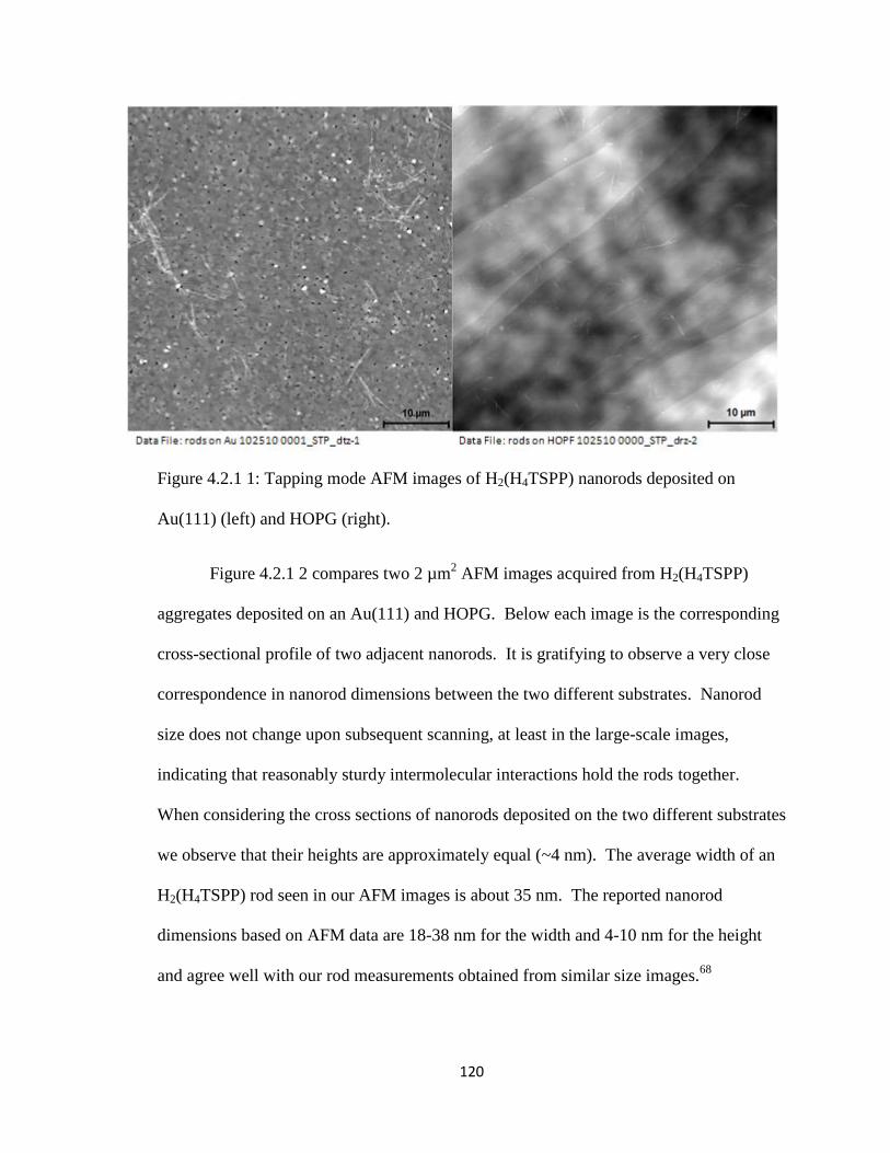
120
Figure 4.2.1 1: Tapping mode AFM images of H2(H4TSPP) nanorods deposited on
Au(111) (left) and HOPG (right).
Figure 4.2.1 2 compares two 2 µm2 AFM images acquired from H2(H4TSPP)
aggregates deposited on an Au(111) and HOPG. Below each image is the corresponding
cross-sectional profile of two adjacent nanorods. It is gratifying to observe a very close
correspondence in nanorod dimensions between the two different substrates. Nanorod
size does not change upon subsequent scanning, at least in the large-scale images,
indicating that reasonably sturdy intermolecular interactions hold the rods together.
When considering the cross sections of nanorods deposited on the two different substrates
we observe that their heights are approximately equal (~4 nm). The average width of an
H2(H4TSPP) rod seen in our AFM images is about 35 nm. The reported nanorod
dimensions based on AFM data are 18-38 nm for the width and 4-10 nm for the height
and agree well with our rod measurements obtained from similar size images.68
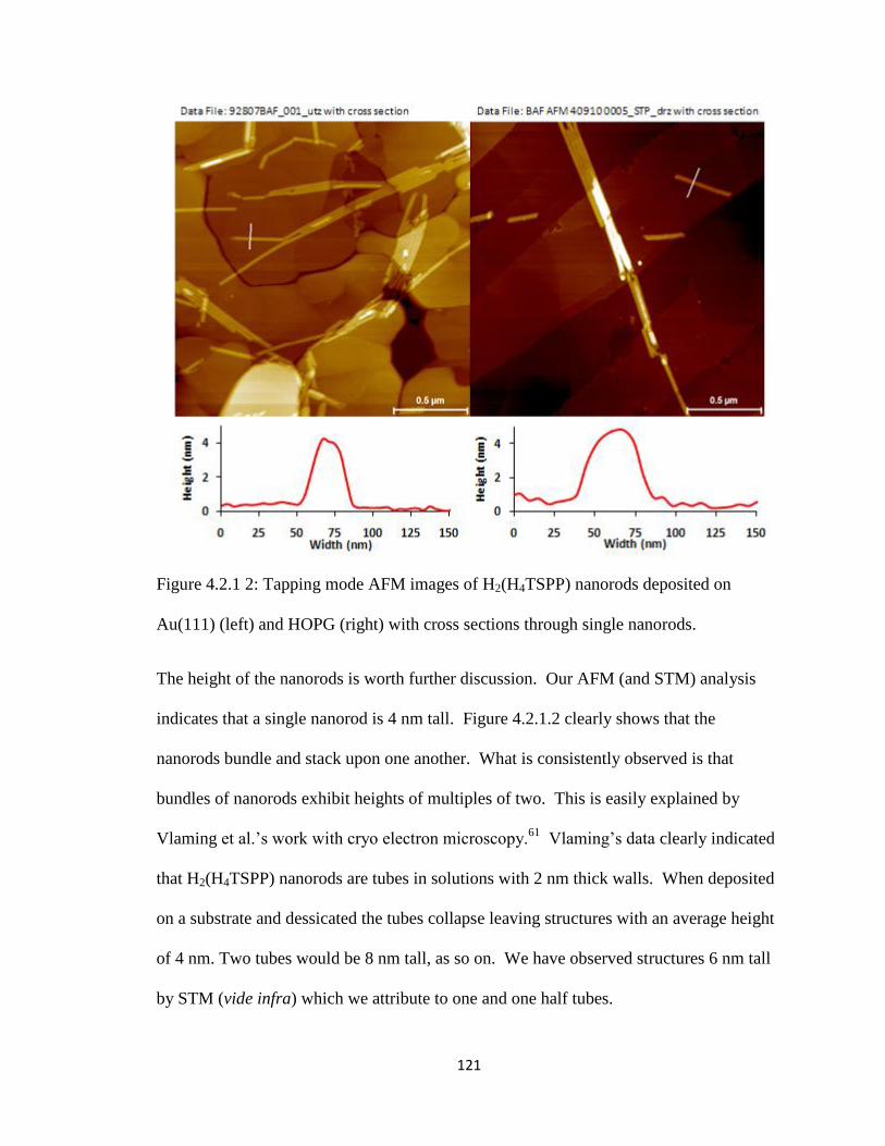
121
Figure 4.2.1 2: Tapping mode AFM images of H2(H4TSPP) nanorods deposited on
Au(111) (left) and HOPG (right) with cross sections through single nanorods.
The height of the nanorods is worth further discussion. Our AFM (and STM) analysis
indicates that a single nanorod is 4 nm tall. Figure 4.2.1.2 clearly shows that the
nanorods bundle and stack upon one another. What is consistently observed is that
bundles of nanorods exhibit heights of multiples of two. This is easily explained by
Vlaming et al.‟s work with cryo electron microscopy.61
Vlaming‟s data clearly indicated
that H2(H4TSPP) nanorods are tubes in solutions with 2 nm thick walls. When deposited
on a substrate and dessicated the tubes collapse leaving structures with an average height
of 4 nm. Two tubes would be 8 nm tall, as so on. We have observed structures 6 nm tall
by STM (vide infra) which we attribute to one and one half tubes.
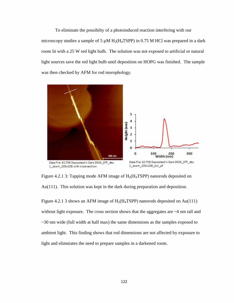
122
To eliminate the possibilty of a photoinduced reaction interfering with our
microscopy studies a sample of 5 µM H2(H4TSPP) in 0.75 M HCl was prepared in a dark
room lit with a 25 W red light bulb. The solution was not exposed to artificial or natural
light sources save the red light bulb until deposition on HOPG was finished. The sample
was then checked by AFM for rod morophology.
Figure 4.2.1 3: Tapping mode AFM image of H2(H4TSPP) nanorods deposited on
Au(111). This solution was kept in the dark during preparation and deposition.
Figure 4.2.1 3 shows an AFM image of H2(H4TSPP) nanorods deposited on Au(111)
without light exposure. The cross section shows that the aggregates are ~4 nm tall and
~30 nm wide (full width at half max) the same dimensions as the samples exposed to
ambient light. This finding shows that rod dimensions are not affected by exposure to
light and elimniates the need to prepare samples in a darkened room.
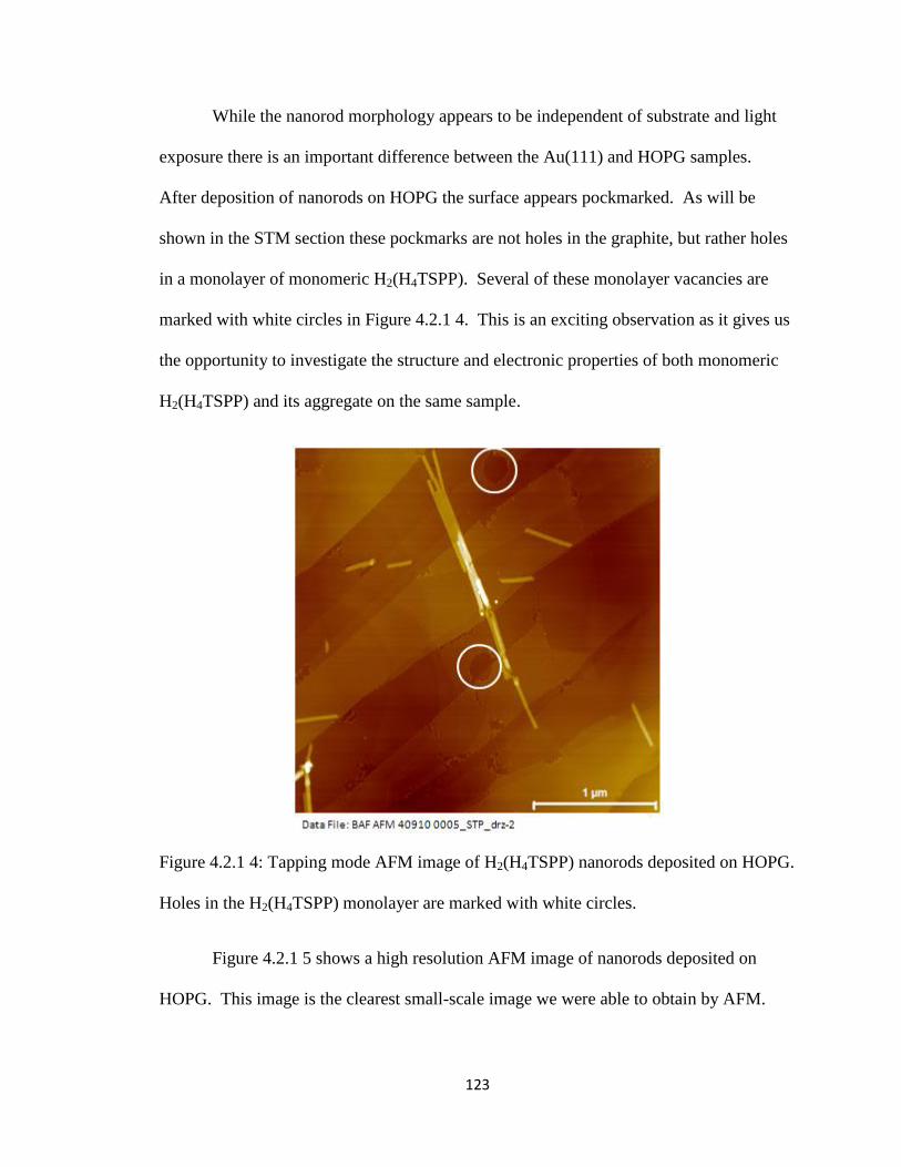
123
While the nanorod morphology appears to be independent of substrate and light
exposure there is an important difference between the Au(111) and HOPG samples.
After deposition of nanorods on HOPG the surface appears pockmarked. As will be
shown in the STM section these pockmarks are not holes in the graphite, but rather holes
in a monolayer of monomeric H2(H4TSPP). Several of these monolayer vacancies are
marked with white circles in Figure 4.2.1 4. This is an exciting observation as it gives us
the opportunity to investigate the structure and electronic properties of both monomeric
H2(H4TSPP) and its aggregate on the same sample.
Figure 4.2.1 4: Tapping mode AFM image of H2(H4TSPP) nanorods deposited on HOPG.
Holes in the H2(H4TSPP) monolayer are marked with white circles.
Figure 4.2.1 5 shows a high resolution AFM image of nanorods deposited on
HOPG. This image is the clearest small-scale image we were able to obtain by AFM.
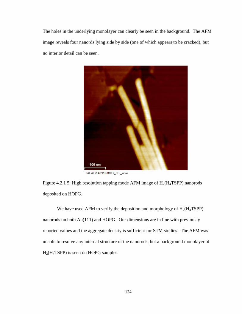
124
The holes in the underlying monolayer can clearly be seen in the background. The AFM
image reveals four nanords lying side by side (one of which appears to be cracked), but
no interior detail can be seen.
Figure 4.2.1 5: High resolution tapping mode AFM image of H2(H4TSPP) nanorods
deposited on HOPG.
We have used AFM to verify the deposition and morphology of H2(H4TSPP)
nanorods on both Au(111) and HOPG. Our dimensions are in line with previously
reported values and the aggregate density is sufficient for STM studies. The AFM was
unable to resolve any internal structure of the nanorods, but a background monolayer of
H2(H4TSPP) is seen on HOPG samples.
125
4.2.2 Characterization of H2(H4TSPP) Aggregates by Ambient Scanning Tunneling
Microscopy
As was stated in section 4.2.1 almost all of the H2(H4TSPP) nanorod images
reported in the literature were acquired by AFM using mica or HOPG as
substrates.49,51,58,73,105
We will use both Au(111) and HOPG to image the H2(H4TSPP)
aggregates because we wish to compare nanorod morphology and electronic properties
on multiple substrates. The goal of this study is to evaluate the accuracy of the staircase
model of aggregation and, if necessary, propose a new model of aggregate structure.
Because the nanorods are tall structures low tunneling currents and high sample biases
will be used to avoid crashing the tip into the nanorods.
Initially we will compare the results of our AFM study with STM images to
ensure good correlation between the two techniques. Figure 4.2.2 1 compares 1 μm2 size
AFM and STM images acquired from H2(H4TSPP) nanorods deposited on a Au(111)
substrate. Below each image is the corresponding cross-sectional profile of two adjacent
nanorods. It is gratifying to observe a very close correspondence between the AFM and
the STM images of H2(H4TSPP) nanorods, which appear as long straight features. The
gold terraces with single atomic steps are also observed in the images. The size of the
nanorods does not change considerably upon subsequent scanning, indicating that
reasonably sturdy intermolecular interactions hold the rods together. We note that
scanning under positive sample bias yields clear STM images. In reverse bias, it was
difficult to obtain well-resolved nanorod topography. This point is of prime importance
and will be discussed in detail in section 4.5.3.
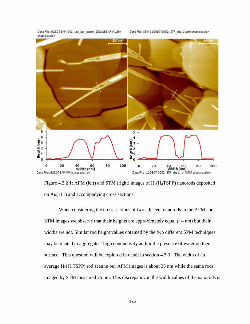
126
Figure 4.2.2 1: AFM (left) and STM (right) images of H2(H4TSPP) nanorods deposited
on Au(111) and accompanying cross sections.
When considering the cross sections of two adjacent nanorods in the AFM and
STM images we observe that their heights are approximately equal (~4 nm) but their
widths are not. Similar rod height values obtained by the two different SPM techniques
may be related to aggregates‟ high conductivity and/or the presence of water on their
surface. This question will be explored in detail in section 4.5.3. The width of an
average H2(H4TSPP) rod seen in our AFM images is about 35 nm while the same rods
imaged by STM measured 25 nm. This discrepancy in the width values of the nanorods is
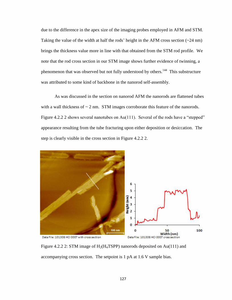
127
due to the difference in the apex size of the imaging probes employed in AFM and STM.
Taking the value of the width at half the rods‟ height in the AFM cross section (~24 nm)
brings the thickness value more in line with that obtained from the STM rod profile. We
note that the rod cross section in our STM image shows further evidence of twinning, a
phenomenon that was observed but not fully understood by others.144
This substructure
was attributed to some kind of backbone in the nanorod self-assembly.
As was discussed in the section on nanorod AFM the nanorods are flattened tubes
with a wall thickness of ~ 2 nm. STM images corroborate this feature of the nanorods.
Figure 4.2.2 2 shows several nanotubes on Au(111). Several of the rods have a “stepped”
appearance resulting from the tube fracturing upon either deposition or desiccation. The
step is clearly visible in the cross section in Figure 4.2.2 2.
Figure 4.2.2 2: STM image of H2(H4TSPP) nanorods deposited on Au(111) and
accompanying cross section. The setpoint is 1 pA at 1.6 V sample bias.
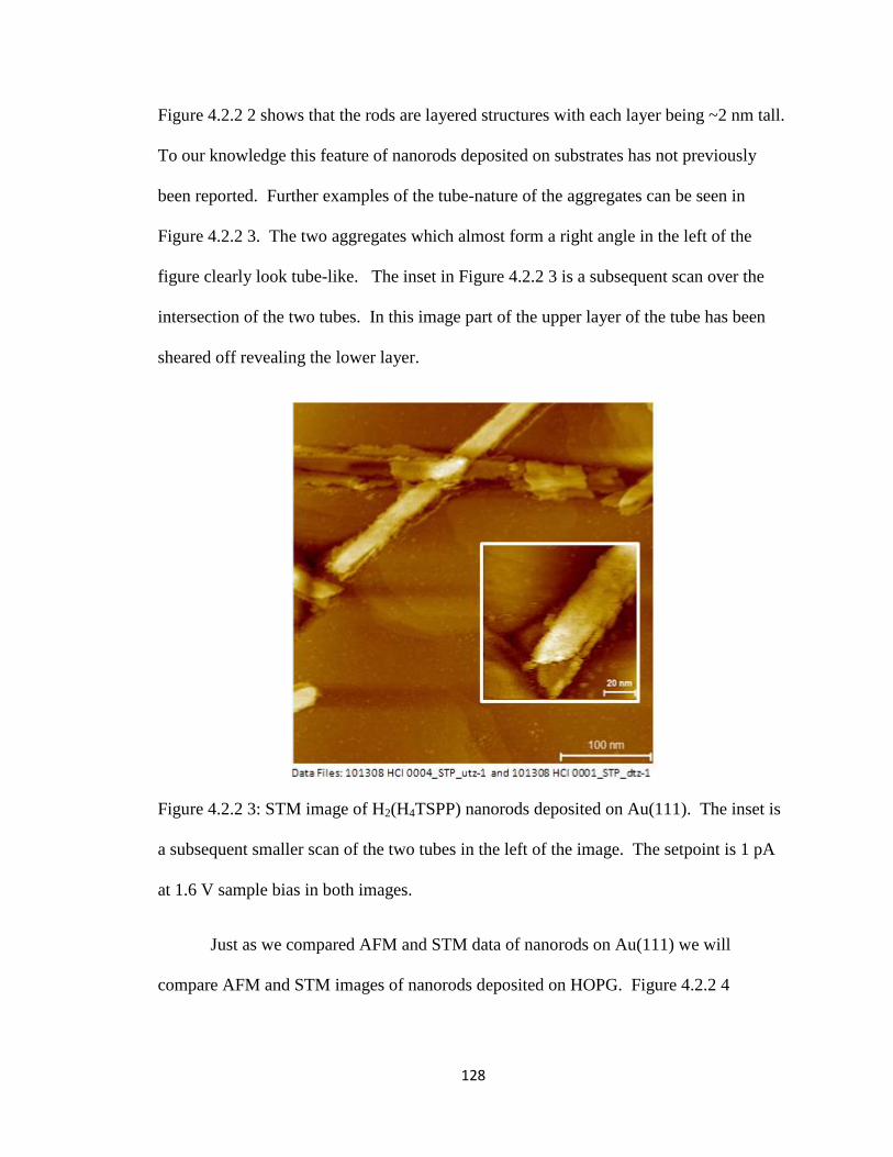
128
Figure 4.2.2 2 shows that the rods are layered structures with each layer being ~2 nm tall.
To our knowledge this feature of nanorods deposited on substrates has not previously
been reported. Further examples of the tube-nature of the aggregates can be seen in
Figure 4.2.2 3. The two aggregates which almost form a right angle in the left of the
figure clearly look tube-like. The inset in Figure 4.2.2 3 is a subsequent scan over the
intersection of the two tubes. In this image part of the upper layer of the tube has been
sheared off revealing the lower layer.
Figure 4.2.2 3: STM image of H2(H4TSPP) nanorods deposited on Au(111). The inset is
a subsequent smaller scan of the two tubes in the left of the image. The setpoint is 1 pA
at 1.6 V sample bias in both images.
Just as we compared AFM and STM data of nanorods on Au(111) we will
compare AFM and STM images of nanorods deposited on HOPG. Figure 4.2.2 4

129
compares 1 μm2 size AFM and STM images acquired from H2(H4TSPP) nanorods
deposited on HOPG. Below each image is the corresponding cross-sectional profile of
two adjacent nanorods. It is gratifying, just as with nanorods on Au(111) to observe a
very close correspondence between the AFM and the STM images of H2(H4TSPP)
nanorods. Also the nanorods on HOPG exhibit the layered structure previously described
for the rods on Au(111). Additionally, the monolayer of porphyrin monomers can be
seen in the background of both the AFM and STM images of rods on HOPG unlike the
case for rods on Au(111).
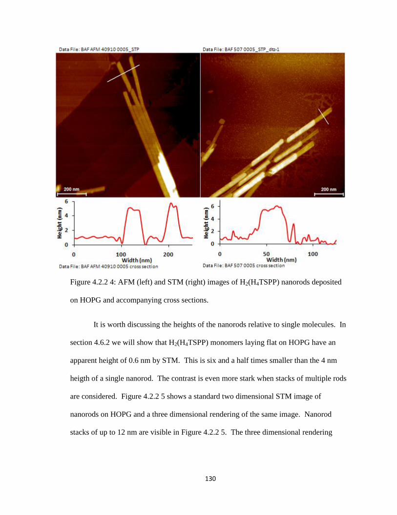
130
Figure 4.2.2 4: AFM (left) and STM (right) images of H2(H4TSPP) nanorods deposited
on HOPG and accompanying cross sections.
It is worth discussing the heights of the nanorods relative to single molecules. In
section 4.6.2 we will show that H2(H4TSPP) monomers laying flat on HOPG have an
apparent height of 0.6 nm by STM. This is six and a half times smaller than the 4 nm
heigth of a single nanorod. The contrast is even more stark when stacks of multiple rods
are considered. Figure 4.2.2 5 shows a standard two dimensional STM image of
nanorods on HOPG and a three dimensional rendering of the same image. Nanorod
stacks of up to 12 nm are visible in Figure 4.2.2 5. The three dimensional rendering
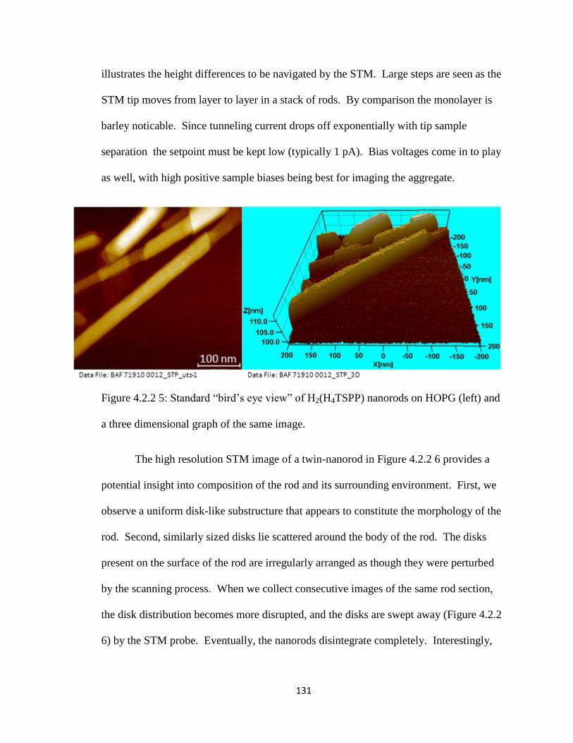
131
illustrates the height differences to be navigated by the STM. Large steps are seen as the
STM tip moves from layer to layer in a stack of rods. By comparison the monolayer is
barley noticable. Since tunneling current drops off exponentially with tip sample
separation the setpoint must be kept low (typically 1 pA). Bias voltages come in to play
as well, with high positive sample biases being best for imaging the aggregate.
Figure 4.2.2 5: Standard “bird‟s eye view” of H2(H4TSPP) nanorods on HOPG (left) and
a three dimensional graph of the same image.
The high resolution STM image of a twin-nanorod in Figure 4.2.2 6 provides a
potential insight into composition of the rod and its surrounding environment. First, we
observe a uniform disk-like substructure that appears to constitute the morphology of the
rod. Second, similarly sized disks lie scattered around the body of the rod. The disks
present on the surface of the rod are irregularly arranged as though they were perturbed
by the scanning process. When we collect consecutive images of the same rod section,
the disk distribution becomes more disrupted, and the disks are swept away (Figure 4.2.2
6) by the STM probe. Eventually, the nanorods disintegrate completely. Interestingly,
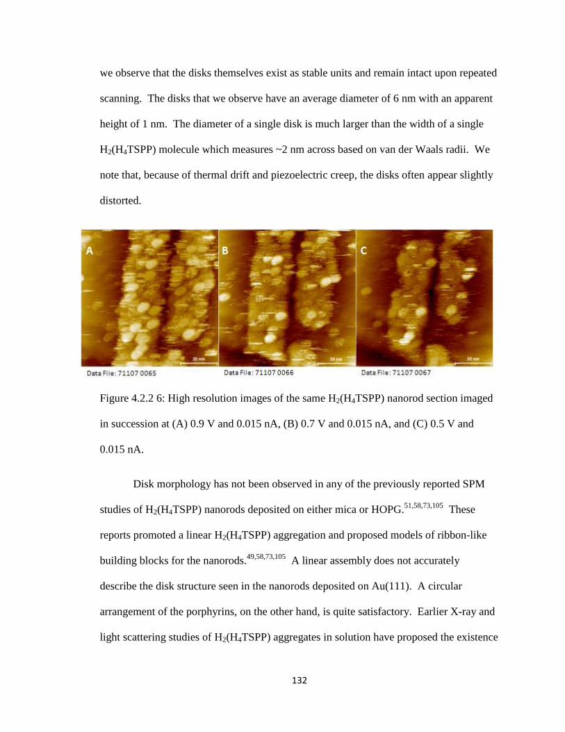
132
we observe that the disks themselves exist as stable units and remain intact upon repeated
scanning. The disks that we observe have an average diameter of 6 nm with an apparent
height of 1 nm. The diameter of a single disk is much larger than the width of a single
H2(H4TSPP) molecule which measures ~2 nm across based on van der Waals radii. We
note that, because of thermal drift and piezoelectric creep, the disks often appear slightly
distorted.
Figure 4.2.2 6: High resolution images of the same H2(H4TSPP) nanorod section imaged
in succession at (A) 0.9 V and 0.015 nA, (B) 0.7 V and 0.015 nA, and (C) 0.5 V and
0.015 nA.
Disk morphology has not been observed in any of the previously reported SPM
studies of H2(H4TSPP) nanorods deposited on either mica or HOPG.51,58,73,105
These
reports promoted a linear H2(H4TSPP) aggregation and proposed models of ribbon-like
building blocks for the nanorods.49,58,73,105
A linear assembly does not accurately
describe the disk structure seen in the nanorods deposited on Au(111). A circular
arrangement of the porphyrins, on the other hand, is quite satisfactory. Earlier X-ray and
light scattering studies of H2(H4TSPP) aggregates in solution have proposed the existence
133
of ring-like structures. Small angle X-ray scattering (SAXS) analysis suggested a
winding spiral or a series of rings forming a hollow tube measuring 16.0 nm across and 2
nm thick composed of ~26 TSPP monomers.71
A combination of elastic (ELS) and
dynamic (DLS) light scattering techniques was used to detect the presence of hierarchical
H2(H4TSPP) structures in solution: large (1-1.5 μm), medium (100-200 nm), and small
(3-6 nm) sized aggregates were reported.63,103
An aggregation number ranging between 6
and 32 was calculated for the smaller components, whereas a range of 105 to 106 was
found in the case of the large clusters.63
Ab intio calculations using optimized
H2(H4TSPP) geometry predicted a closed loop aggregate structure composed of 60-70
porphyrin monomers.157
The circular arrangement of H2(H4TSPP) molecules not only
explains the structure of the disks and the nanorods they apparently makeup but also
provides insight into their electronic behavior.
The model that we tentatively propose is a circular assembly of the H2(H4TSPP)
monomers depicted in Figure 4.2.2 7. This model is similar to the crystal structures of
circular aggregates of bacteriochlorophyll molecules (BChls B850) found in the light
harvesting systems (LH1 and LH2) of photosynthetic bacteria.15,158,159
The LH2 complex
in Rhodospirillum molischianum adopts a highly symmetrical hollow ring shape with a
radius of about 7 nm composed of 18 overlapping chlorophyll monomers.15
The internal
radius of the B850 ring is about 3.1 nm. The circular arrangement is dictated by the
noncovalent interactions between the chlorophylls (<0.35 nm) and their surrounding
protein environment. In our 6 nm H2(H4TSPP) disk model, we offer that the zwitterionic
porphyrins are arranged in a side by-side fashion stabilized by electrostatic interactions
134
between the negative sulfonate groups and the protonated pyrrole nitrogen atoms and π-π
interactions between overlapping phenyl rings. Furthermore, we do not expect the
porphyrins to be planar. X-ray diffraction studies of a protonated tetraphenyl porphine
analog, H2TPP, indicate a puckered macrocycle with pyrrole rings tilted by 28° to 33° to
minimize free energy.160
The phenyl rings are twisted by 35° allowing for a greater
conjugation with the macrocycle.160
Thus, near-planar geometry of the phenyls in the
H2(H4TSPP) monomer would favor aggregation because the charged groups on the
monomers can get close enough to interact while puckering of the porphyrin macrocycle
would induce curvature in the H2(H4TSPP) aggregate.157,161
The formation of a
symmetrical circular aggregate of N nonplanar molecules is illustrated in Figure 4.2.2 7,
where the nonplanar porphyrin is represented by a one-dimensional shape, which deviates
from linearity by the angle R. A closed ring of N molecules results when this angle
equals 2π/(N + 1). To our knowledge, the molecular structure of the diacid of
H2(H4TSPP) is not available, however, the structures of the diacid of
tetraphenylporphyrin, H2TPP2+
, in the presence of different halide counterions has been
explored.161
It was found there that the meso-substituted phenyl rings are rotated 21-33°
from the mean porphyrin plane, and the pyrrole rings adopt a saddled configuration in
which alternate rings are tilted up and down by 28-33° from the mean porphyrin plane.
Nonplanarities in this range are consistent with the formation of closed rings containing
10 to 16 porphyrins. For illustration purposes, we consider the case N = 16 (α = 21.2°)
here, taking the width of the porphyrin to be 2L = 2.2 nm based on van der Waals radii.
The porphyrins are arranged around the ring of radius R such that the positively charged
centers, represented by open circles in the figure, overlap with the negatively charged
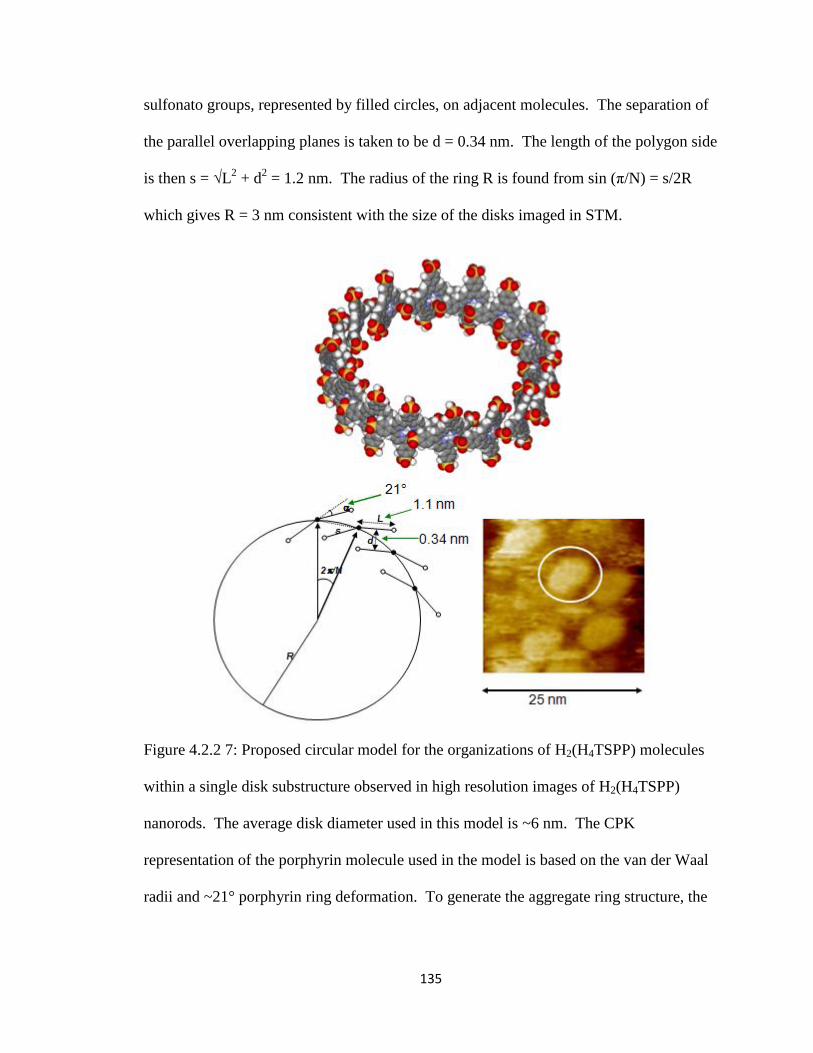
135
sulfonato groups, represented by filled circles, on adjacent molecules. The separation of
the parallel overlapping planes is taken to be d = 0.34 nm. The length of the polygon side
is then s = √L2 + d
2 = 1.2 nm. The radius of the ring R is found from sin (π/N) = s/2R
which gives R = 3 nm consistent with the size of the disks imaged in STM.
Figure 4.2.2 7: Proposed circular model for the organizations of H2(H4TSPP) molecules
within a single disk substructure observed in high resolution images of H2(H4TSPP)
nanorods. The average disk diameter used in this model is ~6 nm. The CPK
representation of the porphyrin molecule used in the model is based on the van der Waal
radii and ~21° porphyrin ring deformation. To generate the aggregate ring structure, the
136
molecules were manipulated and displayed in DS Viewer Pro (Accelrys). A 25 nm2 STM
section of the high resolution image in Figure 4.2.2.6 is inserted for reference. Below the
H2(H4TSPP) model is a schematic illustration showing a portion of a circular aggregate
containing N monomers, which deviate from planarity by R = 2π/(N + 1). Explanation of
the model is provided in the text.
We noted earlier that scanning under positive sample bias yielded clear STM
images of the nanorods. With reverse bias, it was difficult to obtain well-resolved
topography. This type of behavior is indicative of primarily LUMO mediated tunneling
associated with transient reduction (related to electron affinity) of the adsorbate.128,162
Tightly coupled LUMOs of close-packed H2(H4TSPP) were also thought responsible for
the photoconductive behavior of the nanorods upon illumination with 488 nm light
source.49
We can argue that the value of +1.3 V bias at which we obtained our best
images may be related to tunneling into delocalized π* system of the H2(H4TSPP)
monomers forming the ring structure. By taking the work function of Au(111) in air to
be 4.8 eV,163
the electron affinity of the H2(H4TSPP) aggregates is then 4.8 V - 1.3 V =
3.5 eV. This number is very close to the value measured for the reversible reduction of
H2(H4TSPP) J-aggregates deposited as films on ITO substrates and measured in
acetonitrile with TMAP as the supporting electrolyte.65
The E1/2(SCE) peak reported at -
0.84 V can be easily converted to vacuum state reference by adding 4.71 + E1/2(SCE),
resulting in a value of 3.87 V.162
The same study also reported that the reversible
reduction of the monomeric porphyrin occurred at E1/2 referenced to vacuum at 4.18 V.
The observed decrease in the reduction potential of the thin films of the H2(H4TSPP) J-
137
aggregate was postulated to result from the delocalization of electrons between the
monomer porphyrin units in the aggregate.85
The electrochemical oxidation of the
H2(H4TSPP) J-aggregate as well as the monomeric porphyrin in solution was found to be
irreversible.65
This may account for our unsatisfactory attempts to image the
H2(H4TSPP) nanorods in the negative bias. It is gratifying that the reported
electrochemical results are consistent with our STM findings. The electronic structure of
the H2(H4TSPP) aggregate will be discussed in detail in section 4.5.3.
While the proposed circular porphyrin assembly accounts well for the general
shape of the H2(H4TSPP) disks observed in our STM images, it does not account for the
lack of a more detailed structure within the disks themselves and particularly why the
disks have no cavities as our model in Figure 4.2.2 7 suggests. One possibility is that we
are tunneling into one giant delocalized π* system of the noncovalently coupled
H2(H4TSPP) circular aggregate. Interestingly, STM images of molecules composed of 24
covalently linked Zn porphyrins (C24ZB) deposited on Cu(100) appear as discrete
elongated doughnut-like shapes ~7 nm in diameter with a clearly visible hollow.164
Thus,
we tend to discount this explanation. On the other hand, the SAXS data which suggested
a winding spiral or a series of rings forming a hollow tube composed of H2(H4TSPP)
monomers showed a region of electron density in the middle of the ring that could not be
identified.71
It is possible that the electronic conductivity of the central region of the
H2(H4TSPP) disks is due to coordinated water molecules and counterions. TG and DSC
analysis shows that H2(H4TSPP) aggregates deposited on substrates release water up to
400°C indicating strongly bound water.90
These observations are also consistent with the
138
fact that the apparent height of the nanorods is the same in AFM and STM. A significant
ionic conductivity through the nanorods would explain the large conductivity necessary
for the metal-like imaging. We have identified and proposed a possible structure for the
building blocks that make up the H2(H4TSPP) nanorods. We speculate that the disks may
organize themselves into what others have termed as “ribbon-like” stacked assemblies,
which in turn group together to make up the bodies of the rods. It is also possible that the
disks may self-assemble into helical superstructures or hollow nanotubes in solution.
These nanotubes become flattened and appear as nanorods on a solid surface upon
dehydration. The adhesive forces generated by the thin film of surface water (surface
tension) may also cause collapse of tubes to rods as the solvent layer evaporates. The
absence of the stabilizing aqueous media may render the solid state rods or tubes brittle,
and they disintegrate easily with repeated probing by the STM tip making the exploration
of the mesoscopic structure of the H2(H4TSPP) nanorods difficult. The self-limiting
dimensions of the widths (20-40 nm) and heights (4 nm) of the nanorods deposited on
Au(111) and other solid substrates are intriguing and require further investigation.
For all of its strengths there are issues with the disk model. Exciton theory at its
simplest level predicts that the red-shifted 490 nm band of a circular aggregate derives
from the transition to the doubly degenerate (k = 1) excitonic states, while the blue-
shifted 424 nm band should derive from transitions to the k = 0 exciton.165
Our
depolarization ratios for 490 nm band excitation, however, are consistent with resonance
with a nondegenerate excited state (vide infra). We also note that the standard staircase
model for the aggregate is incapable of accounting for the apparent Soret band splitting,
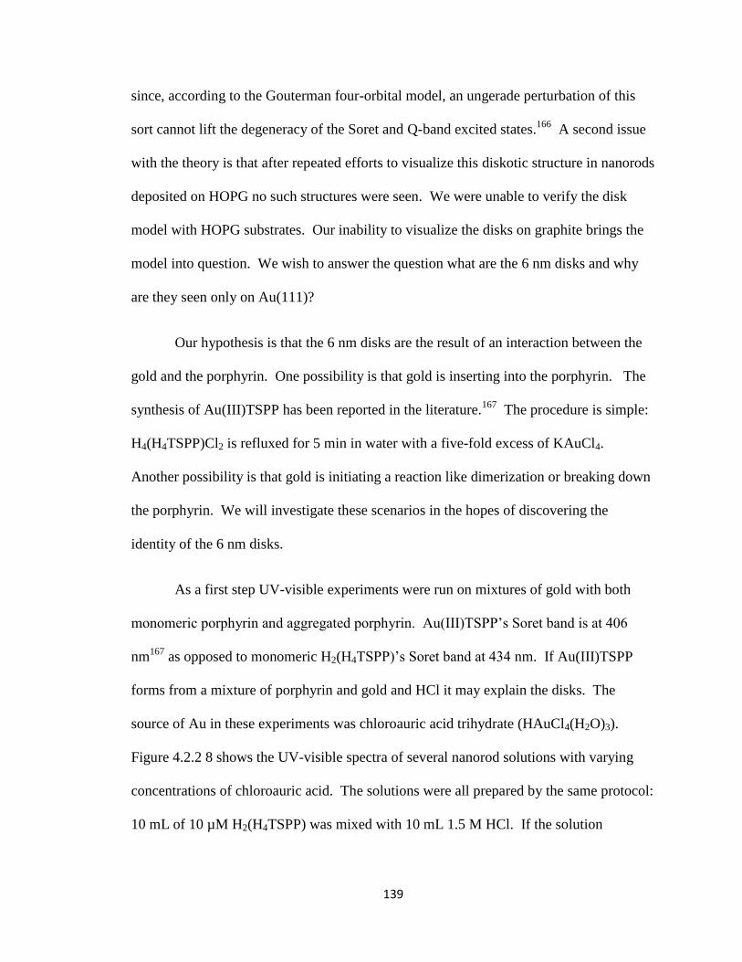
139
since, according to the Gouterman four-orbital model, an ungerade perturbation of this
sort cannot lift the degeneracy of the Soret and Q-band excited states.166
A second issue
with the theory is that after repeated efforts to visualize this diskotic structure in nanorods
deposited on HOPG no such structures were seen. We were unable to verify the disk
model with HOPG substrates. Our inability to visualize the disks on graphite brings the
model into question. We wish to answer the question what are the 6 nm disks and why
are they seen only on Au(111)?
Our hypothesis is that the 6 nm disks are the result of an interaction between the
gold and the porphyrin. One possibility is that gold is inserting into the porphyrin. The
synthesis of Au(III)TSPP has been reported in the literature.167
The procedure is simple:
H4(H4TSPP)Cl2 is refluxed for 5 min in water with a five-fold excess of KAuCl4.
Another possibility is that gold is initiating a reaction like dimerization or breaking down
the porphyrin. We will investigate these scenarios in the hopes of discovering the
identity of the 6 nm disks.
As a first step UV-visible experiments were run on mixtures of gold with both
monomeric porphyrin and aggregated porphyrin. Au(III)TSPP‟s Soret band is at 406
nm167
as opposed to monomeric H2(H4TSPP)‟s Soret band at 434 nm. If Au(III)TSPP
forms from a mixture of porphyrin and gold and HCl it may explain the disks. The
source of Au in these experiments was chloroauric acid trihydrate (HAuCl4(H2O)3).
Figure 4.2.2 8 shows the UV-visible spectra of several nanorod solutions with varying
concentrations of chloroauric acid. The solutions were all prepared by the same protocol:
10 mL of 10 µM H2(H4TSPP) was mixed with 10 mL 1.5 M HCl. If the solution
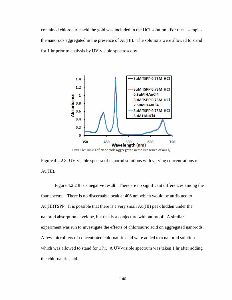
140
contained chloroauric acid the gold was included in the HCl solution. For these samples
the nanorods aggregated in the presence of Au(III). The solutions were allowed to stand
for 1 hr prior to analysis by UV-visible spectroscopy.
Figure 4.2.2 8: UV-visible spectra of nanorod solutions with varying concentrations of
Au(III).
Figure 4.2.2 8 is a negative result. There are no significant differences among the
four spectra. There is no discernable peak at 406 nm which would be attributed to
Au(III)TSPP. It is possible that there is a very small Au(III) peak hidden under the
nanorod absorption envelope, but that is a conjecture without proof. A similar
experiment was run to investigate the effects of chloroauric acid on aggregated nanorods.
A few microliters of concentrated chloroauric acid were added to a nanorod solution
which was allowed to stand for 1 hr. A UV-visible spectrum was taken 1 hr after adding
the chloroauric acid.
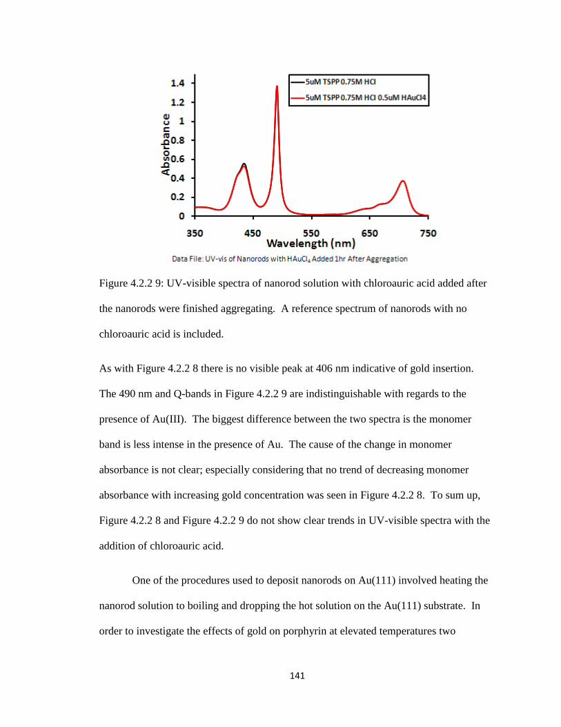
141
Figure 4.2.2 9: UV-visible spectra of nanorod solution with chloroauric acid added after
the nanorods were finished aggregating. A reference spectrum of nanorods with no
chloroauric acid is included.
As with Figure 4.2.2 8 there is no visible peak at 406 nm indicative of gold insertion.
The 490 nm and Q-bands in Figure 4.2.2 9 are indistinguishable with regards to the
presence of Au(III). The biggest difference between the two spectra is the monomer
band is less intense in the presence of Au. The cause of the change in monomer
absorbance is not clear; especially considering that no trend of decreasing monomer
absorbance with increasing gold concentration was seen in Figure 4.2.2 8. To sum up,
Figure 4.2.2 8 and Figure 4.2.2 9 do not show clear trends in UV-visible spectra with the
addition of chloroauric acid.
One of the procedures used to deposit nanorods on Au(111) involved heating the
nanorod solution to boiling and dropping the hot solution on the Au(111) substrate. In
order to investigate the effects of gold on porphyrin at elevated temperatures two
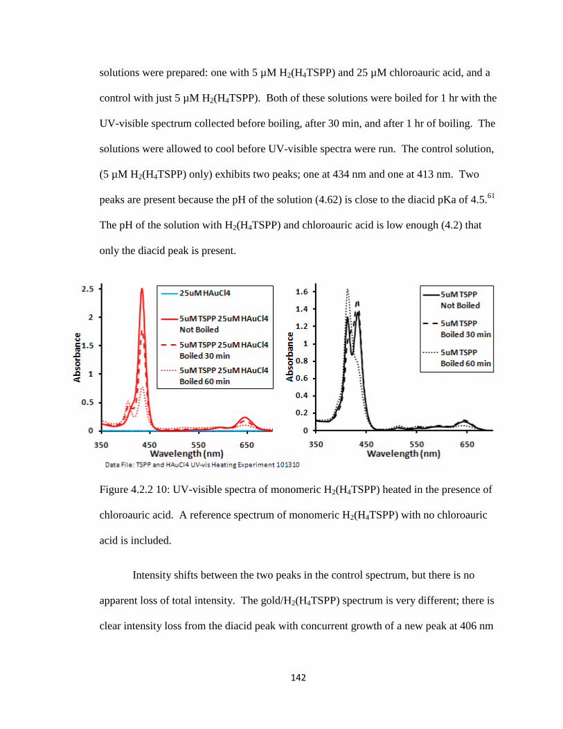
142
solutions were prepared: one with 5 µM H2(H4TSPP) and 25 µM chloroauric acid, and a
control with just 5 µM H2(H4TSPP). Both of these solutions were boiled for 1 hr with the
UV-visible spectrum collected before boiling, after 30 min, and after 1 hr of boiling. The
solutions were allowed to cool before UV-visible spectra were run. The control solution,
(5 µM H2(H4TSPP) only) exhibits two peaks; one at 434 nm and one at 413 nm. Two
peaks are present because the pH of the solution (4.62) is close to the diacid pKa of 4.5.61
The pH of the solution with H2(H4TSPP) and chloroauric acid is low enough (4.2) that
only the diacid peak is present.
Figure 4.2.2 10: UV-visible spectra of monomeric H2(H4TSPP) heated in the presence of
chloroauric acid. A reference spectrum of monomeric H2(H4TSPP) with no chloroauric
acid is included.
Intensity shifts between the two peaks in the control spectrum, but there is no
apparent loss of total intensity. The gold/H2(H4TSPP) spectrum is very different; there is
clear intensity loss from the diacid peak with concurrent growth of a new peak at 406 nm
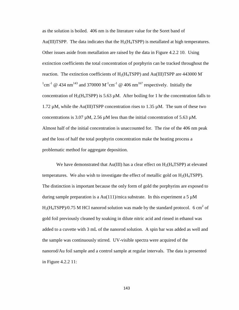
143
as the solution is boiled. 406 nm is the literature value for the Soret band of
Au(III)TSPP. The data indicates that the H2(H4TSPP) is metallated at high temperatures.
Other issues aside from metallation are raised by the data in Figure 4.2.2 10. Using
extinction coefficients the total concentration of porphyrin can be tracked throughout the
reaction. The extinction coefficients of H2(H4TSPP) and Au(III)TSPP are 443000 M-
1cm
-1 @ 434 nm
143 and 370000 M
-1cm
-1 @ 406 nm
167 respectively. Initially the
concentration of H2(H4TSPP) is 5.63 µM. After boiling for 1 hr the concentration falls to
1.72 µM, while the Au(III)TSPP concentration rises to 1.35 µM. The sum of these two
concentrations is 3.07 µM, 2.56 µM less than the initial concentration of 5.63 µM.
Almost half of the initial concentration is unaccounted for. The rise of the 406 nm peak
and the loss of half the total porphyrin concentration make the heating process a
problematic method for aggregate deposition.
We have demonstrated that Au(III) has a clear effect on H2(H4TSPP) at elevated
temperatures. We also wish to investigate the effect of metallic gold on H2(H4TSPP).
The distinction is important because the only form of gold the porphyrins are exposed to
during sample preparation is a Au(111)/mica substrate. In this experiment a 5 µM
H2(H4TSPP)/0.75 M HCl nanorod solution was made by the standard protocol. 6 cm2 of
gold foil previously cleaned by soaking in dilute nitric acid and rinsed in ethanol was
added to a cuvette with 3 mL of the nanorod solution. A spin bar was added as well and
the sample was continuously stirred. UV-visible spectra were acquired of the
nanorod/Au foil sample and a control sample at regular intervals. The data is presented
in Figure 4.2.2 11:
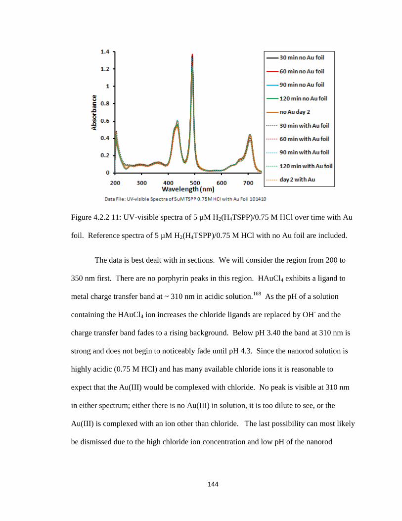
144
Figure 4.2.2 11: UV-visible spectra of 5 µM H2(H4TSPP)/0.75 M HCl over time with Au
foil. Reference spectra of 5 µM H2(H4TSPP)/0.75 M HCl with no Au foil are included.
The data is best dealt with in sections. We will consider the region from 200 to
350 nm first. There are no porphyrin peaks in this region. HAuCl4 exhibits a ligand to
metal charge transfer band at ~ 310 nm in acidic solution.168
As the pH of a solution
containing the HAuCl4 ion increases the chloride ligands are replaced by OH- and the
charge transfer band fades to a rising background. Below pH 3.40 the band at 310 nm is
strong and does not begin to noticeably fade until pH 4.3. Since the nanorod solution is
highly acidic (0.75 M HCl) and has many available chloride ions it is reasonable to
expect that the Au(III) would be complexed with chloride. No peak is visible at 310 nm
in either spectrum; either there is no Au(III) in solution, it is too dilute to see, or the
Au(III) is complexed with an ion other than chloride. The last possibility can most likely
be dismissed due to the high chloride ion concentration and low pH of the nanorod
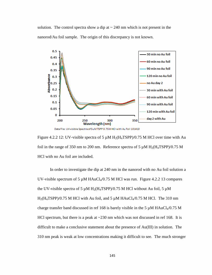
145
solution. The control spectra show a dip at ~ 240 nm which is not present in the
nanorod/Au foil sample. The origin of this discrepancy is not known.
Figure 4.2.2 12: UV-visible spectra of 5 µM H2(H4TSPP)/0.75 M HCl over time with Au
foil in the range of 350 nm to 200 nm. Reference spectra of 5 µM H2(H4TSPP)/0.75 M
HCl with no Au foil are included.
In order to investigate the dip at 240 nm in the nanorod with no Au foil solution a
UV-visible spectrum of 5 µM HAuCl4/0.75 M HCl was run. Figure 4.2.2 13 compares
the UV-visible spectra of 5 µM H2(H4TSPP)/0.75 M HCl without Au foil, 5 µM
H2(H4TSPP)/0.75 M HCl with Au foil, and 5 µM HAuCl4/0.75 M HCl. The 310 nm
charge transfer band discussed in ref 168 is barely visible in the 5 µM HAuCl4/0.75 M
HCl spectrum, but there is a peak at ~230 nm which was not discussed in ref 168. It is
difficult to make a conclusive statement about the presence of Au(III) in solution. The
310 nm peak is weak at low concentrations making it difficult to see. The much stronger
146
peak at 230 nm does not fit exactly in the dip at 240 nm in the gold free nanorod solution
spectrum. In summary, based on Figure 4.2.2 12 and Figure 4.2.2 13 we cannot confirm
the presence of Au(III) in solution. We cannot rule it out at small concentrations either.
Figure 4.2.2 13: UV-visible spectra of 5 µM H2(H4TSPP)/0.75 M HCl with Au foil and 5
µM HAuCl4/0.75 M HCl in the range of 350 nm to 200 nm. A reference spectrum of 5
µM H2(H4TSPP)/0.75 M HCl with no Au foil is included.
Analysis of the Q-band region is straightforward. In all cases the spectra with Au
foil are lower than the control spectra. Interestingly, the control spectra are constant
while the spectra with Au foil drop markedly from the 30 min spectrum to the 60 min
spectrum. The reason for the difference is not clear from the UV-visible data. The
aggregate responsible for the 707 nm band may be depositing on the Au foil, or the
porphyrin is being broken down in a similar fashion as Figure 4.2.2 10.
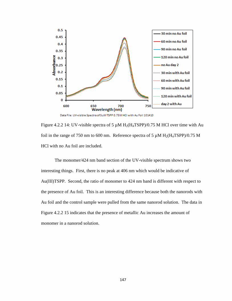
147
Figure 4.2.2 14: UV-visible spectra of 5 µM H2(H4TSPP)/0.75 M HCl over time with Au
foil in the range of 750 nm to 600 nm. Reference spectra of 5 µM H2(H4TSPP)/0.75 M
HCl with no Au foil are included.
The monomer/424 nm band section of the UV-visible spectrum shows two
interesting things. First, there is no peak at 406 nm which would be indicative of
Au(III)TSPP. Second, the ratio of monomer to 424 nm band is different with respect to
the presence of Au foil. This is an interesting difference because both the nanorods with
Au foil and the control sample were pulled from the same nanorod solution. The data in
Figure 4.2.2 15 indicates that the presence of metallic Au increases the amount of
monomer in a nanorod solution.
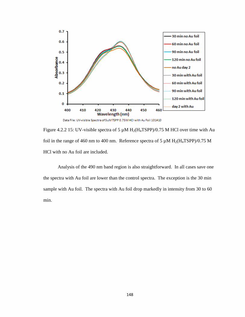
148
Figure 4.2.2 15: UV-visible spectra of 5 µM H2(H4TSPP)/0.75 M HCl over time with Au
foil in the range of 460 nm to 400 nm. Reference spectra of 5 µM H2(H4TSPP)/0.75 M
HCl with no Au foil are included.
Analysis of the 490 nm band region is also straightforward. In all cases save one
the spectra with Au foil are lower than the control spectra. The exception is the 30 min
sample with Au foil. The spectra with Au foil drop markedly in intensity from 30 to 60
min.
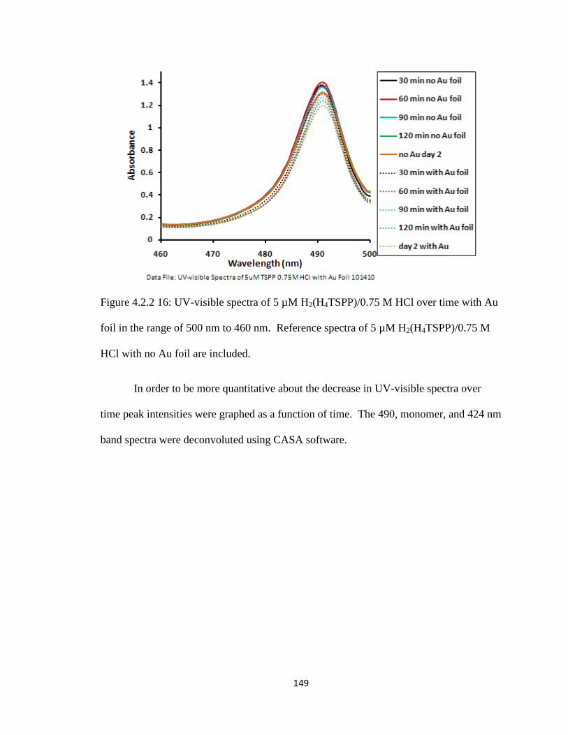
149
Figure 4.2.2 16: UV-visible spectra of 5 µM H2(H4TSPP)/0.75 M HCl over time with Au
foil in the range of 500 nm to 460 nm. Reference spectra of 5 µM H2(H4TSPP)/0.75 M
HCl with no Au foil are included.
In order to be more quantitative about the decrease in UV-visible spectra over
time peak intensities were graphed as a function of time. The 490, monomer, and 424 nm
band spectra were deconvoluted using CASA software.
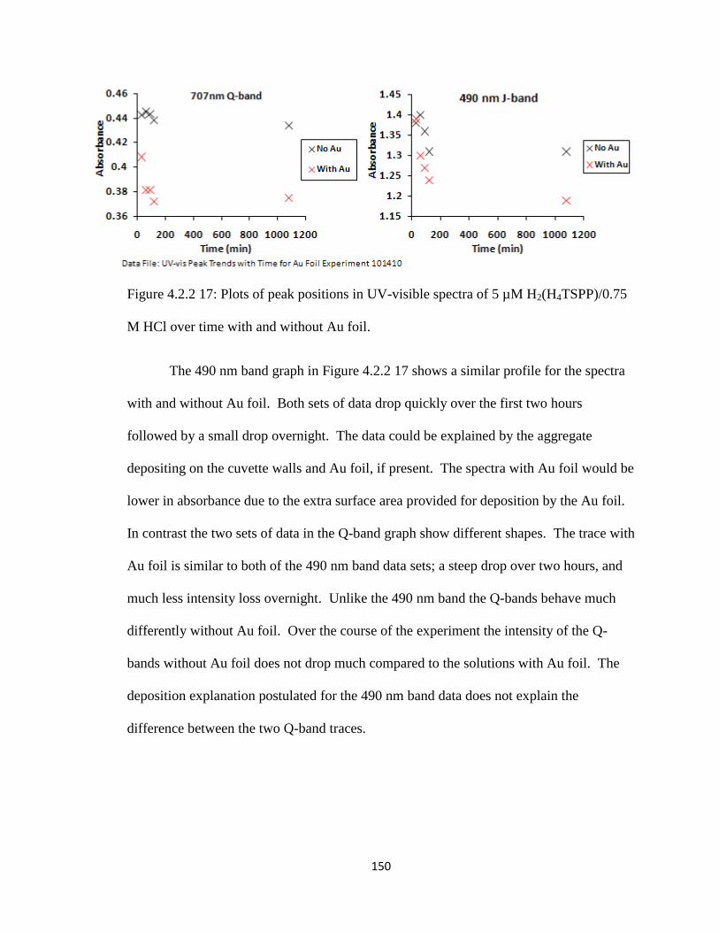
150
Figure 4.2.2 17: Plots of peak positions in UV-visible spectra of 5 µM H2(H4TSPP)/0.75
M HCl over time with and without Au foil.
The 490 nm band graph in Figure 4.2.2 17 shows a similar profile for the spectra
with and without Au foil. Both sets of data drop quickly over the first two hours
followed by a small drop overnight. The data could be explained by the aggregate
depositing on the cuvette walls and Au foil, if present. The spectra with Au foil would be
lower in absorbance due to the extra surface area provided for deposition by the Au foil.
In contrast the two sets of data in the Q-band graph show different shapes. The trace with
Au foil is similar to both of the 490 nm band data sets; a steep drop over two hours, and
much less intensity loss overnight. Unlike the 490 nm band the Q-bands behave much
differently without Au foil. Over the course of the experiment the intensity of the Q-
bands without Au foil does not drop much compared to the solutions with Au foil. The
deposition explanation postulated for the 490 nm band data does not explain the
difference between the two Q-band traces.
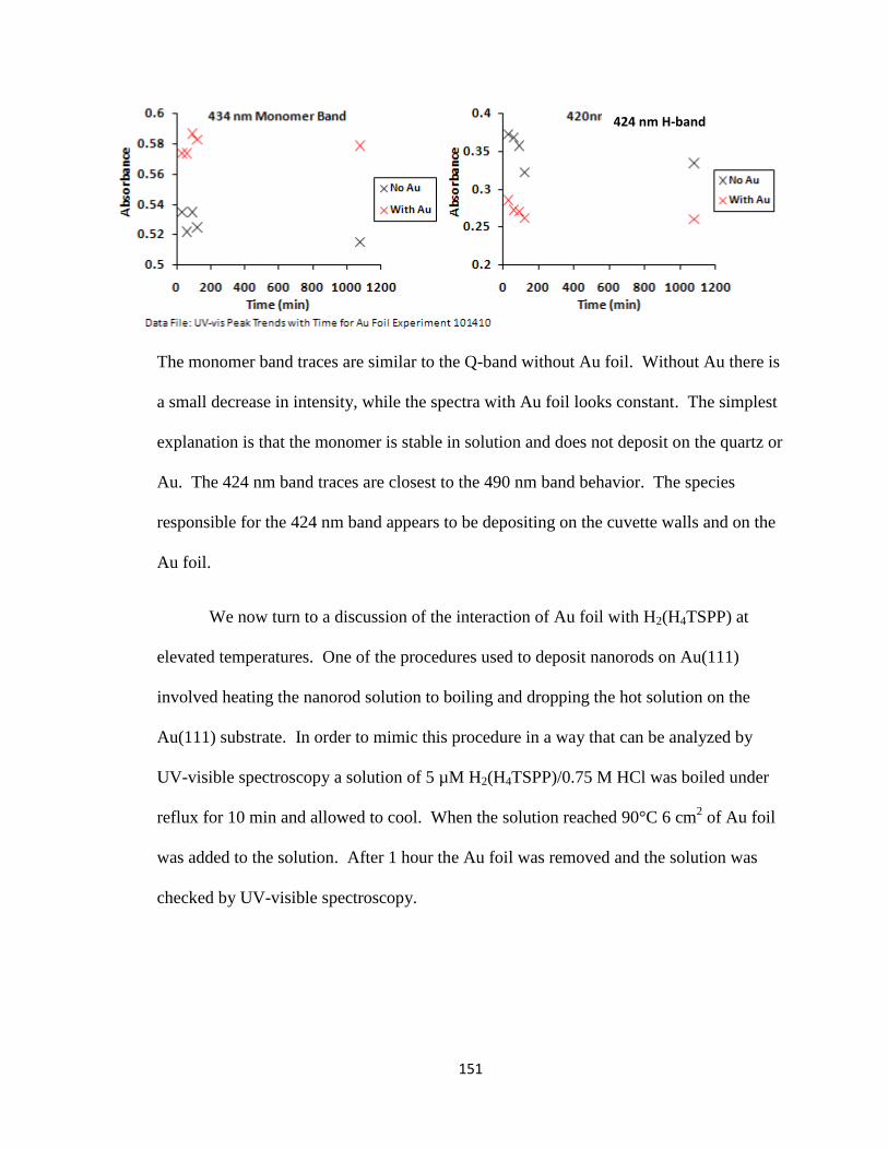
151
The monomer band traces are similar to the Q-band without Au foil. Without Au there is
a small decrease in intensity, while the spectra with Au foil looks constant. The simplest
explanation is that the monomer is stable in solution and does not deposit on the quartz or
Au. The 424 nm band traces are closest to the 490 nm band behavior. The species
responsible for the 424 nm band appears to be depositing on the cuvette walls and on the
Au foil.
We now turn to a discussion of the interaction of Au foil with H2(H4TSPP) at
elevated temperatures. One of the procedures used to deposit nanorods on Au(111)
involved heating the nanorod solution to boiling and dropping the hot solution on the
Au(111) substrate. In order to mimic this procedure in a way that can be analyzed by
UV-visible spectroscopy a solution of 5 µM H2(H4TSPP)/0.75 M HCl was boiled under
reflux for 10 min and allowed to cool. When the solution reached 90°C 6 cm2 of Au foil
was added to the solution. After 1 hour the Au foil was removed and the solution was
checked by UV-visible spectroscopy.
424 nm H-band
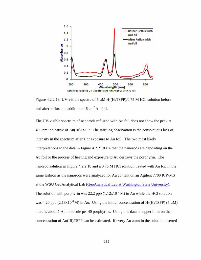
152
Figure 4.2.2 18: UV-visible spectra of 5 µM H2(H4TSPP)/0.75 M HCl solution before
and after reflux and addition of 6 cm2
Au foil.
The UV-visible spectrum of nanorods refluxed with Au foil does not show the peak at
406 nm indicative of Au(III)TSPP. The startling observation is the conspicuous loss of
intensity in the spectrum after 1 hr exposure to Au foil. The two most likely
interpretations to the data in Figure 4.2.2 18 are that the nanorods are depositing on the
Au foil or the process of heating and exposure to Au destroys the porphyrin. The
nanorod solution in Figure 4.2.2 18 and a 0.75 M HCl solution treated with Au foil in the
same fashion as the nanorods were analyzed for Au content on an Agilent 7700 ICP-MS
at the WSU GeoAnalytical Lab (GeoAnalytical Lab at Washington State University).
The solution with porphyrin was 22.2 ppb (1.12x10⁻⁷
M) in Au while the HCl solution
was 4.20 ppb (2.18x10⁻⁸
M) in Au. Using the initial concentration of H2(H4TSPP) (5 µM)
there is about 1 Au molecule per 40 porphyrins. Using this data an upper limit on the
concentration of Au(III)TSPP can be estimated. If every Au atom in the solution inserted
153
into a porphyrin the resulting absorbance at 406 nm would be 4x10⁻²
(based upon the
extinction coefficient); too low to be seen in the UV-visible spectra in Figure 4.2.2 18. It
is interesting that the porphyrin solution is much higher in Au than the HCl solution. It
may be that the porphyrin plays a part in the dissolution of the Au foil. Another
possibility is that the difference in Au concentration is indicative of the reproducibility
(or lack thereof) of the experiment. The same amount of foil was used in both
experiments, but upon addition of the foil to the hot solution it settled to the bottom of the
flask. Depending on how the foil settled at the bottom of the flask a different amount of
surface area may have been exposed to the solution, changing the rate of Au dissolution.
ICP-MS testing has confirmed the presence of Au in the refluxed nanorod solution, but at
low concentrations.
Having demonstrated the dissolution of Au into HCl solution at elevated
temperatures STM images of Au(111)/mica and HOPG substrates treated with 0.75 M
HCl (only) for the 1 hr were taken in order to explore the effects of HCl on microscopy
substrates. Figure 4.2.2 19 shows STM images of peeled HOPG and HOPG treated with
0.75 M HCl for 1 hr.
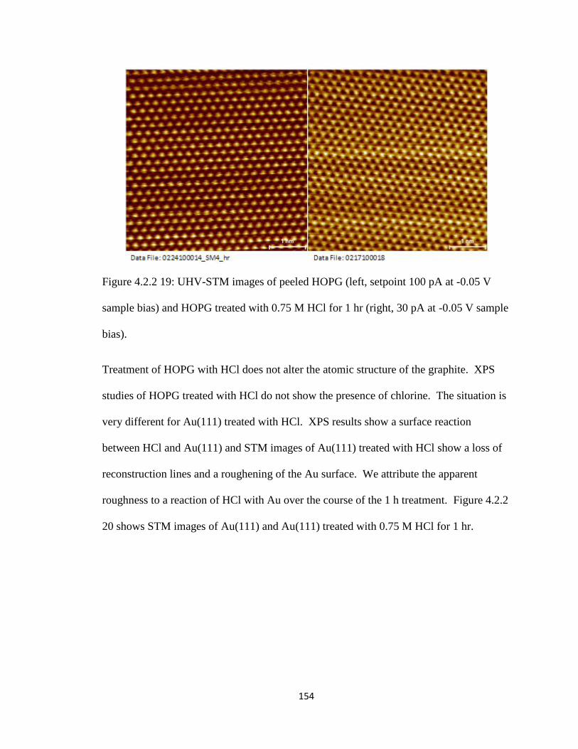
154
Figure 4.2.2 19: UHV-STM images of peeled HOPG (left, setpoint 100 pA at -0.05 V
sample bias) and HOPG treated with 0.75 M HCl for 1 hr (right, 30 pA at -0.05 V sample
bias).
Treatment of HOPG with HCl does not alter the atomic structure of the graphite. XPS
studies of HOPG treated with HCl do not show the presence of chlorine. The situation is
very different for Au(111) treated with HCl. XPS results show a surface reaction
between HCl and Au(111) and STM images of Au(111) treated with HCl show a loss of
reconstruction lines and a roughening of the Au surface. We attribute the apparent
roughness to a reaction of HCl with Au over the course of the 1 h treatment. Figure 4.2.2
20 shows STM images of Au(111) and Au(111) treated with 0.75 M HCl for 1 hr.
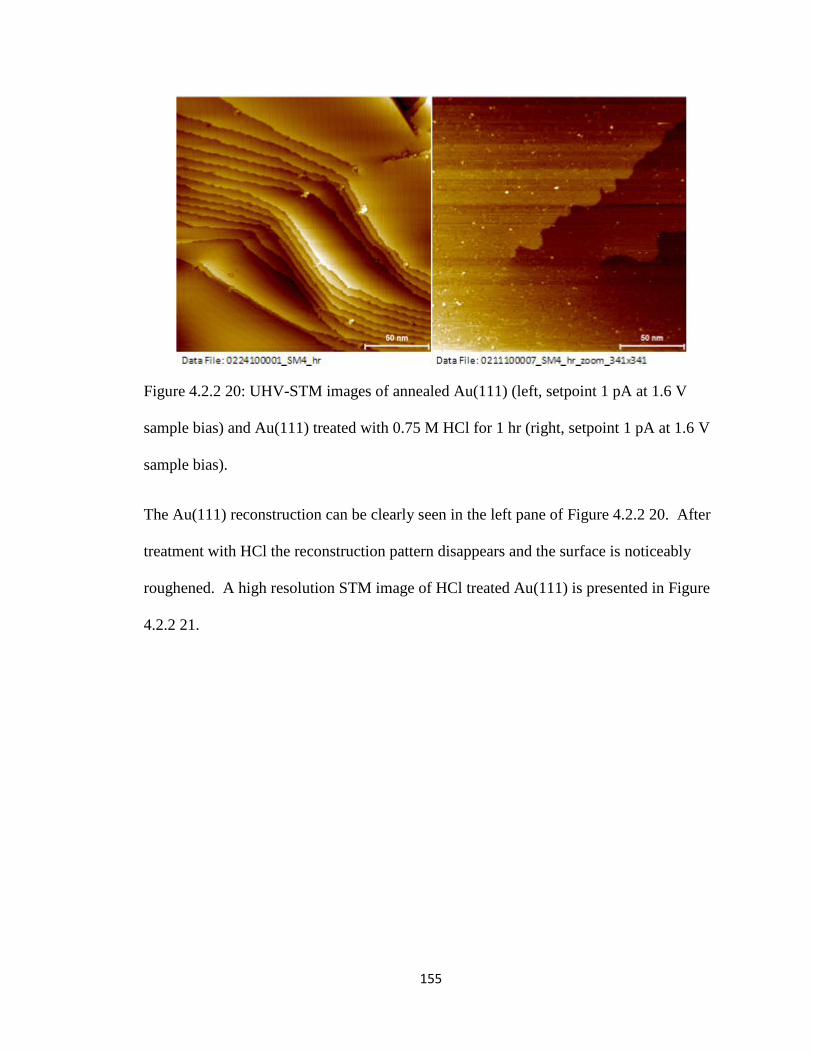
155
Figure 4.2.2 20: UHV-STM images of annealed Au(111) (left, setpoint 1 pA at 1.6 V
sample bias) and Au(111) treated with 0.75 M HCl for 1 hr (right, setpoint 1 pA at 1.6 V
sample bias).
The Au(111) reconstruction can be clearly seen in the left pane of Figure 4.2.2 20. After
treatment with HCl the reconstruction pattern disappears and the surface is noticeably
roughened. A high resolution STM image of HCl treated Au(111) is presented in Figure
4.2.2 21.
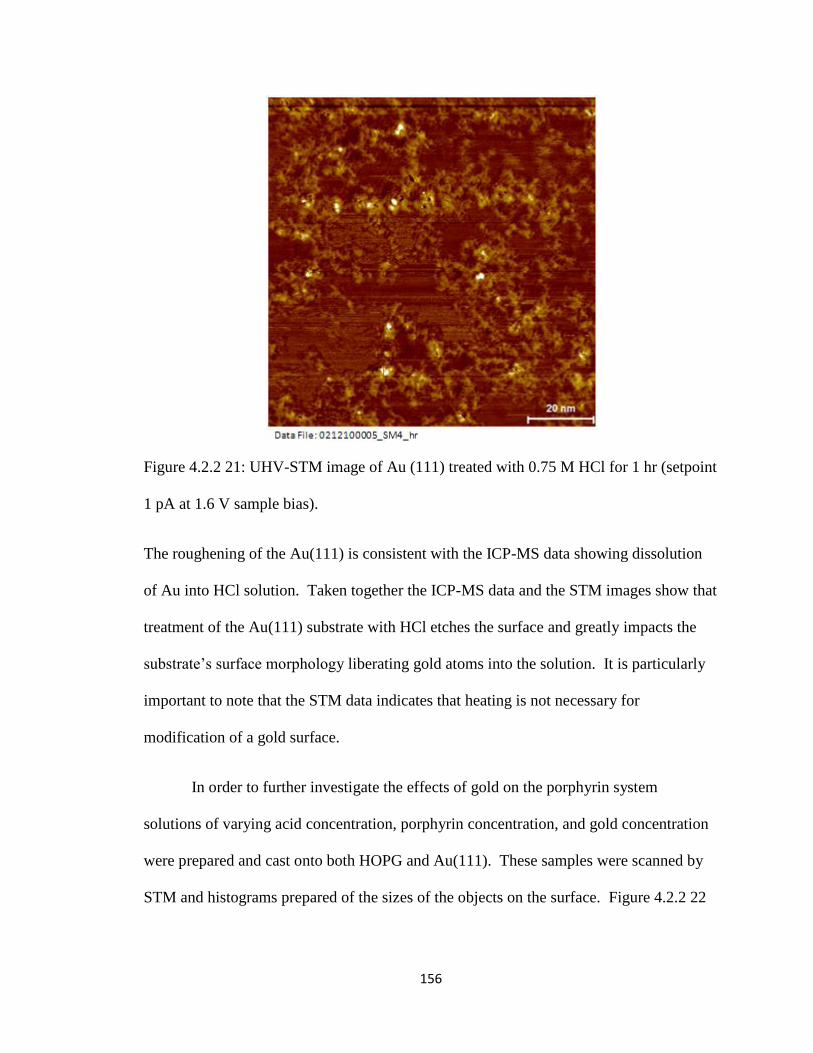
156
Figure 4.2.2 21: UHV-STM image of Au (111) treated with 0.75 M HCl for 1 hr (setpoint
1 pA at 1.6 V sample bias).
The roughening of the Au(111) is consistent with the ICP-MS data showing dissolution
of Au into HCl solution. Taken together the ICP-MS data and the STM images show that
treatment of the Au(111) substrate with HCl etches the surface and greatly impacts the
substrate‟s surface morphology liberating gold atoms into the solution. It is particularly
important to note that the STM data indicates that heating is not necessary for
modification of a gold surface.
In order to further investigate the effects of gold on the porphyrin system
solutions of varying acid concentration, porphyrin concentration, and gold concentration
were prepared and cast onto both HOPG and Au(111). These samples were scanned by
STM and histograms prepared of the sizes of the objects on the surface. Figure 4.2.2 22
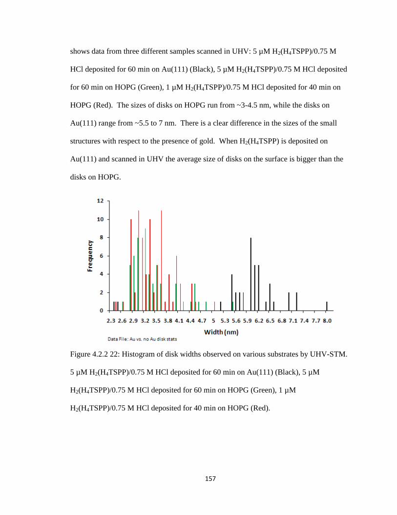
157
shows data from three different samples scanned in UHV: 5 µM H2(H4TSPP)/0.75 M
HCl deposited for 60 min on Au(111) (Black), 5 µM H2(H4TSPP)/0.75 M HCl deposited
for 60 min on HOPG (Green), 1 µM H2(H4TSPP)/0.75 M HCl deposited for 40 min on
HOPG (Red). The sizes of disks on HOPG run from ~3-4.5 nm, while the disks on
Au(111) range from ~5.5 to 7 nm. There is a clear difference in the sizes of the small
structures with respect to the presence of gold. When H2(H4TSPP) is deposited on
Au(111) and scanned in UHV the average size of disks on the surface is bigger than the
disks on HOPG.
Figure 4.2.2 22: Histogram of disk widths observed on various substrates by UHV-STM.
5 µM H2(H4TSPP)/0.75 M HCl deposited for 60 min on Au(111) (Black), 5 µM
H2(H4TSPP)/0.75 M HCl deposited for 60 min on HOPG (Green), 1 µM
H2(H4TSPP)/0.75 M HCl deposited for 40 min on HOPG (Red).
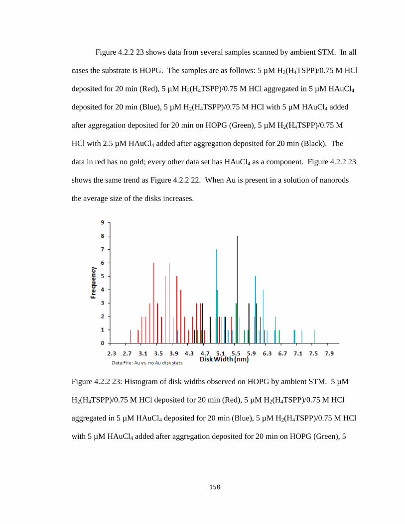
158
Figure 4.2.2 23 shows data from several samples scanned by ambient STM. In all
cases the substrate is HOPG. The samples are as follows: 5 µM H2(H4TSPP)/0.75 M HCl
deposited for 20 min (Red), 5 µM H2(H4TSPP)/0.75 M HCl aggregated in 5 µM HAuCl4
deposited for 20 min (Blue), 5 µM H2(H4TSPP)/0.75 M HCl with 5 µM HAuCl4 added
after aggregation deposited for 20 min on HOPG (Green), 5 µM H2(H4TSPP)/0.75 M
HCl with 2.5 µM HAuCl4 added after aggregation deposited for 20 min (Black). The
data in red has no gold; every other data set has HAuCl4 as a component. Figure 4.2.2 23
shows the same trend as Figure 4.2.2 22. When Au is present in a solution of nanorods
the average size of the disks increases.
Figure 4.2.2 23: Histogram of disk widths observed on HOPG by ambient STM. 5 µM
H2(H4TSPP)/0.75 M HCl deposited for 20 min (Red), 5 µM H2(H4TSPP)/0.75 M HCl
aggregated in 5 µM HAuCl4 deposited for 20 min (Blue), 5 µM H2(H4TSPP)/0.75 M HCl
with 5 µM HAuCl4 added after aggregation deposited for 20 min on HOPG (Green), 5
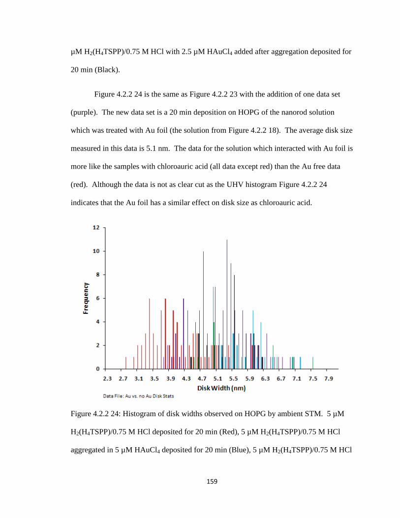
159
µM H2(H4TSPP)/0.75 M HCl with 2.5 µM HAuCl4 added after aggregation deposited for
20 min (Black).
Figure 4.2.2 24 is the same as Figure 4.2.2 23 with the addition of one data set
(purple). The new data set is a 20 min deposition on HOPG of the nanorod solution
which was treated with Au foil (the solution from Figure 4.2.2 18). The average disk size
measured in this data is 5.1 nm. The data for the solution which interacted with Au foil is
more like the samples with chloroauric acid (all data except red) than the Au free data
(red). Although the data is not as clear cut as the UHV histogram Figure 4.2.2 24
indicates that the Au foil has a similar effect on disk size as chloroauric acid.
Figure 4.2.2 24: Histogram of disk widths observed on HOPG by ambient STM. 5 µM
H2(H4TSPP)/0.75 M HCl deposited for 20 min (Red), 5 µM H2(H4TSPP)/0.75 M HCl
aggregated in 5 µM HAuCl4 deposited for 20 min (Blue), 5 µM H2(H4TSPP)/0.75 M HCl
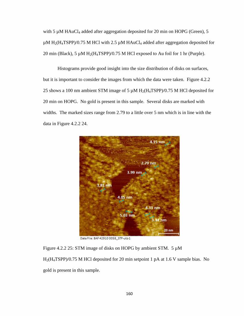
160
with 5 µM HAuCl4 added after aggregation deposited for 20 min on HOPG (Green), 5
µM H2(H4TSPP)/0.75 M HCl with 2.5 µM HAuCl4 added after aggregation deposited for
20 min (Black), 5 µM H2(H4TSPP)/0.75 M HCl exposed to Au foil for 1 hr (Purple).
Histograms provide good insight into the size distribution of disks on surfaces,
but it is important to consider the images from which the data were taken. Figure 4.2.2
25 shows a 100 nm ambient STM image of 5 µM H2(H4TSPP)/0.75 M HCl deposited for
20 min on HOPG. No gold is present in this sample. Several disks are marked with
widths. The marked sizes range from 2.79 to a little over 5 nm which is in line with the
data in Figure 4.2.2 24.
Figure 4.2.2 25: STM image of disks on HOPG by ambient STM. 5 µM
H2(H4TSPP)/0.75 M HCl deposited for 20 min setpoint 1 pA at 1.6 V sample bias. No
gold is present in this sample.
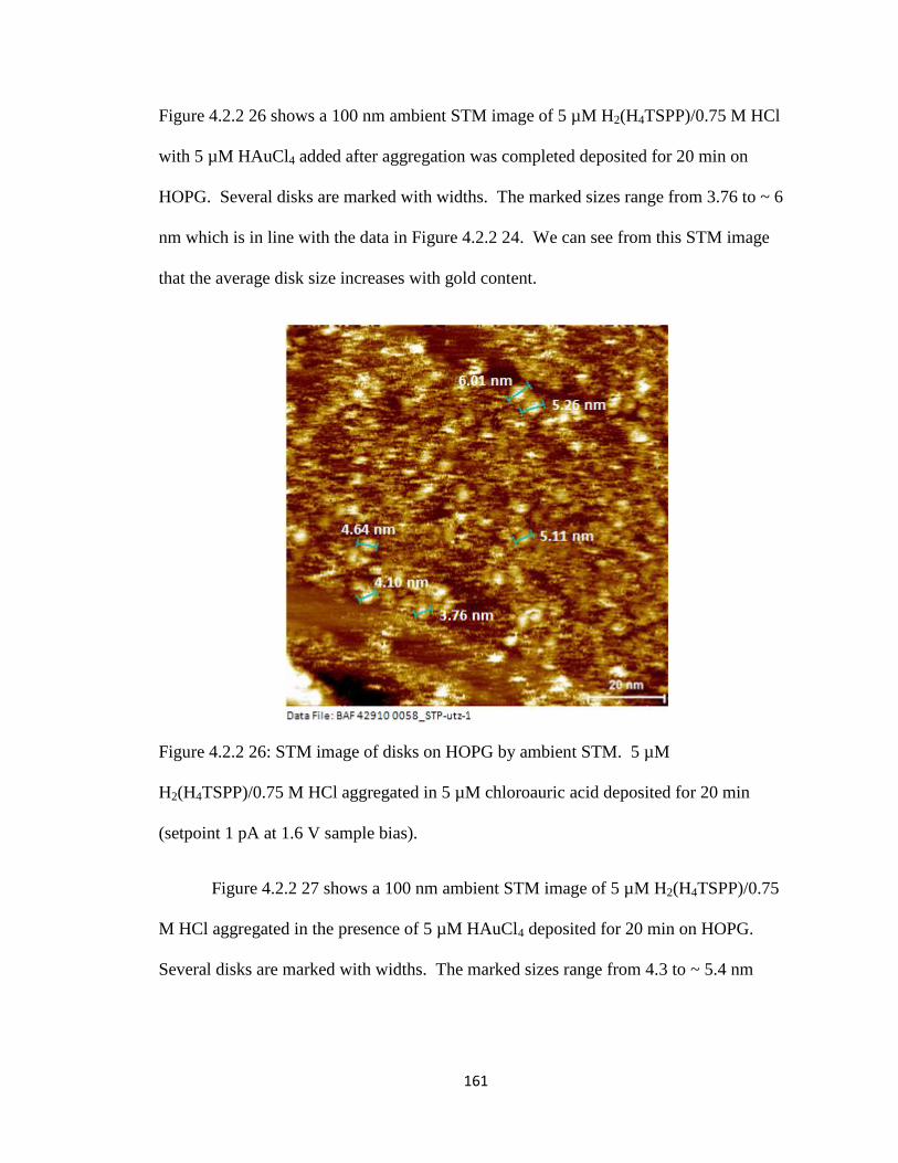
161
Figure 4.2.2 26 shows a 100 nm ambient STM image of 5 µM H2(H4TSPP)/0.75 M HCl
with 5 µM HAuCl4 added after aggregation was completed deposited for 20 min on
HOPG. Several disks are marked with widths. The marked sizes range from 3.76 to ~ 6
nm which is in line with the data in Figure 4.2.2 24. We can see from this STM image
that the average disk size increases with gold content.
Figure 4.2.2 26: STM image of disks on HOPG by ambient STM. 5 µM
H2(H4TSPP)/0.75 M HCl aggregated in 5 µM chloroauric acid deposited for 20 min
(setpoint 1 pA at 1.6 V sample bias).
Figure 4.2.2 27 shows a 100 nm ambient STM image of 5 µM H2(H4TSPP)/0.75
M HCl aggregated in the presence of 5 µM HAuCl4 deposited for 20 min on HOPG.
Several disks are marked with widths. The marked sizes range from 4.3 to ~ 5.4 nm
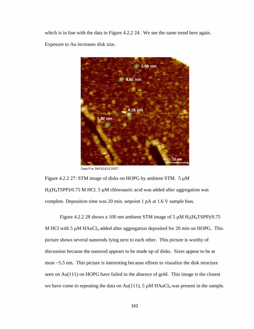
162
which is in line with the data in Figure 4.2.2 24. We see the same trend here again.
Exposure to Au increases disk size.
Figure 4.2.2 27: STM image of disks on HOPG by ambient STM. 5 µM
H2(H4TSPP)/0.75 M HCl. 5 µM chloroauric acid was added after aggregation was
complete. Deposition time was 20 min. setpoint 1 pA at 1.6 V sample bias.
Figure 4.2.2 28 shows a 100 nm ambient STM image of 5 µM H2(H4TSPP)/0.75
M HCl with 5 µM HAuCl4 added after aggregation deposited for 20 min on HOPG. This
picture shows several nanorods lying next to each other. This picture is worthy of
discussion because the nanorod appears to be made up of disks. Sizes appear to be at
most ~5.5 nm. This picture is interesting because efforts to visualize the disk structure
seen on Au(111) on HOPG have failed in the absence of gold. This image is the closest
we have come to repeating the data on Au(111), 5 µM HAuCl4 was present in the sample.
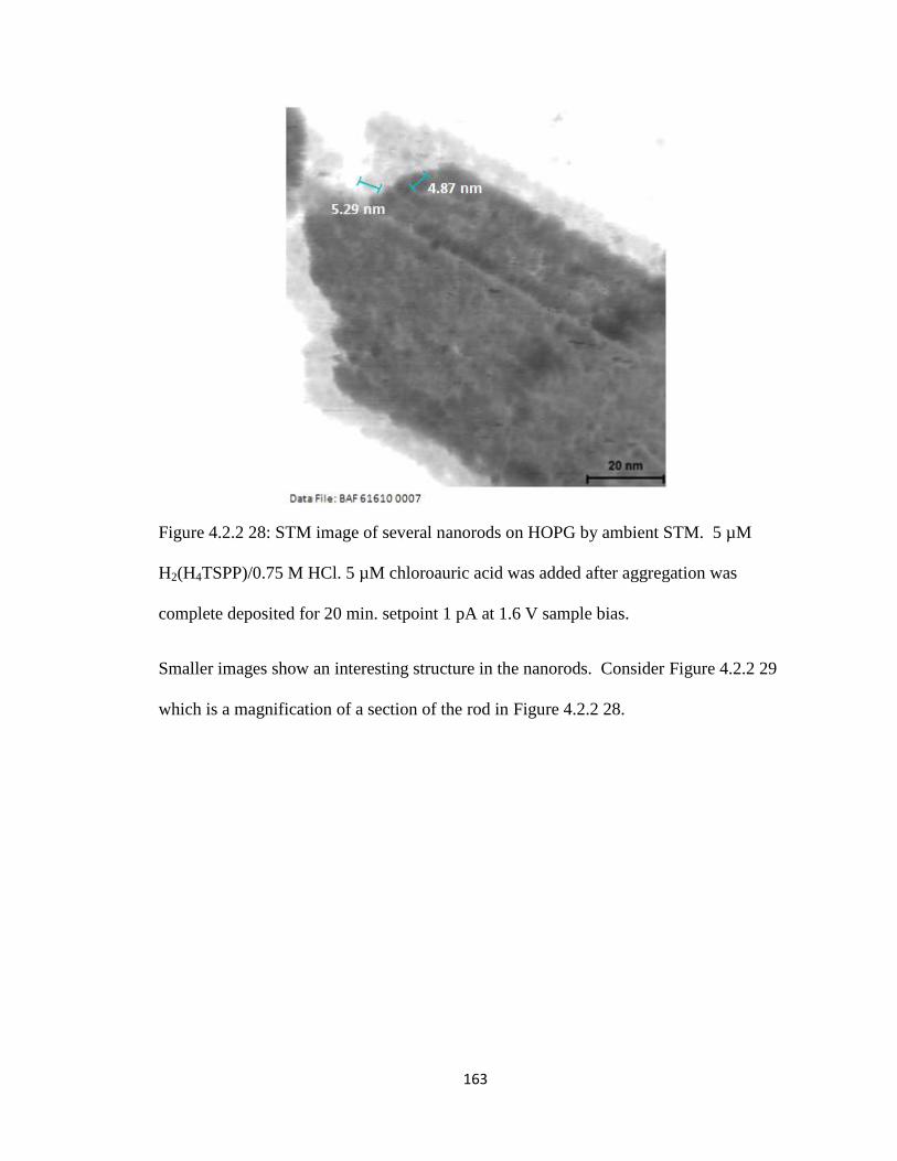
163
Figure 4.2.2 28: STM image of several nanorods on HOPG by ambient STM. 5 µM
H2(H4TSPP)/0.75 M HCl. 5 µM chloroauric acid was added after aggregation was
complete deposited for 20 min. setpoint 1 pA at 1.6 V sample bias.
Smaller images show an interesting structure in the nanorods. Consider Figure 4.2.2 29
which is a magnification of a section of the rod in Figure 4.2.2 28.
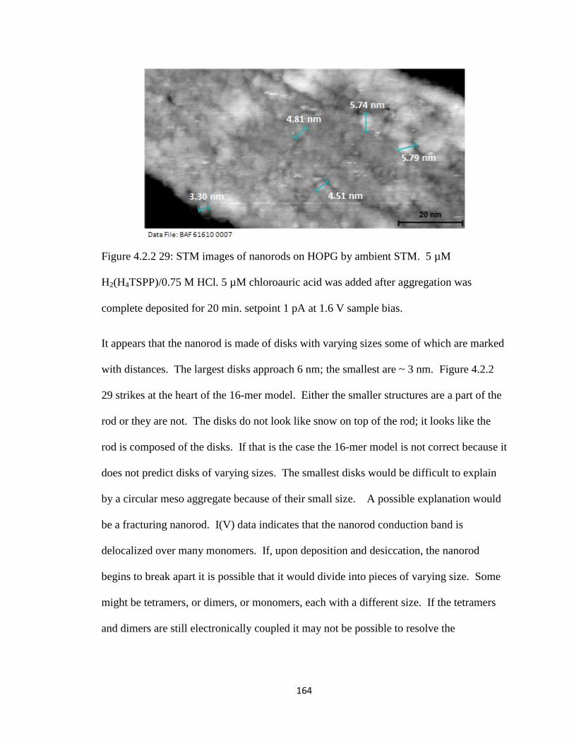
164
Figure 4.2.2 29: STM images of nanorods on HOPG by ambient STM. 5 µM
H2(H4TSPP)/0.75 M HCl. 5 µM chloroauric acid was added after aggregation was
complete deposited for 20 min. setpoint 1 pA at 1.6 V sample bias.
It appears that the nanorod is made of disks with varying sizes some of which are marked
with distances. The largest disks approach 6 nm; the smallest are ~ 3 nm. Figure 4.2.2
29 strikes at the heart of the 16-mer model. Either the smaller structures are a part of the
rod or they are not. The disks do not look like snow on top of the rod; it looks like the
rod is composed of the disks. If that is the case the 16-mer model is not correct because it
does not predict disks of varying sizes. The smallest disks would be difficult to explain
by a circular meso aggregate because of their small size. A possible explanation would
be a fracturing nanorod. I(V) data indicates that the nanorod conduction band is
delocalized over many monomers. If, upon deposition and desiccation, the nanorod
begins to break apart it is possible that it would divide into pieces of varying size. Some
might be tetramers, or dimers, or monomers, each with a different size. If the tetramers
and dimers are still electronically coupled it may not be possible to resolve the
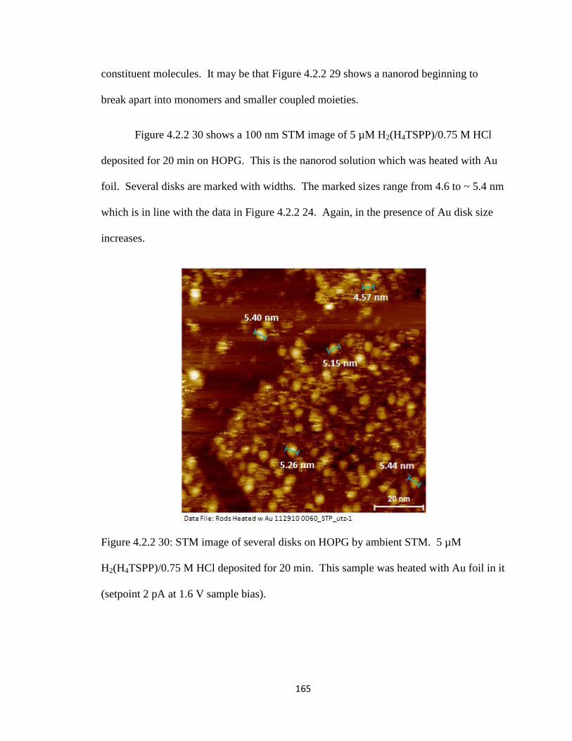
165
constituent molecules. It may be that Figure 4.2.2 29 shows a nanorod beginning to
break apart into monomers and smaller coupled moieties.
Figure 4.2.2 30 shows a 100 nm STM image of 5 µM H2(H4TSPP)/0.75 M HCl
deposited for 20 min on HOPG. This is the nanorod solution which was heated with Au
foil. Several disks are marked with widths. The marked sizes range from 4.6 to ~ 5.4 nm
which is in line with the data in Figure 4.2.2 24. Again, in the presence of Au disk size
increases.
Figure 4.2.2 30: STM image of several disks on HOPG by ambient STM. 5 µM
H2(H4TSPP)/0.75 M HCl deposited for 20 min. This sample was heated with Au foil in it
(setpoint 2 pA at 1.6 V sample bias).
166
It is important to emphasize that, at this point, we do not know what the disks are.
We also have not confirmed that they are all the same species. We have learned that
chloroauric acid and heating the nanorod solution with Au foil in it have similar effects
on disk size, namely increasing it. Figure 4.2.2 29 is the closest we have come to
reproducing the disk structure seen on Au(111). That sample was 5 µM in chloroauric
acid.
In order to address the possibilty that the disks are a product of a ripening process
on the HOPG surface 5 µM H2(H4TSPP)/0.75 M HCl was deposited on HOPG for 20, 30,
and 60 min. No gold was present in this system. The samples were scanned in air and a
histogram of the disk sizes was prepared. The data is presented in Figure 4.2.2 31. The
data in the three samples is grouped around ~4 nm, only a very few data points can be
seen around 6 nm. This data does not show a clear increase in the size of disks with
deposition time in the absence of Au.
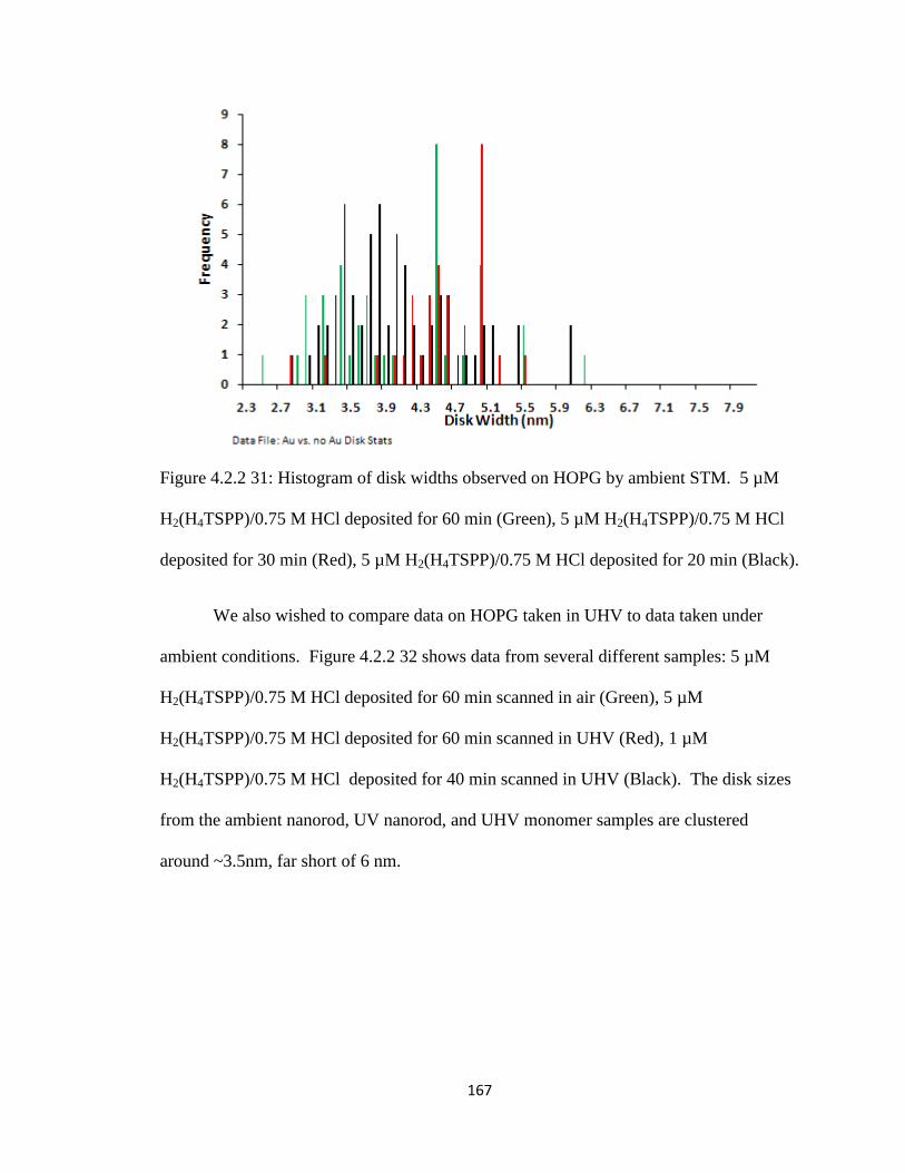
167
Figure 4.2.2 31: Histogram of disk widths observed on HOPG by ambient STM. 5 µM
H2(H4TSPP)/0.75 M HCl deposited for 60 min (Green), 5 µM H2(H4TSPP)/0.75 M HCl
deposited for 30 min (Red), 5 µM H2(H4TSPP)/0.75 M HCl deposited for 20 min (Black).
We also wished to compare data on HOPG taken in UHV to data taken under
ambient conditions. Figure 4.2.2 32 shows data from several different samples: 5 µM
H2(H4TSPP)/0.75 M HCl deposited for 60 min scanned in air (Green), 5 µM
H2(H4TSPP)/0.75 M HCl deposited for 60 min scanned in UHV (Red), 1 µM
H2(H4TSPP)/0.75 M HCl deposited for 40 min scanned in UHV (Black). The disk sizes
from the ambient nanorod, UV nanorod, and UHV monomer samples are clustered
around ~3.5nm, far short of 6 nm.
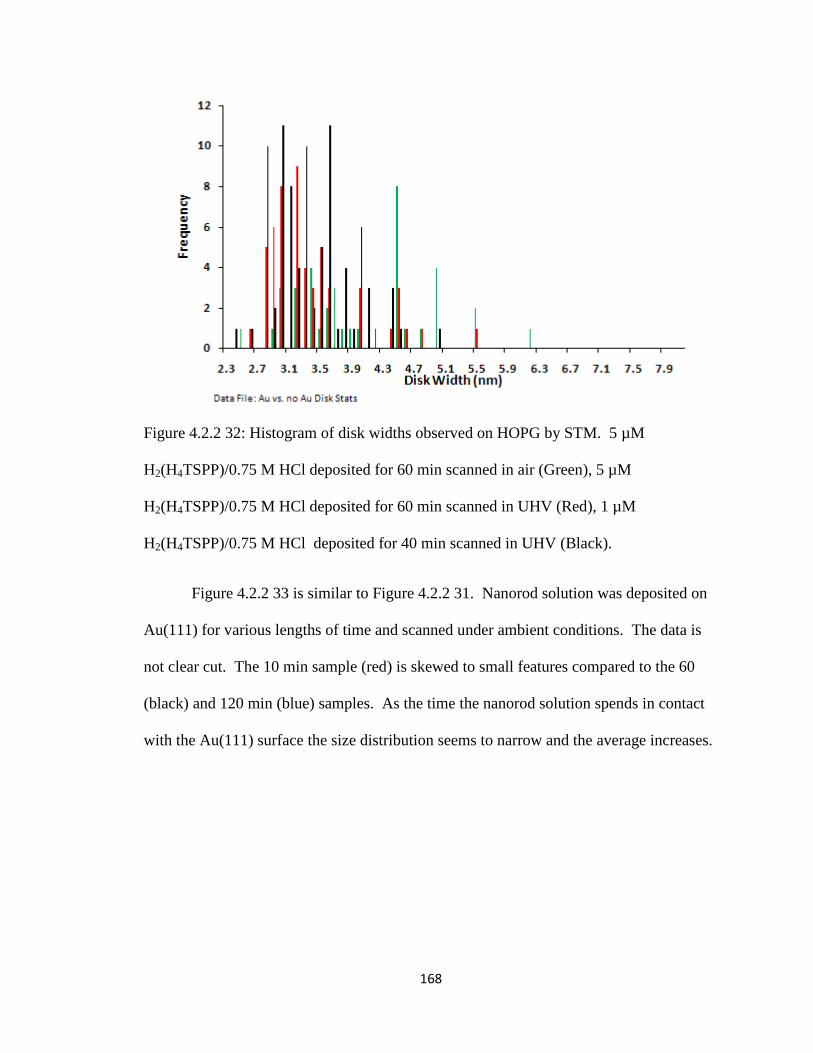
168
Figure 4.2.2 32: Histogram of disk widths observed on HOPG by STM. 5 µM
H2(H4TSPP)/0.75 M HCl deposited for 60 min scanned in air (Green), 5 µM
H2(H4TSPP)/0.75 M HCl deposited for 60 min scanned in UHV (Red), 1 µM
H2(H4TSPP)/0.75 M HCl deposited for 40 min scanned in UHV (Black).
Figure 4.2.2 33 is similar to Figure 4.2.2 31. Nanorod solution was deposited on
Au(111) for various lengths of time and scanned under ambient conditions. The data is
not clear cut. The 10 min sample (red) is skewed to small features compared to the 60
(black) and 120 min (blue) samples. As the time the nanorod solution spends in contact
with the Au(111) surface the size distribution seems to narrow and the average increases.
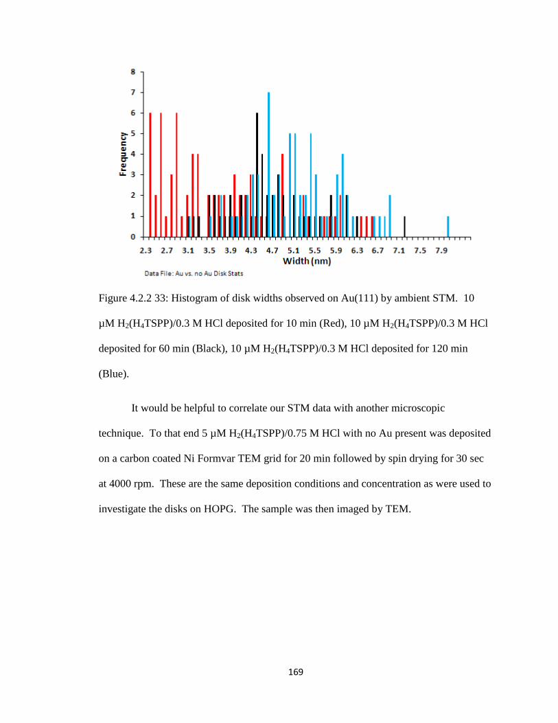
169
Figure 4.2.2 33: Histogram of disk widths observed on Au(111) by ambient STM. 10
µM H2(H4TSPP)/0.3 M HCl deposited for 10 min (Red), 10 µM H2(H4TSPP)/0.3 M HCl
deposited for 60 min (Black), 10 µM H2(H4TSPP)/0.3 M HCl deposited for 120 min
(Blue).
It would be helpful to correlate our STM data with another microscopic
technique. To that end 5 µM H2(H4TSPP)/0.75 M HCl with no Au present was deposited
on a carbon coated Ni Formvar TEM grid for 20 min followed by spin drying for 30 sec
at 4000 rpm. These are the same deposition conditions and concentration as were used to
investigate the disks on HOPG. The sample was then imaged by TEM.
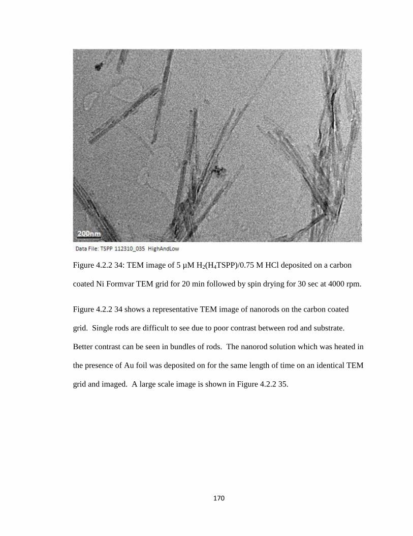
170
Figure 4.2.2 34: TEM image of 5 µM H2(H4TSPP)/0.75 M HCl deposited on a carbon
coated Ni Formvar TEM grid for 20 min followed by spin drying for 30 sec at 4000 rpm.
Figure 4.2.2 34 shows a representative TEM image of nanorods on the carbon coated
grid. Single rods are difficult to see due to poor contrast between rod and substrate.
Better contrast can be seen in bundles of rods. The nanorod solution which was heated in
the presence of Au foil was deposited on for the same length of time on an identical TEM
grid and imaged. A large scale image is shown in Figure 4.2.2 35.
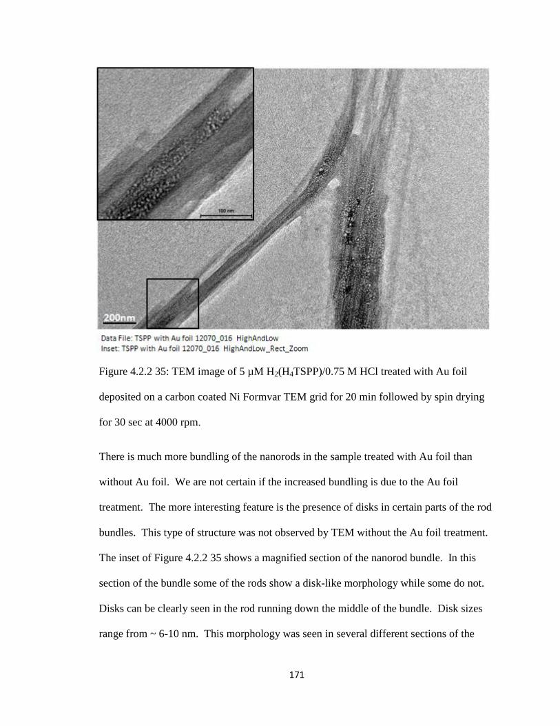
171
Figure 4.2.2 35: TEM image of 5 µM H2(H4TSPP)/0.75 M HCl treated with Au foil
deposited on a carbon coated Ni Formvar TEM grid for 20 min followed by spin drying
for 30 sec at 4000 rpm.
There is much more bundling of the nanorods in the sample treated with Au foil than
without Au foil. We are not certain if the increased bundling is due to the Au foil
treatment. The more interesting feature is the presence of disks in certain parts of the rod
bundles. This type of structure was not observed by TEM without the Au foil treatment.
The inset of Figure 4.2.2 35 shows a magnified section of the nanorod bundle. In this
section of the bundle some of the rods show a disk-like morphology while some do not.
Disks can be clearly seen in the rod running down the middle of the bundle. Disk sizes
range from ~ 6-10 nm. This morphology was seen in several different sections of the

172
TEM grid and on different samples. Figure 4.2.2 36 shows a smaller image of the
intersection of the two rod bundles. The same type of morphology can be seen in Figure
4.2.2 36; some of the rods have disks and some do not.
Figure 4.2.2 36: TEM image of 5 µM H2(H4TSPP)/0.75 M HCl treated with Au foil
deposited on a carbon coated Ni Formvar TEM grid for 20 min followed by spin drying
for 30 sec at 4000 rpm.
Figure 4.2.2 37 is the highest magnification TEM image of a nanorod bundle we have
taken. In this image the “disks” look more like rectangles than true disks. The diameter
of the structures ranges ~ 5-10 nm, about twice as big as the disks seen in STM. The
TEM images of H2(H4TSPP) with and without exposure to Au foil do not lend support to
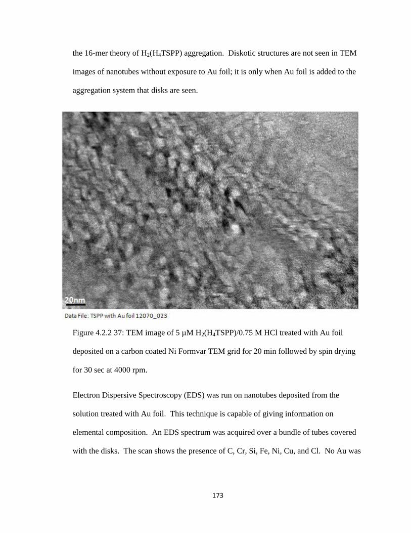
173
the 16-mer theory of H2(H4TSPP) aggregation. Diskotic structures are not seen in TEM
images of nanotubes without exposure to Au foil; it is only when Au foil is added to the
aggregation system that disks are seen.
Figure 4.2.2 37: TEM image of 5 µM H2(H4TSPP)/0.75 M HCl treated with Au foil
deposited on a carbon coated Ni Formvar TEM grid for 20 min followed by spin drying
for 30 sec at 4000 rpm.
Electron Dispersive Spectroscopy (EDS) was run on nanotubes deposited from the
solution treated with Au foil. This technique is capable of giving information on
elemental composition. An EDS spectrum was acquired over a bundle of tubes covered
with the disks. The scan shows the presence of C, Cr, Si, Fe, Ni, Cu, and Cl. No Au was
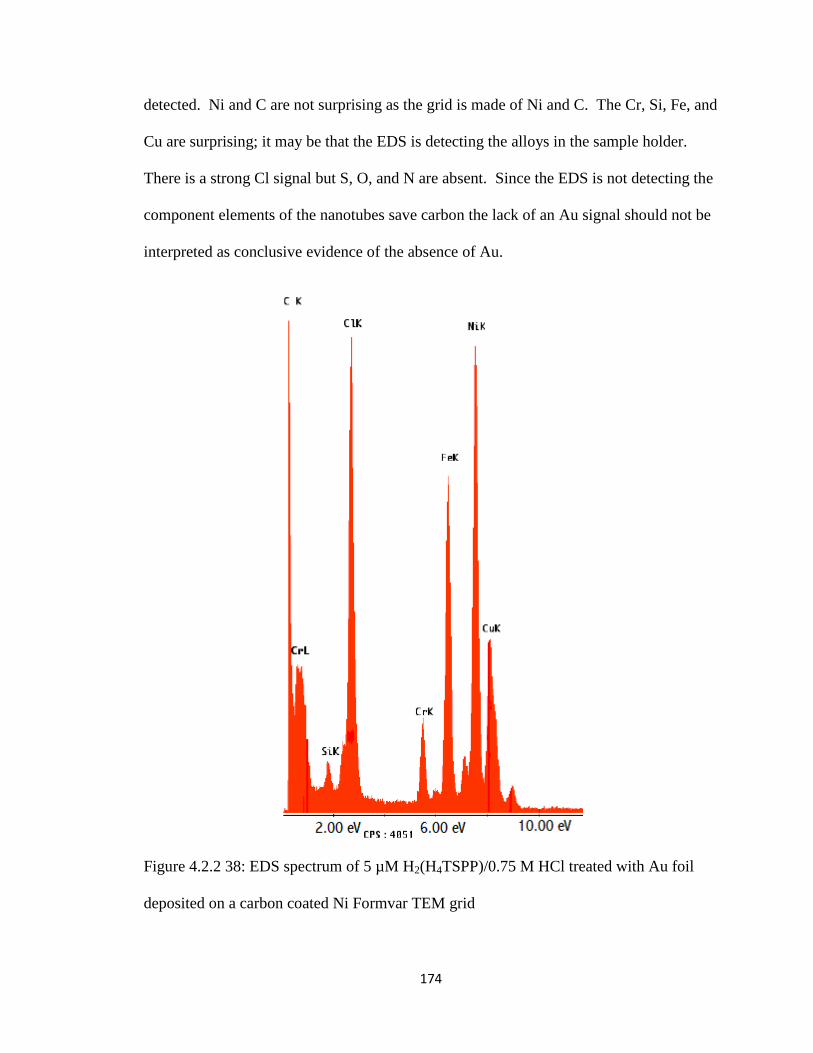
174
detected. Ni and C are not surprising as the grid is made of Ni and C. The Cr, Si, Fe, and
Cu are surprising; it may be that the EDS is detecting the alloys in the sample holder.
There is a strong Cl signal but S, O, and N are absent. Since the EDS is not detecting the
component elements of the nanotubes save carbon the lack of an Au signal should not be
interpreted as conclusive evidence of the absence of Au.
Figure 4.2.2 38: EDS spectrum of 5 µM H2(H4TSPP)/0.75 M HCl treated with Au foil
deposited on a carbon coated Ni Formvar TEM grid
175
We have reported on a number of experiments on the relationship between the
disks observed in STM images of the H2(H4TSPP) aggregate system. In the presence of
either metallic Au or chloroauric acid the size of the disks increases. TEM images show
that disks are present only when the aggregate solution was exposed to Au foil. We have
not been able to identify the structure of the disks, but the data presented in this section
indicates that the presence of Au is intimately correlated with their size; with increasing
gold exposure leading to larger disks. After analysis of the data it is likely that the disk
model of H2(H4TSPP) aggregation is not correct and the disks are a result of a side
reaction with Au.
4.3 Characterization of Tetrasulfonatophenyl Porphyrin and its Aggregate by
Raman and Resonance Raman Spectroscopy
Before presenting Raman data on TSPP and its aggregate it is worthwhile to cover
the naming convention which will be used to identify normal modes. Figure 4.3 1 shows
the system which will be used to keep track of vibrational modes.
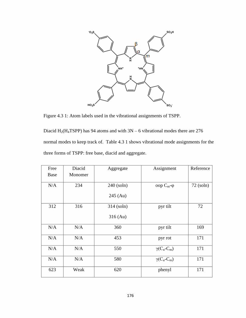
176
Figure 4.3 1: Atom labels used in the vibrational assignments of TSPP.
Diacid H2(H4TSPP) has 94 atoms and with 3N – 6 vibrational modes there are 276
normal modes to keep track of. Table 4.3 1 shows vibrational mode assignments for the
three forms of TSPP: free base, diacid and aggregate.
Free
Base
Diacid
Monomer
Aggregate Assignment Reference
N/A 234 240 (soln)
245 (Au)
oop Cm-φ 72 (soln)
312 316 314 (soln)
316 (Au)
pyr tilt 72
N/A N/A 360 pyr tilt 169
N/A N/A 453 pyr rot 171
N/A N/A 550 γ(Cα-Cm) 171
N/A N/A 580 γ(Cα-Cm) 171
623 Weak 620 phenyl 171
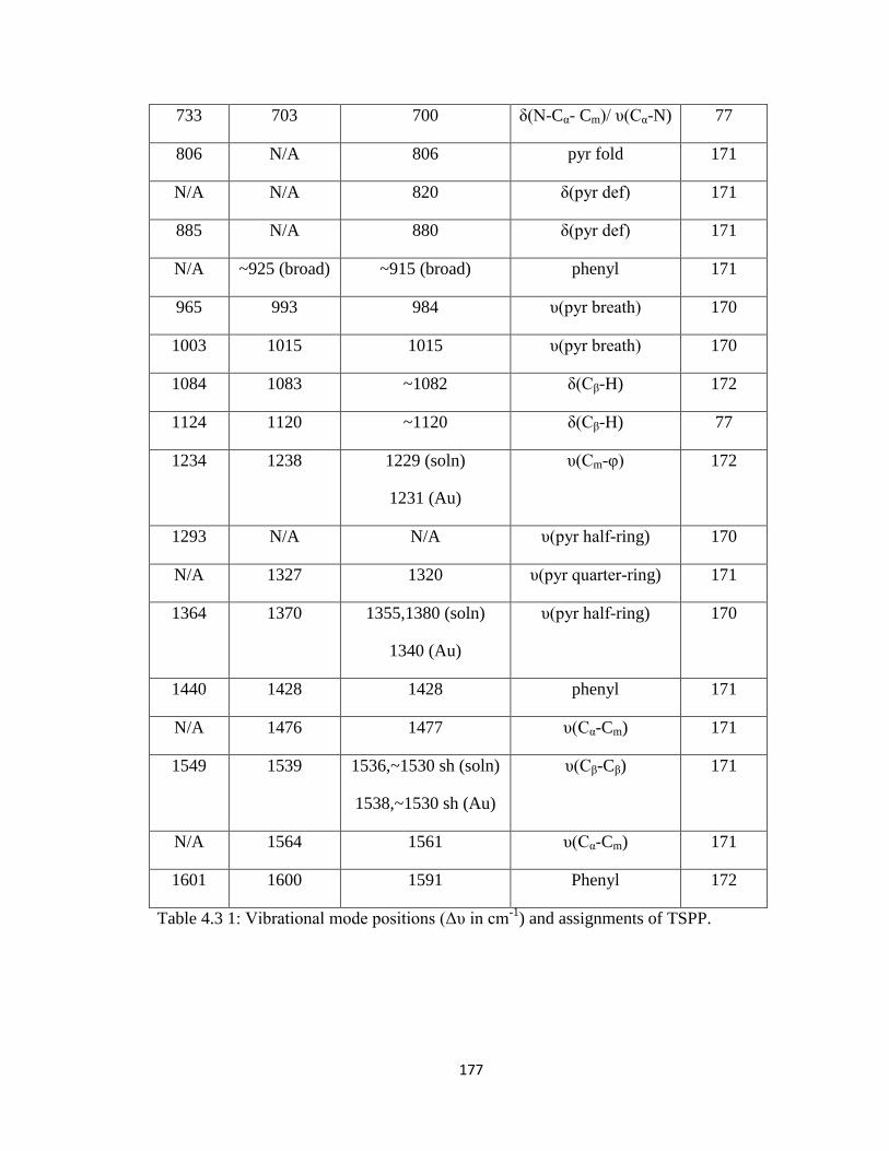
177
733 703 700 δ(N-Cα- Cm)/ υ(Cα-N) 77
806 N/A 806 pyr fold 171
N/A N/A 820 δ(pyr def) 171
885 N/A 880 δ(pyr def) 171
N/A ~925 (broad) ~915 (broad) phenyl 171
965 993 984 υ(pyr breath) 170
1003 1015 1015 υ(pyr breath) 170
1084 1083 ~1082 δ(Cβ-H) 172
1124 1120 ~1120 δ(Cβ-H) 77
1234 1238 1229 (soln)
1231 (Au)
υ(Cm-φ) 172
1293 N/A N/A υ(pyr half-ring) 170
N/A 1327 1320 υ(pyr quarter-ring) 171
1364 1370 1355,1380 (soln)
1340 (Au)
υ(pyr half-ring) 170
1440 1428 1428 phenyl 171
N/A 1476 1477 υ(Cα-Cm) 171
1549 1539 1536,~1530 sh (soln)
1538,~1530 sh (Au)
υ(Cβ-Cβ) 171
N/A 1564 1561 υ(Cα-Cm) 171
1601 1600 1591 Phenyl 172
Table 4.3 1: Vibrational mode positions (Δυ in cm-1
) and assignments of TSPP.
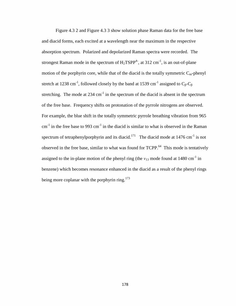
178
Figure 4.3 2 and Figure 4.3 3 show solution phase Raman data for the free base
and diacid forms, each excited at a wavelength near the maximum in the respective
absorption spectrum. Polarized and depolarized Raman spectra were recorded. The
strongest Raman mode in the spectrum of H2TSPP4-
, at 312 cm-1
, is an out-of-plane
motion of the porphyrin core, while that of the diacid is the totally symmetric Cm-phenyl
stretch at 1238 cm-1
, followed closely by the band at 1539 cm-1
assigned to Cβ-Cβ
stretching. The mode at 234 cm-1
in the spectrum of the diacid is absent in the spectrum
of the free base. Frequency shifts on protonation of the pyrrole nitrogens are observed.
For example, the blue shift in the totally symmetric pyrrole breathing vibration from 965
cm-1
in the free base to 993 cm-1
in the diacid is similar to what is observed in the Raman
spectrum of tetraphenylporphyrin and its diacid.171
The diacid mode at 1476 cm-1
is not
observed in the free base, similar to what was found for TCPP.64
This mode is tentatively
assigned to the in-plane motion of the phenyl ring (the ν13 mode found at 1480 cm-1
in
benzene) which becomes resonance enhanced in the diacid as a result of the phenyl rings
being more coplanar with the porphyrin ring.173
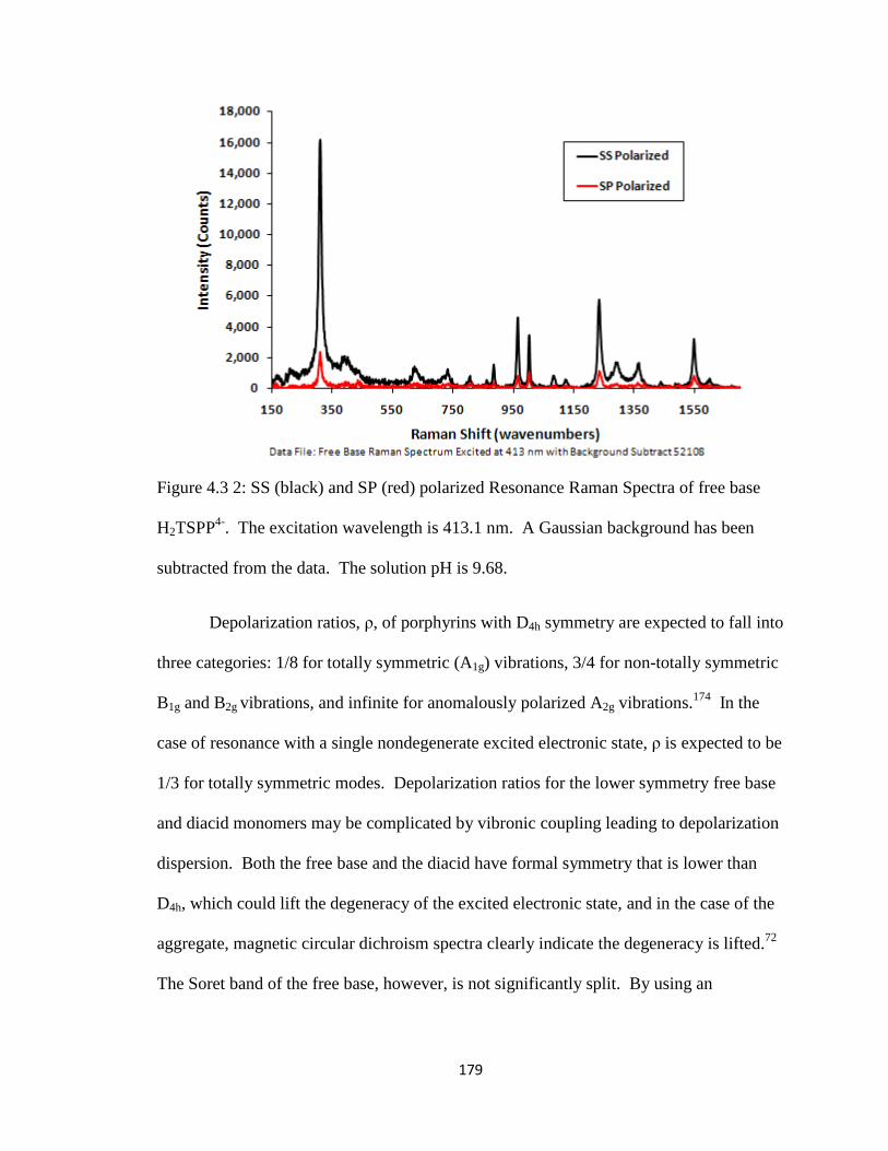
179
Figure 4.3 2: SS (black) and SP (red) polarized Resonance Raman Spectra of free base
H2TSPP4-
. The excitation wavelength is 413.1 nm. A Gaussian background has been
subtracted from the data. The solution pH is 9.68.
Depolarization ratios, ρ, of porphyrins with D4h symmetry are expected to fall into
three categories: 1/8 for totally symmetric (A1g) vibrations, 3/4 for non-totally symmetric
B1g and B2g vibrations, and infinite for anomalously polarized A2g vibrations.174
In the
case of resonance with a single nondegenerate excited electronic state, ρ is expected to be
1/3 for totally symmetric modes. Depolarization ratios for the lower symmetry free base
and diacid monomers may be complicated by vibronic coupling leading to depolarization
dispersion. Both the free base and the diacid have formal symmetry that is lower than
D4h, which could lift the degeneracy of the excited electronic state, and in the case of the
aggregate, magnetic circular dichroism spectra clearly indicate the degeneracy is lifted.72
The Soret band of the free base, however, is not significantly split. By using an
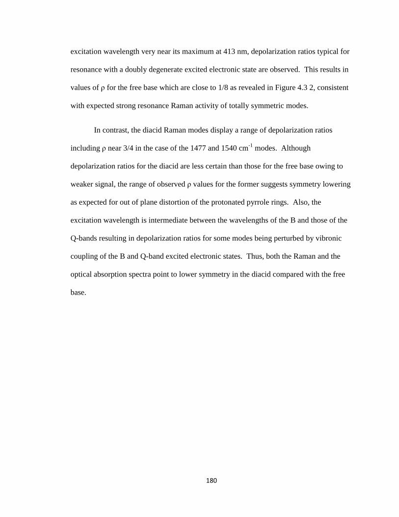
180
excitation wavelength very near its maximum at 413 nm, depolarization ratios typical for
resonance with a doubly degenerate excited electronic state are observed. This results in
values of ρ for the free base which are close to 1/8 as revealed in Figure 4.3 2, consistent
with expected strong resonance Raman activity of totally symmetric modes.
In contrast, the diacid Raman modes display a range of depolarization ratios
including ρ near 3/4 in the case of the 1477 and 1540 cm-1
modes. Although
depolarization ratios for the diacid are less certain than those for the free base owing to
weaker signal, the range of observed ρ values for the former suggests symmetry lowering
as expected for out of plane distortion of the protonated pyrrole rings. Also, the
excitation wavelength is intermediate between the wavelengths of the B and those of the
Q-bands resulting in depolarization ratios for some modes being perturbed by vibronic
coupling of the B and Q-band excited electronic states. Thus, both the Raman and the
optical absorption spectra point to lower symmetry in the diacid compared with the free
base.
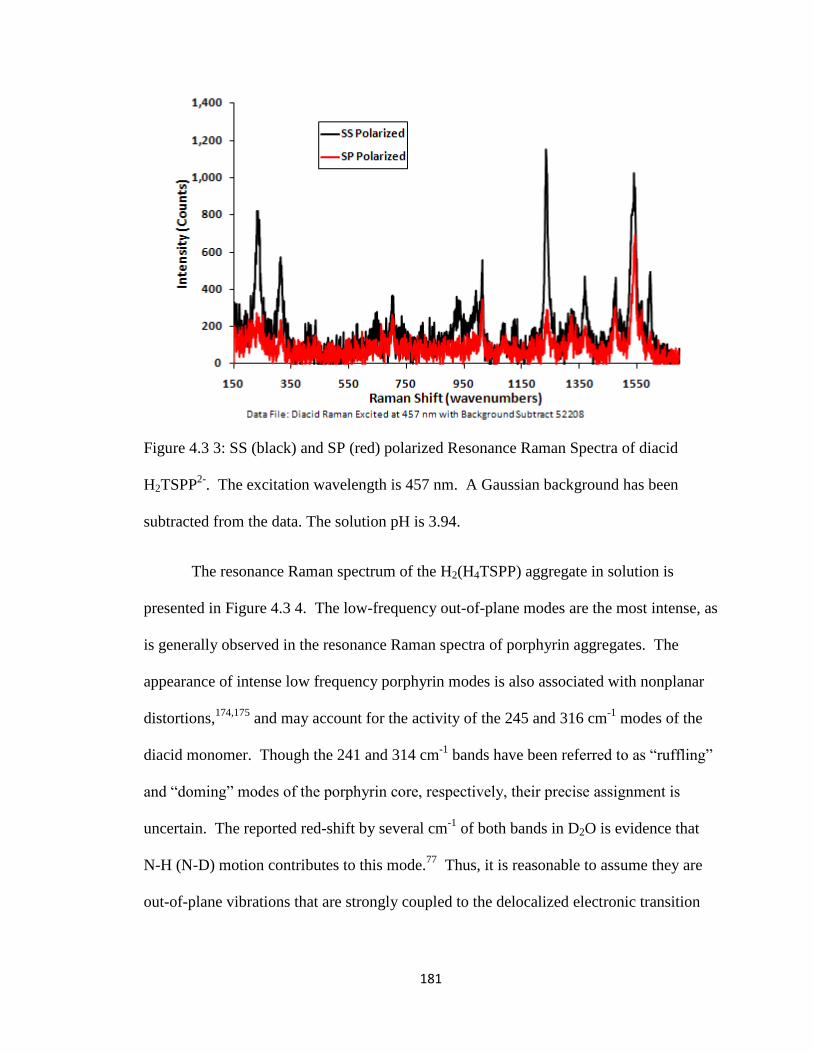
181
Figure 4.3 3: SS (black) and SP (red) polarized Resonance Raman Spectra of diacid
H2TSPP2-
. The excitation wavelength is 457 nm. A Gaussian background has been
subtracted from the data. The solution pH is 3.94.
The resonance Raman spectrum of the H2(H4TSPP) aggregate in solution is
presented in Figure 4.3 4. The low-frequency out-of-plane modes are the most intense, as
is generally observed in the resonance Raman spectra of porphyrin aggregates. The
appearance of intense low frequency porphyrin modes is also associated with nonplanar
distortions,174,175
and may account for the activity of the 245 and 316 cm-1
modes of the
diacid monomer. Though the 241 and 314 cm-1
bands have been referred to as “ruffling”
and “doming” modes of the porphyrin core, respectively, their precise assignment is
uncertain. The reported red-shift by several cm-1
of both bands in D2O is evidence that
N-H (N-D) motion contributes to this mode.77
Thus, it is reasonable to assume they are
out-of-plane vibrations that are strongly coupled to the delocalized electronic transition
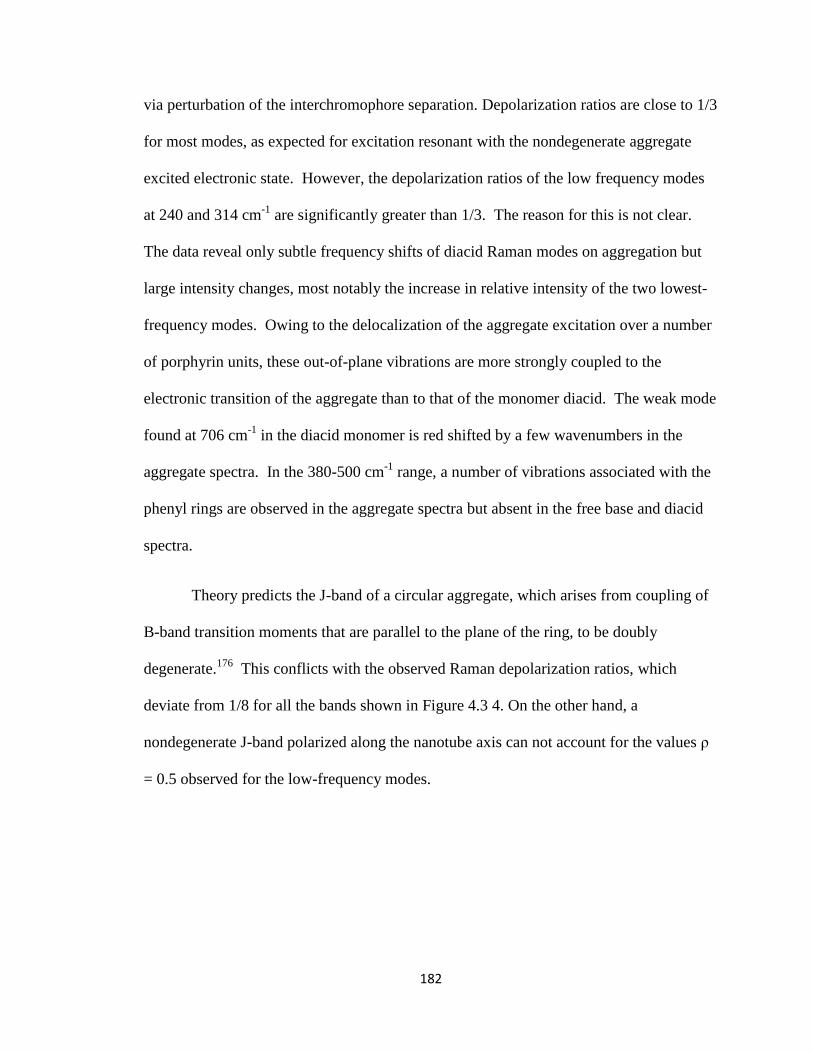
182
via perturbation of the interchromophore separation. Depolarization ratios are close to 1/3
for most modes, as expected for excitation resonant with the nondegenerate aggregate
excited electronic state. However, the depolarization ratios of the low frequency modes
at 240 and 314 cm-1
are significantly greater than 1/3. The reason for this is not clear.
The data reveal only subtle frequency shifts of diacid Raman modes on aggregation but
large intensity changes, most notably the increase in relative intensity of the two lowest-
frequency modes. Owing to the delocalization of the aggregate excitation over a number
of porphyrin units, these out-of-plane vibrations are more strongly coupled to the
electronic transition of the aggregate than to that of the monomer diacid. The weak mode
found at 706 cm-1
in the diacid monomer is red shifted by a few wavenumbers in the
aggregate spectra. In the 380-500 cm-1
range, a number of vibrations associated with the
phenyl rings are observed in the aggregate spectra but absent in the free base and diacid
spectra.
Theory predicts the J-band of a circular aggregate, which arises from coupling of
B-band transition moments that are parallel to the plane of the ring, to be doubly
degenerate.176
This conflicts with the observed Raman depolarization ratios, which
deviate from 1/8 for all the bands shown in Figure 4.3 4. On the other hand, a
nondegenerate J-band polarized along the nanotube axis can not account for the values ρ
= 0.5 observed for the low-frequency modes.
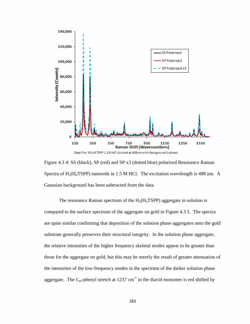
183
Figure 4.3 4: SS (black), SP (red) and SP x3 (dotted blue) polarized Resonance Raman
Spectra of H2(H4TSPP) nanorods in 1.5 M HCl. The excitation wavelength is 488 nm. A
Gaussian background has been subtracted from the data.
The resonance Raman spectrum of the H2(H4TSPP) aggregate in solution is
compared to the surface spectrum of the aggregate on gold in Figure 4.3 5. The spectra
are quite similar confirming that deposition of the solution phase aggregates onto the gold
substrate generally preserves their structural integrity. In the solution phase aggregate,
the relative intensities of the higher frequency skeletal modes appear to be greater than
those for the aggregate on gold, but this may be merely the result of greater attenuation of
the intensities of the low-frequency modes in the spectrum of the darker solution phase
aggregate. The Cm-phenyl stretch at 1237 cm-1
in the diacid monomer is red shifted by
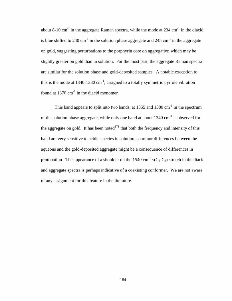
184
about 8-10 cm-1
in the aggregate Raman spectra, while the mode at 234 cm-1
in the diacid
is blue shifted to 240 cm-1
in the solution phase aggregate and 245 cm-1
in the aggregate
on gold, suggesting perturbations to the porphyrin core on aggregation which may be
slightly greater on gold than in solution. For the most part, the aggregate Raman spectra
are similar for the solution phase and gold-deposited samples. A notable exception to
this is the mode at 1340-1380 cm-1
, assigned to a totally symmetric pyrrole vibration
found at 1370 cm-1
in the diacid monomer.
This band appears to split into two bands, at 1355 and 1380 cm-1
in the spectrum
of the solution phase aggregate, while only one band at about 1340 cm-1
is observed for
the aggregate on gold. It has been noted171
that both the frequency and intensity of this
band are very sensitive to acidic species in solution, so minor differences between the
aqueous and the gold-deposited aggregate might be a consequence of differences in
protonation. The appearance of a shoulder on the 1540 cm-1
ν(Cβ-Cβ) stretch in the diacid
and aggregate spectra is perhaps indicative of a coexisting conformer. We are not aware
of any assignment for this feature in the literature.
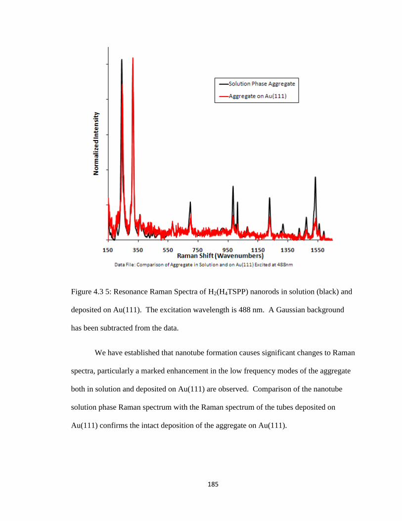
185
Figure 4.3 5: Resonance Raman Spectra of H2(H4TSPP) nanorods in solution (black) and
deposited on Au(111). The excitation wavelength is 488 nm. A Gaussian background
has been subtracted from the data.
We have established that nanotube formation causes significant changes to Raman
spectra, particularly a marked enhancement in the low frequency modes of the aggregate
both in solution and deposited on Au(111) are observed. Comparison of the nanotube
solution phase Raman spectrum with the Raman spectrum of the tubes deposited on
Au(111) confirms the intact deposition of the aggregate on Au(111).
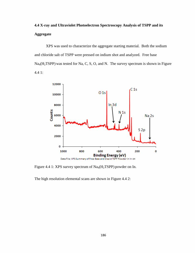
186
4.4 X-ray and Ultraviolet Photoelectron Spectroscopy Analysis of TSPP and its
Aggregate
XPS was used to characterize the aggregate starting material. Both the sodium
and chloride salt of TSPP were pressed on indium shot and analyzed. Free base
Na4(H2TSPP) was tested for Na, C, S, O, and N. The survey spectrum is shown in Figure
4.4 1:
Figure 4.4 1: XPS survey spectrum of Na4(H2TSPP) powder on In.
The high resolution elemental scans are shown in Figure 4.4 2:
on
187
Figure 4.4 2: XPS sulfur, carbon, oxygen, and sodium spectra of Na4(H2TSPP) powder on
In.
The scans have good signal to noise, and the 2p1/2/2p3/2 spin orbit splitting can be seen in
the sulfur 2p scan. The sulfur peak is located at 167 eV which is the expected position
for a sulfonic acid group177
. The small broad peak at ~ 162 eV is worth noting, the 162
eV peak may be a result of contaminants in the powder as this is the region where sulfide
is found.178
The diacid H4(H4TSPP)Cl2 powder was also analyzed, the survey is shown in
Figure 4.4 3:
on
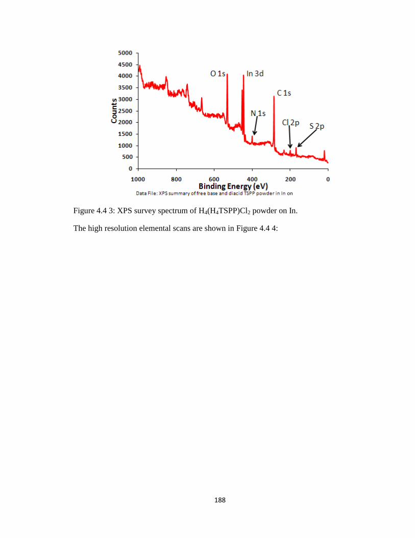
188
Figure 4.4 3: XPS survey spectrum of H4(H4TSPP)Cl2 powder on In.
The high resolution elemental scans are shown in Figure 4.4 4:
on
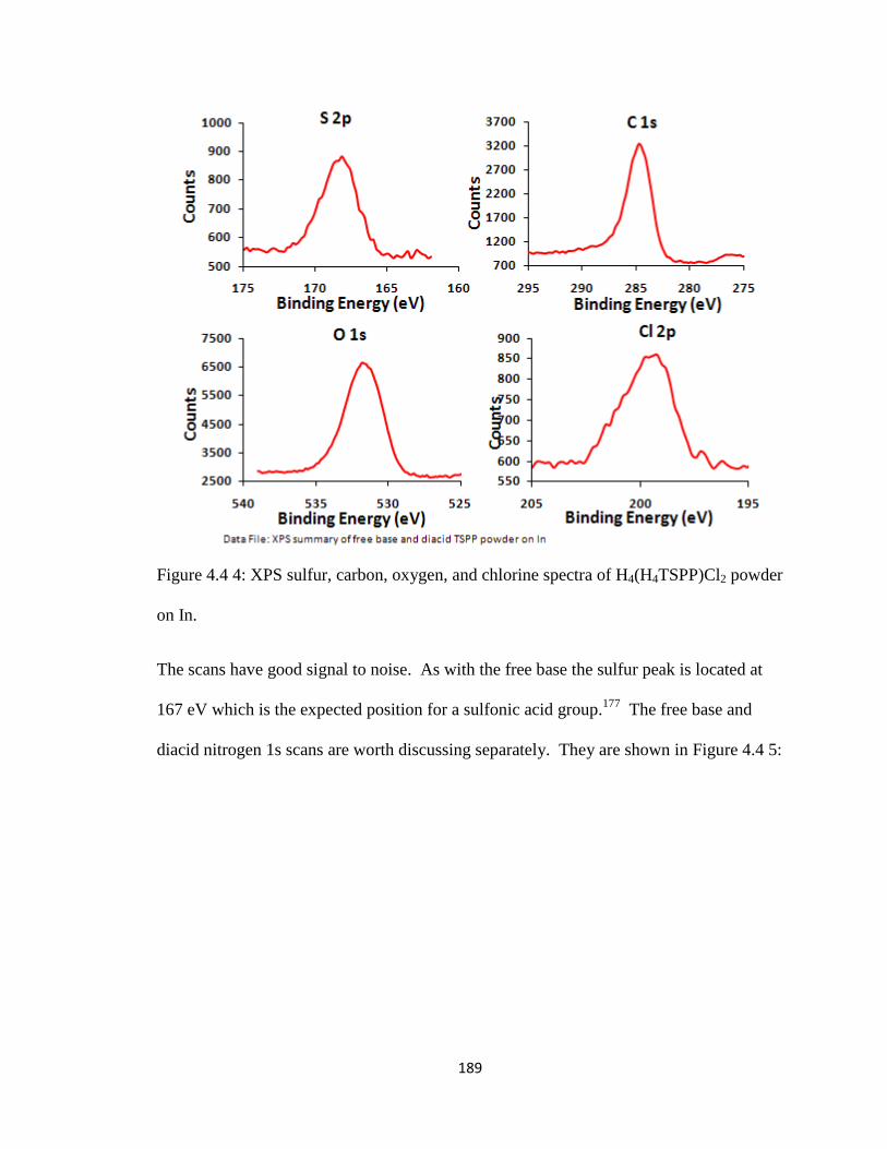
189
Figure 4.4 4: XPS sulfur, carbon, oxygen, and chlorine spectra of H4(H4TSPP)Cl2 powder
on In.
The scans have good signal to noise. As with the free base the sulfur peak is located at
167 eV which is the expected position for a sulfonic acid group.177
The free base and
diacid nitrogen 1s scans are worth discussing separately. They are shown in Figure 4.4 5:
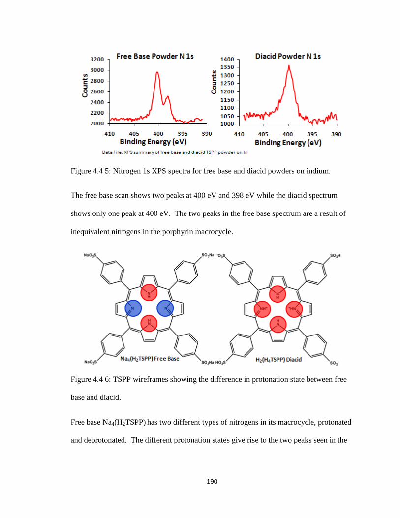
190
Figure 4.4 5: Nitrogen 1s XPS spectra for free base and diacid powders on indium.
The free base scan shows two peaks at 400 eV and 398 eV while the diacid spectrum
shows only one peak at 400 eV. The two peaks in the free base spectrum are a result of
inequivalent nitrogens in the porphyrin macrocycle.
Figure 4.4 6: TSPP wireframes showing the difference in protonation state between free
base and diacid.
Free base Na4(H2TSPP) has two different types of nitrogens in its macrocycle, protonated
and deprotonated. The different protonation states give rise to the two peaks seen in the
191
free base scan. The peak at 400 eV is associated with protonated nitrogen, the peak at
398 eV arises from deprotonated nitrogen.179
The disparity in peak size is due to the
relative amounts of protonated and unprotonated nitrogen. The free base N 1s spectrum
is the sum of two spectra, the free base and “contamination” by diacid. If the diacid form
is present in the free base powder the 400 eV peak will increase in intensity compared to
the 398 eV peak; which is exactly what we see in the free base scan. This mix of two
spectra has been previously reported in tetrakis(p-carboxyphenyl)porphyrin.179
The elemental ratios of the free base and diacid were calculated from their
respective spectra and the theoretical atomic ratios are presented in the Table 4.4 1:
Element
Experimental
Free Base Ratios
Experimental
Diacid Ratios
Theoretical Free
Base Ratios
Theoretical
Diacid Ratios
O 3.4 3.8 3.0 3.0
N 1.0 1.0 1.0 1.0
C 8.8 11.0 11.0 11.0
S 1.0 1.0 1.0 1.0
Na 0.93 N/A 1.0 N/A
Cl N/A 0.18 N/A 0.50
Table 4.4 1: Theoretical and experimental elemental ratios in TSPP free base and diacid
powders.
For clarity the ratios have been normalized to sulfur. Carbon aside, the elemental ratios
in the free base work out as expected. Oxygen is higher than expected, but this can be
attributed to waters of hydration. The free base powder is a dodecahydrate; the extra
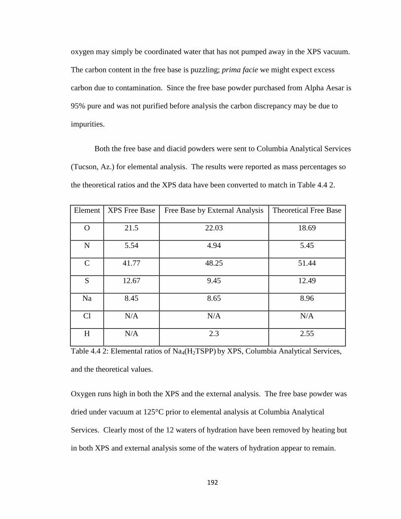
192
oxygen may simply be coordinated water that has not pumped away in the XPS vacuum.
The carbon content in the free base is puzzling; prima facie we might expect excess
carbon due to contamination. Since the free base powder purchased from Alpha Aesar is
95% pure and was not purified before analysis the carbon discrepancy may be due to
impurities.
Both the free base and diacid powders were sent to Columbia Analytical Services
(Tucson, Az.) for elemental analysis. The results were reported as mass percentages so
the theoretical ratios and the XPS data have been converted to match in Table 4.4 2.
Element XPS Free Base Free Base by External Analysis Theoretical Free Base
O 21.5 22.03 18.69
N 5.54 4.94 5.45
C 41.77 48.25 51.44
S 12.67 9.45 12.49
Na 8.45 8.65 8.96
Cl N/A N/A N/A
H N/A 2.3 2.55
Table 4.4 2: Elemental ratios of Na4(H2TSPP) by XPS, Columbia Analytical Services,
and the theoretical values.
Oxygen runs high in both the XPS and the external analysis. The free base powder was
dried under vacuum at 125°C prior to elemental analysis at Columbia Analytical
Services. Clearly most of the 12 waters of hydration have been removed by heating but
in both XPS and external analysis some of the waters of hydration appear to remain.
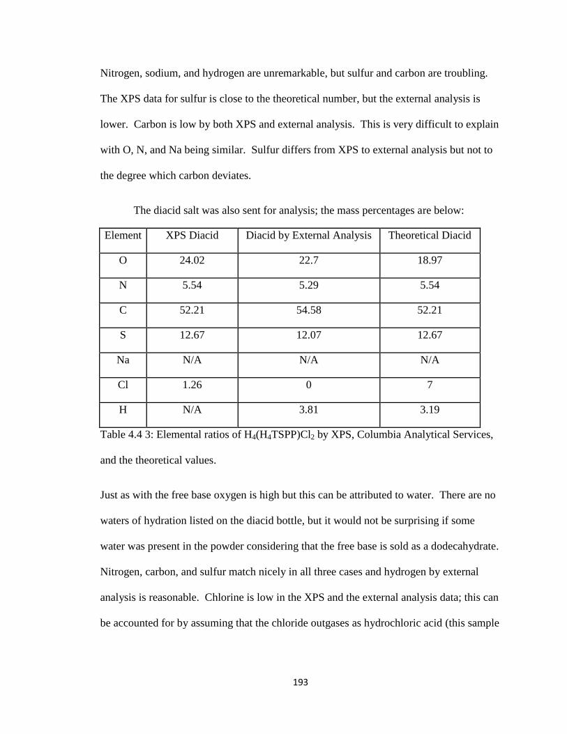
193
Nitrogen, sodium, and hydrogen are unremarkable, but sulfur and carbon are troubling.
The XPS data for sulfur is close to the theoretical number, but the external analysis is
lower. Carbon is low by both XPS and external analysis. This is very difficult to explain
with O, N, and Na being similar. Sulfur differs from XPS to external analysis but not to
the degree which carbon deviates.
The diacid salt was also sent for analysis; the mass percentages are below:
Element XPS Diacid Diacid by External Analysis Theoretical Diacid
O 24.02 22.7 18.97
N 5.54 5.29 5.54
C 52.21 54.58 52.21
S 12.67 12.07 12.67
Na N/A N/A N/A
Cl 1.26 0 7
H N/A 3.81 3.19
Table 4.4 3: Elemental ratios of H4(H4TSPP)Cl2 by XPS, Columbia Analytical Services,
and the theoretical values.
Just as with the free base oxygen is high but this can be attributed to water. There are no
waters of hydration listed on the diacid bottle, but it would not be surprising if some
water was present in the powder considering that the free base is sold as a dodecahydrate.
Nitrogen, carbon, and sulfur match nicely in all three cases and hydrogen by external
analysis is reasonable. Chlorine is low in the XPS and the external analysis data; this can
be accounted for by assuming that the chloride outgases as hydrochloric acid (this sample
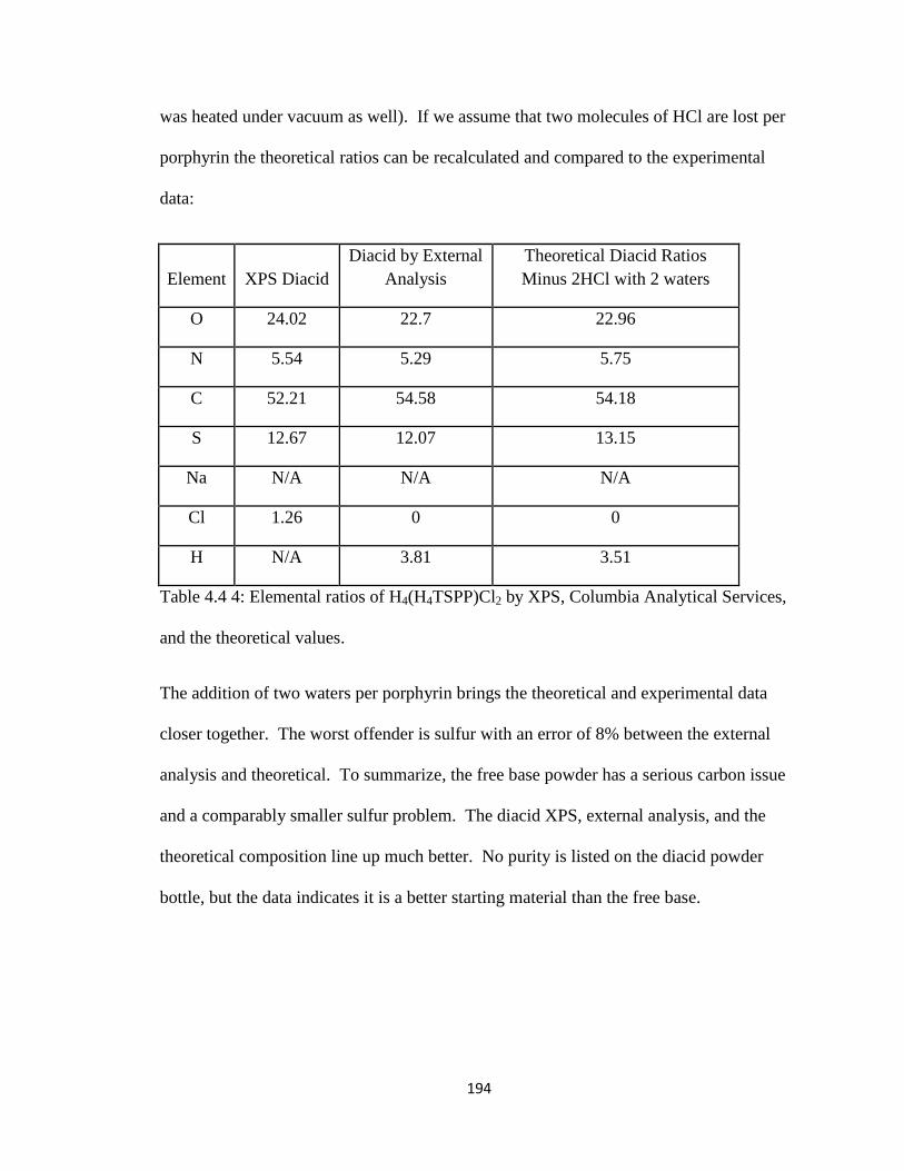
194
was heated under vacuum as well). If we assume that two molecules of HCl are lost per
porphyrin the theoretical ratios can be recalculated and compared to the experimental
data:
Element XPS Diacid
Diacid by External
Analysis
Theoretical Diacid Ratios
Minus 2HCl with 2 waters
O 24.02 22.7 22.96
N 5.54 5.29 5.75
C 52.21 54.58 54.18
S 12.67 12.07 13.15
Na N/A N/A N/A
Cl 1.26 0 0
H N/A 3.81 3.51
Table 4.4 4: Elemental ratios of H4(H4TSPP)Cl2 by XPS, Columbia Analytical Services,
and the theoretical values.
The addition of two waters per porphyrin brings the theoretical and experimental data
closer together. The worst offender is sulfur with an error of 8% between the external
analysis and theoretical. To summarize, the free base powder has a serious carbon issue
and a comparably smaller sulfur problem. The diacid XPS, external analysis, and the
theoretical composition line up much better. No purity is listed on the diacid powder
bottle, but the data indicates it is a better starting material than the free base.
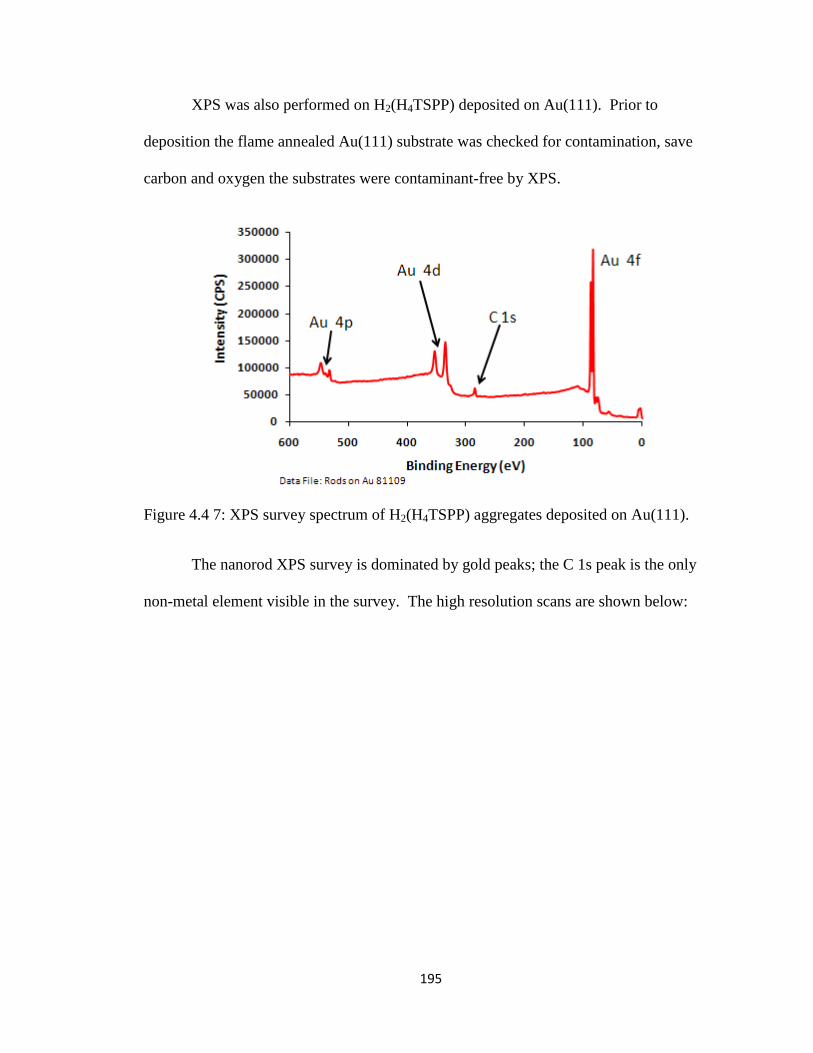
195
XPS was also performed on H2(H4TSPP) deposited on Au(111). Prior to
deposition the flame annealed Au(111) substrate was checked for contamination, save
carbon and oxygen the substrates were contaminant-free by XPS.
Figure 4.4 7: XPS survey spectrum of H2(H4TSPP) aggregates deposited on Au(111).
The nanorod XPS survey is dominated by gold peaks; the C 1s peak is the only
non-metal element visible in the survey. The high resolution scans are shown below:
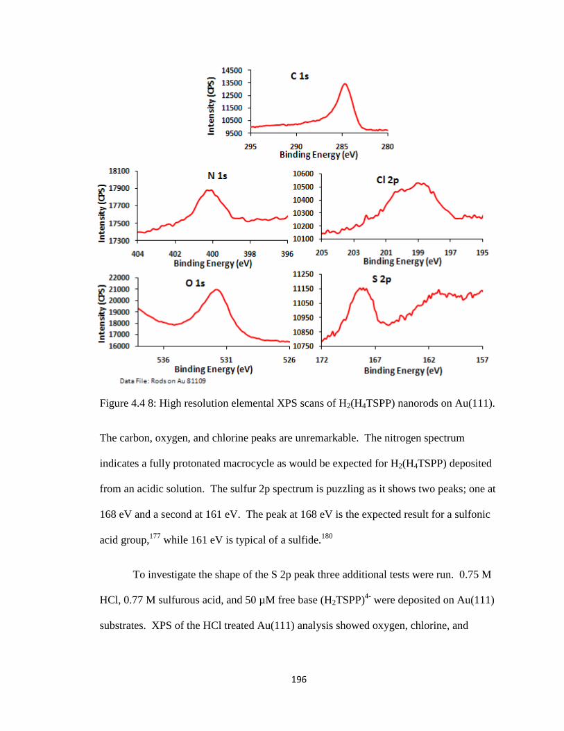
196
Figure 4.4 8: High resolution elemental XPS scans of H2(H4TSPP) nanorods on Au(111).
The carbon, oxygen, and chlorine peaks are unremarkable. The nitrogen spectrum
indicates a fully protonated macrocycle as would be expected for H2(H4TSPP) deposited
from an acidic solution. The sulfur 2p spectrum is puzzling as it shows two peaks; one at
168 eV and a second at 161 eV. The peak at 168 eV is the expected result for a sulfonic
acid group,177
while 161 eV is typical of a sulfide.180
To investigate the shape of the S 2p peak three additional tests were run. 0.75 M
HCl, 0.77 M sulfurous acid, and 50 µM free base (H2TSPP)4-
were deposited on Au(111)
substrates. XPS of the HCl treated Au(111) analysis showed oxygen, chlorine, and
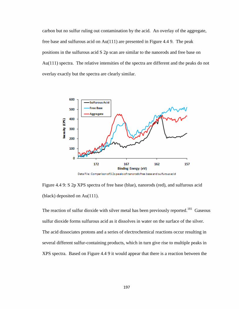
197
carbon but no sulfur ruling out contamination by the acid. An overlay of the aggregate,
free base and sulfurous acid on Au(111) are presented in Figure 4.4 9. The peak
positions in the sulfurous acid S 2p scan are similar to the nanorods and free base on
Au(111) spectra. The relative intensities of the spectra are different and the peaks do not
overlay exactly but the spectra are clearly similar.
Figure 4.4 9: S 2p XPS spectra of free base (blue), nanorods (red), and sulfurous acid
(black) deposited on Au(111).
The reaction of sulfur dioxide with silver metal has been previously reported.181
Gaseous
sulfur dioxide forms sulfurous acid as it dissolves in water on the surface of the silver.
The acid dissociates protons and a series of electrochemical reactions occur resulting in
several different sulfur-containing products, which in turn give rise to multiple peaks in
XPS spectra. Based on Figure 4.4 9 it would appear that there is a reaction between the
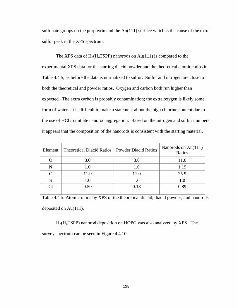
198
sulfonate groups on the porphyrin and the Au(111) surface which is the cause of the extra
sulfur peak in the XPS spectrum.
The XPS data of H2(H4TSPP) nanorods on Au(111) is compared to the
experimental XPS data for the starting diacid powder and the theoretical atomic ratios in
Table 4.4 5; as before the data is normalized to sulfur. Sulfur and nitrogen are close to
both the theoretical and powder ratios. Oxygen and carbon both run higher than
expected. The extra carbon is probably contamination; the extra oxygen is likely some
form of water. It is difficult to make a statement about the high chlorine content due to
the use of HCl to initiate nanorod aggregation. Based on the nitrogen and sulfur numbers
it appears that the composition of the nanorods is consistent with the starting material.
Element Theoretical Diacid Ratios Powder Diacid Ratios Nanorods on Au(111)
Ratios
O 3.0 3.8 11.6
N 1.0 1.0 1.19
C 11.0 11.0 25.9
S 1.0 1.0 1.0
Cl 0.50 0.18 0.89
Table 4.4 5: Atomic ratios by XPS of the theoretical diacid, diacid powder, and nanorods
deposited on Au(111).
H2(H4TSPP) nanorod deposition on HOPG was also analyzed by XPS. The
survey spectrum can be seen in Figure 4.4 10.
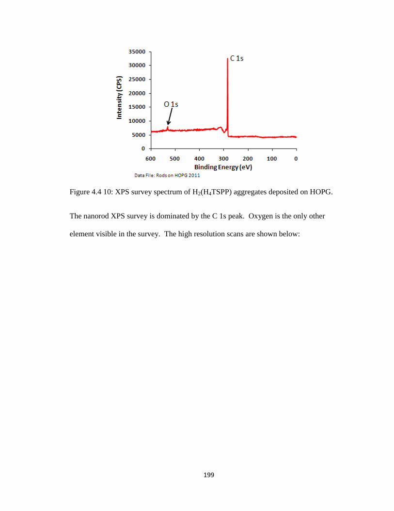
199
Figure 4.4 10: XPS survey spectrum of H2(H4TSPP) aggregates deposited on HOPG.
The nanorod XPS survey is dominated by the C 1s peak. Oxygen is the only other
element visible in the survey. The high resolution scans are shown below:
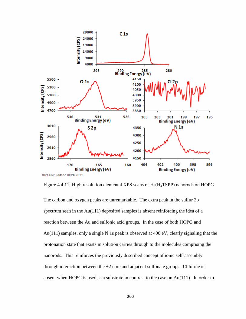
200
Figure 4.4 11: High resolution elemental XPS scans of H2(H4TSPP) nanorods on HOPG.
The carbon and oxygen peaks are unremarkable. The extra peak in the sulfur 2p
spectrum seen in the Au(111) deposited samples is absent reinforcing the idea of a
reaction between the Au and sulfonic acid groups. In the case of both HOPG and
Au(111) samples, only a single N 1s peak is observed at 400 eV, clearly signaling that the
protonation state that exists in solution carries through to the molecules comprising the
nanorods. This reinforces the previously described concept of ionic self-assembly
through interaction between the +2 core and adjacent sulfonate groups. Chlorine is
absent when HOPG is used as a substrate in contrast to the case on Au(111). In order to

201
better understand this, we performed XPS studies on clean substrates, substrates treated
with 0.75 M HCl, and those treated with 5 µM diacid in 0.75 M HCl. In the case of
HOPG, no chlorine was ever detected. In the case of Au(111) a clear chlorine peak of
about the same intensity was seen from either HCl only or diacid in HCl treated samples.
When these Au substrate samples were heated to 100C in UHV, the chlorine signal
disappeared. We interpret these results to mean that the Au is reacting with HCl to form
a thin surface chloride layer that can be decomposed on heating.
Similarly to the nanorod on Au(111) case XPS data of H2(H4TSPP) nanorods on
HOPG is compared to the experimental XPS data for the starting diacid powder and the
theoretical atomic ratios in Table 4.4 5; as before the data is normalized to sulfur. Sulfur
and nitrogen are close to both the theoretical and powder ratios. Oxygen and carbon both
run higher than expected. The extra carbon is not surprising considering the graphite
substrate. The extra oxygen is likely some form of water; it is interesting that there is
much less water in the HOPG sample than on Au(111). Based on the nitrogen and sulfur
numbers it appears that the composition of the nanorods is consistent with the starting
material.
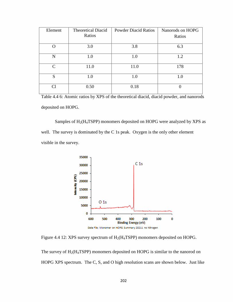
202
Element Theoretical Diacid
Ratios
Powder Diacid Ratios Nanorods on HOPG
Ratios
O 3.0 3.8 6.3
N 1.0 1.0 1.2
C 11.0 11.0 178
S 1.0 1.0 1.0
Cl 0.50 0.18 0
Table 4.4 6: Atomic ratios by XPS of the theoretical diacid, diacid powder, and nanorods
deposited on HOPG.
Samples of H2(H4TSPP) monomers deposited on HOPG were analyzed by XPS as
well. The survey is dominated by the C 1s peak. Oxygen is the only other element
visible in the survey.
Figure 4.4 12: XPS survey spectrum of H2(H4TSPP) monomers deposited on HOPG.
The survey of H2(H4TSPP) monomers deposited on HOPG is similar to the nanorod on
HOPG XPS spectrum. The C, S, and O high resolution scans are shown below. Just like
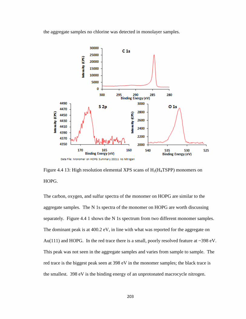
203
the aggregate samples no chlorine was detected in monolayer samples.
Figure 4.4 13: High resolution elemental XPS scans of H2(H4TSPP) monomers on
HOPG.
The carbon, oxygen, and sulfur spectra of the monomer on HOPG are similar to the
aggregate samples. The N 1s spectra of the monomer on HOPG are worth discussing
separately. Figure 4.4 1 shows the N 1s spectrum from two different monomer samples.
The dominant peak is at 400.2 eV, in line with what was reported for the aggregate on
Au(111) and HOPG. In the red trace there is a small, poorly resolved feature at ~398 eV.
This peak was not seen in the aggregate samples and varies from sample to sample. The
red trace is the biggest peak seen at 398 eV in the monomer samples; the black trace is
the smallest. 398 eV is the binding energy of an unprotonated macrocycle nitrogen.
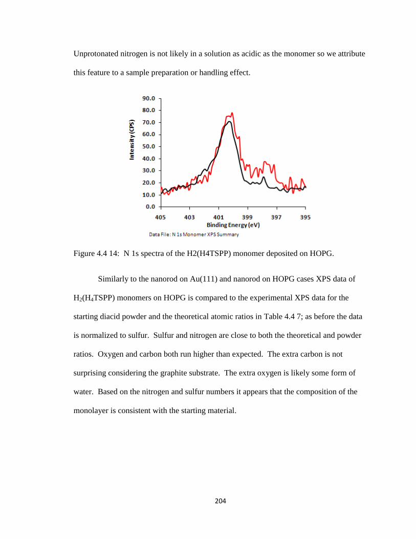
204
Unprotonated nitrogen is not likely in a solution as acidic as the monomer so we attribute
this feature to a sample preparation or handling effect.
Figure 4.4 14: N 1s spectra of the H2(H4TSPP) monomer deposited on HOPG.
Similarly to the nanorod on Au(111) and nanorod on HOPG cases XPS data of
H2(H4TSPP) monomers on HOPG is compared to the experimental XPS data for the
starting diacid powder and the theoretical atomic ratios in Table 4.4 7; as before the data
is normalized to sulfur. Sulfur and nitrogen are close to both the theoretical and powder
ratios. Oxygen and carbon both run higher than expected. The extra carbon is not
surprising considering the graphite substrate. The extra oxygen is likely some form of
water. Based on the nitrogen and sulfur numbers it appears that the composition of the
monolayer is consistent with the starting material.
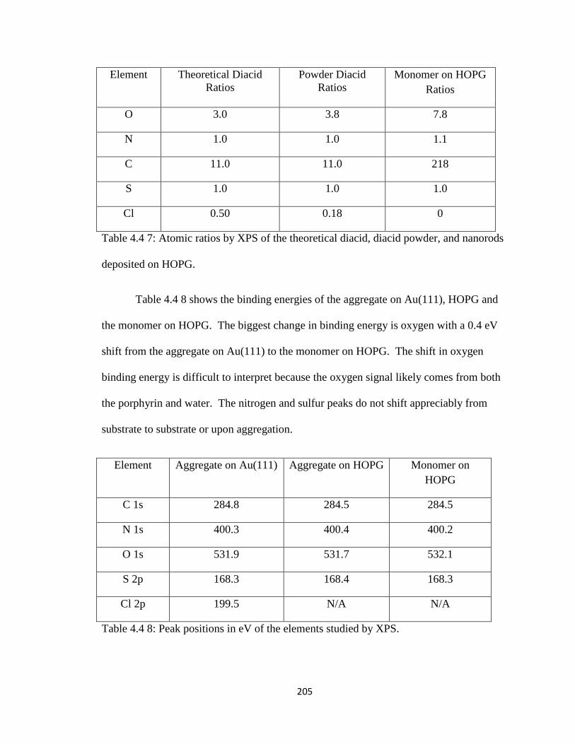
205
Element Theoretical Diacid
Ratios
Powder Diacid
Ratios
Monomer on HOPG
Ratios
O 3.0 3.8 7.8
N 1.0 1.0 1.1
C 11.0 11.0 218
S 1.0 1.0 1.0
Cl 0.50 0.18 0
Table 4.4 7: Atomic ratios by XPS of the theoretical diacid, diacid powder, and nanorods
deposited on HOPG.
Table 4.4 8 shows the binding energies of the aggregate on Au(111), HOPG and
the monomer on HOPG. The biggest change in binding energy is oxygen with a 0.4 eV
shift from the aggregate on Au(111) to the monomer on HOPG. The shift in oxygen
binding energy is difficult to interpret because the oxygen signal likely comes from both
the porphyrin and water. The nitrogen and sulfur peaks do not shift appreciably from
substrate to substrate or upon aggregation.
Element Aggregate on Au(111) Aggregate on HOPG Monomer on
HOPG
C 1s 284.8 284.5 284.5
N 1s 400.3 400.4 400.2
O 1s 531.9 531.7 532.1
S 2p 168.3 168.4 168.3
Cl 2p 199.5 N/A N/A
Table 4.4 8: Peak positions in eV of the elements studied by XPS.
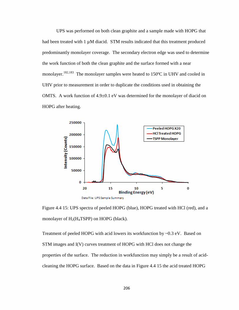
206
UPS was performed on both clean graphite and a sample made with HOPG that
had been treated with 1 µM diacid. STM results indicated that this treatment produced
predominantly monolayer coverage. The secondary electron edge was used to determine
the work function of both the clean graphite and the surface formed with a near
monolayer.182,183
The monolayer samples were heated to 150ºC in UHV and cooled in
UHV prior to measurement in order to duplicate the conditions used in obtaining the
OMTS. A work function of 4.9±0.1 eV was determined for the monolayer of diacid on
HOPG after heating.
Figure 4.4 15: UPS spectra of peeled HOPG (blue), HOPG treated with HCl (red), and a
monolayer of H2(H4TSPP) on HOPG (black).
Treatment of peeled HOPG with acid lowers its workfunction by ~0.3 eV. Based on
STM images and I(V) curves treatment of HOPG with HCl does not change the
properties of the surface. The reduction in workfunction may simply be a result of acid-
cleaning the HOPG surface. Based on the data in Figure 4.4 15 the acid treated HOPG
207
and the monolayer sample have the same workfunction (within 0.2 eV). This suggests
that monolayer deposition has very little effect on workfunction.
4.5 Ultra-High Vacuum STM Studies of H2(H4TSPP) Nanorods
4.5.1 UHV-STM Imaging Studies of H2(H4TSPP) Nanorods
While there are several proposed structures for the rods that are consistent with an
ionic self-assembly pattern,50,61
there is no general agreement on exactly how the
molecules form the observed rods. It should be noted that there is good evidence that
these “rods” are actually collapsed nanotubes. For example, as was mentioned in the
literature review Vlaming and coworkers have recently shown Cryo-EM images of these
nanostructures in frozen solution that are clearly tubes of 18 nm diameter with walls ~2
nm thick.61
In some of our STM images, we have also seen evidence that the 4 nm thick
rods are actually collapsed tubes having 2 nm thick walls. Typical large UHV-STM
images of nanorod sections on both Au(111) and HOPG are presented in Figure 4.5.1 1.
All samples were heated to 100°C prior to imaging.
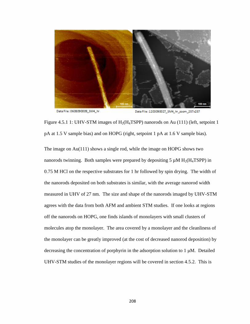
208
Figure 4.5.1 1: UHV-STM images of H2(H4TSPP) nanorods on Au (111) (left, setpoint 1
pA at 1.5 V sample bias) and on HOPG (right, setpoint 1 pA at 1.6 V sample bias).
The image on Au(111) shows a single rod, while the image on HOPG shows two
nanorods twinning. Both samples were prepared by depositing 5 µM H2(H4TSPP) in
0.75 M HCl on the respective substrates for 1 hr followed by spin drying. The width of
the nanorods deposited on both substrates is similar, with the average nanorod width
measured in UHV of 27 nm. The size and shape of the nanorods imaged by UHV-STM
agrees with the data from both AFM and ambient STM studies. If one looks at regions
off the nanorods on HOPG, one finds islands of monolayers with small clusters of
molecules atop the monolayer. The area covered by a monolayer and the cleanliness of
the monolayer can be greatly improved (at the cost of decreased nanorod deposition) by
decreasing the concentration of porphyrin in the adsorption solution to 1 μM. Detailed
UHV-STM studies of the monolayer regions will be covered in section 4.5.2. This is
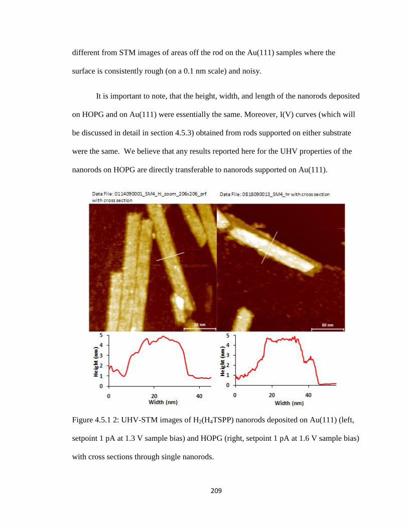
209
different from STM images of areas off the rod on the Au(111) samples where the
surface is consistently rough (on a 0.1 nm scale) and noisy.
It is important to note, that the height, width, and length of the nanorods deposited
on HOPG and on Au(111) were essentially the same. Moreover, I(V) curves (which will
be discussed in detail in section 4.5.3) obtained from rods supported on either substrate
were the same. We believe that any results reported here for the UHV properties of the
nanorods on HOPG are directly transferable to nanorods supported on Au(111).
Figure 4.5.1 2: UHV-STM images of H2(H4TSPP) nanorods deposited on Au(111) (left,
setpoint 1 pA at 1.3 V sample bias) and HOPG (right, setpoint 1 pA at 1.6 V sample bias)
with cross sections through single nanorods.

210
Both cross sections in Figure 4.5.1 2 show nanorods ~ 30 nm wide and ~ 4 nm
tall. As indicated earlier, the “rods” appear to be collapsed nanotubes having a wall
thickness of 2 nm which is well illustrated in the cross section of the nanorod on HOPG.
The cross sectional trace and image clearly show a layered structure to the nanorod. The
nanorod on HOPG is lying on the boundary of a monomer island and bare HOPG. This
can be seen in the cross section as the background height is different on the two sides of
the nanorod. The rod is 4 nm tall measured from the monolayer side and 4.5 nm tall
measured from the bare HOPG side. The extra 0.5 nm is most likely due to the rod lying
on top of the monolayer.
So far AFM and STM studies have proven futile in resolving the question of
precise nanorod structure. Figure 4.5.1 3 shows a relatively small scale STM image of a
nanorod and a region of monomers. While no internal molecular structure can be seen in
the aggregate individual molecules are resolved as well as individual molecular vacancies
are observed in the monolayer. Extra molecules and smaller aggregates, possibly dimers
or trimers, can be seen on top of the monolayer as well.
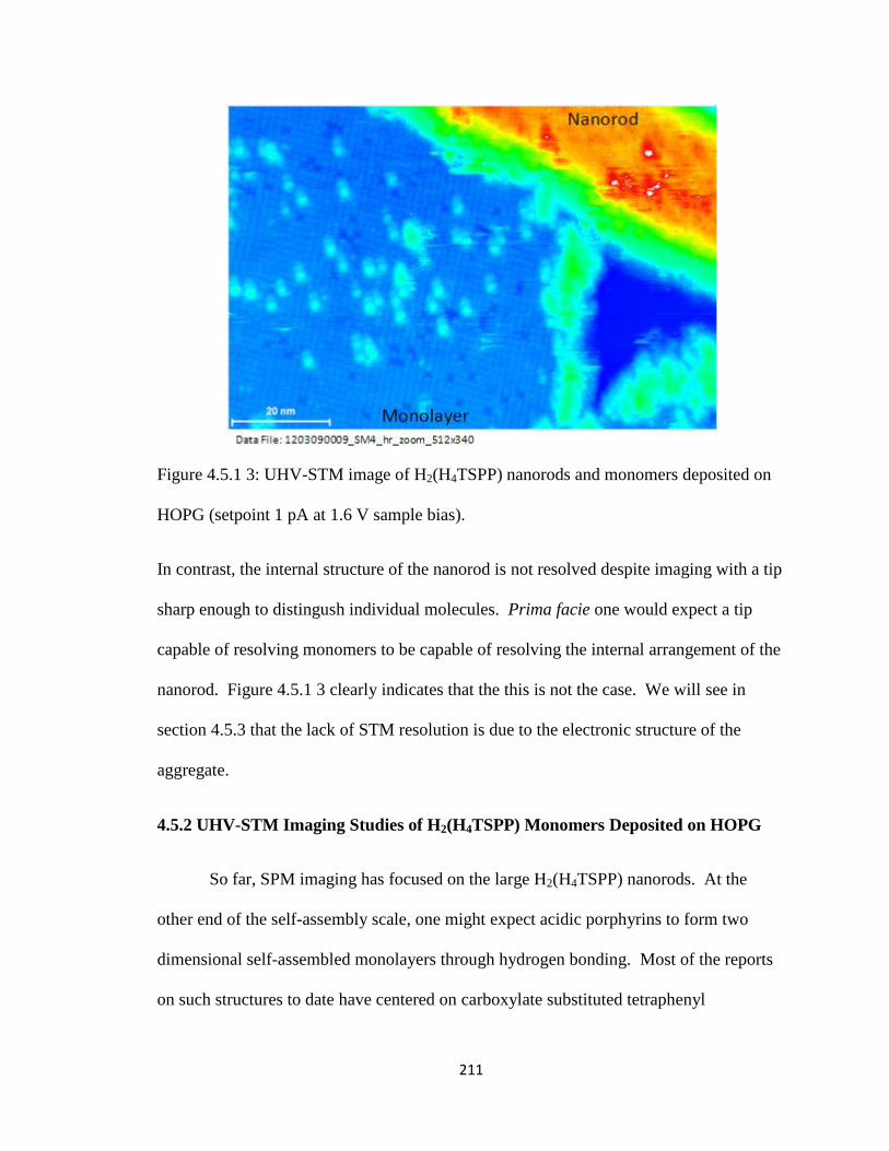
211
Figure 4.5.1 3: UHV-STM image of H2(H4TSPP) nanorods and monomers deposited on
HOPG (setpoint 1 pA at 1.6 V sample bias).
In contrast, the internal structure of the nanorod is not resolved despite imaging with a tip
sharp enough to distingush individual molecules. Prima facie one would expect a tip
capable of resolving monomers to be capable of resolving the internal arrangement of the
nanorod. Figure 4.5.1 3 clearly indicates that the this is not the case. We will see in
section 4.5.3 that the lack of STM resolution is due to the electronic structure of the
aggregate.
4.5.2 UHV-STM Imaging Studies of H2(H4TSPP) Monomers Deposited on HOPG
So far, SPM imaging has focused on the large H2(H4TSPP) nanorods. At the
other end of the self-assembly scale, one might expect acidic porphyrins to form two
dimensional self-assembled monolayers through hydrogen bonding. Most of the reports
on such structures to date have centered on carboxylate substituted tetraphenyl
212
porphyrins. Species with one to four carboxylates (CmTPP, m=1-4; the m=4 species is
commonly referred to as TCPP, have been investigated by scanning tunneling
microscopy (STM) on Au(111)184-188
and on HOPG.189,190
While CmTPP can be imaged
on Au(111) in either UHV or in the electrochemical environment, it cannot be observed
on HOPG unless a second species is used to reduce the mobility of the porphyrin on the
HOPG surface. Nicholls and coworkers used a buffer layer of 5-(octyldecyloxy)
isophthalic acid (a monolayer on HOPG) to reduce the mobility of CuTCPP to the point
where a structured adlayer could be observed.189
In this case, a very open square
structure with a molecular lattice having a spacing of 2.5 nm results from end-on H-
bonding between CuC4TPP molecules. Lei et al. coadsorbed TCPP with steric acid in
order to get a dried, mixed adlayer in which islands of TCPP could be imaged by STM.
They report two different structures, one with direct-on H-bonding having a 2.3 nm
lattice spacing, and a higher density square structure with a 1.8 nm lattice constant where
there is a more communal H-bonding between four carboxylates. It is not clear from
Lei‟s data whether the steric acid adlayer merely compresses the TCPP, or if the TCPP
adds on top of it as in the isophthalic acid case. Another oddity of most of these papers is
that the protonation state of the pyrrole nitrogens is not considered. Borguet appears to
be the only author who seriously includes this complication.184
The pKa values of the
pyrrole nitrogens and of the carboxylates in TCPP are close to 5.59
Thus, it is extremely
difficult to protonate the carboxylates without protonating all the central nitrogens,
thereby producing a zwitterionic species. In this section we will report on the monolayer
coverage of H2(H4TSPP) on HOPG. We will show that the structure and electronic
properties of this system are significantly different than the carboxylate analog.
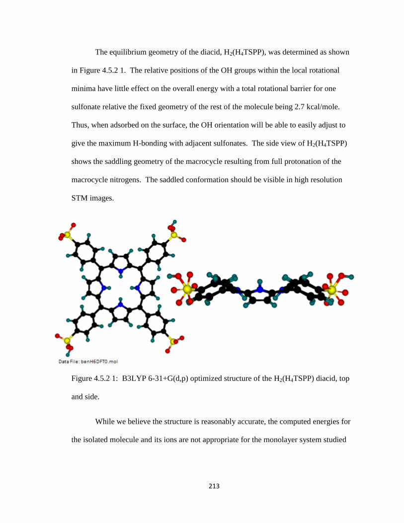
213
The equilibrium geometry of the diacid, H2(H4TSPP), was determined as shown
in Figure 4.5.2 1. The relative positions of the OH groups within the local rotational
minima have little effect on the overall energy with a total rotational barrier for one
sulfonate relative the fixed geometry of the rest of the molecule being 2.7 kcal/mole.
Thus, when adsorbed on the surface, the OH orientation will be able to easily adjust to
give the maximum H-bonding with adjacent sulfonates. The side view of H2(H4TSPP)
shows the saddling geometry of the macrocycle resulting from full protonation of the
macrocycle nitrogens. The saddled conformation should be visible in high resolution
STM images.
Figure 4.5.2 1: B3LYP 6-31+G(d,p) optimized structure of the H2(H4TSPP) diacid, top
and side.
While we believe the structure is reasonably accurate, the computed energies for
the isolated molecule and its ions are not appropriate for the monolayer system studied
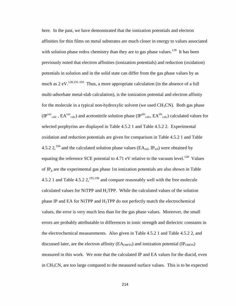
214
here. In the past, we have demonstrated that the ionization potentials and electron
affinities for thin films on metal substrates are much closer in energy to values associated
with solution phase redox chemistry than they are to gas phase values.128
It has been
previously noted that electron affinities (ionization potentials) and reduction (oxidation)
potentials in solution and in the solid state can differ from the gas phase values by as
much as 2 eV.128,191-193
Thus, a more appropriate calculation (in the absence of a full
multi-adsorbate metal-slab calculation), is the ionization potential and electron affinity
for the molecule in a typical non-hydroxylic solvent (we used CH3CN). Both gas phase
(IPvac
calc , EAvac
calc) and acetonitrile solution phase (IPsln
calc, EAsln
calc) calculated values for
selected porphyrins are displayed in Table 4.5.2 1 and Table 4.5.2 2. Experimental
oxidation and reduction potentials are given for comparison in Table 4.5.2 1 and Table
4.5.2 2,194
and the calculated solution phase values (EAsol, IPsol) were obtained by
equating the reference SCE potential to 4.71 eV relative to the vacuum level.128
Values
of IPg are the experimental gas phase 1st ionization potentials are also shown in Table
4.5.2 1 and Table 4.5.2 2,195,196
and compare reasonably well with the free molecule
calculated values for NiTPP and H2TPP. While the calculated values of the solution
phase IP and EA for NiTPP and H2TPP do not perfectly match the electrochemical
values, the error is very much less than for the gas phase values. Moreover, the small
errors are probably attributable to differences in ionic strength and dielectric constants in
the electrochemical measurements. Also given in Table 4.5.2 1 and Table 4.5.2 2, and
discussed later, are the electron affinity (EAOMTS) and ionization potential (IPOMTS)
measured in this work. We note that the calculated IP and EA values for the diacid, even
in CH3CN, are too large compared to the measured surface values. This is to be expected
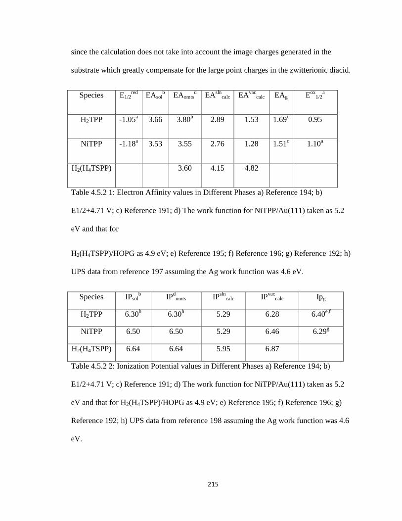
215
since the calculation does not take into account the image charges generated in the
substrate which greatly compensate for the large point charges in the zwitterionic diacid.
Species E1/2red
EAsolb EAomts
d EA
slncalc EA
vaccalc EAg E
ox1/2
a
H2TPP -1.05a 3.66 3.80
h 2.89 1.53 1.69
c 0.95
NiTPP -1.18a 3.53 3.55 2.76 1.28 1.51
c 1.10
a
H2(H4TSPP) 3.60 4.15 4.82
Table 4.5.2 1: Electron Affinity values in Different Phases a) Reference 194; b)
E1/2+4.71 V; c) Reference 191; d) The work function for NiTPP/Au(111) taken as 5.2
eV and that for
H2(H4TSPP)/HOPG as 4.9 eV; e) Reference 195; f) Reference 196; g) Reference 192; h)
UPS data from reference 197 assuming the Ag work function was 4.6 eV.
Species IPsolb IP
domts IP
slncalc IP
vaccalc Ipg
H2TPP 6.30h 6.30
h 5.29 6.28 6.40
e,f
NiTPP 6.50 6.50 5.29 6.46 6.29g
H2(H4TSPP) 6.64 6.64 5.95 6.87
Table 4.5.2 2: Ionization Potential values in Different Phases a) Reference 194; b)
E1/2+4.71 V; c) Reference 191; d) The work function for NiTPP/Au(111) taken as 5.2
eV and that for H2(H4TSPP)/HOPG as 4.9 eV; e) Reference 195; f) Reference 196; g)
Reference 192; h) UPS data from reference 198 assuming the Ag work function was 4.6
eV.
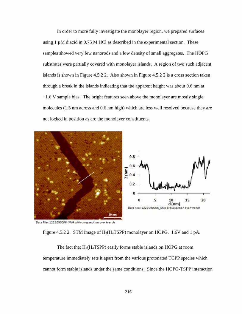
216
In order to more fully investigate the monolayer region, we prepared surfaces
using 1 µM diacid in 0.75 M HCl as described in the experimental section. These
samples showed very few nanorods and a low density of small aggregates. The HOPG
substrates were partially covered with monolayer islands. A region of two such adjacent
islands is shown in Figure 4.5.2 2. Also shown in Figure 4.5.2 2 is a cross section taken
through a break in the islands indicating that the apparent height was about 0.6 nm at
+1.6 V sample bias. The bright features seen above the monolayer are mostly single
molecules (1.5 nm across and 0.6 nm high) which are less well resolved because they are
not locked in position as are the monolayer constituents.
Figure 4.5.2 2: STM image of H2(H4TSPP) monolayer on HOPG. 1.6V and 1 pA.
The fact that H2(H4TSPP) easily forms stable islands on HOPG at room
temperature immediately sets it apart from the various protonated TCPP species which
cannot form stable islands under the same conditions. Since the HOPG-TSPP interaction
217
should be similar to the HOPG-TCPP interaction, one immediately suspects a difference
in the hydrogen bonding between TSPP molecules and that between TCPP molecules.
The only problem here is the issue of whether the protonation state of the nitrogens is the
same as the diacid in the previous studies. Few of these studies of TCPP have clearly
recognized the possibility of protonation of the nitrogens. While the carboxylates are
significantly more basic than the sulfonates, and therefore protonate first, the inner
nitrogens are all expected to be protonated at pH less than about 4.199
At pH below 4, the
inner ring is therefore expected to be highly positively charged for both TCPP and TSPP.
Since the electrochemical studies on TCPP were carried out in acid solution, it is likely
that they involved the inner protonated species. Borguet appears to be the only
investigator to clearly understand this and his model for the electrochemical process
explicitly involves the nitrogen protonation.184
One is left with two possibilities. 1) Both
TCPP and TSPP had completely protonated nitrogens and it is solely the difference in
hydrogen bonding that causes TSPP to order on HOPG; or 2) In previous studies of
TCPP on HOPG the pH was such that only two of the nitrogen atoms were protonated.
In this case the role of image charges in stabilizing the zwitterionic diacid of TSPP may
play an equal or even greater role than the H bonding differences.
A high resolution image of the monolayer is shown in Figure 4.5.2 3. Note that
while the monolayer shows some order, it is defective. On closer examination one sees
that two types of individual molecular images are present. Some of the molecules appear
to be divided in half nearly vertically (see rectangle in Figure 4.5.2 3) and others are
divided in half at right angles to the first set (see oval in Figure 4.5.2 3). This central
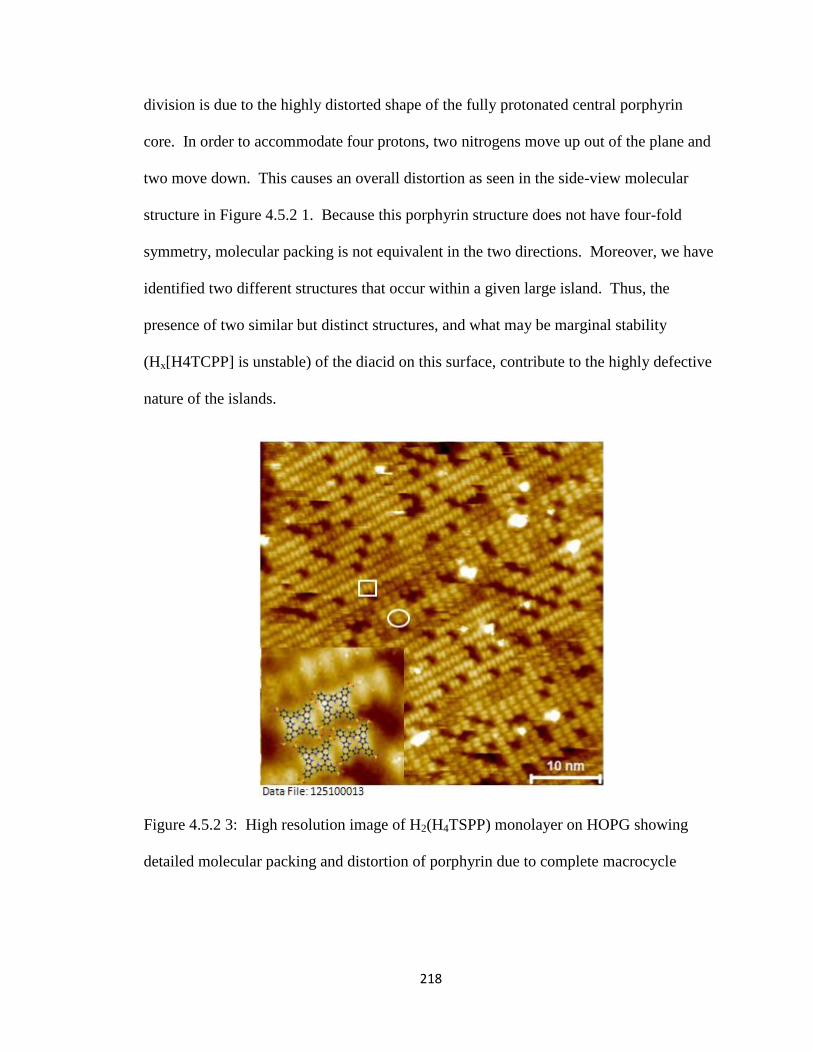
218
division is due to the highly distorted shape of the fully protonated central porphyrin
core. In order to accommodate four protons, two nitrogens move up out of the plane and
two move down. This causes an overall distortion as seen in the side-view molecular
structure in Figure 4.5.2 1. Because this porphyrin structure does not have four-fold
symmetry, molecular packing is not equivalent in the two directions. Moreover, we have
identified two different structures that occur within a given large island. Thus, the
presence of two similar but distinct structures, and what may be marginal stability
(Hx[H4TCPP] is unstable) of the diacid on this surface, contribute to the highly defective
nature of the islands.
Figure 4.5.2 3: High resolution image of H2(H4TSPP) monolayer on HOPG showing
detailed molecular packing and distortion of porphyrin due to complete macrocycle
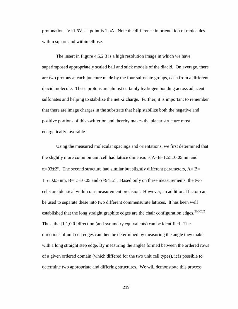
219
protonation. V=1.6V, setpoint is 1 pA. Note the difference in orientation of molecules
within square and within ellipse.
The insert in Figure 4.5.2 3 is a high resolution image in which we have
superimposed appropriately scaled ball and stick models of the diacid. On average, there
are two protons at each juncture made by the four sulfonate groups, each from a different
diacid molecule. These protons are almost certainly hydrogen bonding across adjacent
sulfonates and helping to stabilize the net -2 charge. Further, it is important to remember
that there are image charges in the substrate that help stabilize both the negative and
positive portions of this zwitterion and thereby makes the planar structure most
energetically favorable.
Using the measured molecular spacings and orientations, we first determined that
the slightly more common unit cell had lattice dimensions A=B=1.550.05 nm and
=932. The second structure had similar but slightly different parameters, A= B=
1.50.05 nm, B=1.50.05 and =942. Based only on these measurements, the two
cells are identical within our measurement precision. However, an additional factor can
be used to separate these into two different commensurate lattices. It has been well
established that the long straight graphite edges are the chair configuration edges.200-202
Thus, the [1,1,0,0] direction (and symmetry equivalents) can be identified. The
directions of unit cell edges can then be determined by measuring the angle they make
with a long straight step edge. By measuring the angles formed between the ordered rows
of a given ordered domain (which differed for the two unit cell types), it is possible to
determine two appropriate and differing structures. We will demonstrate this process
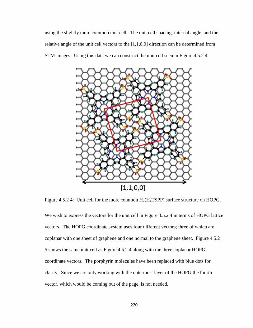
220
using the slightly more common unit cell. The unit cell spacing, internal angle, and the
relative angle of the unit cell vectors to the [1,1,0,0] direction can be determined from
STM images. Using this data we can construct the unit cell seen in Figure 4.5.2 4.
Figure 4.5.2 4: Unit cell for the more common H2(H4TSPP) surface structure on HOPG.
We wish to express the vectors for the unit cell in Figure 4.5.2 4 in terms of HOPG lattice
vectors. The HOPG coordinate system uses four different vectors; three of which are
coplanar with one sheet of graphene and one normal to the graphene sheet. Figure 4.5.2
5 shows the same unit cell as Figure 4.5.2 4 along with the three coplanar HOPG
coordinate vectors. The porphyrin molecules have been replaced with blue dots for
clarity. Since we are only working with the outermost layer of the HOPG the fourth
vector, which would be coming out of the page, is not needed.
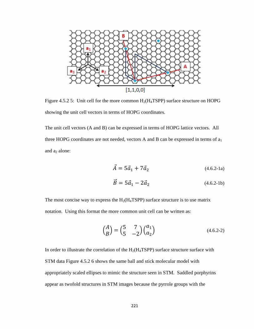
221
Figure 4.5.2 5: Unit cell for the more common H2(H4TSPP) surface structure on HOPG
showing the unit cell vectors in terms of HOPG coordinates.
The unit cell vectors (A and B) can be expressed in terms of HOPG lattice vectors. All
three HOPG coordinates are not needed, vectors A and B can be expressed in terms of a1
and a2 alone:
(4.6.2-1a)
(4.6.2-1b)
The most concise way to express the H2(H4TSPP) surface structure is to use matrix
notation. Using this format the more common unit cell can be written as:
(4.6.2-2)
In order to illustrate the correlation of the H2(H4TSPP) surface structure surface with
STM data Figure 4.5.2 6 shows the same ball and stick molecular model with
appropriately scaled ellipses to mimic the structure seen in STM. Saddled porphyrins
appear as twofold structures in STM images because the pyrrole groups with the
222
nitrogens pointing toward the surface show high contrast.203
Figure 4.5.2 6: Unit cell for the more common H2(H4TSPP) surface structure on HOPG
with overlaid ellipses to show correlation with STM images.
The second lattice can be visualized as 2166 aaA
and 2143 aaB
. In both
cases, there are several symmetry related equivalents. This would preclude the phase
separation one might normally expect. The first lattice (Figure 4.6.2.6) has unit cell
parameters A=B=1.54 nm and =92.2. The second proposed commensurate unit cell is
slightly smaller with A=1.48 nm, B=1.50 nm, and =94.7.
223
Figure 4.5.2 7: Unit cell for the less common H2(H4TSPP) surface structure on HOPG
with overlaid ellipses to show correlation with STM images.
The unit cells proposed here are much smaller than any proposed for TCPP in any
environment. The cells reported for TCPP to date are square cells with lattice vector 1.8
nm long,184,190
a hexagonal array with lattice constant near 1.7 nm,184
and very large cells
with lattice constants of the order of 2 nm and larger.187,189,190
Moreover, it has been
suggested that the phenyl groups lay flat on the surface in order to achieve the 1.8 nm
spacing,190
a situation that clearly does not occur for TSPP. The origin of the much
tighter structure and the non-parallel phenyl group orientations may be due to the near
tetrahedral nature of the sulfonate group. While a two carboxylates can only achieve full
H-bonding when directly aligned, the presence of three tetrahedrally coordinated oxygen
ions provide much more structural flexibility.
224
4.5.3 UHV-STM Current versus Voltage Studies of H2(H4TSPP) Nanorods and
Monomers
Current vs. voltage (I(V)) studies were carried out on nanorods deposited on
HOPG and Au(111) and on monomeric H2(H4TSPP) on HOPG. All measurements were
carried out with the vacuum system windows covered to eliminate photoinduced
reactions. Monomeric I(V) curves were not collected on Au(111) due to the surface
reaction with HCl, thus we will focus on I-V and OMTS data acquired from HOPG
supported samples that have been heated to 100°C. Tip cleanliness is of prime
importance when collecting I(V) so a particular protocol was followed in order to ensure
tip condition. First, as was described in section 2.4 tips were sputtered with argon ions to
remove the native oxide layer. After sputtering the tips were checked by scanning over a
Au(111) surface cleaned by repeated cycles of argon sputtering and annealing. A good
tip resolved the well-known Au(111) reconstruction and exhibited a linear I(V) curve. A
typical image of the Au(111) reconstruction and an accompanying I(V) curve are shown
in Figure 3.4 1. I(V) curves were collected over nanorods by taking an initial scan of ~
100 nm with a typical setpoint of 1 pA at 1.6 V sample bias. After the initial scan the tip
was positioned over the rod, the setpoint increased to 15 pA, and I(V) curves run. The
setpoint was increased after the tip was positioned over the nanorod because scanning at
higher setpoints disrupted the aggregates and contaminated the tips. Figure 4.5.3 1
presents I(V) curves of 4 nm tall nanorods deposited on Au(111) and on HOPG.
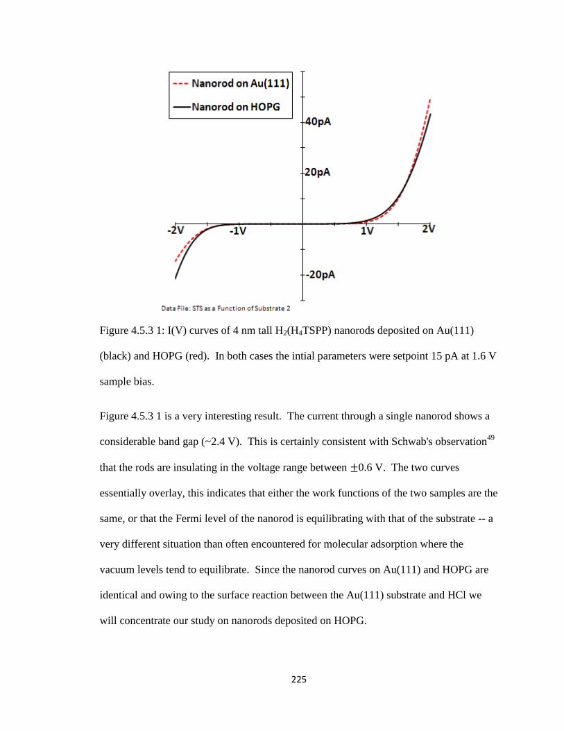
225
Figure 4.5.3 1: I(V) curves of 4 nm tall H2(H4TSPP) nanorods deposited on Au(111)
(black) and HOPG (red). In both cases the intial parameters were setpoint 15 pA at 1.6 V
sample bias.
Figure 4.5.3 1 is a very interesting result. The current through a single nanorod shows a
considerable band gap (~2.4 V). This is certainly consistent with Schwab's observation49
that the rods are insulating in the voltage range between 0.6 V. The two curves
essentially overlay, this indicates that either the work functions of the two samples are the
same, or that the Fermi level of the nanorod is equilibrating with that of the substrate -- a
very different situation than often encountered for molecular adsorption where the
vacuum levels tend to equilibrate. Since the nanorod curves on Au(111) and HOPG are
identical and owing to the surface reaction between the Au(111) substrate and HCl we
will concentrate our study on nanorods deposited on HOPG.
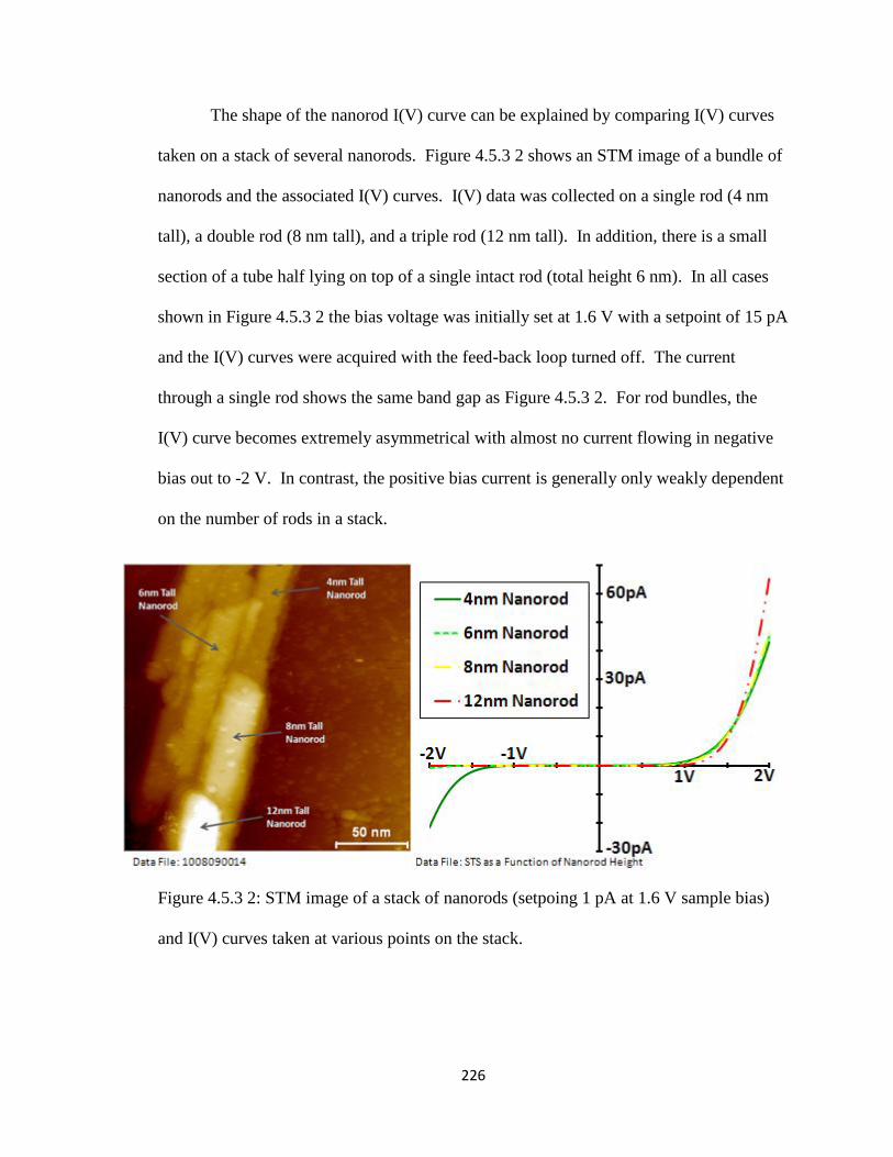
226
The shape of the nanorod I(V) curve can be explained by comparing I(V) curves
taken on a stack of several nanorods. Figure 4.5.3 2 shows an STM image of a bundle of
nanorods and the associated I(V) curves. I(V) data was collected on a single rod (4 nm
tall), a double rod (8 nm tall), and a triple rod (12 nm tall). In addition, there is a small
section of a tube half lying on top of a single intact rod (total height 6 nm). In all cases
shown in Figure 4.5.3 2 the bias voltage was initially set at 1.6 V with a setpoint of 15 pA
and the I(V) curves were acquired with the feed-back loop turned off. The current
through a single rod shows the same band gap as Figure 4.5.3 2. For rod bundles, the
I(V) curve becomes extremely asymmetrical with almost no current flowing in negative
bias out to -2 V. In contrast, the positive bias current is generally only weakly dependent
on the number of rods in a stack.
Figure 4.5.3 2: STM image of a stack of nanorods (setpoing 1 pA at 1.6 V sample bias)
and I(V) curves taken at various points on the stack.
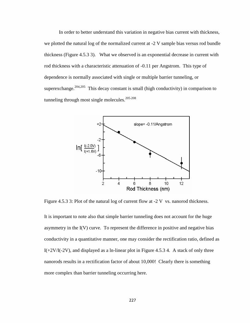
227
In order to better understand this variation in negative bias current with thickness,
we plotted the natural log of the normalized current at -2 V sample bias versus rod bundle
thickness (Figure 4.5.3 3). What we observed is an exponential decrease in current with
rod thickness with a characteristic attenuation of -0.11 per Angstrom. This type of
dependence is normally associated with single or multiple barrier tunneling, or
superexchange.204,205
This decay constant is small (high conductivity) in comparison to
tunneling through most single molecules.205-208
Figure 4.5.3 3: Plot of the natural log of current flow at -2 V vs. nanorod thickness.
It is important to note also that simple barrier tunneling does not account for the huge
asymmetry in the I(V) curve. To represent the difference in positive and negative bias
conductivity in a quantitative manner, one may consider the rectification ratio, defined as
I(+2V/I(-2V), and displayed as a ln-linear plot in Figure 4.5.3 4. A stack of only three
nanorods results in a rectification factor of about 10,000! Clearly there is something
more complex than barrier tunneling occurring here.
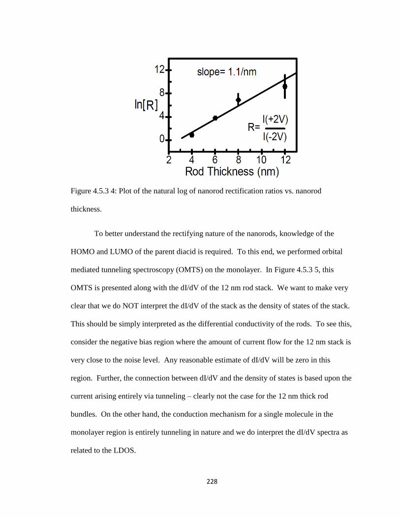
228
Figure 4.5.3 4: Plot of the natural log of nanorod rectification ratios vs. nanorod
thickness.
To better understand the rectifying nature of the nanorods, knowledge of the
HOMO and LUMO of the parent diacid is required. To this end, we performed orbital
mediated tunneling spectroscopy (OMTS) on the monolayer. In Figure 4.5.3 5, this
OMTS is presented along with the dI/dV of the 12 nm rod stack. We want to make very
clear that we do NOT interpret the dI/dV of the stack as the density of states of the stack.
This should be simply interpreted as the differential conductivity of the rods. To see this,
consider the negative bias region where the amount of current flow for the 12 nm stack is
very close to the noise level. Any reasonable estimate of dI/dV will be zero in this
region. Further, the connection between dI/dV and the density of states is based upon the
current arising entirely via tunneling – clearly not the case for the 12 nm thick rod
bundles. On the other hand, the conduction mechanism for a single molecule in the
monolayer region is entirely tunneling in nature and we do interpret the dI/dV spectra as
related to the LDOS.
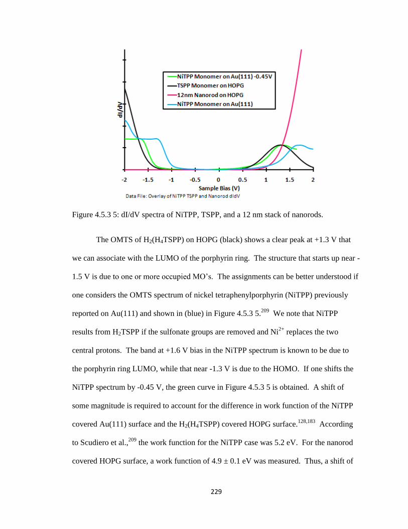
229
Figure 4.5.3 5: dI/dV spectra of NiTPP, TSPP, and a 12 nm stack of nanorods.
The OMTS of H2(H4TSPP) on HOPG (black) shows a clear peak at +1.3 V that
we can associate with the LUMO of the porphyrin ring. The structure that starts up near -
1.5 V is due to one or more occupied MO‟s. The assignments can be better understood if
one considers the OMTS spectrum of nickel tetraphenylporphyrin (NiTPP) previously
reported on Au(111) and shown in (blue) in Figure 4.5.3 5.209
We note that NiTPP
results from H2TSPP if the sulfonate groups are removed and Ni2+
replaces the two
central protons. The band at +1.6 V bias in the NiTPP spectrum is known to be due to
the porphyrin ring LUMO, while that near -1.3 V is due to the HOMO. If one shifts the
NiTPP spectrum by -0.45 V, the green curve in Figure 4.5.3 5 is obtained. A shift of
some magnitude is required to account for the difference in work function of the NiTPP
covered Au(111) surface and the H2(H4TSPP) covered HOPG surface.128,183
According
to Scudiero et al.,209
the work function for the NiTPP case was 5.2 eV. For the nanorod
covered HOPG surface, a work function of 4.9 ± 0.1 eV was measured. Thus, a shift of
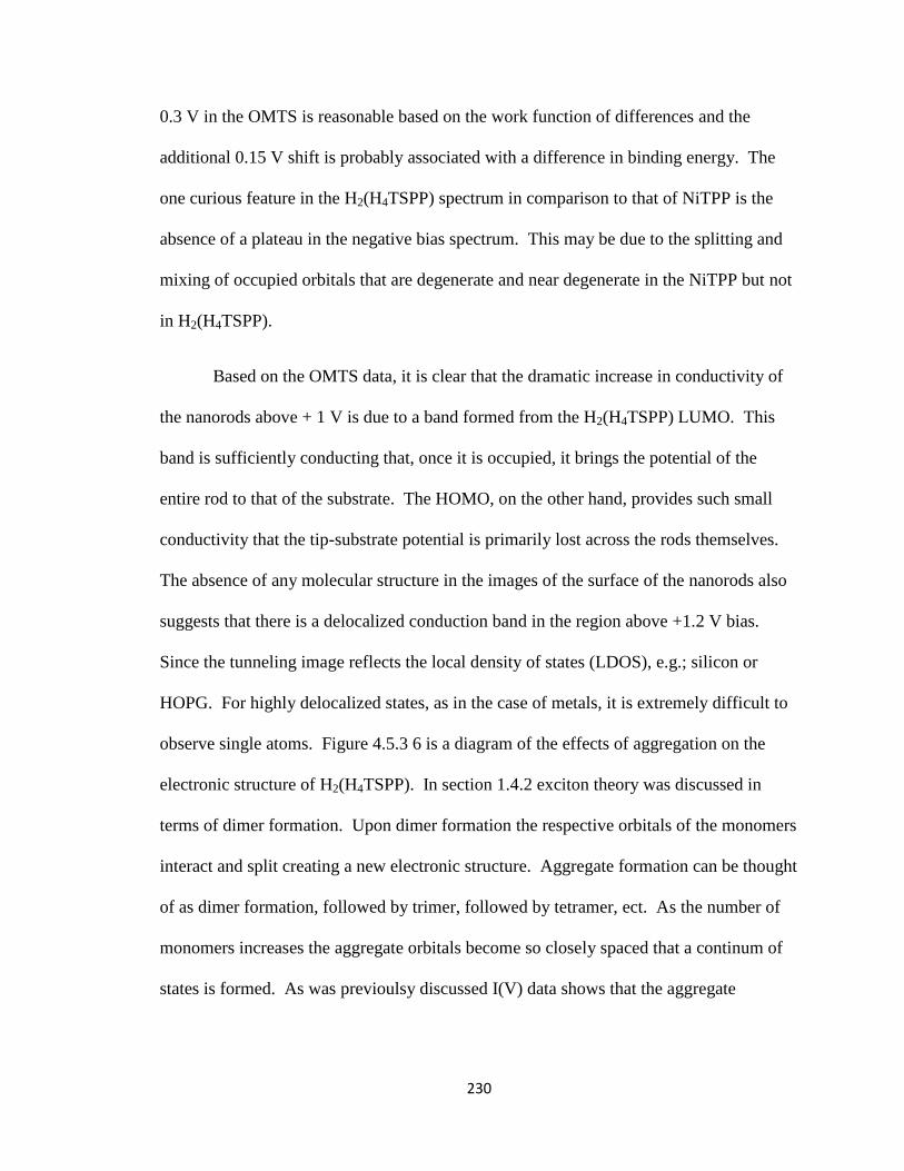
230
0.3 V in the OMTS is reasonable based on the work function of differences and the
additional 0.15 V shift is probably associated with a difference in binding energy. The
one curious feature in the H2(H4TSPP) spectrum in comparison to that of NiTPP is the
absence of a plateau in the negative bias spectrum. This may be due to the splitting and
mixing of occupied orbitals that are degenerate and near degenerate in the NiTPP but not
in H2(H4TSPP).
Based on the OMTS data, it is clear that the dramatic increase in conductivity of
the nanorods above + 1 V is due to a band formed from the H2(H4TSPP) LUMO. This
band is sufficiently conducting that, once it is occupied, it brings the potential of the
entire rod to that of the substrate. The HOMO, on the other hand, provides such small
conductivity that the tip-substrate potential is primarily lost across the rods themselves.
The absence of any molecular structure in the images of the surface of the nanorods also
suggests that there is a delocalized conduction band in the region above +1.2 V bias.
Since the tunneling image reflects the local density of states (LDOS), e.g.; silicon or
HOPG. For highly delocalized states, as in the case of metals, it is extremely difficult to
observe single atoms. Figure 4.5.3 6 is a diagram of the effects of aggregation on the
electronic structure of H2(H4TSPP). In section 1.4.2 exciton theory was discussed in
terms of dimer formation. Upon dimer formation the respective orbitals of the monomers
interact and split creating a new electronic structure. Aggregate formation can be thought
of as dimer formation, followed by trimer, followed by tetramer, ect. As the number of
monomers increases the aggregate orbitals become so closely spaced that a continum of
states is formed. As was previoulsy discussed I(V) data shows that the aggregate
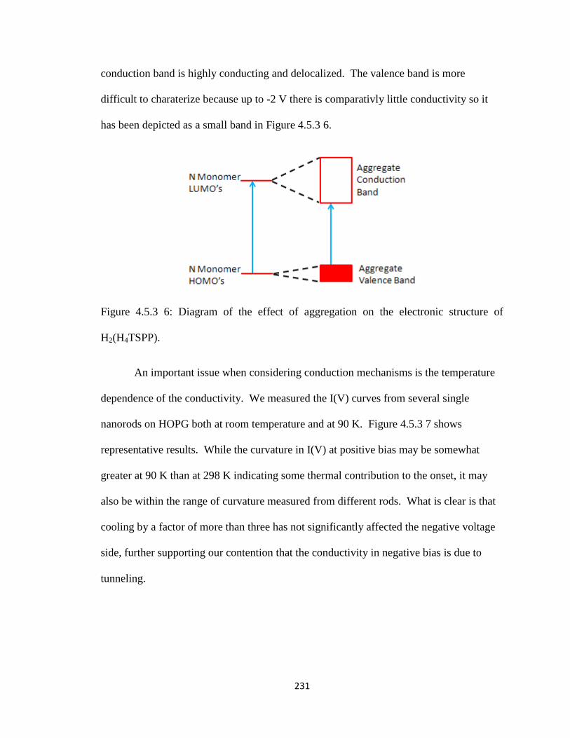
231
conduction band is highly conducting and delocalized. The valence band is more
difficult to charaterize because up to -2 V there is comparativly little conductivity so it
has been depicted as a small band in Figure 4.5.3 6.
Figure 4.5.3 6: Diagram of the effect of aggregation on the electronic structure of
H2(H4TSPP).
An important issue when considering conduction mechanisms is the temperature
dependence of the conductivity. We measured the I(V) curves from several single
nanorods on HOPG both at room temperature and at 90 K. Figure 4.5.3 7 shows
representative results. While the curvature in I(V) at positive bias may be somewhat
greater at 90 K than at 298 K indicating some thermal contribution to the onset, it may
also be within the range of curvature measured from different rods. What is clear is that
cooling by a factor of more than three has not significantly affected the negative voltage
side, further supporting our contention that the conductivity in negative bias is due to
tunneling.
232
Figure 4.5.3 7: I(V) curves of 4 nm nanorods taken at room temperature and 90 K.
4.6 Helium Ion Microscopy Studies
One of the major goals of this work is to resolve the molecular structure of
H2(H4TSPP) aggregates. To this end the nanorods were analyzed by HIM. Micrographs
were gathered for nanorods deposited on Au(111)/mica and peeled HOPG. The ORION®
He microscope is capable of imaging with two different detectors, an Everhart-Thornley
and a Rutherford backscattering detector. The Everhart-Thornley detector measures
secondary electrons ejected from the sample by the incident He ions, while the
Rutherford backscattering detector measures He ions scattered by the sample nuclei.135
Both modes were used to analyze the nanorods. The Rutherford backscattering technique
failed to show contrast between the nanorods and either substrate. The lack of contrast is
likely due to low backscattering yield from the light atoms in the nanorods as Rutherford
scattering increases with nuclear charge (Z).135
Figure 4.6 1 shows representative
micrographs of H2(H4TSPP) aggregates deposited on HOPG taken using the Everhart-
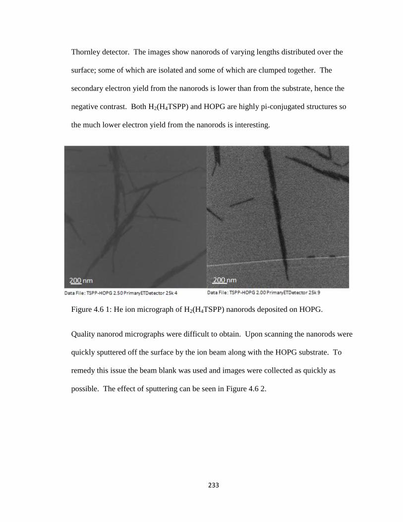
233
Thornley detector. The images show nanorods of varying lengths distributed over the
surface; some of which are isolated and some of which are clumped together. The
secondary electron yield from the nanorods is lower than from the substrate, hence the
negative contrast. Both H2(H4TSPP) and HOPG are highly pi-conjugated structures so
the much lower electron yield from the nanorods is interesting.
Figure 4.6 1: He ion micrograph of H2(H4TSPP) nanorods deposited on HOPG.
Quality nanorod micrographs were difficult to obtain. Upon scanning the nanorods were
quickly sputtered off the surface by the ion beam along with the HOPG substrate. To
remedy this issue the beam blank was used and images were collected as quickly as
possible. The effect of sputtering can be seen in Figure 4.6 2.
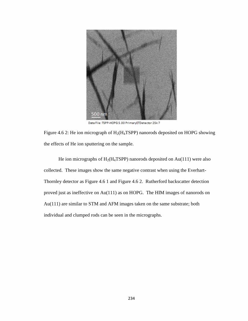
234
Figure 4.6 2: He ion micrograph of H2(H4TSPP) nanorods deposited on HOPG showing
the effects of He ion sputtering on the sample.
He ion micrographs of H2(H4TSPP) nanorods deposited on Au(111) were also
collected. These images show the same negative contrast when using the Everhart-
Thornley detector as Figure 4.6 1 and Figure 4.6 2. Rutherford backscatter detection
proved just as ineffective on Au(111) as on HOPG. The HIM images of nanorods on
Au(111) are similar to STM and AFM images taken on the same substrate; both
individual and clumped rods can be seen in the micrographs.
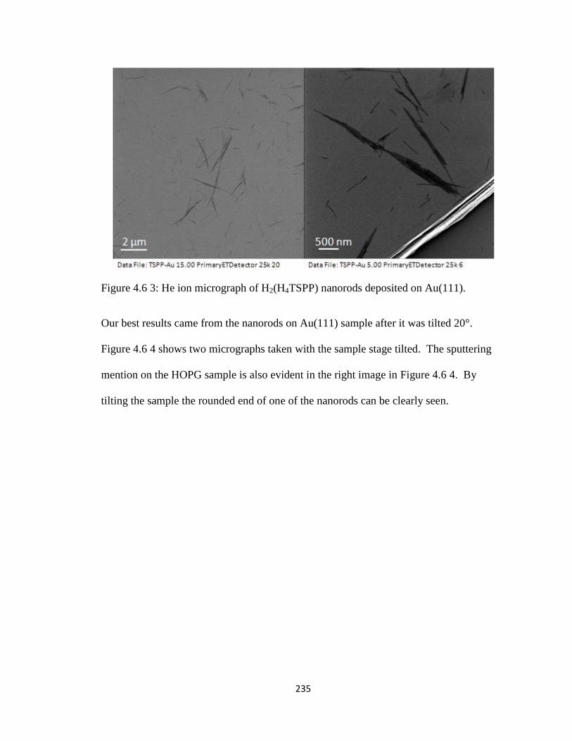
235
Figure 4.6 3: He ion micrograph of H2(H4TSPP) nanorods deposited on Au(111).
Our best results came from the nanorods on Au(111) sample after it was tilted 20°.
Figure 4.6 4 shows two micrographs taken with the sample stage tilted. The sputtering
mention on the HOPG sample is also evident in the right image in Figure 4.6 4. By
tilting the sample the rounded end of one of the nanorods can be clearly seen.
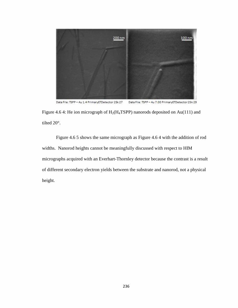
236
Figure 4.6 4: He ion micrograph of H2(H4TSPP) nanorods deposited on Au(111) and
tilted 20°.
Figure 4.6 5 shows the same micrograph as Figure 4.6 4 with the addition of rod
widths. Nanorod heights cannot be meaningfully discussed with respect to HIM
micrographs acquired with an Everhart-Thornley detector because the contrast is a result
of different secondary electron yields between the substrate and nanorod, not a physical
height.
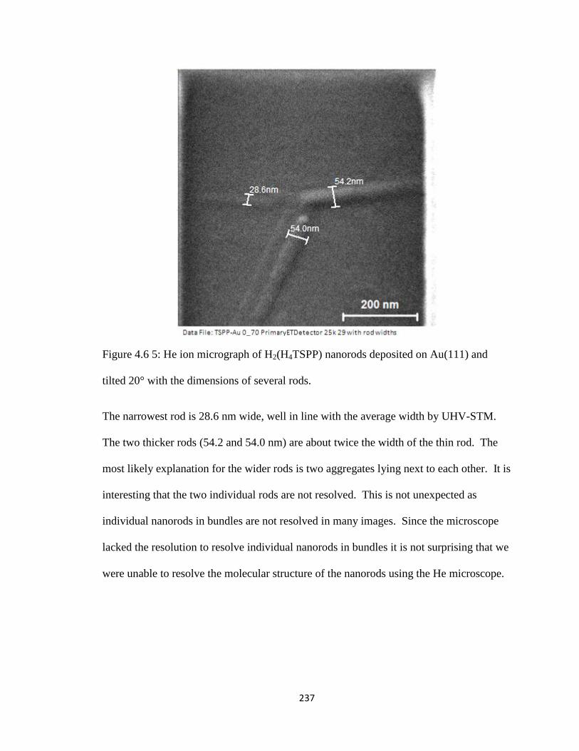
237
Figure 4.6 5: He ion micrograph of H2(H4TSPP) nanorods deposited on Au(111) and
tilted 20° with the dimensions of several rods.
The narrowest rod is 28.6 nm wide, well in line with the average width by UHV-STM.
The two thicker rods (54.2 and 54.0 nm) are about twice the width of the thin rod. The
most likely explanation for the wider rods is two aggregates lying next to each other. It is
interesting that the two individual rods are not resolved. This is not unexpected as
individual nanorods in bundles are not resolved in many images. Since the microscope
lacked the resolution to resolve individual nanorods in bundles it is not surprising that we
were unable to resolve the molecular structure of the nanorods using the He microscope.
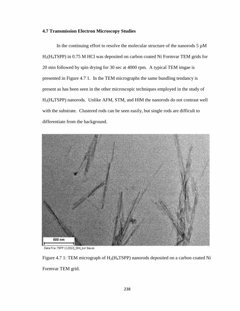
238
4.7 Transmission Electron Microscopy Studies
In the continuing effort to resolve the molecular structure of the nanorods 5 µM
H2(H4TSPP) in 0.75 M HCl was deposited on carbon coated Ni Formvar TEM grids for
20 min followed by spin drying for 30 sec at 4000 rpm. A typical TEM imgae is
presented in Figure 4.7 1. In the TEM micrographs the same bundling tendancy is
present as has been seen in the other microscopic techniques employed in the study of
H2(H4TSPP) nanorods. Unlike AFM, STM, and HIM the nanorods do not contrast well
with the substrate. Clustered rods can be seen easily, but single rods are difficult to
differentiate from the background.
Figure 4.7 1: TEM micrograph of H2(H4TSPP) nanorods deposited on a carbon coated Ni
Formvar TEM grid.
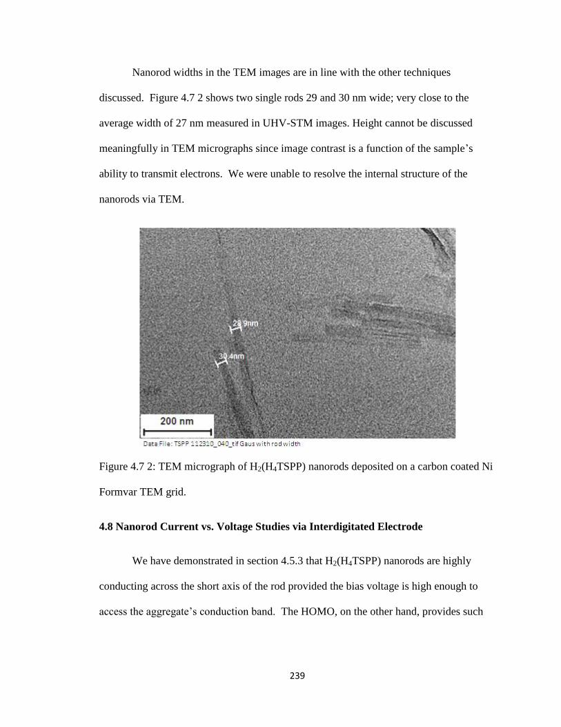
239
Nanorod widths in the TEM images are in line with the other techniques
discussed. Figure 4.7 2 shows two single rods 29 and 30 nm wide; very close to the
average width of 27 nm measured in UHV-STM images. Height cannot be discussed
meaningfully in TEM micrographs since image contrast is a function of the sample‟s
ability to transmit electrons. We were unable to resolve the internal structure of the
nanorods via TEM.
Figure 4.7 2: TEM micrograph of H2(H4TSPP) nanorods deposited on a carbon coated Ni
Formvar TEM grid.
4.8 Nanorod Current vs. Voltage Studies via Interdigitated Electrode
We have demonstrated in section 4.5.3 that H2(H4TSPP) nanorods are highly
conducting across the short axis of the rod provided the bias voltage is high enough to
access the aggregate‟s conduction band. The HOMO, on the other hand, provides such
240
small conductivity via a tunneling mechanism that the tip-substrate potential is primarily
lost across the rods themselves. The STM I(V) data presented relates to transverse
conduction in these nanorods. The effects of scattering centers, impurities, and physical
defects are minimized because of the very short path length. The role that imperfections
and transport direction plays in conduction is critical for any practical applications of this
intriguing material. We will address this question by running I(V) curves on nanorods
deposited on interdigitated gold electrodes. The electrode gap in the device is 400 nm as
measured by AFM so any rod conductivity observed will be in the longitudinal direction.
The experimental setup is covered in detail in the experimental section.
The construction of the electrode precludes AFM measurements after nanorod
deposition. In order to check nanorod surface coverage the IdE was imaged by SEM.
Figure 4.8 1 shows two SEM images of nanorods deposited on the IdE. As was the case
when the nanorods were imaged by HIM using secondary electron detection the rods
appear dark against the bright Au electrode.
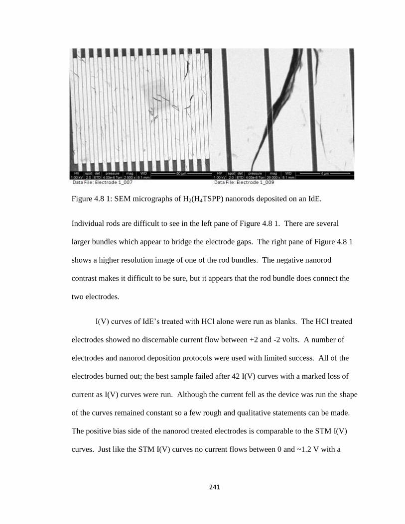
241
Figure 4.8 1: SEM micrographs of H2(H4TSPP) nanorods deposited on an IdE.
Individual rods are difficult to see in the left pane of Figure 4.8 1. There are several
larger bundles which appear to bridge the electrode gaps. The right pane of Figure 4.8 1
shows a higher resolution image of one of the rod bundles. The negative nanorod
contrast makes it difficult to be sure, but it appears that the rod bundle does connect the
two electrodes.
I(V) curves of IdE‟s treated with HCl alone were run as blanks. The HCl treated
electrodes showed no discernable current flow between +2 and -2 volts. A number of
electrodes and nanorod deposition protocols were used with limited success. All of the
electrodes burned out; the best sample failed after 42 I(V) curves with a marked loss of
current as I(V) curves were run. Although the current fell as the device was run the shape
of the curves remained constant so a few rough and qualitative statements can be made.
The positive bias side of the nanorod treated electrodes is comparable to the STM I(V)
curves. Just like the STM I(V) curves no current flows between 0 and ~1.2 V with a
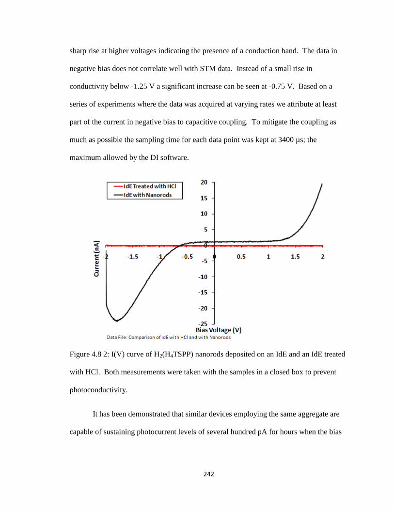
242
sharp rise at higher voltages indicating the presence of a conduction band. The data in
negative bias does not correlate well with STM data. Instead of a small rise in
conductivity below -1.25 V a significant increase can be seen at -0.75 V. Based on a
series of experiments where the data was acquired at varying rates we attribute at least
part of the current in negative bias to capacitive coupling. To mitigate the coupling as
much as possible the sampling time for each data point was kept at 3400 µs; the
maximum allowed by the DI software.
Figure 4.8 2: I(V) curve of H2(H4TSPP) nanorods deposited on an IdE and an IdE treated
with HCl. Both measurements were taken with the samples in a closed box to prevent
photoconductivity.
It has been demonstrated that similar devices employing the same aggregate are
capable of sustaining photocurrent levels of several hundred pA for hours when the bias
243
voltage is kept between ± 0.5 V.49,111
There are a number of possible explanations for the
instability of our samples. It may be that beyond ± 0.5 V the rods are unstable with
respect to longitudinal conduction which would account for the irreproducibility of our
results. There is one study of H2(H4TSPP) nanorod conductivity over ± 5 V which
showed an ohmic behavior.113
This study was different from ours in several important
ways. The device was very different in construction; nanorods were deposited on the
substrate followed by deposition of patterned Au metal on top of the aggregates. The
measurements were carried out in low vacuum (10-4
Torr); our data was gathered under
Ar. It was never stated whether or not the photoconductive nanorods were illuminated
during measurements. The differences in construction and experimental methodology
make comparison between the data problematic. A second explanation for irreproducible
results is the aforementioned capacitive coupling. I(V) measurements reported on a
similar device required a 1 hour wait between voltage changes for the current to
stabilize;49
our curves were taken in under one minute.
In summary we do not have good enough data to make firm conclusions regarding
conductivity down the long axis of H2(H4TSPP) nanorods. In order to obtain quality data
several issues must be addressed. First, the device should be redesigned so the electrodes
are at the same level as the substrate. Second, the issue of capacitive coupling must be
dealt with, possibly by taking data at a slower rate. Third, we must ascertain if the
devices are burning out because the nanorods are not stable at higher voltages or due to a
design flaw in the experimental setup.
244
Chapter 5: Future Work
There remains much work to be done on the H2(H4TSPP) aggregate system. One
of the major goals of this project was to conclusively determine the molecular structure of
the H2(H4TSPP) aggregate. Because of the highly delocalized electronic structure of the
aggregate we were unable to visualize its molecular arrangement by STM. A technique
such as X-ray diffraction may be needed to solve the structure of the aggregate. The
second unresolved issue is the IdE I(V) measurements. The first set of IdE‟s were not
well suited to nanorod deposition due to their tall electrodes and propensity to fail after
just a few measurements. Redesigned electrodes will solve the discrepancy between the
heights of the electrode fingers and the substrate which will aid in nanorod deposition.
The issue of device failure will require more study. It must be determined if failure is
due to experimental setup, a different flaw in the electrode design, or if it is due to
degradation of the aggregates.
Future work could also include studies of aggregates formed from mixtures of
porphyrins such as H2(H4TSPP) and tetrapyridylporphyrin (TPyP). Preliminary studies
have been carried out in our lab on aggregates formed in acidic, aqueous solutions of
H2(H4TSPP) and TPyP. Similar to H2(H4TSPP) the bimolecular aggregates form rod-
shaped structures, but unlike aggregates composed purely of H2(H4TSPP) the widths of
the aggregates varies considerably as can be seen in Figure 5 1.
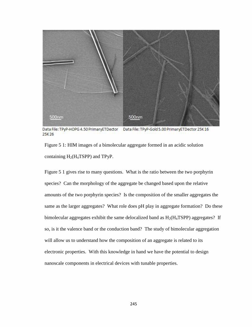
245
Figure 5 1: HIM images of a bimolecular aggregate formed in an acidic solution
containing H2(H4TSPP) and TPyP.
Figure 5 1 gives rise to many questions. What is the ratio between the two porphyrin
species? Can the morphology of the aggregate be changed based upon the relative
amounts of the two porphyrin species? Is the composition of the smaller aggregates the
same as the larger aggregates? What role does pH play in aggregate formation? Do these
bimolecular aggregates exhibit the same delocalized band as H2(H4TSPP) aggregates? If
so, is it the valence band or the conduction band? The study of bimolecular aggregation
will allow us to understand how the composition of an aggregate is related to its
electronic properties. With this knowledge in hand we have the potential to design
nanoscale components in electrical devices with tunable properties.
246
Chapter 6: Conclusions
Revisiting the stated goals of this project outlined in the introduction:
1. To measure UV-visible and RLS spectra of monomeric H2(H4TSPP) and it‟s
aggregate to verify the aggregation of H2(H4TSPP) and to parse the electronic
spectrum into monomeric and aggregate components.
We have confirmed the aggregation of H2(H4TSPP) by UV-visible and RLS. The 490
nm band is assigned to the nanorod due to the high RLS signal at 490 nm. The
assignment of the 424 and 707 nm bands is uncertain. The scattering intensities of
the 490 nm and 707 nm ban track with each other indicating that the 707 nm and 490
nm bands arise from the same species. On the other hand UV-visible experiments
link the 424 nm and 707 nm band together. More experiments are needed to
understand the scattering and UV-visible data. The 434, 595, and 644 nm peaks in
the Uv-visible spectrum are assigned to the diacid monomer.
2. To conduct AFM studies on H2(H4TSPP) nanotubes deposited on substrates to
characterize the dimensions of the tubes.
AFM analysis indicates that H2(H4TSPP) nanotubes can be deposited on Au(111) and
HOPG. The nanotubes have consistent heights and widths from substrate to
substrate (30 nm and 4 nm respectively) and vary greatly in length from a few
hundred nm to over a micron.
3. To conduct STM studies on both monomeric H2(H4TSPP) and it‟s aggregate in order
to test the validity of the proposed aggregation models.
247
STM analysis of H2(H4TSPP) nanotubes on Au(111) and HOPG is consistent with
the dimensions from AFM. The only substructure visible by ambient STM was disk-
like which is likely the result of a side reaction with gold.
4. To carry out Raman studies of the H2(H4TSPP) monomer and nanotubes in solution
to investigate the effects of aggregation on the vibrational structure of the system.
We will also report Raman spectra of nanotubes deposited on Au(111) and compare
with solution data.
Raman spectra of the H2(H4TSPP) monomer and nanotubes show small shifts in
vibrational frequencies upon aggregation along with large increases in the intensity
of the low frequency modes. Comparison of solution spectra and spectra of the
aggregates deposited on Au(111) demonstrates intact deposition of the tubes on
Au(111).
5. To conduct compositional testing on the deposited monomer and aggregate by XPS.
XPS tests of the TSPP powders indicate that the chloride salt is the better starting
material. XPS data of deposited nanorods on Au(111), HOPG, and the monomer on
HOPG show that there is no compositional change upon aggregation and/or
deposition.
6. To conduct the first reported STM I(V) study of both the monomer and aggregate to
investigate the effects of aggregation on the electronic structure of the system. Save
Otsuka et al. the I(V) studies covered in the review were all constrained to bias
voltages less than one volt. We will report on the I(V) characteristics of monomeric
H2(H4TSPP) and it‟s aggregate over a range of ±2 V.
248
UHV-STM confirmed the presence of two different surface structures of monomeric
H2(H4TSPP) on HOPG. H2(H4TSPP) nanotubes were visualized on Au(111) and
HOPG. I(V) measurements confirmed the presence of a LUMO at 1.3 V in
monomeric H2(H4TSPP) which, upon aggregation, couples to form a highly
conducting valence band in the aggregate extending from 1.3 V to at least 2 V. No
delocalized valence band was seen in the aggregate down to -2 V.
7. To deposit the nanotubes on an interdigitated electrode and measure the conductivity
of the aggregates across the long axis of the tubes over a range of ±2 V.
Some I(V) measurements were carried out which supported the STM I(V) data. The
device suffered from design issues and high capacitance.
8. To conduct the first reported HIM studies on H2(H4TSPP) nanotubes in order to test
the validity of the proposed aggregation models.
HIM images were consistent with the widths observed by STM and AFM. The
nanorods did not scatter well and appeared dark in the HIM images. The
microscope’s resolution was insufficient to resolve aggregate substructure.
9. To conduct TEM studies on H2(H4TSPP) nanotubes in order to test the validity of the
proposed aggregation models.
TEM images were consistent with the widths observed by STM and AFM. The
nanorods suffered from poor contrast in the TEM images. The microscope’s
resolution was insufficient to resolve aggregate substructure.
249
References
1 Treibs, A. E.; Angewandte Chemie 1936, 49, 682.
2 Stone, A.; Fleisher, E. B. JACS 1968, 90, 2735-2748.
3 Hu, J. S.; Ji, H. X.; Wan, L. J. J. Phys. Chem. C 2009, 113, 16259-16265.
4 Gouterman, M. J. Chem. Phys. 1959, 30, 1139.
5 Campbell, W. M.; Jolley, K. W.; Wagner, P.; Wagner, K.; Walsh, P. J.; Gordon, K. C.;
Schmidt-Mende, L.; Nazeerudding, M. K.; Wang, Q.; Gratzel, M.; Officer, D. L. J. Phys.
Chem. C Lett. 2007, 111, 11760-11762.
6 Yao, C.; Yan, L.; Guan, L.; Liu, C.; Song, P.; Su, Z. Dalton Trans, 2010, 39, 7645-
7649.
7 Thyagariajan, S.; Leiding, T.; Arskold, S. P.; Cheprakov, A. V.; Vinogradov, S. A.
Inorganic Chemistry, 2010, DOI: 10.1021/ic100968p.
8 Riberio, S. M.; Serra, A. C.; Rocha Gonsalves, A. M. d‟A. Journal of Molecular
Catalysis A 2010, 326, 121-127.
9 Verma, A.; Facchina, S. L.; Hirsch, D. J.; Song, S.; Dillahey, L. F.; Williams, J. R.;
Synder, S. H. Molecular Medicine 1998, 4, 40-45.
10Fuhrhop, J. H.; Mauzerall, D. J.A.C.S. 1969, 91, 4174-4181.
11 Pekkarinen, L.; Linschitz, H. J.A.C.S. 1960, 82, 2407-2411.
12 McRae, E. G. Aust. J. Chem. 1961, 14, 329-348.
13 Kasha, M.; McRae, E. G. Radiation Research, 1963, 20, 55.
14 Whitesides, G. M.; Mathias, J .P.; Seto, C. T. Science, 1991, 254, 1312-1319.
15 Hu, X.; Schulten, K. Physics Today August 1997, 28-34.
250
16
Zhou, Q.; Li, C. M.; Li, J.; Lu, J. J. Phys. Chem. C 2008, 112, 18578-18583.
17 Rao, C. N. R.; Agrawal, V. V.; Biswas, K.; Gautam, U. K.; Ghosh, M.; Govindaraj, A.;
Kulkarni, G. U.; Kalyanikutty, K. P.; Sardar, K.; Vivekchand, S. R. C. Pure and Applied
Chemistry 2006, 78, 1619-1650.
18 Wang, Y.; Zhou, W.. J. Nanosci. Nanotech. 2010, 10, 1563-1583.
19 Brock, S. L. Angewan. Chemie, Int. Ed. 2009, 48, 7484-7486.
20 Tenne, R. Chemistry of Nanostructured Materials 2003, 147-182.
21 Seayad, A. M.; Antonelli, D. M. Advanced Materials (Germany) 2004, 16, 765-777.
22 Haruta, M. Catal. Today 1997, 36, 153-156.
23 Jain, P. K.; El-Sayed, M. A. Chem. Phys. Lett. 2010, 487, 153-164.
24 Le Moal, E.; Fort, E.; Leveque-Fort, S. Actualite Chimique 2009, 332, 36-44.
25 Zhang, J. Z. J. Phys. Chem. Lett. 2010, 1, 686-695.
26 Khomutov, G. B.; Koksharov, Y. A. Advances in Colloid and Interface Science 2006,
122, 119-147.
27 Stoyanov, S. R.; Titov, A. V.; Kral, P.. Coord. Chem. Rev. 2009, 253, 2852-2871.
28 Avasthi, D. K.; Kumar, A.; Singhal, R.; Tripathi, A.; Misra, D. S. J.Nanosci. Nanotech.
2010, 10, 3767-3779.
29 Wen, Z.; Li, J. J. Mat. Chem. 2009, 19, 8707-8713.
30 Kamat, P. V. J. Phys. Chem. Lett. 2010, 1, 520-527.
31 Benard, P.; Chahine, R. Solid-State Hydrogen Storage 2008, 261-287.
32 Sepehri, S.; Cao, G. Annual Review of Nano Research 2010, 3, 487-514.
33 Yum, K.; Wang, Ning; Yu, M. F.. Nanoscale 2010, 2, 363-372.
251
34
Deriu, A.; Di Bari, M. T.; Gerelli, Yuri. Zeitschrift fuer Physikalische Chemie
2010,224, 227-242.
35 Braunschweig, A. B.; Schmucker, A. L.; Wei, D.; Mirkin, C. A. Chem. Phys. Lett.
2010, 486, 89-98.
36 Berven, C. A.; Dobrokhotov, V.; McIlroy, D. N.; Chava, S.; Abdelrahaman, R.;
Heieren, A.; Dick, J.; Barredo, W. IEEE Sensors Journal 2008, 9, 930-935.
37 Avasthi, D. K.; Kumar, A.; Singhal, R.; Tripathi, A.; Misra, D. S. J. Nanosci.
Nanotech. 2010, 10, 3767-3779.
38Torres -Costa, V.; Martin-Palma, R. J. J. Materials Sci. 2010, 45, 2823-2838.
39 Moshfegh, A. Z. J. Phys. D 2009, 42, 233001/1-233001/30.
40 Banhart, F. Nanoscale 2009, 1, 201-213.
41 Zhang, X.; Wang, Q.; Wu, L,; Lv, W.; Lu, J.; Bian, Y.; Jiang, J. J. Phys. Chem. B
2010, 114, 1233-1240.
42 Djurisic, A. B.; Ng, A. M. C.; Cheung, K. Y.; Fung, M. K.; Chan, W. K. J. Mater. Sci.
& Technol. (Shenyang, China) 2008, 24, 563-568.
43 Karl, N. Proceedings International School of Physics “Enrico Fermi” 2002, 149
th
(Organic Nanostrucutres: Science and Applications), 25
44 Shi N. E; Yin, G.; Han, M.; Jiang, L.; Xu, Z,; Chem. Eur. J. 2008, 14, 6255-9.
45 Kamat, P. V. J. A. C. S. 2008, 130, 14020-143019.
46 Krueger, A. Nachrichten aus der Chemie 2009, 57, 273-279.
47 Xi, H.; Wei, Z.; Duan, Z. Xu, W.; Zhu, D. J. Phys. Chem. C 2008, 112, 19934-38.
252
48
Hasobe, T.; Oki, H.; Sandanayaka, A. S. D.; Murata, H. Chem. Commun. 2008, 724-
726.
49 Schwab, A. D.; Smith, D. E.; Bond-Watts, B.; Johnson, D. E.; Hone, J.; Johnson, A. T.;
de Pula, J. C.; Smith, W. F. Nano Lett. 2004, 4, 1261-1265.
50 Medforth, C. J.; Wang, Z.; Martin, K. E.; Song, Y.; Jacobsen, J. L.; Shelnutt, J. A.
Chem. Commun. 2009, 47, 7241-7277.
51 Schwab, A.; Smith, D. E.; Rich, C. S.; Young, E. R.; Smith, W .F.; de Paula, J. C. J.
Phys. Chem. B, 2003, 107, 11339-11345.
52 Drain, C. M.; Varotto, A.; Radivojevic, I. Chem. Rev. 2009, 109, 1630-1658.
53 Dini F.; Martinelli, E.; Pomarico, G.; Paolesse, R.; Monti, D.; Filippini, D.; D'Amico,
A.; Lundstrom, I.; Di Natale, C. Nanotechnology 2009, 20, 055502.
54 Sun, D.; Tham, F. S.; Reed, C. A.; Chaker, L.; Burgess, M.; Boyd, P. D. W. J. Am.
Chem. Soc. 2000, 122, 10704-10705.
55 Wu, J.; Fang, F.; Lu, W. Y.; Hou, J. L.; Li, C.; Wu, Z. Q.; Jiang, X. K.; Li, Z. T.; Yu,
Y. H.; J. Org. Chem. 2007, 72, 2897-2905.
56 Vinodu, M.; Goldberg, I. CrystEngComm 2005, 7, 133-138.
57 Hofkens, J.; Latterini, L.; Vanoppen, P.; Faes, H.; Jeuris, K.; De Feyter, S.; Kerimo, J.;
Barbara, P. F.; De Schryver, F. C.; Rowan, A. E.; Nolte, R. J. M. J. Phys. Chem. B 1997,
101, 10588-10598.
58 Kubat, P.; Lang, K.; Janda, P.; Anzenbacher, P. Langmuir 2005, 21, 9714-9720.
59 Choi, M. Y.; Pollard, J. A.; Webb, A.; McHale J. L. J. AM. CHEM. SOC. 2003, 125,
810-820.
253
60
Doan, S. C.; Shanmugham, S.; Aston, D. E.; McHale, J. L. J. Am. Chem. Soc. 2005,
127, 5885-5892.
61 Kubat, P.; Lang, K.; Mosinger, J.; Wagnerova, D. M. Zeitschrift fuer Physicalische
Chemie, Bd 1999, 210, 243-256.
62 Vlaming, S. M.; Augulis, R.; Stuart, M. C. A.; Knoester, J.; van Loosdrecht, P. H. M.
J. Phys. Chem. B 2009, 113, 2273-2283.
63 Micali, N.; Romeo, A.; Lauceri, R.; Purrello, R.; Mallamace, F.; Scolaro, L. M. J.
Phys. Chem. B 2000, 104, 9416-9420.
64 Akins, D. L.; Zhu, H. R.; Guo, C. J. Phys. Chem. 1996, 100, 5420-5425.
65 Maiti, N. C.; Mazumdar, S.; Periasamy, N. J. Porphyrins Phthalocyanines 1998, 2,
369-376.
66 Escudero, C.; El-Hatchemi, A.; Crusats, J.; Ribo, J. M. J. Porph. Phthal. 2005, 9, 852-
863.
67 Miura, A.; Shibata, Y.; Chosrowjan, H.; Mataga, N.; Tamai, N. Journal of
Photochemistry and Photobiology A 2006, 178, 192-200.
68 Ribo, J. M.; Crusats, J.; Jarrera, J. A.; Valero, M. L. J. Chem. Soc. Chem. Commun.
1994, 681-682.
69 Micali, N.; Mallamace, F.; Romeo, A.; Purrello, R.; Scolaro, L. M. J. Phys. Chem. B
2000, 104, 5897-5904.
70 Micali, N.; Villari, V.; Castriciano, M. A.; Romeo, A.; Scolaro, L. M J. Phys. Chem. B
2006, 110,
8289-8295.
254
71
Gandini, S. C. M.; Gelamo, E. L.; Itri, R.; Tabak, M. Biophys. J. 2003, 85, 1259-1268.
72 Ohno, O.; Kaizu, Y.; Kobayashi, H. J. Chem. Phys. 1993, 99, 4128-4139.
73 Snitka, V.; Rackaitis, M.; Rodaite, R. Sens. Actuators, B 2005, 109, 159-166.
74 De Luca, G.; Romeo, A.; Scolaro, L.M. J. Phys. Chem. B, 2006, 110, 7309-7315.
75 Simkiene, I.; Sabataityte, J.; Babonas, G. J.; Reza, A.; Beinoras, J. Materials Science
and Engineering C, 2006, 26, 1007-1011.
76 Ren, B.; Tian, Z. Q.; Guo, C.; Akins, D. L. Chemical Physics Letters, 2000, 328, 17-
22.
77 Chen, D. M.; He, T.; Cong, D. F.; Zang, Y. H.; Liu, F. C. J. Phys. Chem. A, 2001, 105,
3981-3988.
78 Castriciano, M. A.; Romeo, A.; Scolaro, L. M. Journal of Porphyrins Phthalocyanines
2002, 6, 431-438.
79 Frolov, D.; Bagdonas, S.; Kelbauskas, L.; Dietel, W.; Streckyte, G.; Rotomiskis, R.
Lithuanian Journal of Physics, 2001, 41, 484-494.
80 Akins, D.L.; Zhu, H. R.; Guo, C. J. Phys. Chem. 1994, 98, 3612-3618.
81 Aggarwal, L. P. F.; Borissevitch, I. E. Spectrochimica Acta Part A 2006, 63, 227-233.
82 Collini, E.; Ferrante, C.; Bozio, R. J. Phys. Chem. C 2007, 111, 18636-18645.
83 Kano, H.; Kobayashi, T. Bull. Chem. Soc. Jpn. 2002, 75, 1071-1074.
84 Maiti, N. C.; Ravikanth, M.; Mazumdar, S.; Periasamy, N.; J. Phys. Chem. 1995, 99,
17192-17197.
85 Maiti, N. C.; Mazumdar, S.; N. Periasamy, N. J. Porphyrins Phthalocyanines 1998, 2,
369-376.
255
86
Gandini, S. C. M.; Yushmanov, V. E.; Borissevitch, I. E.; Tabak, M. Langmuir 1999,
15, 6233-6243.
87 Wu, J. J.; Li, N.; Li, K. E.; Liu, F. J. Phys. Chem. B 2008, 112, 8134-8138.
88 Purrello, R.; Bellacchio, E.; Gurrieri, S.; Lauceri, R.; Raudino, A.; Scolaro, L. M.;
Santoro, A. M. J. Phys. Chem. B 1998, 102, 8852-8857.
89 Pasternack, R. F.; Fleming, C.; Herring, S.; Collings, P. J.; dePaula, J.; DeCastro, G.;
Gibbs, E. J. Biophysical Journal 2000, 79, 550-560.
90 Ribo, J. M.; Rubires, R.; El-Hachemi, Z.; Farrera, J. A.; Campos, L.; Pakhomov, G. L.;
Vendrell, M. Mater. Sci. Eng. C 2000, 11, 107-115.
91 Castriciano, M. A.; Romeo, A.; Villari, V.; Micali, N.; Scolaro, L. M. J. Phys. Chem. B
2003, 107, 8765-8771.
92 Gulbinas, V.; Karpicz, R.; Augulis. R.; Rotomiskis, R. Chemical Physics 2007, 332,
255-261.
93 McRae, E. G.; Kasha, M. Physical Processes in Radiation Biology; Augenstein, L.,
Mason, R., Rosenberg, B., Eds.; Academic Press: New Yourk 1964: p 23
94 Ogawa, T.; Tolumaga, E.; Kobayashi, T. Chem. Phys. Lett. 2005, 408, 186-191.
95 Zimmermann, J.; Siggel, I.U.; Fuhrhop, J.H.; Roder, B.J.M.; Srivastava, T.S.;
Chatterjee, A. J. Phys. Chem. B 2003, 107, 6019-6021.
96 Kano, H.; Saito, T.; Kobyashi, J. J. Phys. Chem. B 2001, 105, 413-419.
97 Shelnutt, J. A. J. Chem. Phys. 1981, 74, 6644-6657.
98 Pasternack, R. F.; Collings, P. J. Science 1995, 269, 935-939.
99 Pasternack, R. F.; Schaefer, K. F. Inorg. Chem. 1994, 33, 2062-2065.
256
100
Collings, P. J.; Gibbs, E. J.; Starr, T. E.; Vafek, O.; Yee, C.; Pomerance, L. A.;
Pasternack, R. A. J. Phys. Chem. B 1999, 103, 8474-8481.
101 Koti, A. S. R.; Periasamy, N. Chemistry of Materials 2003, 15, 369-371.
102 Chen, D. M.; He, T.; Cong. D. F.; Zhang, Y. H.; Liu, F. C. J. Phys. Chem. A 2001,
105, 3981-3988.
103 Kitahama, Y.; Kimura, Y.; Takazawa, K. Langmuir 2006, 22, 7600-7604.
104 Maiti, N. C.; Mazumdar, S.; Periasamy, N. J. Phys. Chem. B 1998, 102, 1528-1538.
105 Rotomiskis, R.; Augulis, R.; Snitka, V.; Valiokas, R.; Liedberg, B. J. Phys. Chem. B
2004, 108, 2833-2838.
106 Escudero, C.; Crusats, J.; Diez-Perez, I.; El-Hachemi, Z.; Ribo, J.M. Angew. Chem.
Int. Ed., 2006, 45, 8032-8035.
107 Miura, A.; Shibata, Y.; Chosrowjan, H.; Mataga, N.; Tamai, N. Journal of
Photochemistry and Photbiology A 2006, 178, 192-200.
108 Shimidzu, T.; Segawa, H.; Wu, F.; Nakayama, N. J. Photochem. Photobiol. A 1995,
92, 121-127.
109 Liu, C.; Tang, H.; Bard, A. J. J. Phys. Chem. 1996, 100, 3587-3591.
110 Fox, M. A.; Bard, A. J. Science 1993, 261, 897-899.
111 Riley, K. C.; Muller, E. A.; Feldman, B. E.; Cross, C. M.; Van Aken, K. L.; Johnston,
D. E.; Lu, Y.; Johnson, A. T.; de Paula, J. C.; Smith, W. F. J. Phys. Chem. C 2010, 114,
19227-19233.
112 Yeats, A. L.; Schwab, A. D.; Massare, B.; Johnston, D. E.; Johnson, A. T.; de Paula, J.
C.; Smith, W. F. J. Phys. Chem. C 2008, 112, 2170-2176.
257
113
Otsuka, Y.; Naitoh, Y.; Matsumoto, T.; Mizutani, W.; Tabata, H.; Kawai, T.
Nanotechnology 2004, 15, 1639-1644.
114 Rubires, R.; Muller, C.; Campos, L.; El-Hachemi, Z.; Pakhomov, G. L.; Rbo, J. M. J.
Porph. Phth, 2002, 6, 107-113.
115 Gouterman, M.; The Porphyins Vol III 1978 Academic Press Inc.
116 Gouterman, M.; J. Chem. Phys. 1959, 30, 1139-1161.
117 Linder, R. E.; Barth, G.; Bunnenberg, E.; Djerassi, C.; Seaman, L.; Moscowitz, A.
Journal of the Chemical Society, Perkin Transactions II 1974, 14, 1712-1718
118 Kasha, M.; Rawls, H. R.; Ashraf El-Bayoumi, M. Pure and Applied Chemistry, 1965,
11, 371-392.
119 Pasternack, R. F.; Bustamante, C.; Collings, P. J.; Giannetto, A.; Gibbs, E. J.; J. Am.
Chem. Soc. 1993, 115, 5393-5399.
120 Lu, W.; Band, B. S.; Yu, Y.; Li, Q. G.; Shang, J. C.; Wang, C.; Fang, Y.; Tian, R.;
Zhou, L. P.; Sun, L. L.; Tang, Y.; Jing, S. H.; Huang, W.; Zhang, J. P.; Microchim Acta
2007, 158, 29-58.
121 Stanton, S. G.; Pecora, R. J. Chem. Phys. 1981, 75, 5615-5626.
122 Einstein, A. Ann. Physik 1905, 17, 132-148.
123 Brundle, C. R. J. Vac. Sci. Technol. 1974, 11, 212-224.
124 Briggs, D. Handbook of X-ray and Ultraviolet Photoelectron Spectroscopy 1977
Heyden & Son Ltd.
125 Alov, N.V. Journal of Analytical Chemistry 2005, 60, 297-300
126 Swartz, W. Analytical Chemistry 1973, 45, 788-795.

258
127
Hamers, R. J. Annu. Rev. Phys. Chem. 1989, 40, 531-559.
128 Hipps; K.W. in “Handbook of Applied Solid State Spectroscopy”, Ed: Vij, D.R.,
Springer Verlag (2006) ISBN: 0-387-32497-6
129 Wiebe, J.; Wachowiak, A.; Meier, F.; Haude, D.; Foster, T.; Morgenstern, M.;
Wiesendager, R. Review of Scientific Instrumentation 2004, 75, 4871-4879.
130 Kowalczyk, P. Applied Surface Science 2007, 253, 4036-4040.
131 Giessibl, F. J. Rev. Mod. Phys., 2003, 75, 949-983.
132 Moskovits, M. J. Chem. Phys. 1982, 77, 4408-4416.
133 Dowdy, J.; Hoagland, J. J.; Hipps, K. W. J. Phys. Chem. 1991, 95, 3751-5755.
134 Morgan, J.; Notte, J.; Hill, J.; Ward, B. Microscopy Today, 2006, 14, 24-31.
135 Scipioni, L.; Sanford, C. A.; Notte, J.; Thompson, B.; McVey, S. J. Vac. Sci. Technol.
B 2009, 27, 3250-3255.
136 Carl Zeiss website http://www.smt.zeiss.com/c1256e4600305472/Contents-
Frame/e87f4889b0612d9bc125734f00373b5f Accessed 12/6/10
137 Hitachi website http://www.hhtc.ca/microscopes/sem/s5500.htm accessed 12/6/10
138 Scipioni, L.; Stern, L. A.; Notte, J.; S. Sijbrandij, Griffin, B. Advanced Materials &
Processes 2008, 27-30.
139 Misell, D. L. J. Phys. D: Appl. Phys., 1977, 10, 1085-1107.
140 Reimer, L.; Transmission Electron Microscopy 4
th ed Springer-Verlag (1997) ISBN:
3-540-56849-2
141 FEI website http://www.fei.com/products/transmission-electron-
microscopes/titan.aspx accessed 12/6/10
259
142
Sobotik, P.; Ostadal, I. Journal of Crystal Growth, 1999, 197, 955-962
143 Mahmudur, R.; Harmon, J.H.; J. Porph. Phth. 2007, 11, 125-129.
144 Ribo, J. M.; Crusats, J.; Farrera, J. A.; Valero, M. L. J. Chem. Soc., Chem. Commun.
1994, 681-682.
145 Castriciano, M. A.; Romeao, A.; Villari, V.; Micali, N.; Scolaro, L. M. J. Phys. Chem.
B 2003, 107, 8765-8771.
146 Rubires, R.; Cursats, J.; El-Hatchemi. Z.; Jaramillo, T.; Lomez, M.; Valls. E.; Farrera,
J.A.; Ribo, J. New J. Chem. 1999, 189-198.
147 Andrade, S. M.; Costa, S. M. B. Chem. Eur. J. 2006, 12, 1046-1057.
148 Huang, C. Z.; Li, Y. F.; Li, N.; Li, K. A.; Tong, S.Y. Bull. Chem. Soc. Jpn. 1998, 71,
1791-1797.
149 Guo, C.; Ren, B.; Akins, D. L. J. Phys. Chem. B 1998, 102, 8751-8756.
150 Delmarre, D.; Meallet-Renault, R.; Bied-Charreton, C.; Pasternack, R. F. Analytica
Chimica Acta 1999, 401, 125-128.
151 Crusats, J.; Claret, J; Diez-Perez, I.; El-Hachemi, Z.; Garcia-Ortega, H.; Rubires, R.;
Sagues, F.; Ribo, J. M. Chem. Commun. 2003, 13, 1588-1589.
152 Egawa, Y.; Hayashida, R.; Anzai, J.I. Langmuir 2007, 23, 13146-13150.
153 de Paula, J. C.; Robblee, J. H.; Pasternack, R. F.; Biophysical Journal 1995, 68, 335-
341
154 Chan, I. Y.; Hallock, A. J. J. Chem. Phys. 1997, 107, 9297-9301.
155 Clemmer, C. R.; Beebe, T. P. Science 1991, 251, 640-642.
156 Pong, W.-T.; Bendall, J.; Durkan, C. Surf. Sci. 2007, 601, 498-509.
260
157
Augulis, R.; Tamuliene, J.; Tamulis, A.; Rotomiskis, R. Diffus. Defect. Data, SSP
2004, 97, 225-228.
158 McDermott, G.; Prince, S. M.; Freer, A. A.; Hawthornthwalte-Lawless, A. M.; Papiz,
M. Z.; Cogdell, R. J.; Isaacs, N. W. Nature 1995, 374, 517-521.
159 Ranck, J. -L.: Ruiz, T.; Pehau-Arnaudet, G.; Arnoux, B.; Reiss-Husson, F. Biochim.
Biophys. Acta 2001, 1506, 67-78.
160 Hamor, J. J.; Hamor, T. A.; Hoard, J. L. J. Am. Chem. Soc. 1964, 86, 1938-1942.
161 Rosa, A.; Ricciardi, G.; Baerends, E. J.; Romeo, A.; Scolaro, L. M. J. Phys. Chem. A
2003, 107, 11468-11482.
162 Mazur, U.; Hipps, K. W. J. Phys. Chem. 1999, 103, 9721-9727.
163 Hansen, W. N.; Hansen, G. Surf. Sci. 2001, 481, 172-184.
164 Hori, T.; Aratani, N.; Takagi, A.; Matsumoto, T.; Kawai, T.; Yoon, M. C.; Yoon, Z.
S.; Cho, S.; Kim, D.; Osuka, A. Chem. Eur. J. 2006, 12, 1319-1327.
165 Dempster, S. E.; Jang, S.; Silbey, R. J. J. Chem. Phys. 2001, 114, 10015-10023.
166 Shelnutt, J. A. J. Chem. Phys. 1981, 74, 6644-6657.
167 Shimidzu, T.; Iyoda, T.; Segawa, H.; Honda, K. New Journal of Chemistry 1986, 10,
213
168 Habib, A.; Tabata, M.; Wu. Y.G. J Porph. Phth. 2004, 8, 1269-1275
169 Li, X. Y.; Czernuszewicz, R. S.; Kincaid, J. R.; Spiro, T. G. J. Am. Chem. Soc. 1989,
111, 7012-7023.
170 Bell, S. E. J.; Al-Obadi, A. H. R.; Heagarty, M.; McGarvey, J. J. J. Phys. Chem. 1995,
99, 3959-3964.
261
171
Saini, G. S. S. Spectrochimica Acta Part A, 2006, 64, 981-986.
172 Bell, S. E. J.; Al-Obadi, A. H. R.; Heagarty, M.; Hester, R. E.; McGarvey, J. J. J.
Phys. Chem. 1993, 97, 11599-11602.
173 Rosa, A.; Ricciardi, G.; Baerends, E. J.; Romeo, A.; Scolaro, L. M. J. Phys. Chem. A
2003, 107, 11468-11482.
174 Lemke, C.; Dreybolt, W.; Shelnutt, J. A.; Quirke, J. M. E.; Scweitzer-Stenner, R. J.
Raman Spectrosc. 1998, 29, 945-953.
175 Oakes, R. E.; Spence, S. J.; Bell, S. E. J. J Phys Chem. A 2003, 107, 2964-2973.
176 Dempster, S. E.; Jang, S.; Silbey, R. J. J. Chem. Phys. 2001, 114, 10015-10023.
177 Gnana, K. G.; Pil, K.; Ae Rhan, K.; Kee Suk, N.; Nimma, E.R. Materials Chemistry
and Physics 2009, 115, 40-46.
178 Moulder, J.; et. al. Handbook of X-ray Photoelectron Spectroscopy 1992 Perkin Elmer
Corporation p61
179 Yamashige, H.; Shuij, M.; Tsutomu, K.; Perera, R. C.; Hisanobu, W. Analytical
Science 2005, 21, 635-639.
180 Stypula, B.; Stoch, J. Corrosion Science, 1994, 36, 2159-2167
181 Watanabe, M.; Ando, H.; Handa, T.; Ichino, T.; Kuwaki, N. Zairyo-to-Kankyo 2007,
56, 10-15.
182 Sumi, H. J. Phys. Chem. B 1998, 102, 1833-1844.
183 Hipps, K. W.; Scudiero, L. J. Chem. Ed. 2005, 82, 704-711.
184 Yuan, O.; Xing, Y.; Borguet, E. J. A. C. S 2010, 132, 5054-5060.
185 Yoshimoto, S.; Sawaguchi, T. J. Amer. Chem. Soc. 2008, 130, 15944-15949.
262
186
Yoshimoto, S.; Sawaguchi, T. ECS Transactions 2009, 16, 77-82.
187 Yoshimoto, S.; Yokoo, N.; Fukuda, T.; Kobayashi, N.; Itaya, K.. Chem. Comm. 2006,
500-502.
188 Yokoyama, T.; Kamikado, T.; Yokoyama, S.; Mashiko, S. J. Chem. Phys. 2004, 121,
11993.
189 Nicholls, D.; McKinzie, W. P.; Oncel, N. J. Phys. Chem. C 2010, 114, 14983-14985.
190 Lei, S. B.; Wang, C.; Yin, S. X.; Wang, H. N.; Xi, F.; Liu, H.W.; Xu, B.; Wan, L.J.;
Bai, C. L. J. Phys. Chem. B 2001, 105, 10838-10841.
191 Ruoff, R. S.; Kadish, K. M.; Boulas, P.; Chen, E. C. M. J. Phys. Chem. 1995, 99,
8843-50.
192 Seki, K. Mol. Cryst. Liq. Cryst. 1989, 171, 255-270.
193 Nakato, Y.; Abe, K.; Tsubomura, H. Chem. Phys. Lett. 1976, 39, 358-361.
194 Davis, D. G. “The Porphyrins” Ed: Dolphin, D.; Chapter 4, 1978, 143-144.
195 Piet, D. P.; Danovich, D.; Zuilhof, H.; Sudholter, E. J. R. J. Chem. Soc., Perkin
Trans. 2, 1999, 1653–1661.
196 Gruhn, N. E.; Lichtenberger, L.; Ogura, H.; Walker, F. A. Inorg. Chem. 1999, 38,
4023-4027.
197 Lukasczyk, T.; Flechtner, K.; Merte, L. R.; Jux, N.; Maier, F.; Gottfried, J. M.;
Steinruck, H-P. J. Phys. Chem. C 2007, 111, 3090-3098
198 Lukasczyk, T.; Flechtner, K.; Merte, L. R.; Jux, N.; Maier, F.; Gottfried, J. M.;
Steinruck, H-P. J. Phys. Chem. C 2007, 111, 3090-3098
199 Kruk, M. M.; Braslavsky, S. E. J. Phys. Chem. A 2006, 110, 3414-3425.
263
200
Kobayashia, Y.; Kusakabe, Koichi; Fukui, Ken-ichi; Enoki, T. Physica E 2006, 34,
678-681.
201 Nicholls, D.; McKinzie, W. P.; Oncel, N. J. Phys. Chem. C 2010, 114, 14983-14985.
202 Giunta, P.L.; Kelty, S. P. Chem. Phys. 2001, 114, 1807-1812.
203 Bredie, J.; Linares, M.; Lensen, R.; Rowan, A. E.; Funk, M.; Broring, M.; Hoffmann,
G.; Wiesendanger, R. J. Vac. Sci. Technol. B 2009, 27, 799-804.
204 Segal, D.; Nitzan, A.; Davis, W. B.; Wasielewski, M. R.; Ratner, M. A. J. Phys.
Chem. B 2000, 104, 3817-3829.
205 Holmlin, R. E.; Haag, R.; Dhabinyc, M. L.; Ismagilov, R.; Cohen, A.; Terfort, A.;
Rampi, M.; Whietsides, G. M. J. Am Chem. Soc. 2001, 123, 5075-5085.
206 Sedghi G.; Sawada, K.; Esdaile, L. J.; Hoffmann, M.; Anderson, H. L.; Bethell, D.;
Haiss, W.; Higgins, S. J.; Nichols, R. J. J. AM. CHEM. SOC. 2008, 130, 8582-8583.
207 Wold, D. J.; Haag, R.; Rampi, M. A.; Frisbie, C. D.; J. Phys. Chem. B 2002, 106,
2813-2816.
208 Hirota, S.; Itoh, U.; Takada, K. Thin Solid Films 1988, 165, 337-345.
209 Scudiero, L.; Barlow, D. E.; Mazur, U.; Hipps, K. W. J. Am. Chem. Soc. 2001, 123,
4073-4080.