Embed Size (px)
Citation preview
An Energy-efficient Matrix Multiplication Accelerator
by Distributed In-memory Computing
on Binary RRAM Crossbar
Leibin Ni1, Yuhao Wang1, Hao Yu1, Wei Yang2, Chuliang Weng2, Junfeng Zhao2
1School of EEE, Nanyang Technological University, Singapore2Shannon Laboratory, Huawei Technologies Co., Ltd, China
1

Data Analytics Challenge
2
Data center for future big-data-
oriented society:
1. Leaving data outside a nation will
face serious cyber-security
concern
2. Processing data inside a nation by
traditional Giga-scale system has
high cost
Bandwidth at 100 Gps with
Space of 20,000 sq. ft. Power
of 68 MW and cost of 100M-
USD !!!
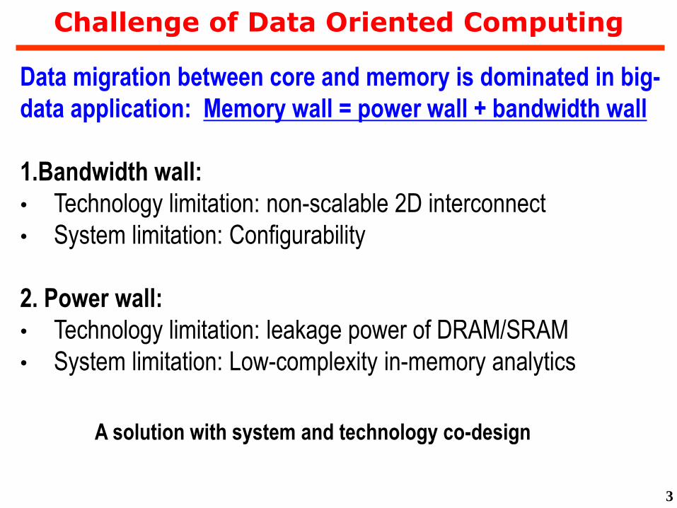
Challenge of Data Oriented Computing
Data migration between core and memory is dominated in big-
data application: Memory wall = power wall + bandwidth wall
1.Bandwidth wall:
• Technology limitation: non-scalable 2D interconnect
• System limitation: Configurability
2. Power wall:
• Technology limitation: leakage power of DRAM/SRAM
• System limitation: Low-complexity in-memory analytics
3
A solution with system and technology co-design
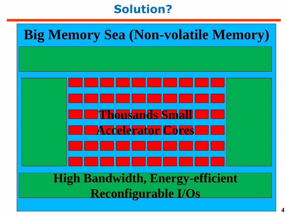
Solution?
Big Memory Sea (Non-volatile Memory)
Thousands Small
Accelerator Cores
High Bandwidth, Energy-efficient
Reconfigurable I/Os
4
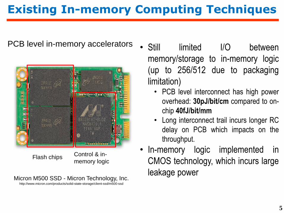
Existing In-memory Computing Techniques
Flash chipsControl & in-
memory logic
PCB level in-memory accelerators
Micron M500 SSD - Micron Technology, Inc.http://www.micron.com/products/solid-state-storage/client-ssd/m500-ssd
• Still limited I/O between
memory/storage to in-memory logic
(up to 256/512 due to packaging
limitation)• PCB level interconnect has high power
overhead: 30pJ/bit/cm compared to on-
chip 40fJ/bit/mm
• Long interconnect trail incurs longer RC
delay on PCB which impacts on the
throughput.
• In-memory logic implemented in
CMOS technology, which incurs large
leakage power
5
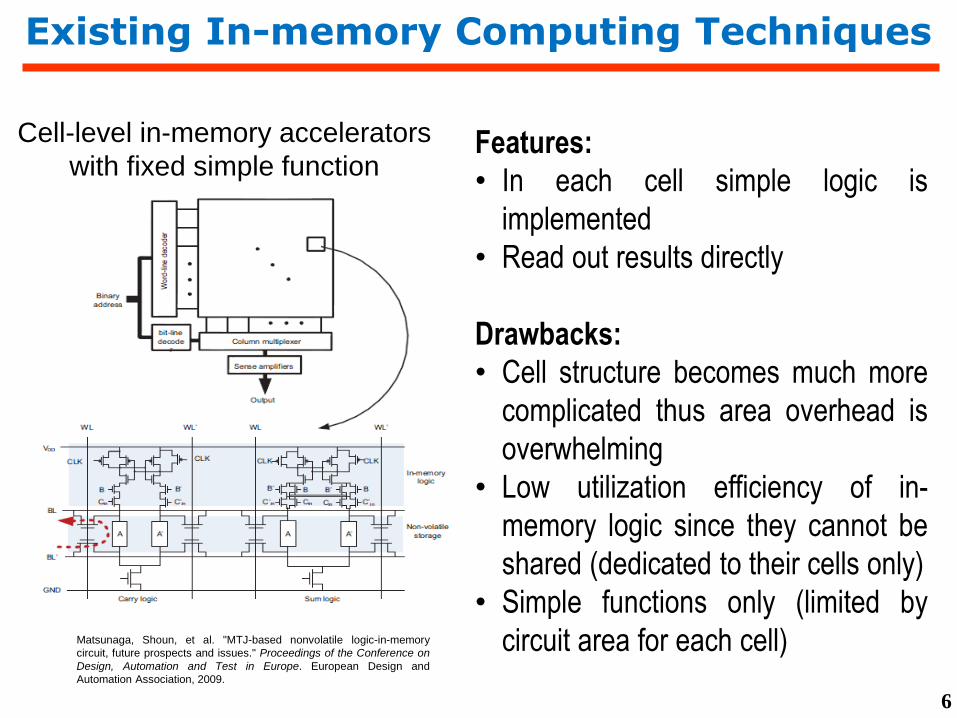
Existing In-memory Computing Techniques
Cell-level in-memory accelerators
with fixed simple function
Matsunaga, Shoun, et al. "MTJ-based nonvolatile logic-in-memory
circuit, future prospects and issues." Proceedings of the Conference on
Design, Automation and Test in Europe. European Design and
Automation Association, 2009.
Features:
• In each cell simple logic is
implemented
• Read out results directly
Drawbacks:
• Cell structure becomes much more
complicated thus area overhead is
overwhelming
• Low utilization efficiency of in-
memory logic since they cannot be
shared (dedicated to their cells only)
• Simple functions only (limited by
circuit area for each cell)
6
Non-volatile In-Memory Accelerator
7
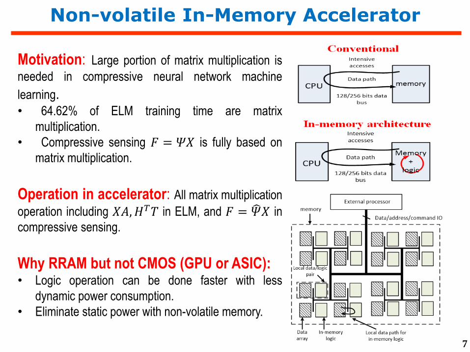
Motivation: Large portion of matrix multiplication is
needed in compressive neural network machine
learning.• 64.62% of ELM training time are matrix
multiplication.
• Compressive sensing 𝐹 = 𝛹𝑋 is fully based on
matrix multiplication.
Operation in accelerator: All matrix multiplication
operation including 𝑋𝐴,𝐻𝑇𝑇 in ELM, and 𝐹 = 𝛹𝑋 in
compressive sensing.
Why RRAM but not CMOS (GPU or ASIC):• Logic operation can be done faster with less
dynamic power consumption.
• Eliminate static power with non-volatile memory.
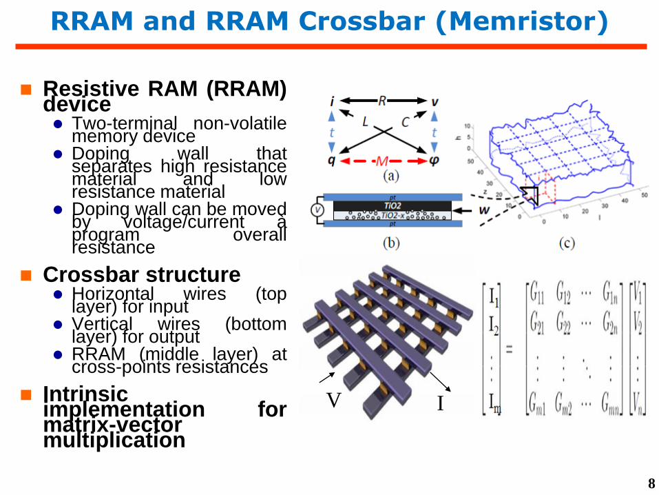
RRAM and RRAM Crossbar (Memristor)
Resistive RAM (RRAM)device Two-terminal non-volatile
memory device Doping wall that
separates high resistancematerial and lowresistance material
Doping wall can be movedby voltage/current àprogram overallresistance
Crossbar structure Horizontal wires (top
layer) for input Vertical wires (bottom
layer) for output RRAM (middle layer) at
cross-points resistances
Intrinsicimplementation formatrix-vectormultiplication
8
V I
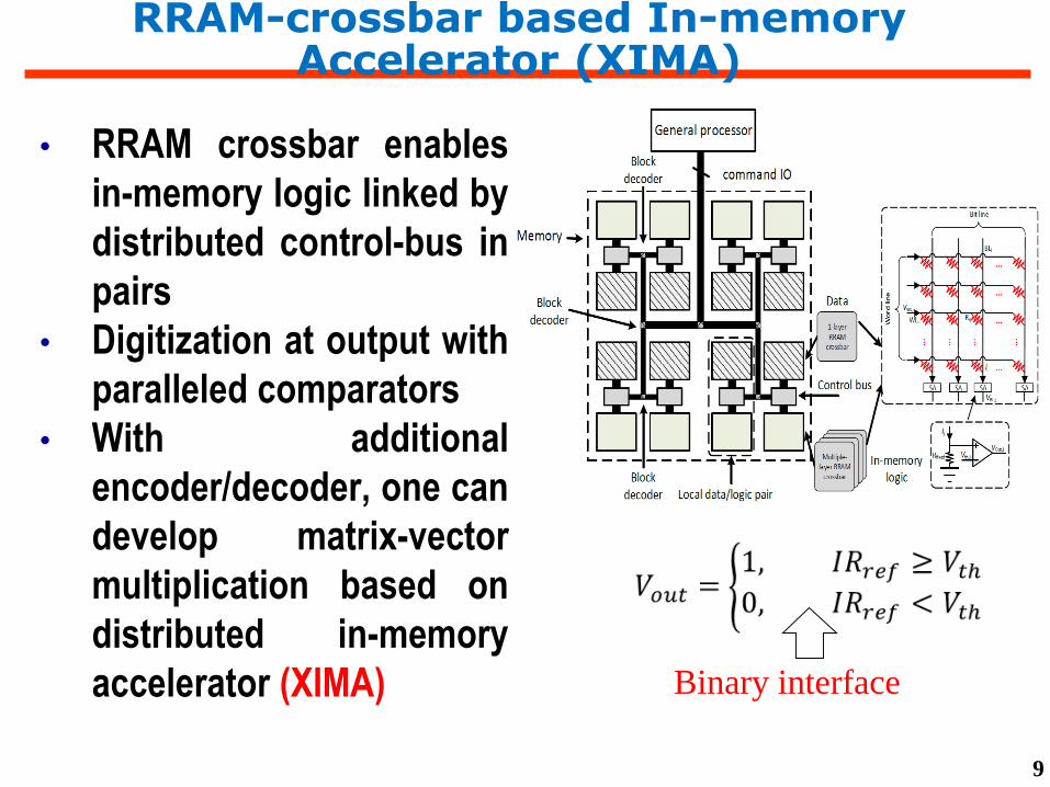
RRAM-crossbar based In-memory Accelerator (XIMA)
• RRAM crossbar enables
in-memory logic linked by
distributed control-bus in
pairs
• Digitization at output with
paralleled comparators
• With additional
encoder/decoder, one can
develop matrix-vector
multiplication based on
distributed in-memory
accelerator (XIMA) Binary interface
9
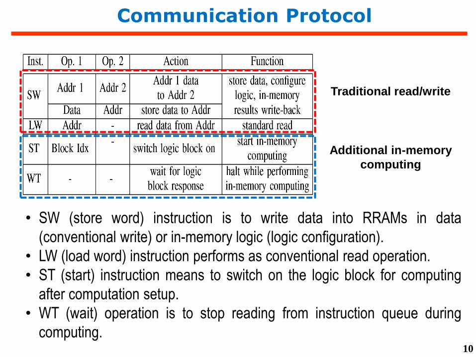
Communication Protocol
• SW (store word) instruction is to write data into RRAMs in data
(conventional write) or in-memory logic (logic configuration).
• LW (load word) instruction performs as conventional read operation.
• ST (start) instruction means to switch on the logic block for computing
after computation setup.
• WT (wait) operation is to stop reading from instruction queue during
computing.
Traditional read/write
Additional in-memory
computing
10
Control-bus Design
external processor
LogicData
1
2
3
Address decoder
In-pair CMOS control bus
Instruction queue
Instruction decoder
Data path to data array
Data path to in-memory logic
Row/Column to data array Row/Column to
in-memory logic
SRAM array
Module Block decoder
Data array 0 0…0
In-memory logic 1 Layer indexBlock index
Address decoder
In-layer address
Original data in this pair
4
Original data
2. In data array
01010001
10110011 ...
By multiple-layer RRAM crossbar logic
Processed data
3. In data array
external processor
4. Result read out
NPN
P
MM
MM
1
111
• Instruction queue: store
instructions issued by external
processor.
• Instruction decoder: analyze
instructions on a first-come-first-
serve (FCFS) basis.
• Address decoder: obtain the row
and column index from the
instruction.
• SRAM array: store temporary
data such as computation results,
which are later written back to
data array. 11
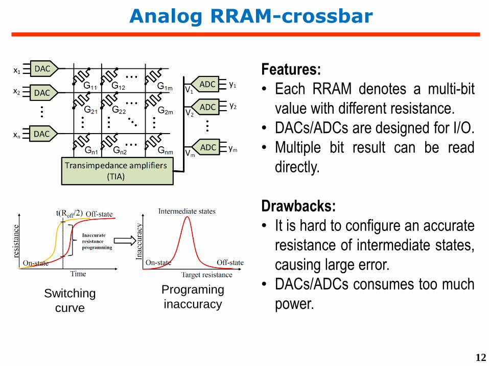
Analog RRAM-crossbar
Features:
• Each RRAM denotes a multi-bit
value with different resistance.
• DACs/ADCs are designed for I/O.
• Multiple bit result can be read
directly.
Drawbacks:
• It is hard to configure an accurate
resistance of intermediate states,
causing large error.
• DACs/ADCs consumes too much
power.Switching
curve
Programing
inaccuracy
12
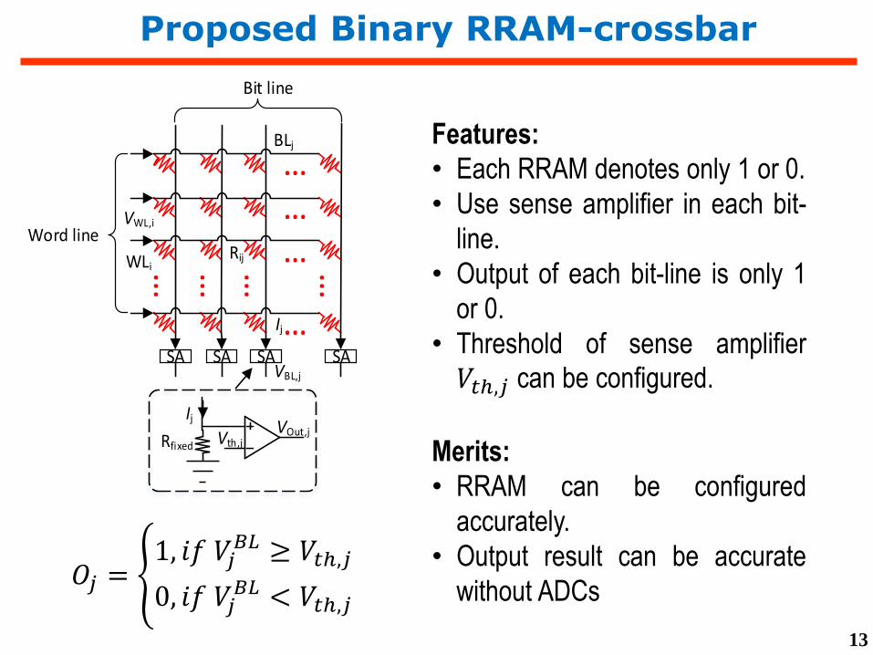
Proposed Binary RRAM-crossbar
Features:
• Each RRAM denotes only 1 or 0.
• Use sense amplifier in each bit-
line.
• Output of each bit-line is only 1
or 0.
• Threshold of sense amplifier
𝑉𝑡ℎ,𝑗 can be configured.
Merits:
• RRAM can be configured
accurately.
• Output result can be accurate
without ADCs
Word line
Bit line
WLi
BLj
Rij
Ij
VWL,i
SA SA SA SAVBL,j
Ij
Vth,jVOut,j
Rfixed
𝑂𝑗 = 1, 𝑖𝑓 𝑉𝑗
𝐵𝐿 ≥ 𝑉𝑡ℎ,𝑗
0, 𝑖𝑓 𝑉𝑗𝐵𝐿 < 𝑉𝑡ℎ,𝑗
13
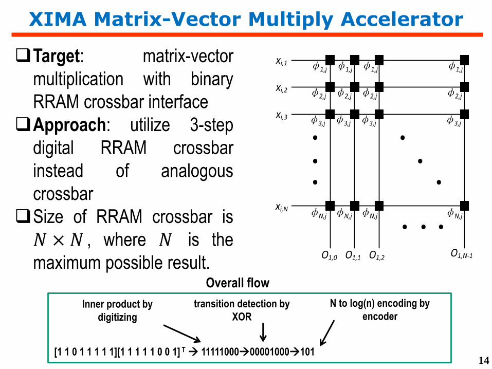
XIMA Matrix-Vector Multiply Accelerator
Target: matrix-vector
multiplication with binary
RRAM crossbar interface
Approach: utilize 3-step
digital RRAM crossbar
instead of analogous
crossbar
Size of RRAM crossbar is
𝑁 × 𝑁 , where 𝑁 is the
maximum possible result.
xi,1
xi,2
xi,3
xi,N
φ1,j
φ2,j
φ3,j
φN,j
φ1,j
φ2,j
φ3,j
φN,j
φ1,j
φ2,j
φ3,j
φN,j
φ1,j
φ2,j
φ3,j
φN,j
O1,0 O1,1 O1,2 O1,N-1
Overall flow
[1 1 0 1 1 1 1 1][1 1 1 1 1 0 0 1] T 1111100000001000101
Inner product by
digitizing
transition detection by
XOR
N to log(n) encoding by
encoder
14
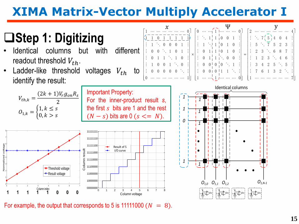
XIMA Matrix-Vector Multiply Accelerator I
Step 1: Digitizing• Identical columns but with different
readout threshold 𝑉𝑡ℎ.
• Ladder-like threshold voltages 𝑉𝑡ℎ to
identify the result:
𝑉𝑡ℎ,𝑘 =2𝑘 + 1 𝑉𝑟𝑔𝑜𝑛𝑅𝑠
2
𝑂1,𝑘 = 1, 𝑘 ≤ 𝑠0, 𝑘 > 𝑠
1
1
0
1
1
1
1
1
O1,0 O1,1 O1,2 O1,N-1
Identical columns
71
23167
55243
64321
78632
32575
40457
42
011
11000
10000
00110
010110
01011
10011
010
10
00000
01001
01110
10100
10001
11111011
01
𝑥 Ψ y
1 1 1 1 1 0 0 0
0 1 2 3 4 5 6 70
1
2
3
4
5
6
7
8
Column index
Norm
alized v
oltage
Threshold voltage
Result voltage
For example, the output that corresponds to 5 is 11111000 (𝑁 = 8).
Important Property:
For the inner-product result s,
the first 𝑠 bits are 1 and the rest
(𝑁 − 𝑠) bits are 0 (𝑠 <= 𝑁).
0 1 2 3 4 5 6 7 800000000
10000000
11000000
11100000
11110000
11111000
11111100
11111110
11111111
Column voltage
Co
lum
n r
esu
lt
Result of 5I/O curve
15
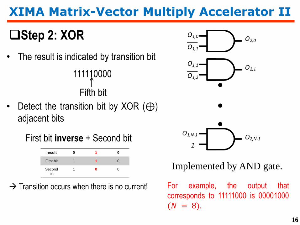
• The result is indicated by transition bit
XIMA Matrix-Vector Multiply Accelerator II
111110000
Fifth bit
Step 2: XOR
result 0 1 0
First bit 1 1 0
Second
bit
1 0 0
Transition occurs when there is no current! For example, the output that
corresponds to 11111000 is 00001000
(𝑁 = 8).
• Detect the transition bit by XOR (⊕)
adjacent bits
First bit inverse + Second bit
16
O1,0
O1,1
O1,1
O1,2
O2,0
O2,1
O1,N-1
1O2,N-1
Implemented by AND gate.
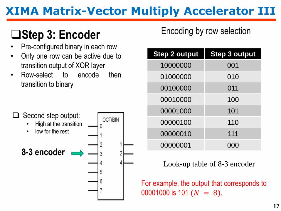
Step 3: Encoder• Pre-configured binary in each row
• Only one row can be active due to
transition output of XOR layer
• Row-select to encode then
transition to binary
XIMA Matrix-Vector Multiply Accelerator III
Encoding by row selection
Second step output:• High at the transition
• low for the rest
8-3 encoder
For example, the output that corresponds to
00001000 is 101 (𝑁 = 8).
17
Step 2 output Step 3 output
10000000 001
01000000 010
00100000 011
00010000 100
00001000 101
00000100 110
00000010 111
00000001 000
Look-up table of 8-3 encoder
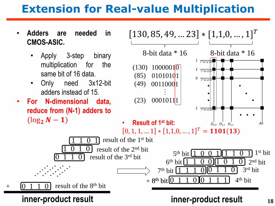
Extension for Real-value Multiplication
130, 85, 49,… 23 ∗ [1,1,0,… , 1]𝑇
8-bit data * 16 8-bit data * 16
• Adders are needed in
CMOS-ASIC.
• Apply 3-step binary
multiplication for the
same bit of 16 data.
• Only need 3x12-bit
adders instead of 15.
• For N-dimensional data,
reduce from (N-1) adders to
(log𝟐𝑵− 𝟏)
1
1
0
1
1st bit of 130
O1,0 O1,1 O1,2 Ali
1st bit of 85
1st bit of 49
1st bit of 23
10000010
01010101
00110001…00010111
(130)
(85)
(49)
(23)
• Result of 1st bit:
0, 1, 1, … 1 ∗ 1,1,0, … , 1 𝑇 = 𝟏𝟏𝟎𝟏(𝟏𝟑)
1 1 0 11 0 1 0
0 1 1 0
0 1 1 0
result of the 1st bit
result of the 2nd bit
result of the 8th bit
result of the 3rd bit
+
inner-product result
1 1 0 11 0 1 0
0 1 1 0
0 1 1 0
1st bit
2nd bit
8th bit
3rd bit
+
inner-product result
0 1 1 18th bit 4th bit
1 1 1 01 1 0 0
1 0 0 1
7th bit
6th bit
5th bit
18
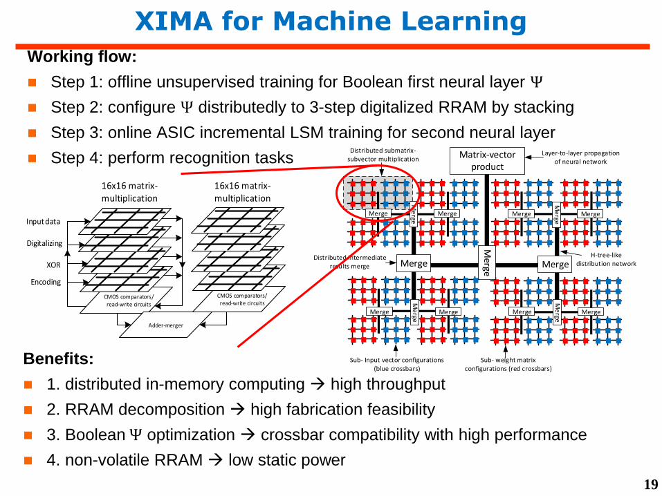
XIMA for Machine Learning
Working flow:
Step 1: offline unsupervised training for Boolean first neural layer Ψ
Step 2: configure Ψ distributedly to 3-step digitalized RRAM by stacking
Step 3: online ASIC incremental LSM training for second neural layer
Step 4: perform recognition tasks
Merge Merge
Me
rge
Merge Merge
Merge Merge
Me
rge
Merge Merge
Me
rge
Merge Merge
Me
rge
Merge
Matrix-vector product
Distributed submatrix-subvector multiplication
Distributed intermediate results merge
H-tree-like distribution network
Sub- Input vector configurations (blue crossbars)
Sub- weight matrix configurations (red crossbars)
Layer-to-layer propagation of neural network
…Benefits:
1. distributed in-memory computing high throughput
2. RRAM decomposition high fabrication feasibility
3. Boolean Ψ optimization crossbar compatibility with high performance
4. non-volatile RRAM low static power
CMOS comparators/read-write circuits
Input data
Digitalizing
XOR
Encoding
CMOS comparators/read-write circuits
Adder-merger
16x16 matrix-multiplication
16x16 matrix-multiplication
19
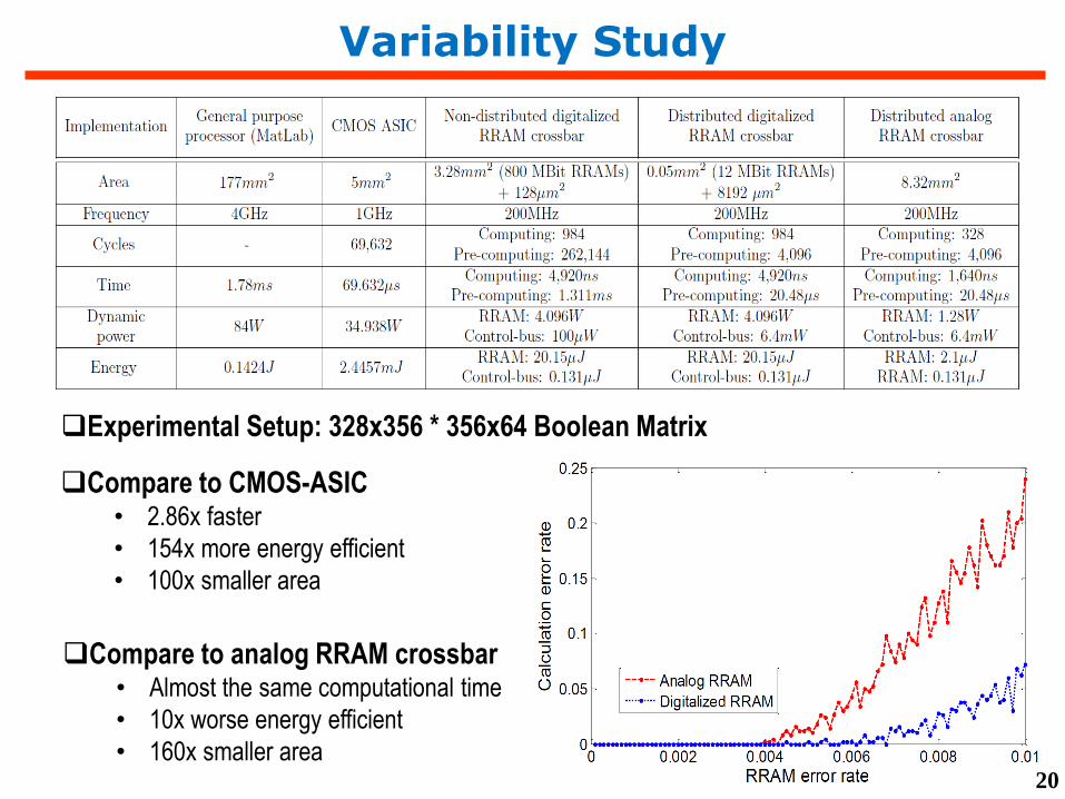
Compare to CMOS-ASIC• 2.86x faster
• 154x more energy efficient
• 100x smaller area
Compare to analog RRAM crossbar• Almost the same computational time
• 10x worse energy efficient
• 160x smaller area
Variability Study
Experimental Setup: 328x356 * 356x64 Boolean Matrix
20
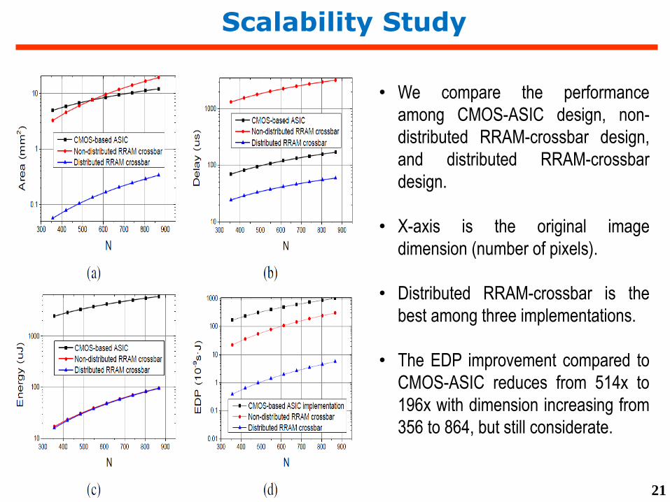
Scalability Study
• We compare the performance
among CMOS-ASIC design, non-
distributed RRAM-crossbar design,
and distributed RRAM-crossbar
design.
• X-axis is the original image
dimension (number of pixels).
• Distributed RRAM-crossbar is the
best among three implementations.
• The EDP improvement compared to
CMOS-ASIC reduces from 514x to
196x with dimension increasing from
356 to 864, but still considerate.
21
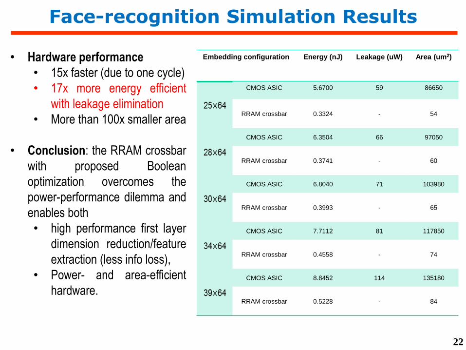
Embedding configuration Energy (nJ) Leakage (uW) Area (um2)
CMOS ASIC 5.6700 59 86650
RRAM crossbar 0.3324 - 54
CMOS ASIC 6.3504 66 97050
RRAM crossbar 0.3741 - 60
CMOS ASIC 6.8040 71 103980
RRAM crossbar 0.3993 - 65
CMOS ASIC 7.7112 81 117850
RRAM crossbar 0.4558 - 74
CMOS ASIC 8.8452 114 135180
RRAM crossbar 0.5228 - 84
• Hardware performance
• 15x faster (due to one cycle)
• 17x more energy efficient
with leakage elimination
• More than 100x smaller area
• Conclusion: the RRAM crossbar
with proposed Boolean
optimization overcomes the
power-performance dilemma and
enables both
• high performance first layer
dimension reduction/feature
extraction (less info loss),
• Power- and area-efficient
hardware.
Face-recognition Simulation Results
22