Embed Size (px)
Citation preview

8/8/2019 An Electron-cyclotron-resonance Plasma Apparatus For
http://slidepdf.com/reader/full/an-electron-cyclotron-resonance-plasma-apparatus-for 1/79
AN ELECTRON-CYCLOTRON-RESONANCE PLASMA APPARATUS FOR
HYDROG ENATED AMORPHOU S-SILICON THIN FILM PRODUCTION
by
CRAIG C. YOUNG, B.S. in M. E. , B.S. in E.E.
A THESIS
IN
ELECTRICAL ENGINEERING
Submitted to the Graduate Facultyof Texas Tech University in
Partial Fulfillment ofthe Requirements forthe Degree of
MASTER OF SCIENCE
IN
ELECTRICAL ENGINEERING
Approved
December, 1990

8/8/2019 An Electron-cyclotron-resonance Plasma Apparatus For
http://slidepdf.com/reader/full/an-electron-cyclotron-resonance-plasma-apparatus-for 2/79
73
^'^^^ ACKNOWLEDGMENTS
I would like to thank my committee members. Dr. Thomas
Trost, Dr. Magne Kristiansen, and Dr. Shubhra Gangopadhyay, for
their time and devo tion towa rds this rese arch . A special heart
felt thanks goes out to my committee chairman. Dr. Thomas Trost,
without whose guidance and perseverance I would not have been
able to attain my goals.
I would also l ike to thank everyone associated with the
Pulse d Pow er La boratory for their coop eration and dilige nce . Aspecial thanks to Kim Zinzmeyer, Chris Hatfield, Ellis Loree, and
John Bridges for the use of their ears and their endless assistance
towards the completion of this research.
To my wife Victoria, I cannot express the gratitude that she
so de se rv es . I am etern al ly inde bted to her for the
encouragement, understanding, and support she gave during this
period. Becau se you have walked beside me along my path, I will
strive to tread upon yours.
11

8/8/2019 An Electron-cyclotron-resonance Plasma Apparatus For
http://slidepdf.com/reader/full/an-electron-cyclotron-resonance-plasma-apparatus-for 3/79
CONTENTS
ACKNOWLEDGMENTS ii
ABSTRACT v
TABLES vi
nOURES vii
CHAPTER
I. INTRODUCTION 1
II. AMORPHOUS SILICON 3
Introduction 3Amorphous Silicon 6
Hydrogenated Amorphous Silicon Properties . . . . 8
The Role of Hydrogen 8
Bandgap and Carrier Transport 8Doping 11Absorpt ion 12
Hydrogenated Amorphous Silicon SolarCell Structures 1 4
The Need For Photovoltaic Energy Conversion . . 1 4Advantages of Amorphous Silicon Solar Cells . . 1 5Types of Solar Cell Structures 16Solar Cell Conversion Efficiency 2 2Stability 2 4
Con clusion 2 4
III . BASIC ELECTRON-CYCLOTRON-RESONANCE
PLASMA THEORY 2 7
Introdu ction 2 7
Microwave ECR Breakdown 2 8
Microwave ECR Energy Coupling 3 0
Energy Transfer 3 0
• • •111
8/8/2019 An Electron-cyclotron-resonance Plasma Apparatus For
http://slidepdf.com/reader/full/an-electron-cyclotron-resonance-plasma-apparatus-for 4/79
Power Absorption in a Magnetic Field 3 2
M agnetic Mirror Effects 3 8
Conclusion 4 0
IV . SYSTEMLAYOUT 4 1ECR Apparatus 4 1
Safety Interlocks 4 8
V. RESULTS AND CONCLUSION 5 3
Thin-F ilm Production 5 3
Parameter Effects 5 7
ECR Apparatus Improvements 6 2Conclusion 6 6
REFERENCES 6 7
I V

8/8/2019 An Electron-cyclotron-resonance Plasma Apparatus For
http://slidepdf.com/reader/full/an-electron-cyclotron-resonance-plasma-apparatus-for 5/79
ABSTRACT
Chlorinated hydrogenated amorphous silicon (a-Si:H,Cl) films
and hydrogenated amorphous sil icon carbide (a-SiC:H) fi lms have
been produced us ing a microwave elect ron-cyclo t ron-resonance
(EC R) plasm a deposition appa ratus. The sophisticated ECR system
has performed reliably, producing very stable plasma discharges
for different gases, microwave powers, flow rates, magnetic field
streng ths, and discharg e press ures. Tw enty-two a-Si:H,Cl fi lms
and nine a-SiC:H films were produced using a silicon tetrachloride
(SiCU) liquid source and a proprietary liquid source, courtesy of
the J. C. Schum acher Com pany. The a-Si:H,Cl films have shown
high photoconductivity to dark conductivity ratios comparable to
good quality glow-discharge-prepared a-Si:H films; they are thus
suitab le for solar cell fabrication . The a-SiC:H films have shown
high carbon contents with optical bandgaps on the order of 2.4 eV.
8/8/2019 An Electron-cyclotron-resonance Plasma Apparatus For
http://slidepdf.com/reader/full/an-electron-cyclotron-resonance-plasma-apparatus-for 6/79
TABLES
1. Ap plications of Am orphous Silicon 4
2 . Sample Param eters For Silicon Tetrachloride 5 4
3 . Sample Param eters For P roprietary Liquid Source . .5 7
V I

8/8/2019 An Electron-cyclotron-resonance Plasma Apparatus For
http://slidepdf.com/reader/full/an-electron-cyclotron-resonance-plasma-apparatus-for 7/79
HGURES
1. Average annual cost of photovoltaic modules.
(Reflects large orders (> 1000) of large modules
(> 30 W p)) 6
2 . Energy bands in a semiconductor. The density ofstates (a) N(E)=0 in the bandgap of a crystallinesemiconductor and (b) N(E)7tO in the mobility gapof an amorphous semiconductor 1 0
3 . Schematic diagram of a-Si:H solar cells, (a)Heterojunction structure with boron doped p-layer,and phos ohoru s doped n-layer. (b) p-i-n structure
with doped microcrystall ine (^c) n and p layers . . . 1 9
4 . Stacked p-i-n type heterojun ction structure 2 0
5 . A large-area series-connected hydrogenatedam orph ous silicon solar cell array 2 1
6. M icrowave energy transfer in a discharge volume . . 3 1
7 . (a) Electric field drift for an electron in crossedelectric and magnetic fields, (b) Electron motion
atECR 3 7
8. Plasm a confined between mag netic mirrors 3 8
9. Schem atic diagram of the experime ntal ECR plasmadepo si t ion apparatus 4 2
10 . Magnitude plot of axial magnetic field aligned withmicrow ave ECR deposition system. The peak tominimum ratio is 1.3. M agnitude plot provided by
a magnet coil current ( I B ) of 300 A 4 31 1 . (a) Sample holder showing feedthrough connections.
(b) Sam ple plug showing su bstrate mo unting . . . . 4 6
12. Closed-loop pressure control system 4 9
1 3 . Deposition rate as a function of magnet coil current
at 0T=6 SCCM, P=2.6 mTorr, and Rsici4=16.7% . . . .5 9
V l l

8/8/2019 An Electron-cyclotron-resonance Plasma Apparatus For
http://slidepdf.com/reader/full/an-electron-cyclotron-resonance-plasma-apparatus-for 8/79
14. Deposition rate as a function of plasma dischargepressure at 0 T = 1 O SCCM, I B = 3 0 0 A, and
RsiCl4=10% 6 1
15 . Deposition rate as a function of plasma discharge
pressure at 0 T = 3 3 SCCM, I B = 3 0 0 A, andRsiCl4= 10% 6 2
16. Deposition rate as a function of SiCU relative flowrate at 0 T = 1 O SCCM, I B = 3 0 0 A, and P=4.7 mTorr . .6 3
17. Deposition rate as a function of SiCU relative flowrate at 0 T = 3 O SCCM, I B = 3 0 0 A, and P=11.4 mTorr . .6 4
V l l l

8/8/2019 An Electron-cyclotron-resonance Plasma Apparatus For
http://slidepdf.com/reader/full/an-electron-cyclotron-resonance-plasma-apparatus-for 9/79
CHAPTER I
INTRODUCTION
The objective of this research is the construction and testingof a system to produce quality hydrogenated amorphous silicon
(a-Si:H) films using a new processing technique. This technique
utilizes a microwave electron-cyclotron-resonance (ECR) plasma
dep osition apparatus. The system has a number of advantages
over its counterparts (e.g., glow dischage, sputtering, etc.) which
will be discussed in the chapters to com e. The main advantage of
using an ECR system is that dense plasmas can be generated at
low proc essing pressures. The system allow s the user to
manipulate various operating parameters so as to optimize the
dep osition pro cess . It is planned that various gases will be used
in the system. So far, silicon tetrachloride (SiCU) has been used as
the silicon source gas to avoid the risks of toxic/explosive silane
gas. A controlled mixture of silicon tetrachloride and hydrogen
gas is used to deposit chlorinated a-Si:H films (a-S i:H,C l). A
proprietary source, from J. C. Schumacher company, is also used to
deposit carbon alloy a-Si:H films (a-SiC:H).
Since production of amorphous silicon films is the main
thrust for this research, a brief background of the material is
covered in Chapter II. A discussion of amorphous silicon solar
cells is also covered in this chapter.
The next chapter deals with microwave ECR theory where
the topics of ECR breakdown and microwave energy coupling are
1

8/8/2019 An Electron-cyclotron-resonance Plasma Apparatus For
http://slidepdf.com/reader/full/an-electron-cyclotron-resonance-plasma-apparatus-for 10/79
discu ssed . The power absorption for an ECR plasma is examined
and compared to the power absorption necessary to maintain a
plasma in the absence of a magnetic field.
The system layout is illustrated and described in Chapter IV.
A novel arrangement for the microwave source is shown which
allows the ECR plasma to operate at very low impressed electric
fields. This is important since films produced at low absorbed
powers need to be investigated.
Effects of processing parameters on the plasma and film
dep osition are discu ssed in Chapter V. A number of graphs are
shown to illustrate some of the processing parameter effects upon
the dep osition rate. Con clusions and suggestions towards future
system improvements are also given.

8/8/2019 An Electron-cyclotron-resonance Plasma Apparatus For
http://slidepdf.com/reader/full/an-electron-cyclotron-resonance-plasma-apparatus-for 11/79
CHAPTER n
AMORPHOUS SILICON
I n t r o d u c t i o n
In the short span of a little more than a decade, the
electronic industry has seen the birth and evolution of a truly
spec tacu lar t echno logy , t he deve lopment o f hydrogenated
am orpho us silicon (a-Si:H) as a new electronic m aterial . The
technology has advanced from almost total obscurity to the point
of having established a viable position in the m arketp lace. The
cumulative substrate area coated per year with amorphous silicon
is more than 100,000 m2/year and may exceed ten times that
amount by century's end.^
As early as 1968, researchers were investigating amorphous
silicon for its photoe lectronic properties. Not until 1974, though,
did the material finally display the capability to be used in
electron ic dev ices. During this year RCA scientists fabricated the
first photovoltaic cell containing a-Si:H material , which was
pa ten ted in 1977.2-3 Since that t ime amo rphous silicon has
become a mature technology covering a wide array of applications
and products, as shown in Table 1.
The photovoltaic cel l is the most important of the
am orph ous silicon dev ices listed in Tab le 1. Forty perc ent of
worldwide photovoltaic product ion is now amorphous si l icon.5
The technology is growing to become one of the most promising
renewable energy resources for the future.

8/8/2019 An Electron-cyclotron-resonance Plasma Apparatus For
http://slidepdf.com/reader/full/an-electron-cyclotron-resonance-plasma-apparatus-for 12/79
Table 1: App lications of Amorphous Silicon
Products Commercially Available
Device Product
Photovoltaic cell
Photoreceptor
Photoconductor
Image sensor
Solar control layer
Calculators, watches, etc.
Electrophotography, LED printers
Color sensors, light sensors, etc.
Contact-type image sensors
Heating reflecting float glass
An ti-reflecting/antistatic layer Television screensThin-film transistor (TFT) Dis play s, telev ision s
Other Proposed Applications
Image pick-up tubes
Position sensors
FETs for logic circuits
FETs for ambient sensors
Fast detectors and modulators
Diodes
Bipolar transistors
Optical Waveguides
Optical recording
LED's
Passivation layers
Charge-coupled devices
Strain gauges
Photolithographic masks

8/8/2019 An Electron-cyclotron-resonance Plasma Apparatus For
http://slidepdf.com/reader/full/an-electron-cyclotron-resonance-plasma-apparatus-for 13/79
Hydrogenated amorphous sil icon (a-Si:H) has shown
excellent characteristics for use not only in solar cells, but in
ph oto sen sitiv e de vic es,^ and thin-film tran sis tors. " The world
wide interest, stimulated by the development of the a-Si:H solar
cell, has led to considerable advances in the understanding of a-
Si:H properties and fabrication. The rapid growth of amorphous
semiconductor technology is due to the material's amorphous
nature, and excellent optoelectronic properties.
For amorphous silicon solar cell technology to compete with
conventional energy sources, it must first demonstrate better cell
efficiency ( 10-15% range ), improved stability, and reduced cost
(less than $2 per peak watt (Wp)). Conversion efficiencies of 12%
for single-junction laboratory cells (l-cm2), and 13.7-15.6% for
multi-junction laboratory cells have been obtained.8-^o At
present, commercial solar cell modules stabilize at conversionefficiencies of about 5% after one year of operation.
In the past, photovoltaic power has failed to compete in
traditional power generation markets due to high manufacturing
costs. Only recently has the technology made strides in competing
cost-wise, in some areas, with conventional energy sources.
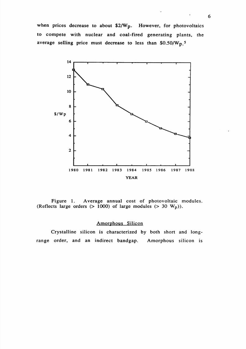
Figure 1 shows the yearly decline in photovoltaic module cost
which is down from $13AVp in 1980, to $3.80AVp in 1988.5
When the selling price reaches $3AVp, solar cells become
cost effective with diesel motors in remote applications such as
irrigation and villag e power. Grid connected photovoltaic power
generation becomes economically viable for supplying peakpower
8/8/2019 An Electron-cyclotron-resonance Plasma Apparatus For
http://slidepdf.com/reader/full/an-electron-cyclotron-resonance-plasma-apparatus-for 14/79
when prices decrease to about $2/W p. However, for photovoltaics
to compete with nuclear and coal-fired generating plants, the
average selling price must decrease to less than $0.50/Wp.5
$/Wp
1980 1981 1982 1983 1984 1985 1986 1987 1988
YEAR
Figure 1. Average annual cost of photovoltaic modules.(Reflects large orders (> 1000) of large modules (> 30 Wp)).
Amorphous Silicon
Crystalline silicon is characterized by both short and long-
range order, and an indirect bandgap. Amorphous silicon is
8/8/2019 An Electron-cyclotron-resonance Plasma Apparatus For
http://slidepdf.com/reader/full/an-electron-cyclotron-resonance-plasma-apparatus-for 15/79
non crysta lline and lacks long-range periodic ordering. There
exists however, short-range ordering up to the third and fourth
nearest neighbors which is approximately the same as that for
crystalline sili con. The short-range order is directly responsible
for observable semiconductor properties such as optical
absorption edges and activated electrical conductivities.
The lack of long-range order in amorphous silicon (a-Si) is
the con sequ ence of a very large density (lO^^ to 1020 cm-3) of
defects that exist primarily from broken bonds between the
silicon atom s. Th ese unsaturated or 'dangling' bonds correspond
to atoms missing neighbors at those sites where periodicity is lost.
As a result, even though the nearest neighbor configuration
is similar to that in crystalline silicon, the effect of disorder in
amorphous silicon has a profound influence on its electrical and
optical properties. The disordered atomic structure of amorphoussilicon causes the material to act more like an insulator than a
semicon ductor. The large defect density of gap states provides
fast nonradiative recombination centers that result in poor
electronic properties.
The high defect density in the gap of pure a-Si films makes
it impossible to change the position of the Fermi level byintroducing donor or acceptor type (e.g., phosphorus or boron,
resp ectively) dopants. This results from the fact that a change in
the position of the Fermi level requires a change of the state of
charge for an extrem ely large number of defect states. This
change in the state of charge cannot be compensated because the

8/8/2019 An Electron-cyclotron-resonance Plasma Apparatus For
http://slidepdf.com/reader/full/an-electron-cyclotron-resonance-plasma-apparatus-for 16/79
8
defect states act as t rapping centers for charged carr iers.
Therefore, the Fermi level is 'pinned' by the gap states in pure
amorphous si l icon.
Hydrogenated Amorphous Silicon Properties
The Role of Hydrogen
In order to effectively dope amorphous silicon, unpinning of
the Ferm i level is nece ssary. This is done by alloying the a-Si
with a passivating age nt. Hydrogen seems the most logical choice
for this pur pos e. The incorporation of hydrogen passivates bonds
that would otherwise be dangling bonds, thereby dramatically
reducing the density of localized states (DOS) in the gap.
Hydrogenated amorphous silicon (a-Si:H) has a DOS less than 10^6
c m " 3 e V - l , which is a density of defects as low as that found in
good quality single crystal semiconductors.
The low density of localized states in a-Si:H produces
desireable device properties, including a relatively long minority-
carrier diffusion length. W ith passivation of the dangling bonds,
doping of the material can be carried out to produce p-type and
n- type semiconductors .
Bandgap and Carrier Transport
The nature of a-Si :H puts certain l imitat ions on the
elect ronic proper t ies which are not present in crys tal l ine
sem icond uctors. This is due to the disordered atomic structure

8/8/2019 An Electron-cyclotron-resonance Plasma Apparatus For
http://slidepdf.com/reader/full/an-electron-cyclotron-resonance-plasma-apparatus-for 17/79
inherent in amorphous materials but which is absent in the
periodic array of atoms of a crystal.
Energy band theory successfully predicts the semiconductor
properties of crystall ine solids in terms of the conduction and
vale nce energ y ban ds, Ec and Ey in Figure 2(a). These bands
describe the number of quantum states at each energy that
electron s and holes can occupy. The bands correspond to energies
where the densities of states that the electrons and holes can
occupy are high, and the charge carriers in these 'extended' or
'nonlocal ized ' s tates can move freely through the material .
Between the conduction and valence energy bands, the density of
states drops to zero, so that no electrons or holes with energies
that wo uld be in the band gap can exist. This results in the we ll-
know n sem icondu ctor 'forbidden gap' or 'band gap.' The periodic
nature of crystalline material allows the charge carriers to have
large mean free paths, which results in high minority carrier
mobilities of the electrons and holes.
The atomic disorder inherent in amorphous semiconductors
causes d is t inct d i f ferences between them and crys tal l ine
m ateria ls. The absen ce of long range order introduces many
imperfect ions, so that the carr ier mean free paths becomesignifican tly low er than in the crys talline m ater ials. W hen the
disorder increases to the extent that the mean free path is
approximately equal to the interatomic distance, the charge
car riers bec om e localize d. The energy at which the mean free
path approximately equals the interatomic distance is called the
8/8/2019 An Electron-cyclotron-resonance Plasma Apparatus For
http://slidepdf.com/reader/full/an-electron-cyclotron-resonance-plasma-apparatus-for 18/79
1 0
>
TBandgap
>
DefectStates
TailStates
(a) Density of States (cm '^eV'^) (b) Density of States (cm '^eV '^)
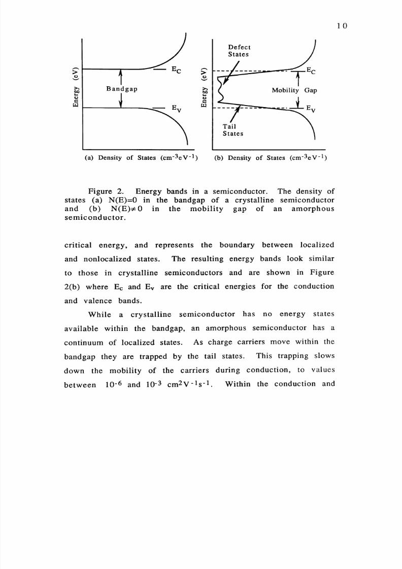
Fig ure 2. Ene rgy bands in a sem iconductor. The density ofstates (a) N(E)=0 in the bandgap of a crystalline semiconductorand (b) N(E):?tO in the mobili ty gap of an amorphoussemi co n d u c t o r .
crit ical energy, and represents the boundary between localized
and non localized sta tes. The resulting energy bands look similar
to those in crystalline semiconductors and are shown in Figure
2(b) wh ere Ec and Ey a re the critical energ ies for the conduction
and valence bands.
While a crystal l ine semiconductor has no energy states
available within the bandgap, an amorphous semiconductor has a
continuum of localized states. As charge carriers move within the
ban dga p they are trapped by the tail states . This trapping slows
down the mobility of the carriers during conduction, to values
betw een 10-^ and 10-3 cm ^V -^ s" !. W ithin the conduction and

8/8/2019 An Electron-cyclotron-resonance Plasma Apparatus For
http://slidepdf.com/reader/full/an-electron-cyclotron-resonance-plasma-apparatus-for 19/79
11
valence bands carrier transport occurs via extended states with a
much higher mob ility, 1 to 10 cm ^ V -l s' l, but significantly lower,
by a factor of 100 or more, than those in crystalline
semiconductors. So it is not the absence of states that give s rise to
the bandgap in an amorphous semiconductor but the very low
m obility within the gap. Therefore, the gap is more accurately
referred to as a mobility gap, and the carrier mobility is a trap
con trolled transport property. This low mobility limits the
applications of amorphous semiconductors to areas where speed is
not of importance.
Doping
The ability to dope a-Si:H is the critical component that
allow s it to be used in semiconductor devices. The low density of
midgap states allows the conductivity of hydrogenated amorphous
silicon to be modulated by doping. As in the case of crystalline
silic on , a-Si:H can be made n+ or p+ by the incorporation of
phosphorus or boron into the films. The doping efficiency in a-
Si:H is not as high as in crystalline silicon due to the
accompanyment of defects with the incorporation of dopants, and
the eventual pinning of the Fermi level by the tail states.Doping a-Si:H with boron or phosphorus alters the transport
properties, reduces the minority carrier diffusion length, and
increases the density of states in the gap. In a solar ce ll, heavy
phosphorus doping leads to a decrease in the open-circuit voltage
( V o c ) and to a lower short-circuit current density (Jsc)- The

8/8/2019 An Electron-cyclotron-resonance Plasma Apparatus For
http://slidepdf.com/reader/full/an-electron-cyclotron-resonance-plasma-apparatus-for 20/79
1 2
decrea se in both VQC and Jsc reduces the overa ll con ver sion
efficie ncy of the ce ll. Heavy boron doping has the deleterious
effect of reducing the photoconductivity, by introducing a series
resistan ce. Here again, the cell conversion efficiency is sacrificed.
Nevertheless, the conductivities of intrinsic (undoped) a-Si:H of
10-8 to 10-12 i2 -l c m -l can be increased to - 10-2 Q -l cm -l thro ug h
doping.
Absorpt ion
The disorder and hydrogen content in a-Si:H makes its
optical properties quite different than those of crystalline silicon.
The absorption coefficient for amorphous silicon, in the
wavelength region corresponding to the solar spectrum, is an
order of magnitude higher than that for crystalline silicon.
The magnitude of the absorption coefficient depends uponwhether the semiconductor material used is amorphous or
crysta lline. For crystalline material, the absorption coefficient also
depends upon whether it is a direct or indirect semiconductor. In
an indirect gap semiconductor, such as crystalline silicon, the
probability of light absorption is much less than for a direct gap
semicondu ctor. An excited electron in an indirect semiconductormust go through a momentum change as well as an energy change
in order to reach the conduction band. For GaAs, which is a direct
gap semiconductor, an electron with energy equal to the bandgap
can make the transition from the valence band to the conduction
band without a necessary change in mom entum. This satisfies the

8/8/2019 An Electron-cyclotron-resonance Plasma Apparatus For
http://slidepdf.com/reader/full/an-electron-cyclotron-resonance-plasma-apparatus-for 21/79
1 3
conservat ion of momentum requirement , thereby giving direct
gap sem icondu ctors a much higher absorption coefficient. Since
amorphous s i l icon has no long-range order , the momentum
con serv ation rule does not apply. This results in a much larger
absorption coefficient for amorphous silicon.
The disordered structure in a-Si:H produces a larger optical
gap (- 1 .7 eV) than in crystalline silicon (-1 .1 eV). This allows a-
Si:H films to absorb a significantly greater amount of light in a
com parab le thickness. This means that an a-Si:H fllm needs a
layer less than 1 j im thick to abso rb solar rad iat ion at
w av elen gth s less than 0.7 j im , while i ts crystall ine coun terpart
needs a layer more than 20 times as thick. Therefore, amorphous
silicon, unlike crystalline silicon, can be used to make thin-film
solar cells.
The two most important mechanisms for the absorption of
light by a semiconductor are the excitation by a photon of an
electron from the valence band to the conduction band and
trans itions within a band . The first mechanism, referred to as the
fundamental absorption, converts radiation into free electrons and
holes when a photon of ene rgy, equal to the energy gap Eg, i s
abso rbed. Only one electron-ho le pair is generated for a photonwith energ y large r than Eg . The exce ss ene rgy is dissipated as
thermal energy and contributes nothing to the conversion process.
The second process is referred to as free carrier absorption where
the energy of a free carrier is increased and not used in the
photovoltaic conversion process.

8/8/2019 An Electron-cyclotron-resonance Plasma Apparatus For
http://slidepdf.com/reader/full/an-electron-cyclotron-resonance-plasma-apparatus-for 22/79
1 4
An increase in the hydrogen content causes the optical gap
to increase and the corresponding absorption to decrease.
Therefore, a low hydrogen content is needed to optimize the
optical gap; whereas a rather high hydrogen concentration is
required to eliminate the dangling bonds and to obtain good
electronic properties. The opposite is true for doping. It has been
found that doping, with donors and especially with acceptors,
increases the absorption coefficient and decreases the optical
bandgap .
Hydrogenated Amorphous SiliconSolar Cell Structures
The Need For Photovoltaic Energy Conversion
In the not too distant future, renewable energy sources will
have to play a much larger role in meeting the world's energy
dem an ds. Solar energy is attractive sinc e it represents an
inexhaustible source, unlike depletable fossil fuels such as coal,
gas and oil . However, if solar energy is to be com petitive with
other methods of power generation, the cost must decrease and
the operating conversion efficiency increase.
The importance of solar cells cannot be understated; since
their potential for large-scale power generation, capable of
m eeting terrestrial energy requirements, is imm ense. Alm ost
everywhere on earth a typical house roof covered in solar cell
panels can supply enough electrical power for that household.
8/8/2019 An Electron-cyclotron-resonance Plasma Apparatus For
http://slidepdf.com/reader/full/an-electron-cyclotron-resonance-plasma-apparatus-for 23/79
1 5
The world's future population growth will occur in the third world
developing count r ies a long wi th an increased demand for
electr ical energ y. The world 's populat ion present ly stands at
approximately 5.5 billion, and will tower well above the 6 billion
m ark by ce ntury 's end. At that t ime , 40% of the wo rld's
population will live in rural villages inside third world countries,
where stand-alone electrical energy generation serves as the most
practical solution to the estimated future lack of centralized
gen eration. Solar energy may prove to be very attractive in such
s i t u a t i o n s .
From an ecological point of view, solar cells can help fulfill
the need for clean renew able energy resources. Clean renewables
can conceivably reduce the global warming effects due to
hydrocarbons , dramat ical ly decrease the conscious onslaught
against the world's forests, and extend the lifetime of the earth's
natural resources for generations to come.
Advantages of Amorphous Silicon Solar Cells
Amorphous sil icon solar cells have a number of distinct
advantages over their crystalline counterparts; these are listed as
fol lows:(i) Amorphous silicon has an absorption coefficient about
one order of magnitude greater than crystall ine sil icon in the
ma ximum solar energy wavelength region near 500 nm. This high
absorption coefficient allows a-Si solar cells to be constructed with
8/8/2019 An Electron-cyclotron-resonance Plasma Apparatus For
http://slidepdf.com/reader/full/an-electron-cyclotron-resonance-plasma-apparatus-for 24/79
1 6
an optically active region on the order of one micrometer thick,
instead of the necessary 20 jim for crystalline silicon.
(ii) Because less semiconducting material is needed in the
construction of amorphous sil icon solar cells, and the growth
temperature is low (200 to 400 °C), the energy requirements in
the manufacturing process are much smaller. This savings reduces
the energy pay-back period.
(i i i) Ine xp en sive sub strate m aterials such as glass or
stainless steel can be used to deposite amorphous silicon since the
semiconductor has a noncrystall ine latt ice structure.
(iv) The lack of long -rang e period ic order in am orphous
silicon allows greater control of physical constants such as the
energy gap.
(v) The ir fabrication processes are we ll suited to automa ted
large-scale, continuous, mass-production thin-film techniques.
Types of Solar Cell Structures
There are three basic types of amorphous silicon solar cell
structures, the Schottky barrier, the p-i-n, and the heterojunction.
The Schottky barrier solar cell has the simplest structure and
exh ibits reaso nab le con version efficiencies (5 .5 % )ii . It consists ofa transparent Schottky contact with a high work function, such as
platin um , on an intrinsic a-Si:H layer. Below the intrinsic layer is
a thin phosphorus doped a-Si:H layer deposited onto a metal
sub strate . The drawb ack with Schottky barrier cells is that they
severely degrade in the presence of moisture, therefore causing

8/8/2019 An Electron-cyclotron-resonance Plasma Apparatus For
http://slidepdf.com/reader/full/an-electron-cyclotron-resonance-plasma-apparatus-for 25/79
17
stability problems. Better cel l efficienc ies are realized with p-i-n
junctions and heterojunctions.
Doped hydrogenated amorphous silicon exibits extremely
sm all mino rity carrier lifetim es. This is due to the large
concentration of defects incurred during doping . Therefore, p-n
junctions do not exhibit good conversion efficiencie s. To obtain
better cells, the addition of an intrinsic a-Si:H layer, in a p-i-n
con figura tion, is used . The intrinsic layer is approximately fifty
times as thick as the p and n regions. The low density of gap
states (< 1 0 l6 cm -3) in the intrinsic layer allow s the junction to
have a large depletion width with a high minority carrier lifetime.
Most of the light absorption occurs in the intrinsic layer
generating more carriers to participate in the conversion process.
In p-i-n device construction, a transparent conductive oxide
(TCO) such as indium tin oxide (ITO) is deposited onto a glass
substrate. In order to increase light utilization and thus the cell's
current, the surface of this film is textured. ^ Texturing reduces
the optical reflection of the incoming sunlight and increases the
optical path length in the material. The ITO film is followed by a
thin boron doped layer (10-30 nm), an intrinsic layer (300-600
nm), and a phosphorus doped layer (10 -30 nm ). The structure iscompleted with the deposition of a metal reflector/contact, such as
silver or aluminum. Although p-i-n cel ls exhibit efficien cies at or
above 6%, a boron doped top layer is not very appropriate
beca use of the material's large absorption coe fficien t. The
extremely short minority carrier lifetime inherent in this layer

8/8/2019 An Electron-cyclotron-resonance Plasma Apparatus For
http://slidepdf.com/reader/full/an-electron-cyclotron-resonance-plasma-apparatus-for 26/79
18
will also de gra de the cells efficiency. The se effects d rastically
reduce the convers ion ef f ic iency, especial ly in the shor t
wavelength range.
The problems with the p-type layer are corrected by
replacing it with a hydrogenated amorphous silicon carbide film
(a-S iC:H ). Since the carbon doped film has a different bandg ap
than intrinsic a-Si:H, a heterojunction is formed at the interface.
Carbon alloyed a-Si:H is a wide bandgap material (1.9 eV) that is
transp aren t to inciden t light. The layer increases the open-circuit
voltage of the solar cell by reducing carrier recombination at the
p-i junction.
Figure 3 illustrates two types of a-Si solar cell structures.
The p-i-n cell is the most common structure used in commercial
pro du cts. Th e heterojunc tion solar cell shown in figure 3(a) is
fabricated by first depositing a thin silicon-dioxide (Si02) buffer
layer on glass, and then depositing a 600 nm thick transparent
con duc ting oxide layer of tin-oxide (S n0 2) . This textured layer
enhances l ight trapping over the visible wavelength range and
red uce s the series resis tanc e of the cell structu re. The p-type
layer (10 nm) is a boron doped wide bandgap a-SiC:H film. The
intrinsic a-Si:H layer is typically 250-500 nm thick with a slightamount of boron doping to allow for better intrinsic behavior
unde r illum inatio n. The n-type layer is a pho spho rus doped a-
Si:H film about 20-30 nm thick. The rear contact is an evaporated
or sputtered alum inum . M anufacturers have achieved conversion

8/8/2019 An Electron-cyclotron-resonance Plasma Apparatus For
http://slidepdf.com/reader/full/an-electron-cyclotron-resonance-plasma-apparatus-for 27/79
19
h\)
Glass
SiO.SnO,
a-SiC:H
a-Si:H
n
(a)
h\)
\ic SiC:H
a-Si:H
jxc Si:H n
(b)
Figure 3. Schem atic diagram of a-Si:H solar ce lls , (a)Heterojunction structure with boron doped p-layer, andpho sohor us doped n-layer. (b) p-i-n structure with dopedm icrocry stalline (|ic) n and p layers.

8/8/2019 An Electron-cyclotron-resonance Plasma Apparatus For
http://slidepdf.com/reader/full/an-electron-cyclotron-resonance-plasma-apparatus-for 28/79
2 0
efficiencies of 12% by replacing the rear aluminum contact with
an ITO/silver contact.^
Another commercially used amorphous sil icon structure is
that shown in Figu re 3(b). The substrate is stainless steel foil with
both the n-layer and p-layer doped microcrystall ine ( | ic) Si:H.
This configuration produces a flexible solar cell commonly found
in cred it card -size calc ulato rs. Ano ther flexible a-Si structure is
show n in Fig ure 4. In this ca se, two p-i-n structures are stacked
in tande m . The thicknesses of the a-Si:H layers are adjusted so
that the curre nts from the two cells are similar. For large-area
modules, the fi lms are patterned to series-connect the cells as
shown in Figure 5.
h\)
• • i r r o .^c SiC:H
a-S i :H
^ic Si:H
^ic SiC:H
a-S i :H
^ic Si:H
Is ta inless s tee l !
P
i
n
P
Figu re 4. Stacked p-i-n type heterojunction structure.

8/8/2019 An Electron-cyclotron-resonance Plasma Apparatus For
http://slidepdf.com/reader/full/an-electron-cyclotron-resonance-plasma-apparatus-for 29/79
2 1
M e t a l
a-Si:H
(p-i-n)
Glass Substrate rro
Figure 5. A large-area series-conn ected hydrogenatedamorphous silicon solar cell array.
Conversion efficiencies of 13.7% and 15.6% have been
obtained in multijunction laboratory cell structures that utilize a
narrow bandgap layer (a-SiGe:H:F and CdS/CuInSe2 layers,
respectively) to increase the collection efficiency in the red and
near infrared region . Since a-Si:H has a bandgap of about 1.7 eV,
most of the incident infrared radiation is passed through this
layer. Varying the concentration of germanium from 0 to 100%,
the optical bandgap of a-SiGe:H can be changed from 1.7 to 1.1 eV.
Unfortunately, only low levels of germanium can be incorporated
before the alloying seriously deteriorates the electronic properties
of the material. This deterioration is also common to carbon alloys
with high levels of doping. As a result, a-Si:H alloy solar cells can

8/8/2019 An Electron-cyclotron-resonance Plasma Apparatus For
http://slidepdf.com/reader/full/an-electron-cyclotron-resonance-plasma-apparatus-for 30/79
2 2
be fabricated with good electronic properties having optical
bandgaps between 1.45 and 1.9 eV.i3
Solar Cell Conversion Efficiency
There are several conditions that must be satisfied for
amorphous silicon solar ce lls to operate efficien tly. First, the
optical absorption coefficient must be sufficiently large to absorb
a significant fraction of the solar energy in the film. For films on
the order of 1 jim in th ickness, the absorption co efficient, a , must
be greater than 10^ cm-1 over at least the visible portion of the
solar spectrum. Second, the photogenerated electrons and holes
must be efficiently collected by contacting electrodes on both
sides of the semiconductor film. This implies that the minority
carrier diffusion length be comparable to the film thickness.
Third, a large built-in potential is necessary since it determines
the output vo ltage of the ce ll. This potential is generated by the
formation of a semiconductor junction such as a heterojunction, a
p-i-n junc tion , or a Schottky barrier. Fina lly, the total solar cell
series resistance must be kept small so that the IR drop is a small
percen tage of the output vo ltag e. Contributions to the series
resistance come from the bulk resistivity, the contacts, the currentcollection grids, and the electrical wiring.
The conversion efficiency of a solar cell is defined as the
ratio of the maximum electrical power (Pm) to the power of the
incident light (Pi), both measured in Wcm -2. The equation can be
written as

8/8/2019 An Electron-cyclotron-resonance Plasma Apparatus For
http://slidepdf.com/reader/full/an-electron-cyclotron-resonance-plasma-apparatus-for 31/79
23
- _ J n . V n , _ ( F F ) J s c V o c
^ Pi Pi • ^'^
where Jm and Vm are the output current density and voltage for a
cel l operating under maximum output power co nditions, and Pi is
the total power incident on the cell ( P i» 100 mW cm-2 for the sun
directly overhead on a clear day; AM I cond ition). Jsc is the short
circu it current dens ity of the cel l, and VQC is the open circuit
voltage of the ce ll. The fill factor (FF) is defined by
(FF) = imYm_, (2 )J sr V /'SC ^ OC
with a theoretical achievab le value as high as 0.8 5. However,
series resistance effects will lead to considerably lower fill factors
of less than 0.75.
Several authors have estimated a theoretical limit on the
con versio n efficien cy for a-Si:H solar ce lls.i^ The maximum
con versio n efficien cy is found to be approximately 18%. The
upper limits for the three factors that determine the conversion
efficiency where calculated to be V oc « l V, Jsc=22 m Acm -2, and
F F «0.8 0 . Higher efficienc ies are possible if the density of states is
reduced .

8/8/2019 An Electron-cyclotron-resonance Plasma Apparatus For
http://slidepdf.com/reader/full/an-electron-cyclotron-resonance-plasma-apparatus-for 32/79
2 4
Stabil i ty
Optical degradation is the most important obstacle to
overcome if a-Si:H solar cells are to become a promising energy
sou rce. This degradation is known as the Staebler-W ronski
e f f ec t . 15 It is a phenomenon, common to all amorphous silicon
allo ys , of l ight- induced photoc ondu ctivity decrease. This
phenomenon seems to originate from the breaking of weak Si-Si
bonds by nonradiat ive recombinat ion of photogenerated
carriers. 16-18 The breaking of weak bonds creates a large number
of metastable dangling bonds that degrade the cells
pho tocon duc tivity. This degradation seems to be self-limiting
though, since the number of created dangling bonds will saturate
and cause the collection width to decrease and saturate to a
smaller value.
Therefore, the degradation problem can be circumvented to
a point by keeping the device thickness approximately equal to
the smallest co llectio n width attained. Another means of reducing
the degradation effects is to keep impurities, such as oxygen and
carbon, below 10+20 cm-3 in the intrinsic layer. Stability problems
tend to improve by increasing the deposition temperature, and
decreasing the hydrogen content, i'*
Conclusion
Thin film a-Si:H solar cell structures are rapidly closing the
gap in becoming a viab le alternative energy source. In the last
decade, the overall cost to manufacture a-Si:H solar cell modules

8/8/2019 An Electron-cyclotron-resonance Plasma Apparatus For
http://slidepdf.com/reader/full/an-electron-cyclotron-resonance-plasma-apparatus-for 33/79
2 5
has steadily declined (presently les s than $3.80/W p). During this
same period, the efficiencies for small-area laboratory cells (1-
cm 2) have been reaching the theoretical limit. The manufacturing
cost still needs to drop to about $2/Wp in order for utility-scale
power generation to be eco nom ically practical. Even though
laboratory cells have shown high conversion efficiencies, large
power modules (1 m2) have only achieved stable efficiencies of
6%. Therefore, improvem ents in manufacturing techniques are
still needed with future research directed at a better
understanding of the physics underlying film deposition and
growth .
Several key areas have been identified as vital to the
successful development of amorphous silicon thin-film solar cells.
The first area involves improved device quality through careful
material preparation, tight processing control, and state-of-the-arthigh vacuum equipment and techniques to reduce contamination.
The second area is the development of high-quality small bandgap
films using amorphous silicon-germ anium allo ys . A third
important issue is amorphous thin-film deposition kinetics. This
requires an understanding of particle bombardment and
deposition parameters on the film's electronic properties.Improved processing parameters are needed to reduce the
number of localized states in the gap and to decrease the tail-state
effe cts. A fourth is the deve lopm ent of numerical models to
simulate dev ice behavior. This will allow the ability to analyze
thin-film solar ce lls without constructing com plete devic es. The

8/8/2019 An Electron-cyclotron-resonance Plasma Apparatus For
http://slidepdf.com/reader/full/an-electron-cyclotron-resonance-plasma-apparatus-for 34/79
2 6
final, and major area of concern, is the improvement of long-term
device stability. The fundamental issue here is the light-induced
photocond uctivity degradation or Staebler-Wronski effect. An
improved overall understanding of the physics behind the
material is necessary if amorphous silicon is to become a practical
alternative energy source.

8/8/2019 An Electron-cyclotron-resonance Plasma Apparatus For
http://slidepdf.com/reader/full/an-electron-cyclotron-resonance-plasma-apparatus-for 35/79
CHAPTER III
BASIC ELECTRON-CYCLOTRON-RESONANCE
PLASMA THEORY
I n t r o d u c t i o n
M i c r o w a v e e l e c t r o n - c y c l o t r o n - r e s o n a n c e ( E C R ) p l a s m a
discharges have become an area of increasing interest due to their
use in many plasm a processing applications. Electron cyclotron
resonance (ECR) plasmas have been utilized for the last 25 years
in vario us fields of plasm a techn ology . This techno logy, borrowed
from fusion!9 and electric propulsion plasma,20 has developed into
an attractive plasma discharge process relevant to semiconductor
m anu factu ring. This technology offers a num ber of desirable
cha racteristics, including high plasma densities (=1 0^^-1 0!^ c m '^ ),
high degree of ionization (10% and higher), electrodeless nature,
low gas pressures (lO'^^-lO'-^ Torr), compatibility with active and
corro sive gas es, and stability of operation. Another imp ortant
feature is the abili ty to produce high-quality fi lms at low
deposi t ion temperatures .
The low-temperature and low-pressure microwave ECR
plasma process i s becoming at t ract ive for use in many
semiconductor applications, and constitutes a possible means of
me eting stringent processing requirem ents. Although microwave
ECR plasma systems are being increasingly used for thin-film
deposition, similar systems, for other uses, have been developed;
e.g., plasm a stream and reactive ion beam etching,2i sputtering -
2 7

8/8/2019 An Electron-cyclotron-resonance Plasma Apparatus For
http://slidepdf.com/reader/full/an-electron-cyclotron-resonance-plasma-apparatus-for 36/79
2 8
type ECR plasma deposition,22 ion implantation,23 and diamond-
film prod uction .24 The movem ent towards smaller, faster, more
densely packed semiconductor devices has spurred a need for
mo re accu rate processing techniques. In order to improve these
techniques for both etching and deposition, better uniformity,
lower damage levels for thinner structures, and lower deposition
temperatures are needed, while still yielding high quality films at
h igh throughputs .
Various types of films have been deposited using microwave
ECR plasm a disc har ges . The general trend is that films can be
deposited at lower temperatures than for CVD or conventional
plasma-CVD processing, with comparable or better fi lm quality.
Although deposition rates are generally low, progress has been
made in scaling these upward through higher flow rates and
greater microwave power.
Microwave ECR Breakdown
ECR plasma absorption occurs when microwave energy is
coupled to the natural resonant frequency of electrons in the
pre sen ce of a static magn etic field. In any gas there is a small
number of electrons present due to ionization by cosmic rays orsome other phe nom eno n. W hen the electron cyclotron frequency
in a magnetic field, which is defined as
0)ce=eB/me, (3)

8/8/2019 An Electron-cyclotron-resonance Plasma Apparatus For
http://slidepdf.com/reader/full/an-electron-cyclotron-resonance-plasma-apparatus-for 37/79
2 9
(where e = electron charge, B = static magnetic flux density, and
m c = electron ma ss) equals the m icrowave excitation frequency
(co), reson ance occurs. This resonance efficiently transfers energy
from the electromagnetic field to the electrons. The ECR coupling
takes place within a small, thin volume, commonly known as an
ECR layer . W ithin this layer most of the applied power is
absorbed; producing high-energy electrons necessary to sustain a
discharge at low operating pressure. The accelerated electrons
move out of the ECR layer throughout the discharge volume
collisiona lly d issociating and ionizing the neutral gas. The result is
a low-pressure, almost collisionless, plasma that can be varied
from a weakly to a highly ionized state by changing discharge
pressure, gas flow rates, and input microwave power.25
For a standard 2.45-GHz magnetron the corresponding static
magnetic field needed is 0.087 5 T. Several reasons have made2.45 GHz the frequency utilized in all the ECR processing work
reported to date. The magnetic field required for resonan ce at
this frequency is relatively easy to obtain with ordinary water-
coo led solenoid al electrom agnets. The magnetron, hardware and
power supplies are readily available for this operating frequency.
The densities obtained are high enough to be useful in presentmaterials processing applications.

8/8/2019 An Electron-cyclotron-resonance Plasma Apparatus For
http://slidepdf.com/reader/full/an-electron-cyclotron-resonance-plasma-apparatus-for 38/79
3 0
Microwave ECR Energy Coupling
Energy Transfer
In an arbitrary microwave plasma discharge, the energy
from the electromagnetic field is absorbed by both the electron
and ion g as. In most cases though, direct energy transfer to the
ion gas can be neglected (except for ion cyclotron resonance) due
to the low m obility of the ions. This is because the work imparted
to a charged particle by an electric field varies inversely with the
particle mass.
Ions can still have an effect on plasma dynam ics. As
electrons are extracted from the discharge region, primarily along
the magnetic field lines, an electrostatic potential is created that
tends to pull positive ions in the same direction. Although direct
energy transfer is negligible in an ion gas, ions do undergo circular
Larmor gyration about the magnetic field line s. However, the
greater mass of the ions causes them to have an orbital radius
much larger than that of the elec trons. For an argon ion having
kinetic energy of 5 eV transverse to a magnetic field of 0.0875
Tesla, the Larmor radius is about 23 mm (as compared to 0.1 mm
for an electron). This large orbital radius will cause the ion gas to
loose most of its energy through collisions with the chamber walls.For an ECR discharge, the electron gas is excited directly by the
microw ave electric field. The electrons continuously gain energy
and are accelerated . Neutral and ion gases acquire energy by way
of co llis io ns with the heated electron gas. This ECR energy
transfer process for a discharge volume is shown in Figure 6.

8/8/2019 An Electron-cyclotron-resonance Plasma Apparatus For
http://slidepdf.com/reader/full/an-electron-cyclotron-resonance-plasma-apparatus-for 39/79
3 1
RadiationLosses
DischargeContainer
Wall
Joule Heatingand ICRHeating
MICROWAVEELECTRIC
FIELD
Elasticand
InelasticCollisions
RadiationLosses
HeatConduction
andConvection
Figure 6. Microwave energy transfer in a discharge v o l u m e .

8/8/2019 An Electron-cyclotron-resonance Plasma Apparatus For
http://slidepdf.com/reader/full/an-electron-cyclotron-resonance-plasma-apparatus-for 40/79
3 2
Through the interaction with the electron gas, the neutral
and ion gases interchange energy by way of collisions, and
transfer energy to the walls through heat conduction and
conv ect ion . Therefore, los ses from the discharge have a direct
dependence upon the electron density, pressure, gas type, and
discharge geometry.
Power Absorption in a Magnetic Field
Without the presence of a static magnetic field, a plasma
discha rge is pressure depend ent. There fore, at low pressures
(<100 mTorr), it is difficult to sustain a discharge without high
applied electric field s. With the addition of a static magnetic field
high power absorption, even for very low applied electric fields, is
easily obtained.
The equation of motion of an electron will now be used to
study the absorbed microwave power in both cases, with and
without a static magnetic field. Newton's law along with an added
term that represents the momentum loss of the electron due to
collisions with ions and neutrals is known as the Langevin
equation and is given by
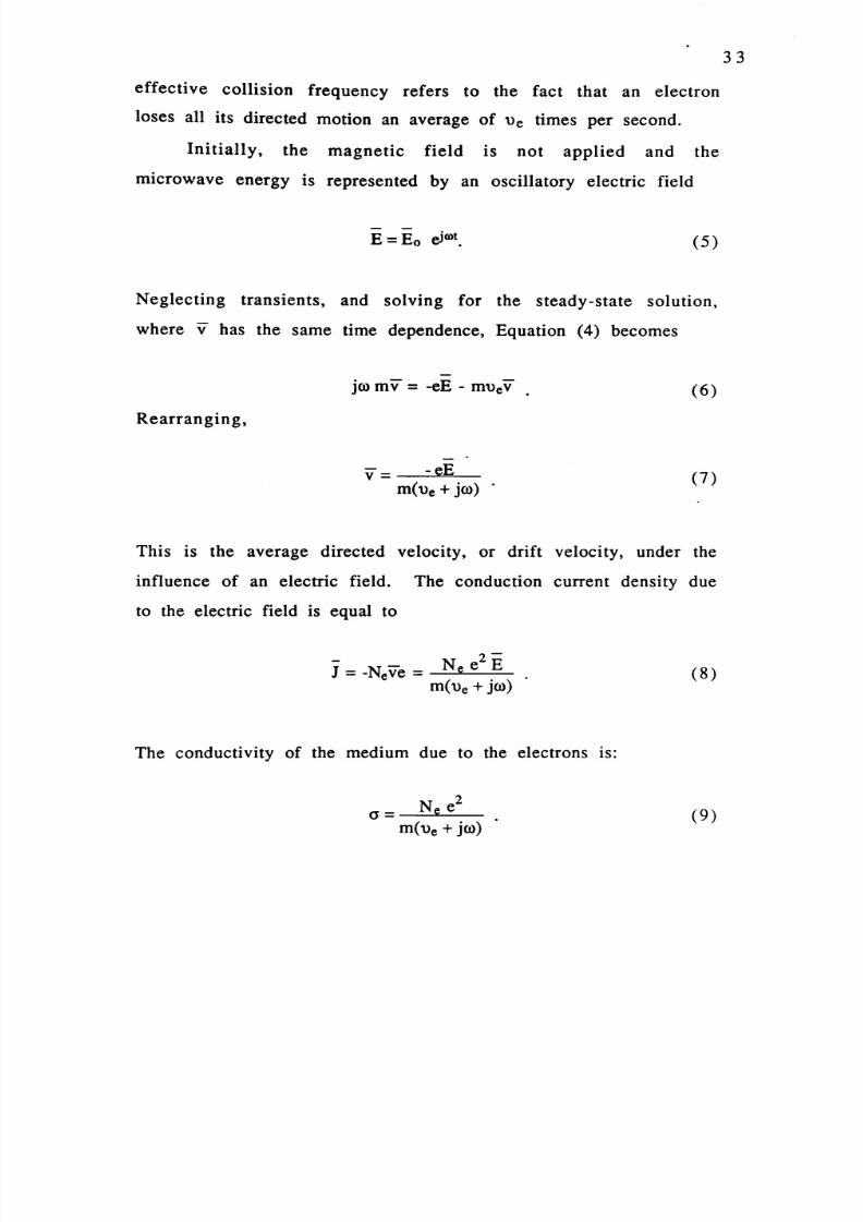
- ^ mv" = -e [E + v" X B] - m\)eV , (4 )dt
where v" is the average directed ve loci ty, e is the electron charge,
and x>c is the effectiv e collis ion frequency for electrons. The
8/8/2019 An Electron-cyclotron-resonance Plasma Apparatus For
http://slidepdf.com/reader/full/an-electron-cyclotron-resonance-plasma-apparatus-for 41/79
33
effective coll ision frequency refers to the fact that an electron
loses all its directed motion an average of De times per second.
Init ia l ly , the magnetic f ie ld is not applied and the
microwave energy is represented by an oscillatory electric field
E = Eo ei ^ (5 )
Neglecting transients, and solving for the steady-state solution,
wh ere v" has the same time depen dence. Equation (4) beco m es
jco m v = -eE - m-OgV . ( 6 )
R e a r r a n g in g ,
v = -fiE ( 7 )m(\)e-i-jo))
This is the average directed velocity, or drift velocity, under the
influenc e of an electric field. The condu ction current density due
to the electric field is equal to
J = - N e 7 e = ^ ^ ^ E . ( 8 )
m(\)e + jco)
The conductivity of the medium due to the electrons is:
^^ __ N £_ e ^ ^^^
m(\)e + jco)
8/8/2019 An Electron-cyclotron-resonance Plasma Apparatus For
http://slidepdf.com/reader/full/an-electron-cyclotron-resonance-plasma-apparatus-for 42/79
3 4
The conductivity and the applied electric field is now used to
write the expression for the absorbed power density for the
electron gas as
Pabs = R e ( a ) E ^ ( 10 )
w here R e (a ) is the real part of the conductivity, given by
R e(a) = N ^ ( V " ) ( 1 1 .
This term for the conduct iv i ty shows the expl ic i t
dependence of the absorbed power on vjod. With the density and
electric field held constant. Equation (11) has a maximum when
co^De- Th e effective collision frequency, VQ, varies directly with the
gas pre ssu re. For the case of hyd rogen, \)e ~ 4.9 x lO^p, where p =
gas pres sure in Torr at 300 K. Therefore, maximum microw ave
power absorpt ion is discharge-pressure dependent , and good
microwave energy coupling is possible in a coUisional heating
p r o c e s s .
For very low pressures, <100 mTorr, the mean free path
between electron-neutral and electron-ion collisions becomes very
long, \)e«co, and Equation (10) becomes
Pabs = ^ (VCO) E^ • (^2 )

8/8/2019 An Electron-cyclotron-resonance Plasma Apparatus For
http://slidepdf.com/reader/full/an-electron-cyclotron-resonance-plasma-apparatus-for 43/79
3 5
In order to sustain a discharge at low operating pressures, and
without the presence of a static magnetic field, high plasma
de nsitie s and high applied electric fields are requ ired. W ith the
inclusion of an ECR static magnetic field the discharge process is
greatly simplified.
With the field included, the complete steady-state Langevin
equation is given as
(De-Hjco)m \r=-e [E + v"x B] . (1 3 )
For the simple case where the electric field is perpendicular to the
static magnetic field, the absorbed power by the electron gas
b e c o m e s
P a b s = ^ ^ f ^ [ ^ - + 1 - ] E ^ . ( 1 4 )2 m ^ 2 + (co-COce) 'Ol + (cO+COce)
If the collision frequency is reasonably small with respect to the
frequency of the applied electric field, a)e<<co, Equation (14)
b e c o m e s
P a b s = ^ ^ ^ [ 1 - ] E ' . (1 5 )2 m ^ 2 + (co-COce)
Equation (15) will peak in a resonant manner if the frequency of
the appl ied electr ic f ield approaches the electron cyclotron

8/8/2019 An Electron-cyclotron-resonance Plasma Apparatus For
http://slidepdf.com/reader/full/an-electron-cyclotron-resonance-plasma-apparatus-for 44/79
3 6
freq uen cy (co=coce). This indicates a high pow er absorption even
with very low impressed electric fields.
This is the ECR condition under which the motion of an
electron in the magnetic field is in synchronization with the
applied osc illato ry electric field. An elec tron with co=(Oce will feel
the us ual Lo ren tz force ev X B and begin to drift in the direc tion
norm al to E and B . This is the well known electric field drift, V E ,
and is illustrated in Fig ure 7(a). In the first quarter cycle of the
electron's orbit, the electron will gain energy from the increasing
electric field, and accelerate in the plane normal to the magnetic
field. Th e elec tron's La rmo r radiu s is increa sing at this time.
During the second quarter of the orbit, when the electric field is
decreasing, the electron will also accelerate, but at a lower rate
than it did du ring the first qua rter cy cle . Th e final half orbit
produces the same effects only in the opposi te direct ion.
Therefore, at ECR, an electron is subject to continuous acceleration
by the elec tric field. Electron s with the "right" phase will gain
energy; whereas electrons with the "wrong" phase wil l lose
ene rgy. The motion that the electron makes is shown in Figure
7(b). The increasing orbit and speed of the electron is limited by
a collision with another particle, a collision with a wall , or
movement out of the ECR region.
It should be noted, however, that as the discharge pressure
incre ase s, pure ECR heating gives way to collisional heating. As
the pre ssu re is increased the collisional frequency -Oe app roa che s
8/8/2019 An Electron-cyclotron-resonance Plasma Apparatus For
http://slidepdf.com/reader/full/an-electron-cyclotron-resonance-plasma-apparatus-for 45/79

8/8/2019 An Electron-cyclotron-resonance Plasma Apparatus For
http://slidepdf.com/reader/full/an-electron-cyclotron-resonance-plasma-apparatus-for 46/79
3 8
the magnetic field has little influence on the heating of the
electron ga s. Therefore, ECR is a coup ling technique for low -
pressure discharges where the electrons can orbit many times
between collisions, or at least Ve^coce-
Magnetic Mirror Effects
Most ECR plasma discharge systems employ a nonuniform
static magnetic field comm only known as a magnetic mirror. The
name refers to the fact that this field configuration can reflect
charged particles entering a high-field region . Therefore, a pair of
co ils that form two magnetic mirrors can confine a plasma. This
effect works both on ions and electron s. Figure 8 illustrates this
scheme where the magnetic field is highest in the throat (Bm) and
wea kest at the midplane ( B Q ) . A magnetic mirror is produced
either by permanent magnets or magnetic coils.
B
Figure 8. Plasma confined between magnetic mirrors.
8/8/2019 An Electron-cyclotron-resonance Plasma Apparatus For
http://slidepdf.com/reader/full/an-electron-cyclotron-resonance-plasma-apparatus-for 47/79
3 9
The basis for plasma confinement in a magnetic mirror is
the invariance of the magnetic moment, ^i. The magnetic moment
for a gyrating particle is defined as
i =4 -m v// B . (1 6)
As a particle moves into regions of stronger or weaker
fields, its Larmor radius changes, but ji has to remain constant.
Therefore, the particle's perpendicular velocity Vi must increaseduring periods of increasing magnetic field. Since energy must be
cons erv ed , the para llel ve loc ity v„ has to decrease. If the
magnetic field is high enough in the throat, the parallel velocity
will become zero; and the particle is reflected back to the weak-
field region.
In the absence of an electric field, a charged particle moving
into a converging field will spiral with ever decreasing transverse
orbits until it is reflected . The particle will then reverse direction
and spiral back into the weak-field region with increasing orbit.
When a transverse microwave electric field is present in the
magnetic mirror, acceleration of the electrons takes place when
they pass through the ECR region where co=o)ce- Outside this ECR
region, the electrons experience little or no energy absorption as
indicated from Equation (15); and will experience the usual mirror
force.

8/8/2019 An Electron-cyclotron-resonance Plasma Apparatus For
http://slidepdf.com/reader/full/an-electron-cyclotron-resonance-plasma-apparatus-for 48/79
4 0
Confinement of the plasma is not perfect. A particle with
Vi=0 will have no magnetic moment and feel no force in the
dire ction of the field . A particle with a small ratio of
perpendicular velocity to parallel velocity will also escape if the
maximum field at the throat is not large enough.
Conclusion
From the previous discussion, an ECR plasma offers a
number of desireable characteristics; the most notable being an
efficient means of producing high-quality films at low deposition
temperatures. The electr ode less and electron-cyclotron -heating
nature of the plasma is suitable for many processing applications.
The ECR plasma is easily maintained, even for very low applied
electric fields.
Because the ECR process accelerates high-energy electrons,
the electron energy distribution will be non -M axw ellian. This
makes the form of the distribution dependent upon the applied
electr ic field, and the size and shape of the ECR layer. Therefore,
the electron energy distribution can be controlled by the applied
electric field and the magnetic mirror configuration. This control
over the ECR plasma helps to slow down the electrons prior tostriking the substrate. This is favorab le since most plasma
processing applications do not desire high-energy electrons.

8/8/2019 An Electron-cyclotron-resonance Plasma Apparatus For
http://slidepdf.com/reader/full/an-electron-cyclotron-resonance-plasma-apparatus-for 49/79
CHAPTER IV
SYSTEMLAYOUT
ECR Apparatus
A schematic diagram of the ECR plasma deposition apparatus
is show n in Figu re 9. The ultra-high-vacuu m system is made
entirely of stainless steel. The discharge chamber, with an inside
diameter of 13.3 centimeters, is located inside two sets of magnet
coils. The magnet coil current is supplied by a Hobart type M-600
dc m otor-g ene rator arc we lder. The coils are used to provide a
m agn et ic f ield in a dual magn et ic mirror configurat ion; a
magnitude plot of the field along the chamber axis is shown in
Fig ure 10. The axial m agn etic field strength is adjusted so that
the field is greater than the ECR value at the coil locations, and
decrea ses with axial position as shown. Positioning the microwave
input to the chamber at the location of the left coil set, places the
waveguide window in the region of greatest magnetic field
inten sity. Th is pos itions the intense ECR layer away from the
waveguide window.
Microwave power is generated by a 2.45 GHz continuous-
wave power source (with a Matsushita 2M137 magnetron) and
int roduced in to the d ischarge chamber v ia a rectangular
wa vegu ide and quartz vacuum window . The incident microwave
pow er can be continuously varied up to 1 kW . The incident power
Pine and reflected power Pref are both measured using a dual
directional coupler and power meters.
4 1
8/8/2019 An Electron-cyclotron-resonance Plasma Apparatus For
http://slidepdf.com/reader/full/an-electron-cyclotron-resonance-plasma-apparatus-for 50/79
4 2
os D > ...C/3
3«->
h icd
a.
ao
O
a.
u
c
a.X
e
oCO
ON
(1 1
300

8/8/2019 An Electron-cyclotron-resonance Plasma Apparatus For
http://slidepdf.com/reader/full/an-electron-cyclotron-resonance-plasma-apparatus-for 51/79
4 3
1000
>^
•-3 C
o QI s
^ X = ^ V - ECR
0
MicrowaveSource
10
MagnetCoi l s
20 3 0 Distance (cm)
Langmuir probes
SampleHolder
Viewpor t
Fig ure 1 0. M agnitud e plot of axial m agnetic field alignedwith m icrowa ve ECR deposition system. The peak to minimumratio is 1.3. M agnitude plot provided by a magnet coil current ( I B )of 300 A.
A four-stub tuner is used to match the ECR discharge load
for different disc harg e co nditio ns. A unique feature of the
microwave system is the use of a three-port circulator and
dummy load as an attenuator instead of an isolator.
A circulator is designed to protect the magnetron from large
reflected power conditions that could damage or shorten the life
of the de vic e. The three-p ort circu lator is norm ally configured

8/8/2019 An Electron-cyclotron-resonance Plasma Apparatus For
http://slidepdf.com/reader/full/an-electron-cyclotron-resonance-plasma-apparatus-for 52/79
4 4
with the microwave input at port 1, the discharge load at port 2,
and a matched dummy load at port 3 . In this arrangement, all the
power entering port 1 leaves port 2, and all the reflected power
from the nonlinear plasma load exits port 3 into the matched
dumm y load . Th is isola tes the magnetron from the nonlinear
discharge and allows it to operate into a matched load
indepen dent of discharge variations. The drawback for this
configuration occurs when trying to operate the magnetron at
output pow er lev els below 50 W atts. Be low this value, magnetron
operation is unstable with similar consequences for the plasma
discharge. Since the plasma deposition process needs power in
the range of 10 to 50 Watts, some method of providing stability is
n e e d e d .
In the method we have chosen, the circulator and dummy
load are configured as an attenuator, with the connections to ports
2 and 3 interchanged and a stub tuner added with the dummy
load (see illustration in Figure 9). This allows the magnetron to
operate at high powers (5 00 W ) where its output is stable. A
portion of the applied power to the dummy load is reflected by
the stub to the discharge chamber. This allow s low m icrowave
power, in the range of 0-50 Watts, to be applied to the dischargechamber withou t magnetron instability problem s. Adapting the
microwave system in this manner produces a controllable, stable
discharge for different operating conditions.
Numerous flanges and viewports provide locations for the
connection of gas pressure gauges, Langmuir probes, gas input.

8/8/2019 An Electron-cyclotron-resonance Plasma Apparatus For
http://slidepdf.com/reader/full/an-electron-cyclotron-resonance-plasma-apparatus-for 53/79
4 5
and discharge observat ion windows (viewports) as shown in
Figu re 9. Tw o MK S type-1159B m ass flow controllers are used to
maintain a prescribed flow for the hydrogen and liquid-source
gases in units of standard cubic centimeters per minute (SCCM).
Argon and helium are connected at the other two inputs, and are
used as inert discha rges for cleaning and plasma diagnostics. The
gas f low rates for these inputs are cont ro l led by a
G ran vi l le /P hi l l ips var iab le leak valve. Single and double
Langmuir probes are used to measure radial profiles of the
plasma density and temperature at the two locations shown in
Figure 9.
Th e sam ple holder is located 15 centim eters dow nstream
from the right magne t coil set. Figure 11 (a) shows a detailed
draw ing of the samp le holder. It contains an electric heater that
can regulate the substrate temperature from room temperature to
425 °C . Th e holde r is electrica lly isolated from the cham ber and
can be kept at the floating potential or rf biased. A thermocouple
placed inside the holder is used to monitor the substrate
tem per atu re. A wa ter-cooled M axtek type TM-IOOR thickness
m onitor is located above the sam ple holder. The thickness
monitor provides a direct display, at high update rates, of filmthickn ess and depo sition rate during depo sition. This allows for
improved manual control of the vacuum film deposition process.
A manual shutter is used to cover the sample to prevent
depos i t i on dur ing d i scharge tun ing and af t e r comple ted
pro ces sing . A num ber of pilot holes are drilled in the holder to

8/8/2019 An Electron-cyclotron-resonance Plasma Apparatus For
http://slidepdf.com/reader/full/an-electron-cyclotron-resonance-plasma-apparatus-for 54/79
4 6
HEATERSHUTTERCaSTTROL \
THERMOCOUH^
BIAS
I • 1 1
SAMPLEPLUGPORT
4-^I I
c
CERAMICSPACERS
TOP VIEW
FRONT VIEW
(a)
SAMPLEPLUG
CRYSTALLINESILICON SUBSTRATE
l/4"xl/2" ea.
(b )
G L A S S
S U B S T R A T E
Figure 11 . (a) Sample holder show ing feedthroughconnections, (b) Sample plug showing substrate mounting.

8/8/2019 An Electron-cyclotron-resonance Plasma Apparatus For
http://slidepdf.com/reader/full/an-electron-cyclotron-resonance-plasma-apparatus-for 55/79
4 7
prevent outga sing from the internal cavities. Feedthroughs to the
sample holder are introduced through a six-way port (see Figure 9
for de tai ls). Sam ple insertion is performed by way of the load-
lock section and substrate feedrod.
Two substrates, one glass and the other crystalline silicon,
are fastened to the substrate plug illustrated in Figure 11(b). The
procedure for inserting the substrates into position in the
discharge chamber prior to film deposition is as follow s: The plug
containing the substrates is attached to the end of the feedrod
inside the load-lock chamber, the chamber is closed and
evacuated, the gate valve between the load-lock chamber and the
discharge chamber is opened, the plug is pushed into place in the
sample holder by means of the feedrod, the feedrod is withdrawn
to the load-lock, and the gate valve is closed . A Cajon™ 0 - r i n g
fitting provides the vacuum seal for the feedrod.
There are two vacuum pump systems attached to the
apparatus. One, conn ected to the load-lock, is com posed of a
Pfeiffer-Ba lzers turbo-molecular vacuum pump in tandem with a
Kinney type KTC -21 roughing pump. Tw o MDC type pneumatic
gate valves are used to isolate the load lock from the system. This
setup is used to pump down the load-lock during sample insertionand extraction, and to obtain base pressures in the neighborhood
of 5 X 10"^ Torr. The other pump sy stem, connected behind the
sample holder location, is composed of a high throughput Kinney
type M B4 03 roots blower (66 liters/second at 10"^ - 1 Torr) in
tandem with a Kinney type TCS-21 roughing pump. This vacuum

8/8/2019 An Electron-cyclotron-resonance Plasma Apparatus For
http://slidepdf.com/reader/full/an-electron-cyclotron-resonance-plasma-apparatus-for 56/79
4 8
system is operated during film deposition because of its high flow
rate capability, and because of the contaminant exhaust gases.
An MKS type 253A exhaust control valve is located at the
inpu t of the roo ts blow er. The valve is part of a close d-loop
pre ssu re con trol system as illustrated in Figu re 12. The control
system consists of a MKS type 390 Baratron guage connected to a
MKS type 170M-6C and type 170M-25C electronics unit and
rea do ut. The Ba ratron is also conne cted to an MK S type 252
exh aus t valv e con troller. The control system varies the exhaust
valve opening in order to hold the discharge operating pressure at
a set-point level set by the operator. This arrangemen t creates a
very flexible system in which the microwave power and gas flow
rate are held constant while the discharge operating pressure is
varie d. This allows "mapping" of the plasma discha rge process
over a wide array of discharge parameters.
Safety Interlocks
Safety is an important issue since toxic/corrosive sil icon
tetrach loride gas, and flammable hydrogen gas is used. The ECR
app ara tus c on tains a num ber of safety interlo cks to aid the
ope rator in the even t of a system failure. Th ese interlocks are inplace in case a failure occurs in the gas, coolant, microwave, or
vacuum systems.
Hydrogen is a colorless, odorless, tasteless, nontoxic, and
flammable gas. Because hydrogen is lighter than air, it has a
tendency to accumulate in the upper portions of confined areas.

8/8/2019 An Electron-cyclotron-resonance Plasma Apparatus For
http://slidepdf.com/reader/full/an-electron-cyclotron-resonance-plasma-apparatus-for 57/79
49
O
coo
<D
3t/i
D
CI.O
I
CO
O
u
(S
(L >
300

8/8/2019 An Electron-cyclotron-resonance Plasma Apparatus For
http://slidepdf.com/reader/full/an-electron-cyclotron-resonance-plasma-apparatus-for 58/79
5 0
Concentrations of hydrogen between 4% and 75% by volume in air
are relatively easy to ignite by a low-energy spark and may cause
explo sions. The amount of hydrogen gas during operation is well
below the flash-over concentration; but for safety precautions, the
exhaust gas is diluted with nitrogen gas prior to exiting the
roughing pump stage. The ECR apparatus is enclosed in a framed
plastic room which is vented to atmosphere by way of an exhaust
fan through a charcoal filter. A section of the vent is also used to
rem ove exha ust gase s from the vacuum system s. This
arrangement allows for a safe operating environment, where an
operator(s) can quickly exit and seal off the enclosure in case of
an uncontrolled gas leak.
The magnet coils, microwave circulator, and dummy load
require a reliable source of cooling water. To accomplish this, the
inlet water line is run through a filtration unit to prevent
sediment buildup, and a one inch diameter water line provides an
ample supply of coo ling water for the system . Pressure switches
are located at the cooling inlet lines to the magnet coils and the
m icrow ave circulator and dummy load. They are adjusted to
shut-off the microwave power supply and magnet coil current in
case of lost coolant flow, low coolant flow, or failure of theoperator to open the coolant va lves. The microwave source also
has an additional cut-off switch that monitors the magnetron's
operating temperature. The magnetron is cooled by forced air
from a blow er. In the case of blow er failure, the temperature

8/8/2019 An Electron-cyclotron-resonance Plasma Apparatus For
http://slidepdf.com/reader/full/an-electron-cyclotron-resonance-plasma-apparatus-for 59/79
5 1
switch will shut off the microwave power supply and prevent
overheating and eventual destruction of the magnetron.
An instrument rack houses a series of manual switches that
allow the operator to control the two pneumatic gate valves near
the load-lock, the gas inlet valves at the flow controllers, and the
gas inlet va lve at the chamber. All these switches are in series
with a single manual switch in case of an emergency shut-down.
The roots blower, the turbo-molecular pump, and the two
roughing pumps are operated from a series of relays that are also
controlled by a sing le cut-off switch. This setup allow s the
operator to rapidly isolate the discharge chamber from the gas
sources and vacuum pump systems in the event of some type of
system failure.
An H PS series 145 VA CUU M SENTRY™ safety valve is
installed between the turbo-molecular pump and roughing pump.
The safety valve protects the vacuum system in the event of
power failure by isolating the evacuated chamber and turbo-
molecu lar pump and venting the roughing pump. This keeps air
from the chamber, avoids oil backup, and allows the motor to
restart the roughing pump more easily when power is restored.
The valve operates with atmospheric pressure and activates uponloss of electrical power. A solenoid valve is connected in parallel
with the roughing pump's electrical supply. When the electrical
power is on, the solenoid valve is held closed, keeping the safety
va lve open and the vacuum chamber evacuated . Interruption of
electrical power to the mechanical pump causes the solenoid valve
8/8/2019 An Electron-cyclotron-resonance Plasma Apparatus For
http://slidepdf.com/reader/full/an-electron-cyclotron-resonance-plasma-apparatus-for 60/79
5 2
to open and admit atmospheric air into a portion of the valve.
This closes the safety valve before vacuum pressure is lost in the
cham ber. The force needed to keep the safety valv e shut is
provided by the pressure differential between the atmosphere
and the vacuum chamber. A series of small orifices admit air into
the inlet of the roughing pump to prevent oil back-flow.

8/8/2019 An Electron-cyclotron-resonance Plasma Apparatus For
http://slidepdf.com/reader/full/an-electron-cyclotron-resonance-plasma-apparatus-for 61/79
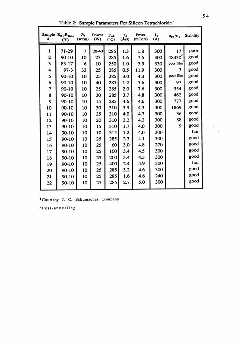
8/8/2019 An Electron-cyclotron-resonance Plasma Apparatus For
http://slidepdf.com/reader/full/an-electron-cyclotron-resonance-plasma-apparatus-for 62/79
5 4
Table 2: Sample Parameters For Silicon Tetrachloride
Sample RH2:Rsia4
^ ( % )
1
2
3
4
5
6
7
89
10
11
12
13
14
15
1617
18
19
20
21
22
71-29
90-10
83-17
97-3
90-10
90-10
90-10
90-1090-10
90-10
90-10
90-10
90-10
90-10
90-10
90-1090-10
90-10
90-10
90-10
90-10
90-10
1 Courtesy J. C. !
2post-a nnea l ing
0T(seem)
7
10
6
33
10
10
10
1010
10
10
10
10
10
10
1010
10
10
10
10
10
Schuma
Power T«A(W) (^C)
20-40
25
10
25
25
40
25
3015
30
25
20
15
10
25
2525
25
25
25
25
25
285
285
250
285
285
285
285
285285
310
310
310
310
315
285
60100
200
400
285
285
285
cher Companj
(A/s)
1.3
1.6
1.0
0.5
3.0
1.2
2.0
3.74.6
3.9
4.0
2.2
1.7
1.2
2.3
3.03.4
3.4
2.4
3.2
1.6
2.7
f
Press.(mTorr)
1.8
7.6
3.5
11.9
4.3
7.6
7.6
4.84.6
4.3
4.7
4.2
4.0
4.0
4.1
4.84.5
4.3
4.9
4.6
4.6
5.0
IB
(A)
300
300
330
300
300
300
300
300300
300
300
300
300
300
300
270300
300
300
300
240
300
CTph /c J Stability
17
48330'poor film
7poor film
97
354
462111
1869
36
88
9
poor
good
good
good
good
good
good
goodgood
good
good
good
good
fair
good
goodgood
good
fair
good
good
good

8/8/2019 An Electron-cyclotron-resonance Plasma Apparatus For
http://slidepdf.com/reader/full/an-electron-cyclotron-resonance-plasma-apparatus-for 63/79
5 5
ann ealin g, produ ced a cond uctivity ratio of 48,3 3 0. This opto
electronic property is comparable to good quality glow discharge
a-Si:H films. Th e anne aling process relaxe s the film structure and
improves the si l icon-hydrogen bonding, thereby reducing the
den sity of state s. The cond uctivity ratio prior to annealing was
found to be 140.
Because sample 2 showed a high photoconduct ivi ty, the
relative flow rate for SiCU of 10% was used for all remaining
samples produced. The microwave power was the next parameter
varied for samples 5 through 9. The substrate temp erature (Tsub)
was increased from 285 °C to 310 °C for the next five samples (10
thru 14), with the microwave power again being the parameter
va ried . A second SiCU gas source was used for sam ples 15
through 22 since the first source was suspected of being
co ntam inate d with oxy gen . For samp les 15 through 19 the
substrate temperature was varied from no substrate heating to
400 °C in incre ments of 100 °C. Sam ples 15 and 20 through 22
were produced to investigate the reproducibility of the process.
It is important to note that the deposition rates for the six
samples made under identical conditions (sample's 2,5,7,15,20,and
22) w ere not very consiste nt with each other. It is believed thatthis is caused from film buildup on the chamber walls as the
ove rall proc essin g time incre ase s. The film previous ly deposited
on the walls becomes partially etched during the deposition
proc ess, and contributes to the deposition proce ss. Observations

8/8/2019 An Electron-cyclotron-resonance Plasma Apparatus For
http://slidepdf.com/reader/full/an-electron-cyclotron-resonance-plasma-apparatus-for 64/79
5 6
have shown that the deposition rates increase for later runs at the
same operat ing condit ions.
The operating parameters, deposition rates, and conductivity
ratios for the samples produced from a proprietary liquid source,
courtesy of the J. C. Schumacher company, and hydrogen gas are
tabulated in Tab le 3 . All samples produced from this gas source
contained a very large amount of carbon which produced poor
qua lity films . Th ese carbon alloyed am orphous silicon films (a-
SiC:H) could possibly be used as a window layer (wide bandgap
m ateria l) in p-i-n type solar cells . The first two samples were the
initial sam ples produ ced in the ECR deposition appa ratus. They
were produced prior to the installation of the circulator and
dummy load; at a t ime when the plasma discharge conditions
we re very poo r. The poor discharge condition was believed to be
caused by unstable magnetron operat ion at the low appl ied
pow ers. The rem aining seven liquid source (L.S.) samples were
produced after the circulator and dummy load were installed, at
which t ime the discharge process improved rem arkably. The
relative flow rates for the liquid source ( R L . S . ) gas and hydrogen
( R H 2 ) g^s were varied so as to investigate the percent carbon
co nte nt in eac h film . The total gas flow rate and substratetem pe ra tu re (Tsub) were held at their respective values for the
seven sam ples. The appl ied pow er, operat ing press ure, and
magnet coil current also stayed relatively constant as shown in
Ta ble 3 . From the table, the depo sition rates (rd) rem ain ed
rela t ive ly co nsta nt for samples 3 through 9, al though the
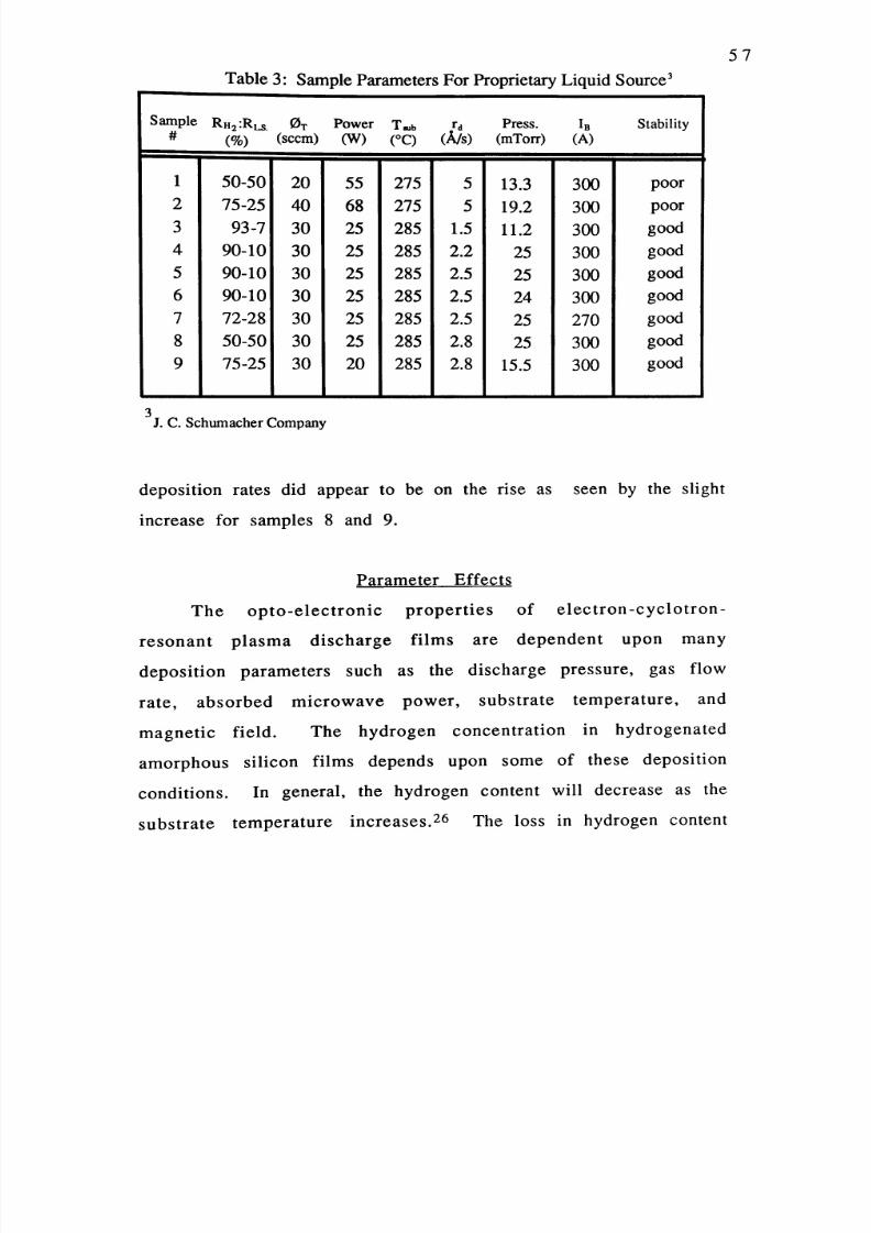
8/8/2019 An Electron-cyclotron-resonance Plasma Apparatus For
http://slidepdf.com/reader/full/an-electron-cyclotron-resonance-plasma-apparatus-for 65/79
5 7
Table 3 : Sample Parameters For Proprietary Liquid Source-
Sample#
1
2
3
4
5
6
7
8
'
R H 2 : R L 5 .
(% )
50-50
75-25
93-7
90-10
90-10
90-10
72-28
50-5075-25
0T(seem)
20
40
30
30
30
30
30
3030
Power(W )
55
68
25
25
25
25
25
2520
Tgub
275
275
285
285
285
285
285
285285
(A/s)
5
5
1.5
2.2
2.5
2.5
2.5
2.82.8
Press.(mTorr)
13.3
19.2
11.2
25
25
24
25
2515.5
IB
(A)
300
300
300
300
300
300
270
300300
Stability
poor
poor
good
good
good
good
good
good
good
J. C. Schumacher Company
dep osition ra tes did appear to be on the rise as seen by the slight
increase for samples 8 and 9.
Parameter Effects
Th e o p t o - e l ec t r o n i c p r o p e r t i e s o f e l ec t r o n - cy c l o t r o n -
resonant p lasma discharge f i lms are dependent upon many
deposition parameters such as the discharge pressure, gas flow
r a te , absorbed microwave power , subst rate temperature , and
m agn et ic f ield. The hydrogen conc entrat ion in hydrogenated
amorphous sil icon films depends upon some of these deposition
co nd ition s. In gene ral, the hydrogen content will decrea se as the
su bs trate tem pe ratu re increases.26 The loss in hydrogen content

8/8/2019 An Electron-cyclotron-resonance Plasma Apparatus For
http://slidepdf.com/reader/full/an-electron-cyclotron-resonance-plasma-apparatus-for 66/79
5 8
as the substrate temperature increases causes the densi ty of
defect states to increase.27
Film s d epos ited at low substrate tem peratures (< 200 °C) do
not exibit good elctronic prop erties. These films contain dihydride
(SiH2) and trihydride (SiHs) chains which act as recombination
cen ters. Ab ove 200 °C the hydrogen exists in mono hydride (SiH)
form. It is this fundam ental chang e to m onoh ydride bonding at
higher substrate temperatures that has a major effect on the
reduction of the density of states and, therefore, an improvement
in the opto-e lectronic properties of the ma terial . When a-Si:H
films are heated to temperatures greater than «350 °C, the
hydrogen evolves from the material , and the density of states
increases, causing a reduction in the opto-electronic properties.
Hydrogen content will also increase with an increase in applied
power, and decreases with an increase in discharge pressure.
In the following discussion the deposition rate is graphically
displaye d as a function of the various processing param eters. In
Figure 13 the deposition rate is plotted as a function of the
magnet coil current at various absorbed microwave powers (Pabs)-
For an absorbed power of 8 watts, the deposition rate does not
seem to be affected by an increase in the magnetic field, as long asit is above the threshold value ( I B = 1 8 0 A, B M « 0 . 0 6 3 T ) . It is not
until the applied power is further increased that an increase in
the magnetic field begins to affect the deposition rate, the rate
then displays a peak.

8/8/2019 An Electron-cyclotron-resonance Plasma Apparatus For
http://slidepdf.com/reader/full/an-electron-cyclotron-resonance-plasma-apparatus-for 67/79
5 9
TH ( A / S )
2 •
1 -
0
360
IrfA)
« Pabs=8W
• Pabs=10W
° Pabs=15W
A Pabs=50W
Figure 1 3. Deposition rate as a function of magnet coilcurrent at 0 T = 6 SCCM, P=2.6 mTorr, and RsiCU-
For the present ECR apparatus setup, a layer of enhanced
brightness always forms outs ide the magnet ic mirror
configuration (between the second magnet coil set and the
viewport, see Figure 9). We take this to be an ECR layer. At lowmagnetic field settings the ECR layer takes the shape of a thin disc
that cov ers the cross section of the discharge chamber. When the
magnetic field is increased, the ECR disc layer propagates towards
the sample holder, following the 0.0875 Tesla magnitude of the
flux density, and gradually forms into a donut-like shape touching

8/8/2019 An Electron-cyclotron-resonance Plasma Apparatus For
http://slidepdf.com/reader/full/an-electron-cyclotron-resonance-plasma-apparatus-for 68/79
6 0
the cha m ber wa ll. This change in the ECR layer probably changes
the makeup of the particle flux incident on the substrate and thus
the film dep osition rate. The ma ximu m seen in the depo sition-
rate curves may be due to high energy particles being slowed by
the cha m ber wall . A slowing of the part icles al lows more
dep osi t ion than etching to occur. Ad dit ional ly, the general
increase in deposition rate with absorbed power seen in Figure 13
is probably due to an increase in the ion density caused by the
higher power.
Figures 14 and 15 show the deposition rate plotted versus
the discharge pressure, at various absorbed powers, for total flow
rates ( 0 T ) of 10 SCCM and 33 SCCM, respectively. The relative
flow rate for the SiCU gas is 10% and the magnet coil current is
30 0 A m ps. Th ese two graphs show that the deposition rate, at
f ixed ab sorb ed pow er, is relat ive ly con stan t for different
disch arge pres sure s. The increase in the deposition rate, at a
constant pressure, for higher absorbed power is probably due to a
more efficient discharge produced by a greater ion density.
Figures 16 and 17 illustrate the deposition rate versus the
S iC U relative flow rate (R siC u) at various absorbed powers. Figure
16 is for a total flow rate of 10 SCCM at a discharge pressure of4.7 mTo rr, and a magnet coil current of 30 0 Am ps. From the plots
of Figure 16, for fixed absorbed power, it is easily seen that the
deposition rate increases to a maximum with increasing percent
S iC U gas in the discharge. The maximum deposition rates occur
ap pr ox im ate ly at 50 % SiCU relative flow rate for the higher

8/8/2019 An Electron-cyclotron-resonance Plasma Apparatus For
http://slidepdf.com/reader/full/an-electron-cyclotron-resonance-plasma-apparatus-for 69/79
6 1
r^CA/s)
30 40P (mTorr)
Pabs=5W
Pabs=10W
Pabs=15W
- Pabs=20W
A Pabs=25W
o
•
•
Fig ure 14. Deposition rate as a function of plasma discharge
pressure at 0 T = 1 O SCCM, I B = 3 0 0 A, and RsiCl4= 10^^-
appl ied pow ers. For conce ntrat ions of SiCU above 50% the
dep osi t ion rate gradu al ly drops unt i l etching occ urs. This
phenomenon is probably due to the increased number of chlorine
ions in the plasma discharge.
Figure 17 is for a total SiCU gas flow rate of 30 SCCM at a
disch arge pressu re of 11.4 mT orr. The curves for the deposition
rate follow a similar pattern as that discussed for Figure 16;
except that the deposition rates for relative flow rates beyond
50% are not shown since the maximum lies at 30%.

8/8/2019 An Electron-cyclotron-resonance Plasma Apparatus For
http://slidepdf.com/reader/full/an-electron-cyclotron-resonance-plasma-apparatus-for 70/79
^Akls)6 2
8
6 -
4 -
2 -
0
o Pabs=5W
• Pabs = 10W
° Pabs=15W
A Pabs=20W
A Pabs=25W
Fig ure 15. Deposition rate as a function of plasma discharge
pressure at 0 T = 3 3 SCCM, I B = 3 0 0 A, and RsiCl4= 10%-
ECR Apparatus Improvements
There are a number of different areas in which possible
additions and changes to the apparatus can be, and already have
been, made in an attempt to improve the discharge process; and
ultim ately to obtain better quality a-Si:H films. Relatively high
levels of metallic contaminants have been found in ECR deposited
samples which originate from the part of the stainless steel
chamber exposed to the high density ECR plasma discharge.28 It

8/8/2019 An Electron-cyclotron-resonance Plasma Apparatus For
http://slidepdf.com/reader/full/an-electron-cyclotron-resonance-plasma-apparatus-for 71/79
6 3
r^CA/s)
100
Rsicif'')
• Pabs =
n P .Ko=
» Pabs=5W'abs=10W
" ''abs=15W
A Pabs=20W
A Pabs=25W
• Pabs=30W
• Pabs =35 W
• Pabs=40W
Figure 16. Deposition rate as a function of SiCl4 relative flowrate at 0 T = 1 O SCCM, I B = 3 0 0 A, and P=4.7 mTorr.
was found that these metallic impurity levels can be greatly
reduced by covering the stainless steel chamber wall at the ECR
layer with an anodized aluminum sleeve. W e have had a number
of anodized aluminum sleeves fabricated, and these are ready for
future thin film produ ction. Confinement of the ECR discharge
between the magnetic-mirror producing coil sets can be
accomplished by placing a stainless steel screen to the right of the
second magnet co il set (see Figure 9). This wi ll prevent the
microwaves from propagating beyond the magnet coil and setting

8/8/2019 An Electron-cyclotron-resonance Plasma Apparatus For
http://slidepdf.com/reader/full/an-electron-cyclotron-resonance-plasma-apparatus-for 72/79
6 4
r.CA/s)
12
8 -
4 -
0
o
•
D
•
A
^ S i C l f )
Pabs =5 W
Pabs=10W
Pabs=15W
Pabs=20W
Pabs=25W
Pabs=30W
Pabs=35W
Pabs=40W
Figu re 17. Deposition rate as function of SiCU relative flowrate at 0 T = 3 O SCCM, I B = 3 0 0 A, and P=11.4 mTorr.
up a d isch arge beyond the ma gnet ic-mirror sect ion . The
acquisition and installation of a stainless-steel screen is currently
being performed for future a-Si:H film production, and to
investigate its effects upon film deposition.
Another poss ib le improvement involves redesigning the
sam ple plug (see Figu re 11(b)). The crystalline silicon and glass
sub strate s are held in plac e by four sma ll screw s. From visual
inspection of the deposited films, it is apparent that the screws
affect the film dep osition near their loca tion. Co nce rning the

8/8/2019 An Electron-cyclotron-resonance Plasma Apparatus For
http://slidepdf.com/reader/full/an-electron-cyclotron-resonance-plasma-apparatus-for 73/79
6 5
sample feedrod, during sample insertion slight leakage can be
obse rved from the cham ber pressu re reado ut. The leakage occurs
at the sing le 0- rin g that seals the feedrod. Although vacuum
grease and 0-ring replacement minimizes this problem, a different
type of feedrod seal is sugg ested. The addition of a hinged load-
lock door for sample insertion and retrieval is another possible
improvement; current ly, much t ime is wasted removing and
replacin g m any bolts. For the liquid source gas flow rate, a more
sensi t ive mass f low control ler is necessary to improve the
repe atab ility of the flow setting. This improvem ent has just been
accomplished by reducing the range of the mass flow controller
redu ced . A new temperture controller is being fabricated in order
to obtain improved constant substrate temperatures, and also to
extend the heating element lifetime.
The most important improvement needed is to replace the
silicon tetrac hlorid e gas source with silane (SiH4) gas. This will
el iminate the chlorine from the discharge, and produce pure
hydro gena ted amo rphous sil icon films. W ork is presently being
do ne to accom plish this task. Safety precaution s have to be taken
into account when converting over to silane due to the explosive
nature of the gas. Acc om plishing this changeover will give TexasTech University the distinction of having the only microwave ECR
plasma apparatus producing a-Si:H films in the country.
A new toroidal ECR deposition system is in the final
con struc tion s tage . Th e new system will perform the same task as
that of the ECR depos ition system discussed earlier. The magnetic

8/8/2019 An Electron-cyclotron-resonance Plasma Apparatus For
http://slidepdf.com/reader/full/an-electron-cyclotron-resonance-plasma-apparatus-for 74/79
6 6
field is obtained from electrically insulated, water-cooled, copper
tubing wrapp ed around the exterior of the toriodal cham ber. This
new toroidal chamber will replace the deposition chamber and
m ag net coi l sets shown in Figure 9. How ever, al l other
subsystems will remain the same.
Conclusion
This microwave ECR plasma deposition plasma apparatus has the
abi l i ty to operate with different source gases, f low rates,
microwave powers, magnetic field strengths, operating pressures,
and sam ple tem pera tures and voltag es. The system has also
shown the ability to produce stable, repeatable, and controllable
plasm a discharges for a wide range of processing param eters. The
microwave ECR plasma deposition apparatus has shown promising
results in producing a-Si:H,Cl films that are comparable to a-Si:H,Cl
films prod uce d by the glow discha rge proc ess. W ith the added
improvements mentioned above, and the eventual changeover to
silane gas, the ECR apparatus will be in a position to produce high
quality a-Si:H films.

8/8/2019 An Electron-cyclotron-resonance Plasma Apparatus For
http://slidepdf.com/reader/full/an-electron-cyclotron-resonance-plasma-apparatus-for 75/79
REFERENCES
1. J. P. M. Schmitt, Thin Solid Films, vol. 174, p. 193, 1989.
2. D. E. Carlson, C. R. Wronski, ADDI. Phvs. Lett., vol. 28, p. 671,1 9 7 6 .
3 . D. E. Carlson, "Semiconductor device having a body of
amorphous sil icon," U.S. Patent 4 064 521, 1977.
4 . A. Madan, M. P. Shaw, "The Physics and Applications of
Amorphous Semiconductors," p. 162, Academic Press, Inc.,
San Diego, CA, 1988.
5 . D. E. Carlson, IEEE Tran. Elec. Dev.. vol. 36, p. 2775,1989.
6. T. Kagawa, N. Matsumoto, K. Kumada, Jpn. J. Appl. Phvs.. vol.
2 1 , p. 251, 1982.
7 . P. G. Lecomber, W. E. Spear, A. Gaith, Electron. Letter, vol. 15, p.
179, 1979.
8. A. Catalano, Proc. 19th IEEE Photovoltaic Specialists Conf..
p .1506 , 1987.
9. J. Yang, Proc. 19th IEEE Photovoltaic Specialists Conf.. p. 241,
1 9 8 8 .
10 . D. L. Morel, Proc. 8th E. C. Photovoltaic Solar Energy Conf.. p. 661,
1 9 8 8 .
1 1 . D. E. Carlson, IEEE Tran. Elec. Dev.. vol. ED-24, p. 449,1977.
12. J. Kane, "Photodetector with enhanced light absorption," U. S.
P a t e n t 4 532 537, 1985.
1 3 . C. R. Wronski, Solid State Tech.. vol. 46, p. 114, 1988.
14 . A. Madan, M. P. Shaw, "The Physics and Applications of
Amorphous Semiconductors," p. 168, Academic Press, Inc.,
San Diego, CA, 1988.
6 7

8/8/2019 An Electron-cyclotron-resonance Plasma Apparatus For
http://slidepdf.com/reader/full/an-electron-cyclotron-resonance-plasma-apparatus-for 76/79
6 8
15 . D. L. Staebler, C. R. Wronski, Appl. Phvs. Lett., vol. 31, p. 292,1 9 7 7 .
16 . M. Stutzman, W. B. Jackson, C. C. Tsai, Phvs. Rev., vol. B32, p.
22. 1985.
17. H. Ohagi, M. Yamazaki, J. Nakata, J. Shirafuji, K. Fujibayashi, Y.Inuishi, Tech. Digest PVSEC-3. Tokyo, 1987, p. 671, 1987.
18. H. Ohagi, M. Yamazaki, J. Nakata, S. Imao, J. Shirafuji, K.Fujibayashi, Y. Inuishi, Jpn. J. Appl. Phvs.. vol. 27, p. L916,1 9 8 8 .
19. W. B. Ard, M. C. Becker, R. A. Dandl, H. O. Eason, A. C. England,J. R. Kerr, Phvs. Rev. Lett., vol. 10, p. 89, 1963.
2 0 . D. B. Miller, G. W. Bethke, AIAA J., vol. 4, p. 835, 1966.
2 1 . Y. Imai, K. Ohwada, J. Vac. Sci. Technol. B. vol. 5, p. 889, 1987.
2 2 . T. Ono, C. Takahashi, S. Matsuo, Jpn. J. Appl. Phvs.. vol. 23, p.L534, 1984.
2 3 . N. Sakudo, T. Tokiguchi, H. Koike, I. Kanomata, Rev. Sci. Instrum..vol. 54, p. 681, 1983.
2 4 . H. Karawada, K. S. Mar, A. Hiraki, Jpn. J. Appl. Phvs.. vol. 26, p.L1032, 1987.
2 5 . J. Asmussen, J. Vac. Sci. Technol.. vol. A7, p. 883, 1989.
2 6 . A. Madan, P. LeComber, W. Spear, J. Non Crvst. Solids, vol. 20, p.
239, 1976.
2 7 . P. J. Zanzucchi, C. R. Wronski, D. E. Carlson, J. Appl. Phys., vol. 48,p. 5227, 1977.
2 8 . A. S. Yapsir, G. Fortuno-Wiltshire, J. P. Gambino, R. H. Kastl, C. C.Parks, T Vac. Sci. Technol.. vol. A8, p. 2939, 1990.

8/8/2019 An Electron-cyclotron-resonance Plasma Apparatus For
http://slidepdf.com/reader/full/an-electron-cyclotron-resonance-plasma-apparatus-for 77/79
P E R M I S S I O N T O C O P Y
In p r e s e n t i n g t h i s t h e s i s I n p a r t i a l f u l f i l l m e nt o f th e
r e q u i r e m e n t s f or a m a s t e r ' s d e g r e e a t T e x a s T e c h U n i v e r s i t y , I a g r e e
t h at t h e L i b r a r y a n d m y o iajor d e p a r t m e n t s h a l l m ake it f r e e l y a v a i l
a b l e f o r r e s e a r c h p u r p o s e s . P e r m i s s i o n t o c o p y th i s t h e s i s f or
s c h o l a r l y p u r p o s e s m a y b e g r a n t e d b y t h e D i r e c t o r o f t h e L i b r a r y or
m y m a j o r p r o f e s s o r . It i s u n d e r s t o o d t ha t a n y c o p y i n g o r p u b l i c a t i o n
o f t h i s t h e s i s f or f i n a n c i a l g a i n s h a l l n o t b e a l l o we d wi t h o u t m y
f u r t h e r wr i t t e n p e r m i s s i o n a n d t ha t a n y u s e r m ay b e l i a b l e f o r c o p y
r i g h t i n f r i n g e m e n t .
D i s a g r e e ( P e r m i ss i o n n o t g r a n t e d ) A g r e e ( P e i m i s si o n g r a n t e d )
S t u d e n t 's s i g n a t u r e S t u d e n
///z^/?^D a t e D a t e

8/8/2019 An Electron-cyclotron-resonance Plasma Apparatus For
http://slidepdf.com/reader/full/an-electron-cyclotron-resonance-plasma-apparatus-for 78/79
o

8/8/2019 An Electron-cyclotron-resonance Plasma Apparatus For
http://slidepdf.com/reader/full/an-electron-cyclotron-resonance-plasma-apparatus-for 79/79