Embed Size (px)
Citation preview

AN EBD APPROACH TO EMBEDDED PRODUCT DESIGN
Jun Zhang
A Thesis
in
The Department
of
Concordia Institute for Information Systems Engineering
Presented in Partial Fulfillment of the Requirements
for the Degree of Master of Applied Science (Quality System Engineering) at
Concordia University
Montreal, Quebec, Canada
Quality Systems Engineering
November 2011
© Jun Zhang, 2011

ii

iii
ABSTRACT
AN EBD APPROACH TO EMBEDDED PRODUCT DESIGN
Jun Zhang
In contrast to general-purpose computers, an embedded system has a special function for
a special purpose. Nowadays, embedded products play an important role in daily life, and
they are widely used almost everywhere, such as in GPS, mobile phones, digital TV,
transportation systems, computer systems in aircraft, computer systems in vehicles.
Despite its popularity, the development process for embedded products is usually very
complicated and thus very often results in over time (development time), or in over-
budget (cost) or a lack of expected product specifications. Therefore, it is necessary to
use an appropriate prescriptive method or design methodology to guide a designer in the
design process.
The objective of the present thesis is to introduce a new approach to embedded system
engineering to implement a new embedded product design. A rich working experience in
industry suggests that there is a need for such work. Compared to the traditional
approach, which uses product-based or process-based design analysis, the proposed
approach uses environment-based design (EBD) methodology for the whole embedded
system development life cycle, which may be a systematic procedure aimed to help
designers during embedded product development. To better illustrate the application of
the proposed design approach to embedded system engineering, an original example of
an embedded ARM Linux system is used as a case study in the present thesis.

iv
ACKNOWLEDGMENTS
I would like to thank Professor Yong Zeng for constructive and insightful suggestions
and guidance during my graduate career in his Design Lab. I thank him for helpful
suggestions and his constant encouragement.
I want to thank all the members in the Design Lab, especially Suo Tan and Thanh An
Nguyen.
Finally, I also take this opportunity to thank my family. Without their support, I would
not have gone so far.

v
Table of Contents
List of Figures .................................................................................................................. viii
List of Tables .......................................................................................................................x
Chapter 1 INTRODUCTION ...............................................................................................1
1.1 Background ................................................................................................................1
1.2 Copyright statement about case studies .....................................................................2
1.3 Motivation ..................................................................................................................3
1.4 Contributions ..............................................................................................................4
1.5 Thesis organization ....................................................................................................5
Chapter 2 EMBEDDED SYSTEM DESIGN ......................................................................7
2.1 Embedded systems .....................................................................................................7
2.1.1 Introduction of embedded Linux system: terminology ...................................... 8
2.1.2 Embedded product structure ............................................................................. 13
2.1.3 Embedded system design flow ......................................................................... 14
2.1.4 Recommendation of a good design in an embedded product design ............... 16
2.2 Criteria of an effective design methodology ............................................................16
2.3 Embedded system design methodology: related work .............................................17
2.4 Motivation of the EBD in embedded system design ................................................23
Chapter 3 APPLICATION OF EBD TO EMBEDDED PRODUCT DESIGN ................24
3.1 Case study introduction ............................................................................................25

vi
3.2 Overview: why EBD in an embedded system development ....................................26
3.3 Understanding design problems: embedded product life cycle environment analysis30
3.4 Analyzing design problems: conflict identification in embedded product life cycle43
3.5 Solving design problems: solution generation .........................................................48
Chapter 4 VALIDATION OF EBD: EMBEDDED PRODUCT DEVELOPMENT - A
CASE STUDY ...................................................................................................................50
4.1 Introduction ..............................................................................................................51
4.1.1 Additional case review ..................................................................................... 51
4.1.2 Must-do task list for a detailed product development ...................................... 53
4.1.3 Example of a hidden problem ........................................................................... 55
4.2 Development process without EBD methodology ...................................................56
4.2.1 Product development process ........................................................................... 56
4.2.2 Quality of development process ....................................................................... 64
4.3 Analyzing and diagnosing the development process using EBD ............................65
4.3.1 Adjustment of the development process using EBD ........................................ 65
4.3.2 Design state....................................................................................................... 75
4.3.3 Distrusted variables life time ............................................................................ 93
4.3.4 EBD approach to the development process: examples ..................................... 95
4.3.5 Result of EBD approach ................................................................................... 96
4.4 Quality of two approaches........................................................................................97
vii
Chapter 5 CONCLUSIONS AND FUTURE WORK ......................................................98
5.1 Conclusion: why use an EBD in embedded system design .....................................98
5.2 Future work ............................................................................................................100
APPENDIX ......................................................................................................................101
1.1 Overview of environment-based design .................................................................101
1.2 Recursive object model ..........................................................................................101
1.2.1 Mathematical foundation ................................................................................ 102
1.2.2 ROM: graphical representation of natural language ....................................... 103
1.2.3 ROMA: translation of natural language to ROM diagram ............................. 105
1.3 Formulization of design requirements....................................................................106
1.4 Environment analysis .............................................................................................109
1.5 Conflict identification ............................................................................................112
1.6 Solution generation ................................................................................................113
1.7 Relationships between the three activities of EBD ................................................114
Bibliography ....................................................................................................................115

viii
List of Figures
Figure 1 Embedded system schematic example: memory interface .................................. 9
Figure 2 An embedded system PCB example.................................................................. 10
Figure 3 Crossing development environment - An example: a distributed system
development ...................................................................................................................... 12
Figure 4 An example of an embedded system ................................................................. 13
Figure 5 Scope of the development/design in the present thesis ...................................... 15
Figure 6 The system ......................................................................................................... 25
Figure 7 Three major product environments [36] ............................................................. 27
Figure 8 Seven events & eight levels for design requirements [37] ................................. 28
Figure 9 EBD process model [36] .................................................................................... 28
Figure 10 Illustration of problems existing in software product development [38] ......... 29
Figure 11 Created first ROM diagram .............................................................................. 32
Figure 12 Created first updated ROM diagram ................................................................ 33
Figure 13 Seven events & eight levels of requirements-AB[19] ...................................... 38
Figure 14 Conflict relationships analysis: an example ..................................................... 47
Figure 15 The best roadmap for solving the conflicts ..................................................... 49
Figure 16 The remote station system components ........................................................... 53
Figure 17 An example of SDRAM mounting – hidden problems ................................... 55
Figure 18 An example of results from SDRAM pins problems- effect from a hidden
problem ............................................................................................................................. 56
Figure 19 Detailed development process without using EBD ......................................... 63

ix
Figure 20 Detailed development process with EBD application ..................................... 74
Figure 21 Design state & development time.................................................................... 75
Figure 22 Variables in each design environment & development time ............................ 93
Figure 23 EBD approach to the development process ...................................................... 95
Figure 24 Quality of two approaches ................................................................................ 97
x
List of Tables
Table 1 Rules for generic questions[39] ........................................................................... 34
Table 2 Generic domain questions and answers ............................................................... 35
Table 3 Specific domain questions and answers example using ROM ............................ 38
Table 4 Lifecycle analysis of the embedded product design problem- specific domain
questions ........................................................................................................................... 42
Table 5 Conflict identification .......................................................................................... 44
Table 6 Root conflicts analysis ......................................................................................... 48
Table 7 Technical to-do list for the development ............................................................. 54
Table 8 Detailed system development process and its duration ....................................... 57
Table 9 Result without EBD ............................................................................................. 64
Table 10 EBD analysis for phase one .............................................................................. 66
Table 11 EBD diagnose for phase two ........................................................................... 69
Table 12 EBD analysis and diagnose for phase three ...................................................... 72
Table 13 X variable & C constant: two examples ............................................................ 94
Table 14 Result with EBD ................................................................................................ 96

1
Chapter 1
INTRODUCTION
1.1 Background
In contrast to general-purpose computers which are designed to meet the needs of many
different end-users, an embedded system has a special function for special purpose [1].
In other words, an embedded system is designed to perform a special function. The
earlier development of modern embedded systems can be dated back to the 1960’s.
Apollo Guidance Computer, developed at the MIT Instrumentation Laboratory in the
1960’s, is one of the early recognizably modern embedded systems. Since then,
embedded systems have gone through a dramatic evolution. The price of embedded
systems has significantly decreased whereas the processing power and functionality has
dramatically increased. This leads to the significantly increased popularity of embedded
systems in a wide range of devices.
In the past half century, embedded systems have undergone a dramatic evolution which
has resulted in a significantly decreased cost and increased functionality. This, in turn,
leads to the greatly increased demand for embedded products. Nowadays, embedded
products play an important role in everyday life and are widely used in daily life, such as
global positioning systems (GPS), mobile phones, digital television (TV), transportation
2
systems, computer systems in aircraft, and computer systems in vehicles. The
development process for embedded products is very complicated and thus fails very
often. Therefore, it is important to use an appropriate design methodology to control
design quality. For example, the author has found that some embedded system
development projects fail without even starting to write a single code due to a
misunderstanding of design requirements. Therefore, it is important to use an appropriate
design methodology to assist the design process and to control design quality.
The present thesis illustrates how to apply EBD to embedded product designs.
1.2 Copyright statement about case studies
The author of the present thesis has worked on the design of embedded systems in
different scales. Due to the copyright from the confidential agreement that the author
has signed with different organizations, the author has no written permit from a company
to use real projects as the case study and therefore those industrial case studies cannot be
used in the present thesis. Instead, the author created the original case study for the
present thesis research.
This is to state that the case study is not associated with any real industrial project or
company. In regard to the case study, two things can be stated with confidence because
3
of the author’s rich working experience in industry:
For the purposes of showing EBD approach to embedded system design, there is
no difference between the embedded system example used here and that of a real
project used in a company;
The example chosen is comparable to a project from the real world.
Consequently, this thesis does not break any confidential agreement that the
author has signed with any organization.
1.3 Motivation
Many IT companies do not have final sellable products even if they have great ideas in
the beginning. In order to have sellable products to release and to allow entry into the
market as soon as possible, designers often suffer some kind of stress due to budget, the
expected development duration of the product, and product quality requirement. These
conditions may affect the designers’ creation during the process of developing new
products. It is very common for expert designers to appear to be “ill-behaved” problem
solvers, especially in terms of the development duration and product cost. Therefore, it is
very important to develop a new design methodology that can help designers in the
process of product design and lead to the improvement of design efficiency, as well as
product quality.

4
The objective of the present thesis is to show how to apply EBD to embedded product
development to improve design quality. It is hoped that by applying EBD to embedded
product development, product quality will be improved and that many IT companies will
benefit. In other words, the results of the proposed research will satisfy the needs of
many IT companies, particularly those of companies that have to develop more
competitive products and take some market share away from their competitors.
1.4 Contributions
In the present thesis, the description of EBD is attached in the appendix. In the present
thesis, a brief review of embedded systems is first given, as well as the design
methodology for embedded system development. This is followed by the illustration of
how to apply EBD to embedded system development. In addition, the validation of EBD
will be discussed. The main contributions of this thesis include the following:
(1) A new approach to embedded system design, conceptual design model EBD, is
proposed to guide embedded developers in the design process. This is a new model
in embedded system engineering.
The first stage of EBD (environment analysis) benefits both managers in
development engineering and developers. The second stage of EBD (conflict
5
identification) and the third stage of EBD (solution generation) are beneficial mainly
to developers. However, that concept also works for managers.
(2) The application of EBD to an embedded product design is illustrated by the general
concept.
(3) To illustrate the application of the proposed model and the quantitative approach,
the case of an embedded ARM Linux product, a real-world example, is adopted
studied as a case study.
1.5 Thesis organization
The rest of the present thesis is organized as follows:
(1) Chapter 1 INTRODUCTION: introduction of the background, motivation and
contributions;
(2) Chapter 2 EMBEDDED PRODUCT DESIGN: introduction of the embedded system
terminology, the embedded product structure, the embedded system design flow, and
the recommendation of a good design in an embedded product design;
(3) Chapter 3 APPLICATION OF EBD TO EMBEDDED PRODUCT DESIGN:
explanation of why EBD can be used to embedded system development, and from
general point of view, explanation of how to apply EBD to an embedded product
design step by step: understanding design problems, analyzing design problems, and
then solving design problems. An example (no confidential data from a real

6
company are used) is used to show how to apply the EBD for practiced application.
(4) Chapter 4 VALIDATION OF EBD: EMBEDDED DEVELOPMENT CASE
STUDY: review of the case including an additional introduction, and then
description of detailed development process. This is followed by the validation of the
result with two different design procedures – by using EBD and by not using EBD.
(5) Chapter 5 CONCLUSIONS AND FUTURE WORK: concluding remarks about why
an EBD in embedded system design and future work.
In the present thesis, the description of EBD is attached in the appendix. If you want to
know what EBD is , please go to Appendix.
7
Chapter 2
EMBEDDED SYSTEM DESIGN
In Chapter 1, the background of the embedded system design is introduced. Then some
basic terminology used in embedded systems is explained, and the recommendation of a
good embedded design is explained. Finally, in Chapter 4, EBD is validated whether or
not EBD design methodology can help an embedded designer to reach a high level of
embedded design.
The objective of the present thesis is to bring a new design methodology to embedded
product design engineering, thereby enhancing the quality of design. To achieve this
objective, this literature review covers the following areas:
(1) Introduction of the embedded system : terminology
(2) Embedded system design methodology: related work
2.1 Embedded systems
Embedded products are widely used in daily life, such as GPS, mobile phones, digital
TV, transportation systems, aircraft computer systems, vehicles. The development
process is complicated and thus fails very often.

8
It is difficult to define or to describe embedded systems precisely. There have been
many different definitions for embedded systems because the field is a wide and varied.
The following are some examples of possible definitions:
An embedded system is a special function for special purpose computer system
with a combination of hardware and software[1].
An embedded computer system (or simply an embedded system) is “a digital
system which uses a microprocessor running software to implement some or all
of its functions” [2].
For the different operating system (OS), we have the embedded Linux system, the
embedded Windows CE, embedded VXWORKS, the embedded android system and so
forth. According to the CPU, there are embedded ARM system, embedded PPC system,
embedded Intel system, etc.
2.1.1 Introduction of embedded Linux system: terminology
A brief overview of some terminologies used for embedded systems is given below:
(1) Embedded hardware (embedded HW):
a) Schematic( SCH ) : in an embedded system design, a schematic diagram is a diagram
showing the logic of the hardware – used for the product and also often reflects the pre-

9
design of the printed circuit board (PCB) [3].
An example of a SCH is shown in the following Figure 1:
Figure 1 Embedded system schematic example: memory interface
b) PCB: A printed circuit board (PCB) is designed for manufacturing or fixing a target
board. It mechanically supports Chips on the board. This kind of system is called a System
on Board (SOB). System on Chip (SOC) is not the topic in the thesis. In addition, a PCB
electrically connects electronic components through conductive pathways, VIAs, tracks or
signal traces. It is etched from copper sheets laminated onto a non-conductive substrate [4-
6].
An example of a PCB is shown below in the following Figure 2:

10
Figure 2 An embedded system PCB example
(2) Embedded software (embedded SW)
a) Boot loader
A CPU can only execute program code found from ROM or RAM. And operating systems
and applications images are stored on nonvolatile date storage such as NAND flash, NOR
flash or NFS server. When an embedded system is first powered on, it usually does not have
an operating system in ROM or RAM. The computer system has to execute a minimum image
from ROM. This image is the boot loader image [7].
The job of the Boot Loader is to initialize minimum hardware components from an unknown
state to a known state, to load the kernel from the loading memory to the running memory and

11
so on. Examples of boot loaders are the following: bootstrap loader, LILO, GRUB, ROLO,
Loadin, Etherboot, LinuxBIOS, Compaq’s bootldr, blob, PMON, sh-boot, u-boot, 2nd boot
loader. Multiple-stage boot loaders are used according to the platform. Their design constraints
are that they often need to have a small footprint due to one-time use.
b) Kernel
A kernel is a bridge between user applications and the hardware. The job of kernel is to
process date and to manage the system resources and the hardware system. The kernel is the
main part of computer operating systems [8].
c) Device driver
In an embedded system, usually, the hardware connects to the communications subsystem or
the computer bus. Therefore, device driver software is to allow the higher-level computer
programs to interact with a hardware device. For example, when a program calls up routines
in the device driver, then the driver sends commands to the hardware device. Applications
talk to hardware devices through the device driver [9].
d) Root file system
Applications would be able to access any data by file name or directory with a file system. A
file system's job is mainly to organize data, manage the available space on the device(s),
provide mechanisms to control access to the data and metadata, and update data in the same
file at nearly the same time. Some file systems, such as procfs, may be virtual distinguishable
12
from a directory service and registry[10].
e) Application
An application, often called “app”, helps the user to perform specific functions such as
calling on media players software , GUI functions , Microsoft Office , android applications
for education. Apps may be separated from the kernel in some operating systems such as
Linux. In some operating systems such as VXWORKS, they are not separated. The system
software serves the application in terms of user [11].
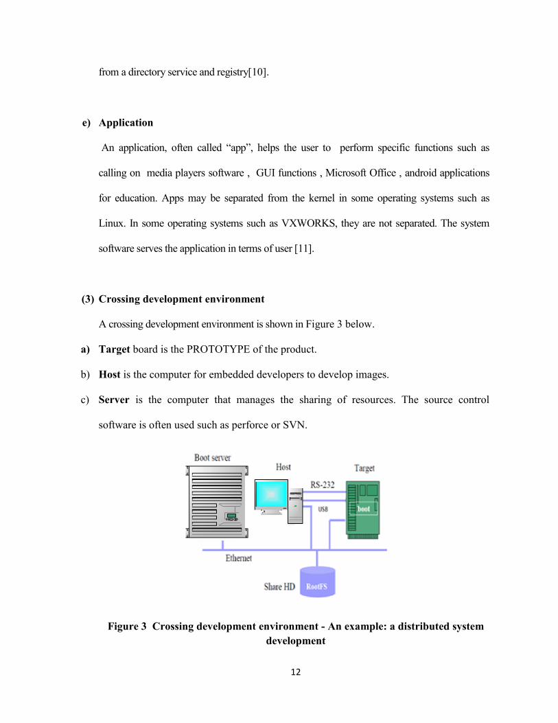
(3) Crossing development environment
A crossing development environment is shown in Figure 3 below.
a) Target board is the PROTOTYPE of the product.
b) Host is the computer for embedded developers to develop images.
c) Server is the computer that manages the sharing of resources. The source control
software is often used such as perforce or SVN.
Figure 3 Crossing development environment - An example: a distributed system
development

13
2.1.2 Embedded product structure
To sum up, in general, an embedded system structure may resemble the structure shown
in the following Figure 4:
Figure 4 An example of an embedded system
The peripherals of an embedded system may be different due to different product. For
example, the core of embedded systems talks with the outside world via peripherals.
Examples are the following: Serial Communication Interfaces (SCI), Multi Media Cards
(SD Cards, Compact Flash etc.),Networks( Ethernet, Lon Works, etc.), Discrete
IO(General Purpose Input/output ), Analog to Digital/Digital to Analog, Debugging(
JTAG, ISP, ICSP, BDM Port, BITP, and DP9 ports) , GPS. For example, if you are
developing a digital camera, you may have the following peripherals: LCD for display,
flash memory for storage, RAM for running images, a keyboard for the user to input, a
speaker to play sounds, a USB to connect to a printer or a PC.

14
If an embedded system is too simple, the loader, kernel, ROOTFS, drivers, applications
may be optional. SW may not have a kernel (operating system) such as the MCS-51
based embedded system used many years ago, or it may not need to develop drivers…
2.1.3 Embedded system design flow
A new embedded product life cycle may be different. The scope of the
development/design would therefore be different.
Figure 5 shows a general embedded product life cycle. The topic in the present thesis
would include only the development process shown in the rectangle with the red shape:
design requirements, design, debug/test, software-based electronic components test in a
manufacturing process, and redefined design requirements.

15
Figure 5 Scope of the development/design in the present thesis
This Figure 5 also shows an example of the development process in an embedded
product life cycle.

16
2.1.4 Recommendation of a good design in an embedded
product design
A recommendation for a good embedded product design/development would be as
follows:
Product features (final design) meet with most design requirements. In other words,
a good embedded product design should give customers satisfaction;
Development time is short ;
Cost is low ;
It is easy to update HW/SW; it is possible to update HW/SW; and the updating cost
is not too high.
A quality process in embedded product development should at least include points 1, 2,
and 3 given above. In industry, experienced engineers should pay more attention to the
4th point above.
2.2 Criteria of an effective design methodology
An effective design methodology should:
(1) Be able to help the designer have a “good design” in terms of shorter
development time and cost, as mentioned in the last section.
(2) Be able to guide a designer to jump out of a recursive loop[12]
(3) Be able to improve design process[13] [2].

17
2.3 Embedded system design methodology: related
work
The first conference on design methodology was held in London in 1962 [14] . Since
then, many conferences on this topic have been held due to the increased realization of
the importance of design methodology. In terms of the development of engineering
design methodology, there was significant improvement of it in the 1980s[15]. Although
many design methodologies have been proposed in this area so far, due to the complexity
of embedded systems, it is very hard to find one approach that fits all.
In this section, there is a brief review of some related existing major embedded system
design methodologies and their advantages and disadvantages. Some of the representative
major embedded system design methodologies are summarized as follows:
(1) The test-driven development of embedded systems
This method is based largely on test-driven development using existing software test
infrastructures (such as Extreme Programming) with both custom hardware and
custom software. They use Extreme Programming trying to detect the problems
caused by changing earlier requirements. For example, a developer first writes failing
test cases for the necessary functionality, and then writes code, debugs the system,
and then refractors as necessary until 100% of the test cases pass[16].

18
The advantage of this method is that it tries to detect problems earlier under changing
requirements. However, the main disadvantage of this method is that it uses existing
software to test infrastructures. Three questions must be asked:
Can the hardware be trusted in an embedded product design based on an
earlier process?
Can the software be trusted in an embedded product design based on an earlier
process?
Where is the existing trusted software in an embedded product design based
on an earlier process?
We cannot use a distrusted hardware or software to test other hardware or
software. We can use trusted hardware or software to test other hardware or
software.
(2) Platform-Based Design methodology for embedded systems
Platform-Based Design methodology reduces time-to-market in terms of development
time[17]. Examples are the TI OMAP platform for cellular phones, the Nexperia
platforms for consumer electronics, the Intel Centrino platform for laptops. However,
Business Week reported that Intel CEO Ottellini called those kind of companies are a
“platform company” [18]. Many companies approach platform development simply
as ABC(ad hoc, Bottom-up, and Core-centric) [17]. Alberto Sangiovanni-Vincentelli

19
and Grant Martin (the authors) believe that Platform-Based Design is “top-down”,
“Bottom-up” and “meet-in-the- middle” [19]. Alberto Sangiovanni-Vincentelli and
Grant Martin also believe that the embedded system design involves two essential
components: a rigorous methodology for embedded software development and
platform-based design[19]. Motorola’s Silver and Green Oak, “develop a family of
similar chips that differ in one or more components but are based on the same
microprocessor” [19]. Such a chip family is also a platform[19].
The advantage of this method is that the time-to-market may be shorter because of
using the platform. Also , because the system platforms may already be defined,
what the designers need to do is just apply it[20]. However, one of the biggest
disadvantages of this approach is that a platform gives the designer only limited
choices [21]. This is because a different products have different functions different
constraints. So, different architecture platforms may need to be applied. This is not
difficult to understand.
(3) Hardware/Software Co-design
Traditional embedded system design develops hardware and software separately[22].
Many researchers are trying to develop and improve this Co-design approach[22]
.This approach is to find out what the well-understood design problems are, and also
what the unsolved design problems are, as well as the relationship between hardware
and software in the early stages of embedded system design [23] , because SW and
HW shares resources in the embedded product [20].

20
However, to make a good design tradeoffs, the designer has to be knowledgeable in
both hardware and software domains [23].
In other words, hardware/software co-design tyies to develop HW and SW of the
embedded product dependently because of the dependence and interaction between
hardware and software [24-27]. This is important because embedded products are
becoming more and more complicated. Hardware and software rely more and more
on each other [24-27].
Co-design may be good in some cases such as in the middle stage of the development
process. However, it is important to ask:
In the earlier stages of modern new embedded product design, no SW such as the
boot loader is running, so where is the trusted software to co-design or test the
HW?
And, because it is co-designed, it has to start from the system-level specification.
However, system-level specification is often a variable and may be changed in the
later design stage.
(4) Interface-Based Design
The central idea of Interface-Based Design is that different components can be
connected only if their interfaces match. In other words, the other side of the interface
does not have to know the details of the internals [28]. This approach requests that

21
the output of one component be “compatible” with the input of the other component
[28].
Similar to Interface-Based Design, Thomas and Luca de Alfaro purposed component-
based design, they wanted each component to function in its environment and they
wanted the designer to pay attention to the relations between those components by
asking the following questions [29]:
What does it do?
And how can it be used [29] ?
(5) Model-based design
Model-based design methodology gives a designer a faster and more cost-effective
design methodology for embedded system design [30] [31]. Due to the complicated
development process for embedded system, it is helpful to develop a good model.
Model-Based Design allows you to improve efficiency by automatically generating
embedded software code such as using C++ UML. However, it cannot guide a
designer to solve all the design problems in terms of conflicts. And, it does not fit all
your needs due to your different the design requirements.
Since embedded system started in the 1960’s, embedded system design methodology [32]
has summarized by Daniel D. Gajski, Samar Abdi, Andreas Gerstlauer and Gunar
Schirner as follows:

22
(1) Capture-and-Simulate methodology (1960s to 1980s) [32]
At that time, hardware and software was separately developed and there was a gap
between them[32]. Software designers tested some requirements and then gave
those specifications to hardware designers [33]. It took many years for designers
to realize that the specifications can be always updated from their implementation.
This is called capture-and-simulate because the designer captures the design
description often at the end of the design. And it is for simulation purposes only
[32].
(2) Describe-and-Synthesize methodology (the late 1980s to the late 1990s) [32]
In the 1980s, because some development tools for logical synthesis were
developed, both the behavior and the structure of designs could be captured [32].
Therefore, in this methodology, behavior and function come first and then the
structure or implementation follow [32, 33]. This methodology improved
Capture-and-Simulate methodology [32]. However, today’s embedded system
designs[34] are sometimes too large for this methodology [32, 35]. Later, in the
1990s, Register-Transfer-Level (RTL) was introduced to embedded system
engineering; however, the gap is still there because there was no relation between
RTL and the higher system level [32].
(3) Specify, Explore-and-Refine methodology (the early 2000s to 2010) [32]
In order to close the gap between higher system level and RTL including HW and
SW, Specify, Explore-and-Refine methodology was developed [32]. This
methodology can be described as consisting of a sequence of models[22] in which
each model is the refinement of previous ones [32].
23
2.4 Motivation of the EBD in embedded system
design
We have discussed a good design in Section 2.1.4 as well as the criteria of an effective
design methodology in 2.3, including advantages and disadvantages. We have found that
all of those embedded system design methodologies are not for general purpose. With
this objective, EBD is carried out for the application of embedded system design.

24
Chapter 3
APPLICATION OF EBD TO
EMBEDDED PRODUCT DESIGN
With the background introduced in Chapter 1, the knowledge of embedded systems and
a recommendation (or so-called definition) of a good design in Chapter 2, now in
Chapter 3, will introduce:
Why EBD is recommended to embedded system design
How to apply EBD into an embedded system design.
Due to diversify of embedded systems from very simple to a complex embedded system,
an example is used to show how to use EBD from general point of view. The example is
an embedded ARM Linux system for natural rainfall and water levels control.
The detailed development is shown in the next chapter. In this Chapter the concept
design is shown. The advantage of applying EBD will be shown in the next chapter by
giving the detailed development.

25
3.1 Case study introduction
All of the whole systems shown in Figure 6 are to track natural rainfall and water levels
in local and nearby reservoirs (or rivers, or lakes). The purpose for the tracking is to
avoid drought and flood disaster to local residents because of an excess of rain or a
scarcity of rain. The function of the remote station (embedded system) shown in Figure
6 from 1# to N+1 # below is to collect the data of rainfall and the level of water. After
being dealt with by the system, the signals are sent by the network to the central station
server shown in Figure 6.
1
2
3
4
Remote Station(embedded system)
1#Action
Central Station
1
2
3
4
Remote Station(embedded system)
2#Action
1
2
3
4
Remote Station(embedded system)
N #Action
1
2
3
4
Remote Station(embedded system)
N+1#Action
Figure 6 The system
Where,
Input of remote station are 1#, 2#, 3# and 4 #
Output of remote station is “Action” - release water or/and send data to server
Data process unit is the remote station (embedded system)

26
Input 1 is rainfall
Input 2 is water level
Input 3 is water level back-up
Input 4 is level of battery power
That remote station (embedded system) shown in Figure 6 above is the one designed in
the case study not only for this chapter for concept design as an application of EBD but
also for the next chapter for the detailed development as a validation of EBD.
3.2 Overview: why EBD in an embedded system
development
Some embedded system developers, just like the author years ago, may think this way:
do not talk about methodologies, just do the development. The author also thought this
way years ago; however, debugging, testing, redesigning, verification and validation
would take longer than expected.
To get started naturally, first understand why EBD can be applied to an embedded
system development process.
First, an embedded product is a computing system for special purposes for special
functions with a combination of HW and SW. It is an artificial system created by human
beings with some constraints and it serves people. It has to exist in working nature
following a life cycle. Therefore, the product cannot come into conflict with its working

27
environments going from nature to the built and human environments. For example, an
aerospace sensor system (embedded system) works at a very low natural temperature
and in a natural environment with a specific humidity, an environment which is different
from the environments in which it was developed. So when developing it, these
parameters have to be considered. When an embedded product targets the North
American market, a 120V should be used whereas a 220V should be used if it is
targeting the Chinese market.
Then next, let us see what EBD states :1) there are three major product environments
shown in Figure 7 below [36]; 2) the classifications for the product environment can be
divided into natural, built and human as shown in A of Figure 8 below [37] or is based
on the product life cycle shown in B of Figure 8 below [37]; 3) the EBD process is
composed of environment analysis, conflict identification and solution generation as
shown in Figure 9 below [36].
Figure 7 Three major product environments [36]

28
Figure 8 Seven events & eight levels for design requirements [37]
Figure 9 EBD process model [36]
Now finally, let us come back to see how people usually solve a problem (embedded
system development process):
29
(1) Understand embedded system design problems
(2) Analyzing embedded system design problems
(3) Solving embedded system design problems
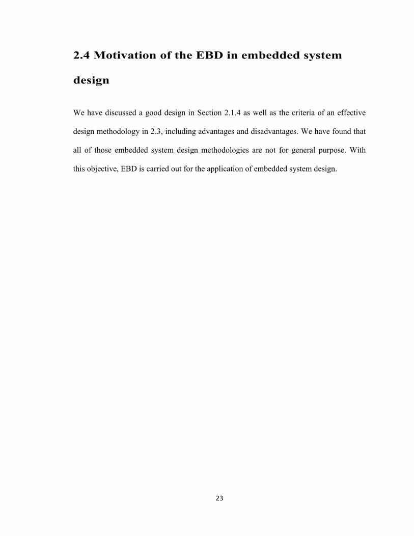
However, people often fail at the first step: understanding the design problems. Figure
10 shows how important it is to understand design requirements correctly.
Figure 10 Illustration of problems existing in software product development [38]
According to Standish Group statistical data, only 16.2% of software projects are
completed on time and within the budget. The website It-cortex concludes that only 1
out 5 IT projects is likely to bring full satisfaction and only 16.2% of software projects
that are completed on-time and on-budget bring full satisfaction [38].
In the following section, a step-by-step guide is presented to show how to apply EBD to
an embedded product design.

30
3.3 Understanding design problems: embedded
product life cycle environment analysis
No matter whether you apply EBD to embedded system design or not, without doubt, to
understand what to do is the first thing for a developer dealing with an embedded system
design. According to EBD, the purpose of environment analysis is to understand design
problems. In other words, the purpose is to understand design requirements early and in
a right way by analyzing the product working environment in its life cycle from nature,
to the built, human environment.
In embedded system engineering, design requirements or specifications are often
verbally received from other design engineers or users. No matter what other design
requirements are, they should finally be changed into technical design requirements. The
developer will often then create code that handles the specifications. The author has
learned from experience that development time is very often longer than expected
because of testing, validating, debugging, redesigning, and redefining the design
requirements.
Let us start with a simple embedded system design example to understand it. We start
with a simple word to describe the objective of the expected embedded product
according to the understanding of the concept.
31
Objective:
Objective 0: develop a machine to do something (verbally received embedded system
design requirements).
Very often, the objective for the design is given by someone who may know very little
about computer systems or the real meaning of an embedded system. Or he/she does not
have any knowledge of embedded system design. He/she just expresses this objective to
professionals, asking generic questions.
Objective 1(transferred into technical design requirements):
(1) Develop embedded hardware;
(2) and develop embedded software
to initialize hardware components;
to load binary images to target the board;
to load images from a loading address to a running address;
to manage electronic components;
to boot up a system;
to provide a service to the user;
to provide distributed individual online updating features for some images.
This is a general development objective description for the remote station (the embedded
system), shown in Figure 6 above. To better understand design problems including
hidden problems, the following general questions would be recommended in the next

32
section, namely Step 2.
Step 1: Create a ROM diagram from the initialized design/development objective.
Figure 11 Created first ROM diagram
This first ROM diagram shown above in Figure 11 was created for the initialized
design problem: verbally received embedded system design requirements.
We recommend generating a ROM from your answer rather than your questions
because the purpose of generating a ROM is the following:
To get what a user really needs by asking the right questions and
collecting the right answers.
To find the key components.
Having transferred the technical design requirements shown above from a natural
language, we now create it in an updated ROM diagram (Figure 12).

33
Figure 12 Created first updated ROM diagram
Figure 12 above was created first as an updated ROM diagram to initialize the
design problem: having changed it into technical design requirements.
According to EBD (rules for objects analysis), for example, from ROM Figure
11 above, we already know the key environment components - machine and
something. The reason is that - for “machine”, there is one constraint relationship
and one predicate relation; for “something” there is one predicate relation and
one connection relation.

34
Similarly, in Figure 12 ROM above, using Rules for object analysis according to
EBD, you may have key environment components: an embedded system,
hardware components, binary images, and images from a loading address to a
running address, some electronic components, and the system, service and
distributed online updating feature for each image.
Then taking the following steps, we ask the right generic questions and the
specific questions. Professionals may ask better but fewer questions than non-
professionals. However, non-professionals are still able to ask concept and
preliminary design questions. For a detailed development, non-professionals may
not be able to give the right answers in some cases.
Step 2: Ask generic questions and collect answers and then repeat
until no more generic questions can be asked.
According to EBD, rules for generic questions shown in APPENDIX, as follows:
Table 1 Rules for generic questions[39]
Rule 1 Before an object can be further defined, the objects constraining them
should be defined.
Rule 2 An object with the most undefined constraints should be taken care of
first.
35
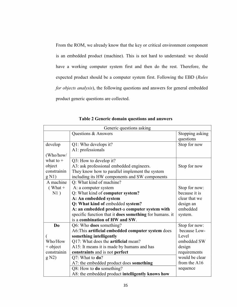
From the ROM, we already know that the key or critical environment component
is an embedded product (machine). This is not hard to understand: we should
have a working computer system first and then do the rest. Therefore, the
expected product should be a computer system first. Following the EBD (Rules
for objects analysis), the following questions and answers for general embedded
product generic questions are collected.
Table 2 Generic domain questions and answers
Generic questions asking
Questions & Answers Stopping asking
questions
develop
(Who/how/
what to +
object
constrainin
g N1)
Q1: Who develops it?
A1: professionals
Stop for now
Q3: How to develop it?
A3: ask professional embedded engineers.
They know how to parallel implement the system
including its HW components and SW components
Stop for now
A machine
( What +
N1 )
Q: What kind of machine?
A: a computer system
Q: What kind of computer system?
A: An embedded system
Q: What kind of embedded system?
A: an embedded product-a computer system with
specific function that it does something for humans. it
is a combination of HW and SW.
Stop for now:
because it is
clear that we
design an
embedded
system.
Do
(
Who/How
+ object
constrainin
g N2)
Q6: Who does something?
A6:This artificial embedded computer system does
something intelligently
Q17: What does the artificial mean?
A15: It means it is made by humans and has
constraints and is not perfect
Stop for now:
because Low-
Level
embedded SW
design
requirements
would be clear
from the A16
sequence
Q7: What to do?
A7: the embedded product does something
Q8: How to do something?
A8: the embedded product intelligently knows how

36
to do something and what to do.
(Once powered up, it can do what human products can
do for humans)
Q18: How to do it intelligently?
A16: developers design a number of SW modules
telling it what to do by following a certain sequence :
1. Power up
Example of an additional question: how to power up
the system? How to code it?
2. Run Boot loader
Example of additional questions: how/where to run
boot loader?
3. Load kernel to running address
Example of additional question: how/where to load?
4. Run kernel
Example of an additional question: how/where to run?
5. Find ROOTFS and then run applications
Example of additional question: how/where to find
and run it?
Something
( What
+N2)
Q9: What is the something?
A9: something means the specific function of the
system
Something means this product is a computer system
with specific functions instead of a computer system
with a general function, and it knows what /how to do.
In another words, humans wanted the artificial
embedded computer system to perform something for
humans intelligently. From the technical point of
view, it is the job of the applications to perform this.
What specific function?
A14: special function means it executea a specific
code and is able to do this and/or that as the user
requires .This and that in here is what you want this
product to do.
Stop for now:
because what
high level
applications
needed would
be clear for now
With answers collected by asking the generic domain questions, in order to ask
more right question after this stage, you should update a ROM diagram from the
generic domain answers. At this point, do not update this ROM because the goal
in the present paper is just to show the concept of applying EBD to an embedded
system design.

37
Step 3: Ask specific domain questions and collect answers and then
repeat until no more generic questions can be asked.
This stage is to get the detailed design requirements. According to EBD (Rules for
asking domain specific questions[39], as discussed in the last section, to get
detailed design requirements, we should understand that:
1. The product design requirements should be analyzed at each event in its life
cycle[37]
In a different embedded product design such as different devices design, its life cycle
may encounter different events. For example, you may divide your product
life=cycle events into design /development, test and debug, software=based HW
components testing for manufacturing, manufacturing, sale, transportation, use,
maintenance and recycling. Figure 13, which follows, is just an example.
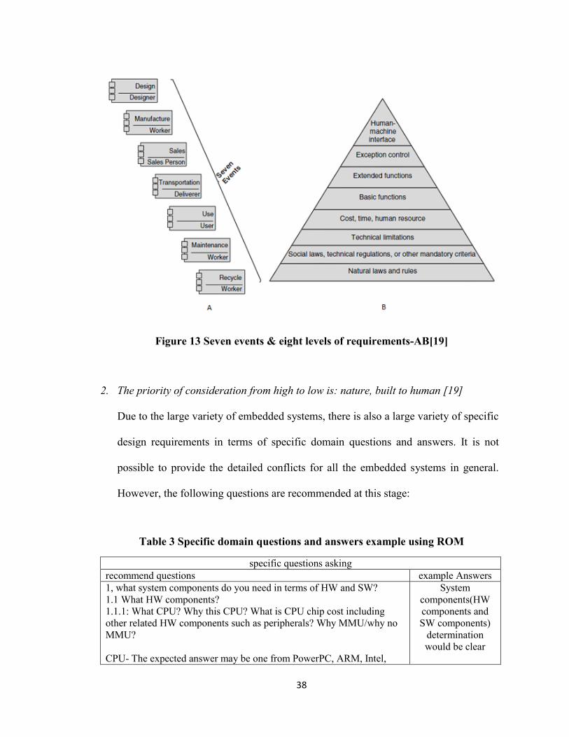
38
Figure 13 Seven events & eight levels of requirements-AB[19]
2. The priority of consideration from high to low is: nature, built to human [19]
Due to the large variety of embedded systems, there is also a large variety of specific
design requirements in terms of specific domain questions and answers. It is not
possible to provide the detailed conflicts for all the embedded systems in general.
However, the following questions are recommended at this stage:
Table 3 Specific domain questions and answers example using ROM
specific questions asking
recommend questions example Answers
1, what system components do you need in terms of HW and SW?
1.1 What HW components?
1.1.1: What CPU? Why this CPU? What is CPU chip cost including
other related HW components such as peripherals? Why MMU/why no
MMU?
CPU- The expected answer may be one from PowerPC, ARM, Intel,
System
components(HW
components and
SW components)
determination
would be clear

39
AMD, MIPS, M68k, COLDFIRE, AVR, M32C, PIC, RL78, SHARC,
SPARC, ST6, MCS-51 etc.
1.1.2: What memory? What size? SRAM size and expected images
footprint? SDRAM size and expected images footprint? What flash? No
flash? NAND flash? SD card? EEPROM? Why this flash? What type?
Size? Or flash with XIP?
1.1.3 What peripherals? What network? Blue tooth? GPS? What
drivers?
1.2 What SW components?
1.2.1 What SW images? Elf or Bin?
1.2.2 What Boot Loader image? U-boot? Grub?
1.2.3 What kernel image? BZIMAGE or other?
1.2.4 What ROOTFS image? CRAMFS, ext2...?
1.2.5 What applications? Video player or what?
1.2.6 What restrictions on the SW and so on?
1.2 What operating system do we need?
The expected answer may be Linux, Windows CE, VXWORKS, and
android and so on.
1.2.1The cost of the OS in terms of the related SW module including
drivers and so on?
1.2.2 What version?
Possible answers are Linux 2.4, 2.6 and so on.
1.2.3What modules do we need to develop?
1.2.4 What interface do we have or need?
1.2.5 What drivers do we need?
1.2.6 Do we need a real time operating system (RTOS)?
1.2.7 Do we really need operating system OS or no OS?
Mostly we use OS but some outdated simple systems do not. You may
have more questions like: Why do we need an OS and why not?
What operating
system and drivers
needed would be
use is clear
1.3 Develop Boot Loader or use existing open source?
Ex: Why develop it u-boot?
1.3.1 If the OS may be updated into another OS in the future, can your
loader be applied?
1.3.2 Development cost?
1.3.3 Open source cost for Boot Loader?
1.3.4 What perimeter to transfer to kernel if using u-boot?
1.3.5 What size limitation?
design
requirements
would be clear for
now
1.4 Do we need to develop a ROOTFS or can we use open source?
Ex: Why yes?
Why not?
design
requirements
would be clear for
40
now
1.5 What applications do we need?
design
requirements
would be clear for
now
1.6 How to boot up the system?
1.6.1 How to power up the system?
1.6.2 Push a button or not?
1.6.3 Execute specific code from CPU specific offset?
1.6.4 How to run boot loader?
1.6.5 Which memory location will execute which specific program?
1.6.6 How to load kernel to running address?
1.6.7 Where is the running address for xx image?
1.6.8 Where is loading address for xxx image?
1.6.9 If bad block in loading address of flash, what to do?
1.6.10 How to run kernel?
1.6.11 How to run applications?
Boot up app would
be clear
1.7What is the life cycle of the embedded product?
Design
requirements
would be from life
cycle of the
product
1.8What are constraints for each event of the product life cycle?
1.9What constraints for the system?
Example: Will a radiation environment affect the system’s functioning?
other constraints ...
What constraints
would be clear
We stop to ask questions once the design requirements are clear. We do not give
a detailed answer because of the large variety of embedded systems. For
example, in embedded product development, it may not be possible to use open
source and therefore the boot loader will have to be customized. Then you will
have your own answer. There would be more detailed questions asked in the
specific questions stage according to your product. At this point, it is enough to
just show a general process of how to apply an EBD to the embedded product
design process.

41
So far, by asking specific domain questions, the HW components should be
determined to use, including CPU and memory, for the remote station system.
We also have embedded remote station system SW components determination
including OS, file system, loaders, and applications and so on. In addition, we
have low level embedded remote station system SW design requirements. Next,
it is time to do the HW development and the SW coding. At this point, you
should also have an updated ROM from your answers. We do not refer to an
updated ROM for asking specific domain questions because of the large variety
of embedded systems.

42
According to EBD, the following Table 4 is recommended to determine the design
requirements including hidden design requirements in the product life cycle (from Event
#1# to Event #n#), for example, in the following Table 4, conflicts and constraints.
Table 4 Lifecycle analysis of the embedded product design problem- specific domain
questions
Events
in life
cycle of
embedde
d
product
embedded
product
nature
environme
nt in life
cycle
Your
embedded product
built environment
in life cycle
Your
embedded product
human environment
in life cycle
Nature
law and
rules
Social
law,
technical
regulatio
ns, or
other
criteria
Technic
al
limitatio
ns
Cost,
time,
human
resourc
e
Basic
functio
ns
Exten
ded
functi
ons
Except
ion
control
Human
machine
interface
Event 1#
E1N1
Constraint
s 1N1
E1B1
Constraints 1B1
E1H1
Constraints 1H1
Event 2#
E2N2
Constraint
s 2N2
E2B2
Constraints 2B2
E2H2
Constraints 2B2
... ... ... ...

43
In Table 4, EiNi / EiBi / EiHi represent event i# in its environment component:
What is the design requirement from the product’s natural environment, the
product’s built environment, and /or the product’s human environment?
What Constraints N, Constraints B and /or Constraints B do we have in Event #.
In Table 4 above, for the remote embedded station system, we find the following
conflicts shown in the Table 5 in the next section.
3.4 Analyzing design problems: conflict
identification in embedded product life cycle
Due to the large variety of embedded systems, there is also a large variety of conflicts. It
is not possible to provide the detailed conflicts for all embedded systems in general.
However, in this section, give some reasonable and commonly seen examples of
conflicts. The case study used in this chapter shows a designer how to apply EBD to an
Event #
EiNi
Constraint
s N
EiBi
Constraints B
EiHi
Constraints B
Event n#
EnNn
Constraint
s n N n
EnBn
Constraints n B n
EnHn
Constraints n B n

44
embedded concept system design. It will be validated by looking at the detailed
development process in the next chapter.
The conflict identification example, for the embedded remote station system design, is
used to show how to use EBD in the concept design process. This is introduced at the
beginning of this chapter. Again, due to the large variety of embedded systems, there
may be many conflicts due to the variety of different products.
After the specific domain questions and answers given in Table 4, there may be a
number of conflicts as shown in Table 5:
(1) Conflict identification
Table 5 Conflict identification
Name Conflicts Description
CI-1 Size /weight many chips
User wants the product size to be small and does not want
the product to be too heavy ; but to achieve this, many
electronic components must be used and therefore the
PCB board would be big.
CI-2
Less
memory
more
memory
To satisfy the user with a low price, we have to make
product cost less. To save product cost, we have to use
less memory. To have better product performance and
features, we have to implement additional features using
45
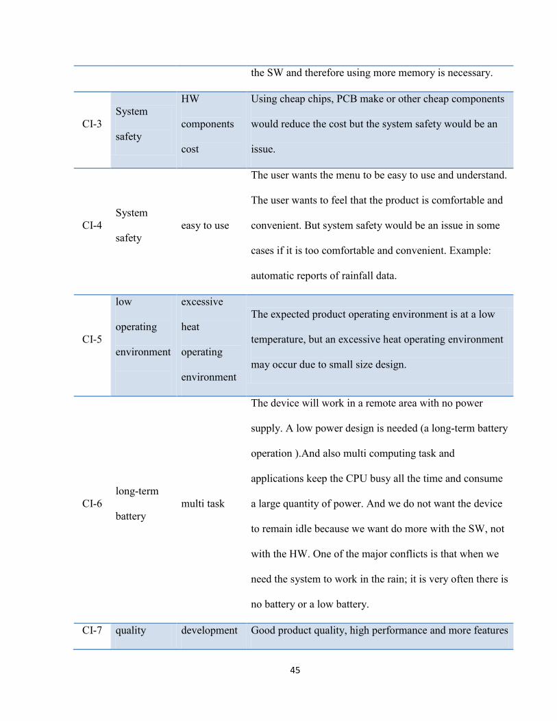
the SW and therefore using more memory is necessary.
CI-3
System
safety
HW
components
cost
Using cheap chips, PCB make or other cheap components
would reduce the cost but the system safety would be an
issue.
CI-4
System
safety
easy to use
The user wants the menu to be easy to use and understand.
The user wants to feel that the product is comfortable and
convenient. But system safety would be an issue in some
cases if it is too comfortable and convenient. Example:
automatic reports of rainfall data.
CI-5
low
operating
environment
excessive
heat
operating
environment
The expected product operating environment is at a low
temperature, but an excessive heat operating environment
may occur due to small size design.
CI-6
long-term
battery
multi task
The device will work in a remote area with no power
supply. A low power design is needed (a long-term battery
operation ).And also multi computing task and
applications keep the CPU busy all the time and consume
a large quantity of power. And we do not want the device
to remain idle because we want do more with the SW, not
with the HW. One of the major conflicts is that when we
need the system to work in the rain; it is very often there is
no battery or a low battery.
CI-7 quality development Good product quality, high performance and more features

46
time are needed. To have quality product, we have to have
more time to do it.
to release product earlier, we have to reduce development
time
CI-8 Small size
excessive
heat
If the size is too small, in a hot environment, the
components would be running at an unsafe operating
temperature and therefore the integrated circuits such as
CPU and other chips would be damaged.
CI-9 Speed heat
The user wants high speed. But a fast running CPU may
generate excessive heat, an effect which is not wanted.
CI-10
More SW
tasks; Do
more thing
using SW,
not HW
Heat and
system
reliability
We want both low heat and more SW tasks running.
Because of our cost saving goal, we design embedded
products using the SW to do as much as we can instead of
the HW. When no task is running, the system can be put to
sleep. However, more tasks cause a heat increase, and this
increased heat risks the safety of electronic components
safety, and in addition system safety. Also, more and
complicated SW tasks may bring about some potential
bugs or other deadlocks to the system. This would threaten
the system reliability.
CI-11 Price cost
Lower price is needed because user wanted. But product
cost may be high.
CI-12 Do more Less memory On the one hand, we want to do more things using SW,

47
thing using
SW, not
HW
not HW because of cost; on the other hand, we want to use
less memory (SRAM, SDRAM, flash...) to save product
cost.
(2) Conflict relationships analysis
Figure 14 shows all the relationships between all the conflicts from CI-1 to CI-12.
CI-1#
CI-4#
CI-6#
CI-3#
CI-12#
CI-10#
CI-8# CI-7#
CI-2#
CI-9#
CI-11# CI-5#
Figure 14 Conflict relationships analysis: an example
48
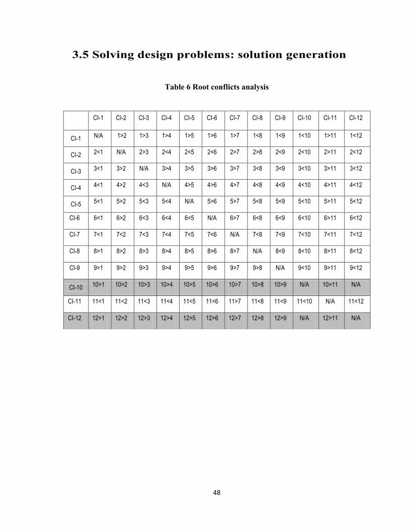
3.5 Solving design problems: solution generation
Table 6 Root conflicts analysis
CI-1 CI-2 CI-3 CI-4 CI-5 CI-6 CI-7 CI-8 CI-9 CI-10 CI-11 CI-12
CI-1 N/A 1>2 1>3 1>4 1>5 1>6 1>7 1<8 1<9 1<10 1>11 1<12
CI-2 2<1 N/A 2>3 2<4 2<5 2<6 2>7 2>8 2<9 2<10 2>11 2<12
CI-3 3<1 3>2 N/A 3>4 3>5 3>6 3>7 3<8 3<9 3<10 3>11 3<12
CI-4 4<1 4>2 4<3 N/A 4>5 4>6 4>7 4<8 4<9 4<10 4>11 4<12
CI-5 5<1 5>2 5<3 5<4 N/A 5>6 5>7 5<8 5<9 5<10 5>11 5<12
CI-6 6<1 6>2 6<3 6<4 6<5 N/A 6>7 6<8 6<9 6<10 6>11 6<12
CI-7 7<1 7<2 7<3 7<4 7<5 7<6 N/A 7<8 7<9 7<10 7<11 7<12
CI-8 8>1 8>2 8>3 8>4 8>5 8>6 8>7 N/A 8<9 8<10 8>11 8<12
CI-9 9>1 9>2 9>3 9>4 9>5 9>6 9>7 9>8 N/A 9<10 9>11 9<12
CI-10 10>1 10>2 10>3 10>4 10>5 10>6 10>7 10>8 10>9 N/A 10>11 N/A
CI-11 11<1 11<2 11<3 11<4 11<5 11<6 11>7 11<8 11<9 11<10 N/A 11<12
CI-12 12>1 12>2 12>3 12>4 12>5 12>6 12>7 12>8 12>9 N/A 12>11 N/A
49
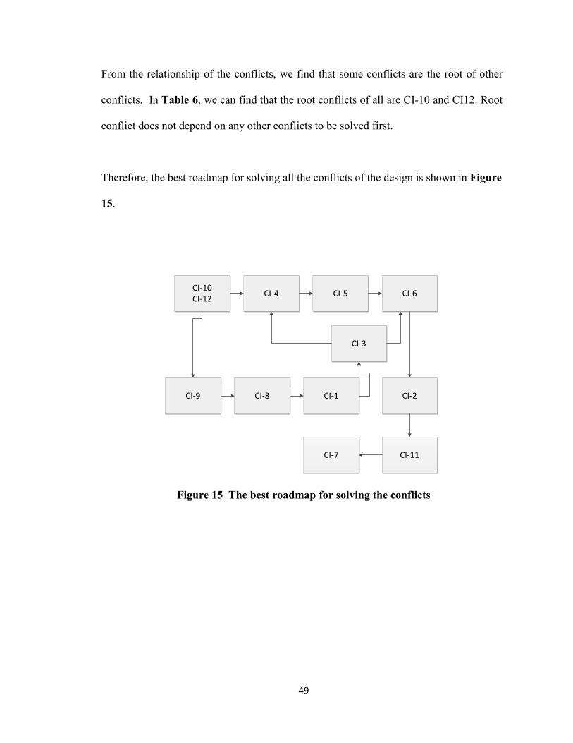
From the relationship of the conflicts, we find that some conflicts are the root of other
conflicts. In Table 6, we can find that the root conflicts of all are CI-10 and CI12. Root
conflict does not depend on any other conflicts to be solved first.
Therefore, the best roadmap for solving all the conflicts of the design is shown in Figure
15.
CI-10CI-12
CI-4 CI-5 CI-6
CI-9 CI-8 CI-2
CI-11CI-7
CI-1
CI-3
Figure 15 The best roadmap for solving the conflicts

50
Chapter 4
VALIDATION OF EBD:
EMBEDDED PRODUCT
DEVELOPMENT - A CASE
STUDY
In Chapter 3, from a general point of view, we dealt with the application of the EBD to
embedded system concept design and how to use the EBD in the embedded system
design process.
In this chapter, instead of showing how to use EBD in an embedded system concept
design as we did in the last chapter, we use a detailed embedded system development of
the case study mentioned in Chapter 3 to discuss rainfall and the control of the level of
water for the local residents to validate EBD design methodology.
51
4.1 Introduction
4.1.1 Additional case review
As mentioned in the last chapter, the remote station embedded system in this case study
consists of collecting data about the level of rainfall and water in reservoirs and then
sending the data to a server.
The systems track natural rainfall and water levels in the local and nearby reservoirs (or
a river, or a lake). The purpose for such tracking is to avoid drought and flood disaster
caused by too little or too much rain. The function of the embedded remote station
system is to collect signals from the two sensors: the rainfall sensor and the water-level
sensor. After being dealt with by the system, the signals are sent to a central station
(server) by the network.
That embedded remote station system is the one designed in the case study.
The system works according to the following rule:
Rule 1: No matter whether the level of water in the reservoirs (or a river, or a lake) is
normal or abnormal, once it rains the system keeps sending data to the central
station. Once the level of water is abnormal, instead of sending normal data,
the system sends urgent mask messages to the server.
Rule 2: When the level of water in the reservoirs (or a river, or a lake) is abnormal or at

52
a dangerous level, whether it rains or not, the system sends data to the central
station with urgent mask messages and releases some water.
Rule 3: When the water level in some remote station is higher than that in others cases,
the central station sends commands to the remote station to ask the terminal
station system to balance the water level by releasing some water.
Rule 4: When there is no rain AND the water level is at a normal level, the system is put
into a sleep state to save battery life. Once it rains, the system wakes up and
starts to send data to the central station server.
One major conflict for the system is the following: when we need the system to work due
to rain, it is often that there is no battery power or there is a low battery level; the network
throughput is not large enough to send data out as soon as necessary. A low power
design, not only in the HW but also in the SW, is essential. This means that the system
needs to be put into a sleep state to save power when there is no rain and the water level
is normal. However, once it rains, waking up the system takes time.

53
Figure 16 shows the remote station system components.
Figure 16 The remote station system components
4.1.2 Must-do task list for a detailed product development
Whether an EBD is used or not, developing the remote station embedded system, you
have to follow the task lists shown in Table 7 for the new product (a must-do list) for the
detailed development), which is not the concept design discussed in Chapter 3. The
remote station
embedded system components
HW
CPUMemory
RAM
SRAM SDRAM
ROM
flash Other
peripherals
USB RS-232wireless network
wifi Keyboard LCDGPIO
Sensor printer
SW
Boot lader kernel
config drivers app
RootFS Applications

54
detailed development process would be used to validate the EBD.
Table 7 Technical to-do list for the development
Task
name
Task description
(activity description)
Task 1# Design requirements analysis
Task 2# Hardware schematic design including low power design
Task 3# PCB layout design including low power design
Task 4# Develop NAND flash driver including memory layout partition coding
for distributed updating of Bootstrap, U-Boot, u-boot parameters,
kernel, and applications. SD card driver
Task 5# Develop SDRAM driver including reading datasheet and testing
Task 6# Develop U-boot including reading relative code such as start.S, CPU
datasheet , developing relative device drivers and so on
Task 7# Develop kernel including NFS configuration, memory configuration,
file system configuration, I/O configuration and other configuration,
system components selection, coding for some protocols, coding
related applications under /bin and /sbin, coding other SW components
and building kernel and so on
Task 8# Develop necessary kernel device drivers including keyboard device
driver, LED driver, LCD, SD card, sensor, printer, USB, I2C and
water level, rainfall and network device drivers and so on.
Task 9# Develop ROOT file system using BusyBox

55
Task 10# Develop applications such as multi thread applications for multi task
purposes and real time purposes
Task 11# Develop software-based module for memory and other HW
components testing for manufacturing, such as pins short, open or
other issues shown in Figure 17and Figure 18.
Task 12# Validation and verification
Task 13# QA test
Task 14# documentation
This list from 1# to 14# includes what is necessary for an embedded product
development. However, it must be noted that this is not a linear development process
from task number 1# 14#. 1# to 14 # here are just the task names.
4.1.3 Example of a hidden problem
Figure 17 An example of SDRAM mounting – hidden problems

56
Figure 18 An example of results from SDRAM pins problems- effect from a hidden
problem
The first Figure 17 above and the second Figure 18 above show the reason for coding
software-based modules to test hardware components such as SDRAM pins short, open
or other issues. Software-based module development for a hardware components test is
not the only good BSP development but is also good for manufacturing because of
hidden problems.
4.2 Development process without EBD
methodology
4.2.1 Product development process
(1) Task duration in the detailed product development process
Table 8 below shows the product development tasks and their duration without using
EBD. This is NOT a linear development process from task number T1# to task
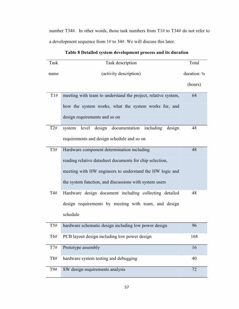
57
number T34#. In other words, those task numbers from T1# to T34# do not refer to
a development sequence from 1# to 34#. We will discuss this later.
Table 8 Detailed system development process and its duration
Task
name
Task description
(activity description)
Total
duration: Tx
(hours)
T1# meeting with team to understand the project, relative system,
how the system works, what the system works for, and
design requirements and so on
64
T2# system level design documentation including design
requirements and design schedule and so on
48
T3# Hardware component determination including
reading relative datasheet documents for chip selection,
meeting with HW engineers to understand the HW logic and
the system function, and discussions with system users
48
T4# Hardware design document including collecting detailed
design requirements by meeting with team, and design
schedule
48
T5# hardware schematic design including low power design 96
T6# PCB layout design including low power design 168
T7# Prototype assembly 16
T8# hardware system testing and debugging 40
T9# SW design requirements analysis 72
58
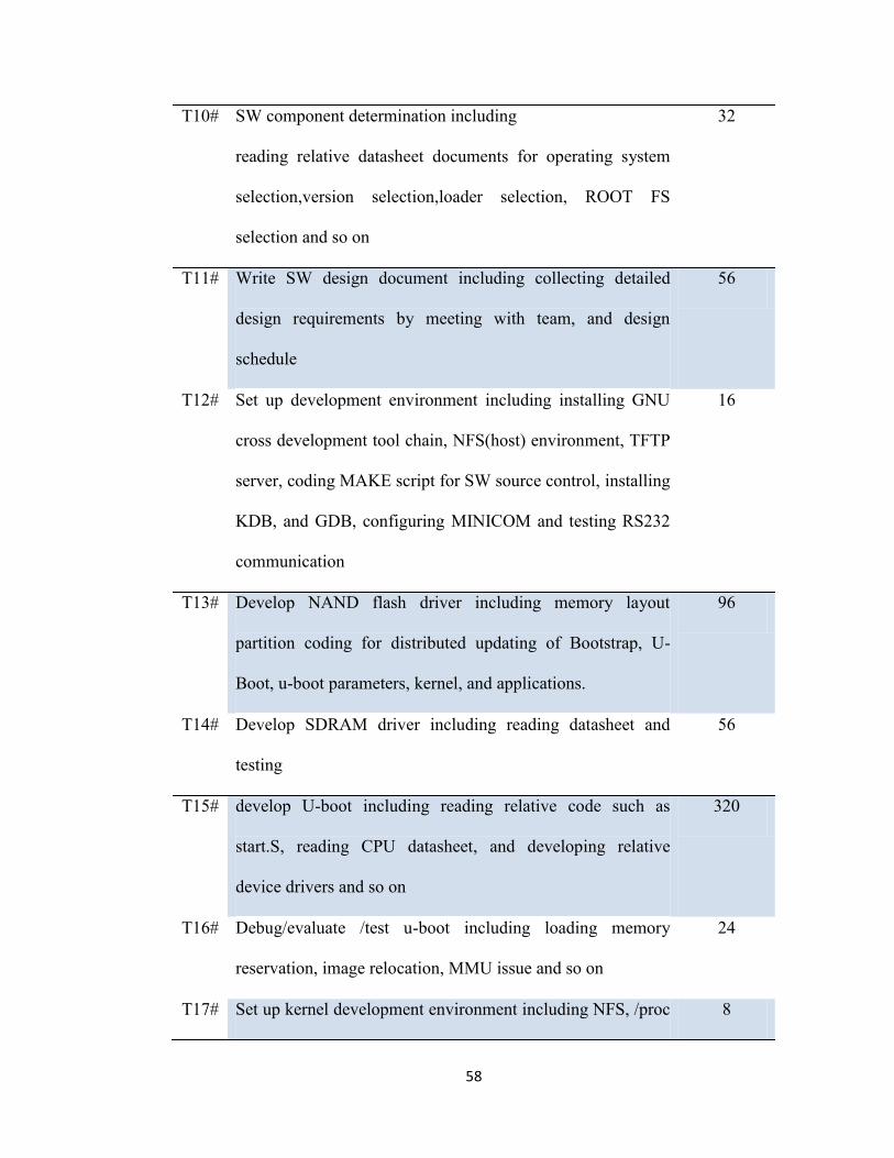
T10# SW component determination including
reading relative datasheet documents for operating system
selection,version selection,loader selection, ROOT FS
selection and so on
32
T11# Write SW design document including collecting detailed
design requirements by meeting with team, and design
schedule
56
T12# Set up development environment including installing GNU
cross development tool chain, NFS(host) environment, TFTP
server, coding MAKE script for SW source control, installing
KDB, and GDB, configuring MINICOM and testing RS232
communication
16
T13# Develop NAND flash driver including memory layout
partition coding for distributed updating of Bootstrap, U-
Boot, u-boot parameters, kernel, and applications.
96
T14# Develop SDRAM driver including reading datasheet and
testing
56
T15# develop U-boot including reading relative code such as
start.S, reading CPU datasheet, and developing relative
device drivers and so on
320
T16# Debug/evaluate /test u-boot including loading memory
reservation, image relocation, MMU issue and so on
24
T17# Set up kernel development environment including NFS, /proc 8

59
file system, and TCL configuration file reinstalling and
relative test and so on
T18# Develop kernel including NFS configuration, memory
configuration, file system configuration, I/O configuration
and other configuration, system components selection,
coding for some protocols, coding relative for applications
under /bin and /sbin, coding other SW components and
building kernel and so on
76
T19# Prototype system test from so-called system-level 24
T20# Develop necessary kernel device drivers (one by one and step
by step) including keyboard device driver, LED driver, LCD,
SD card, sensor, printer, USB, I2C and water level, rainfall
and network device drivers and so on.
312
T21# Develop use space SW modules to test kernel drivers
performance
24
T22# Develop ROOT file system using BusyBox 56
T23# Prototype system test from system level 16
T24# System-level test & debugging from hardware to software
including u-boot, kernel, and ROOT file system. Design of
experience is recommended for the evaluation because bugs
may be from one or more of – HW, u-boot, kernel, and
ROOT file system.
40
T25# Prototype firmware system performance QA test 24
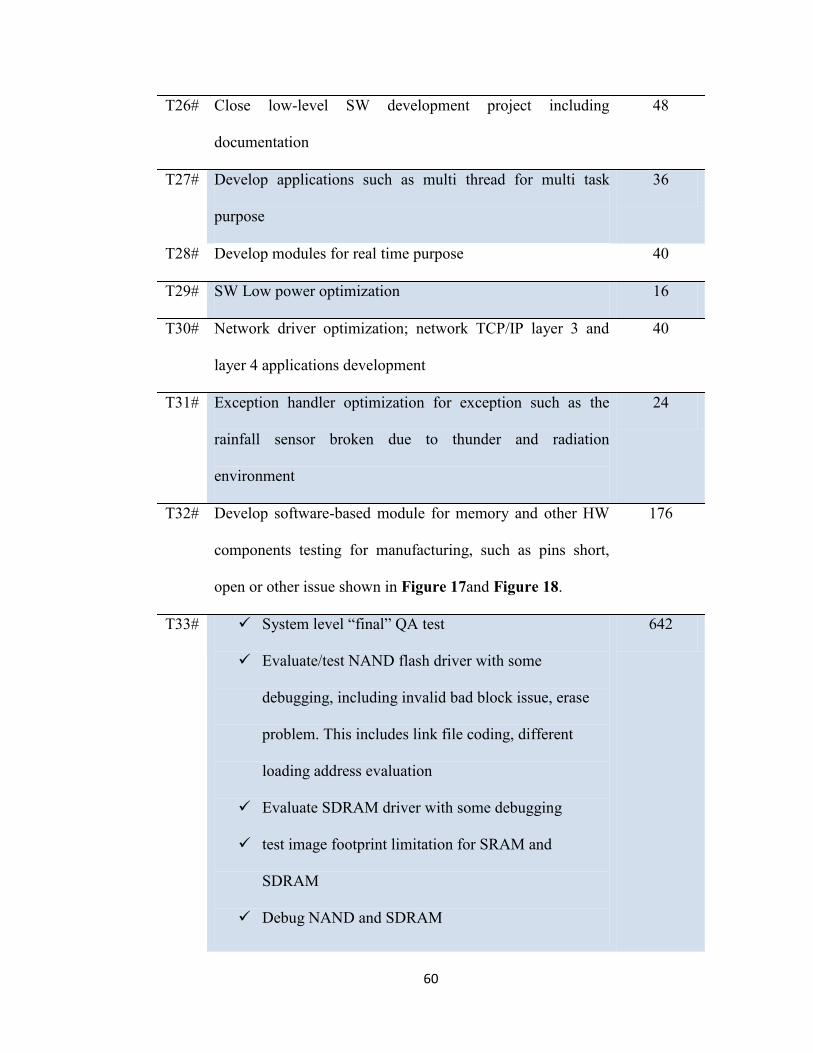
60
T26# Close low-level SW development project including
documentation
48
T27# Develop applications such as multi thread for multi task
purpose
36
T28# Develop modules for real time purpose 40
T29# SW Low power optimization 16
T30# Network driver optimization; network TCP/IP layer 3 and
layer 4 applications development
40
T31# Exception handler optimization for exception such as the
rainfall sensor broken due to thunder and radiation
environment
24
T32# Develop software-based module for memory and other HW
components testing for manufacturing, such as pins short,
open or other issue shown in Figure 17and Figure 18.
176
T33# System level “final” QA test
Evaluate/test NAND flash driver with some
debugging, including invalid bad block issue, erase
problem. This includes link file coding, different
loading address evaluation
Evaluate SDRAM driver with some debugging
test image footprint limitation for SRAM and
SDRAM
Debug NAND and SDRAM
642

61
Hardware system test by using u-boot software (part
of HW only)
Hardware debugging. Example: NAND block can be
erased only at 12V! The power of back-up power
supply (USB) cannot reach expected voltage.
Optimize u-boot by meeting hardware limitation,and
adding/remove some drivers, and tailoring it to a
smaller footprint and so on
Optimize & test kernel for footprint requirement to
meet planed flash memory layout and its partition
Evaluate kernel using u-boot;
Evaluate u-boot using kernel;
Evaluate the hardware system by using u-boot
software and kernel software.
Examples are some kernel device driver VS HW
design
Debug kernel boot-up application and removing
unnecessary section in the image segment for small
footprint purpose
Debug u-boot
Debug hardware system
Optimize some drivers including interrupt handler,
bottom-half, sleep queue, memory allocation, race

62
condition
Test hardware devices and kernel drivers
Debug hardware system and kernel driver
Evaluate kernel using u-boot and ROOT file system
and hardware system;
Evaluate u-boot using kernel and ROOT file system
and hardware system;
Evaluate hardware system by using u-boot software,
kernel software and some of device drivers. Examples
are some kernel device driver VS HW design
Evaluate ROOT file system using u-boot and kernel
and hardware system
System-level debugging from HW to all SW
T34# System documentation 48
Total
time
2850
The task T33# is all about test, investigating, validating, debugging and so on. Debugging
and redesigning take too much time.

63
(2) Development process model
Many embedded designers may follow this development process shown in Figure 19.
Figure 19 Detailed development process without using EBD
SW DEVDesign Requirements Analysis
Design documents
HW target board DEVManufacturingassembly
Design Requirements Analysis
Target board test using hardware
tool
Boot loader NAND SDRAM U-boot
…
Kernel DEVKernelDrivers
…
Root file system DEV
Applications DEV
Verification Validation Evaluation / test Hardware debuggingSW debuggingSystem-level debugging/testing/validation …. QA testOptimization such as driver, exception handler … ...
User
What went wrong andWhere is the source ?
Who are variables and who are constants ?
release
Final debugging,verification, validation evaluation / stage test hardware debugging,Software debuggingSystem-level debugging/testing/validation …. QA test, system optimization such as driver, exception handler … ...

64
Everything may go very well with the development process from design requirements
analysis, detail HW & SW development including some small test during the
development process. However, when the design stage comes to the final QA test, many
problems may show up and developers may spend a lot of time debugging, testing, and
redesigning. And, it may be hard to find the problem and where its source is. The reason
is that the developer collects a wide range of distrusted variables in each design stage
without validating what the variables are and what is constant in an earlier stage. This
problem will be discussed later in Section 4.3.
4.2.2 Quality of development process
The results from the development process without applying EBD methodology are
shown in Table 9 below.
Table 9 Result without EBD
Design activity Design
task name
Total
duration
(hours)
Rate
Design requirements
and documentation
1,2,4,9,11 336 11.79%
Detail DEV+ test
( HW & SW )
3,5,6,7,8,10,12,
13,14,15,16,17,
18,19,20,21,22,
23,24,25,26,27,
28,29,30,31,32
1872 65.68%
Final debugging verification,
validation, test and evaluation
and so on
33 642 22.53%
Total 2850 100%

65
The total development time used for the product is 2850 hours. This development time is
absolutely too long. This speed would not satisfy the company.
4.3 Analyzing and diagnosing the development
process using EBD
4.3.1 Adjustment of the development process using EBD
Table 10, Table 11 and Table 12 below show the product development tasks and their
duration with the adjustment of EBD methodology. With EBD, the development
process is composed of sixteen design states from S0 to S15.
With EBD adjustment, task duration in the detailed product development process is
Tx'=Tx± ∆.
Where ,
Tx' is the task duration in the detailed product development process with EBD
adjustment.
Tx is the task duration without using EBD.
∆ is the time difference between those two approaches.
(1) Analyzing the phase one of the development process using EBD

66
In the phase one of the development process, it is mainly about:
System level design requirements analysis
HW design requirements , system components selection , and HW
implementation including small debugging using HW tool
SW design requirements , system components selection , and SW design
environment implementation
There are four design states in the phase : S0, S1, S2, and S3.
Table 10 below shows the product development tasks and their duration with the
adjustment of EBD methodology.
Table 10 EBD analysis for phase one
Design
state /Task
name
Task description
(activity description)
Total
duration:
Tx'=Tx± ∆
(hours)
S0(T1') Meeting with team to understand the project, related system,
how the system works, what the system works for, and design
requirements
64
S0(T2') system level design documentation including design
requirements and design schedule
48
S1(T3') Hardware component determination including
reading relative datasheet documents for chip selection,
meeting with HW engineers to understand the HW logical and
the system function and talking to system users
40

67
S1(T4') Hardware design document including collecting detail design
requirements by meeting with team, and design schedule
48
S1(T5') hardware schematic design including low power design 88
S1(T6') PCB layout design including low power design 144
S1(T7') Prototype assembly 16
S2(T8') hardware system testing and debugging 24
S3(T9') SW design requirements analysis 72
S3(T10') SW component determination including
reading related datasheet documents for operating system
selection, version selection, loader selection, ROOT FS
selection
32
S3(T11') Write SW design document including collecting detail design
requirements by meeting with team, and design schedule
56
S3(T12') Set up development environment including installing GNU
cross development tool chain, NFS(host) environment, TFTP
server, coding MAKE script for SW source control, installing
KDB, and GDB, configuring MINICOM and testing RS232
communication.
16
Total time 648

68
(2) Diagnosing the phase two of the development process using EBD
In phase two of the development process, it is mainly about:
SW detailed development including HW co-design
HW / SW test, evaluation, optimization, debugging
There are four design states in the phase : S4, S5,S6,S7,S8,S9,S10,and S11.
Without using EBD, when the design stage comes to the final QA test, it may be hard
to find the problem and where its source is. Therefore, developers may spend a lot of
time debugging, testing, and redesigning. As discussed in last section, the reason is
that the developer collects a wide range of distrusted variables in each design stage
without validating what the variables are and what is constant in an earlier stage. So,
EBD helps a designer validate the product environment by testing some possible
situation, investigating a hidden problem, validating or evaluating the designer’s
thinking. For example, it may require adding your relocation code into a good loader
to see if it works. This is to evaluate if the relocation code really works before taking
next action.
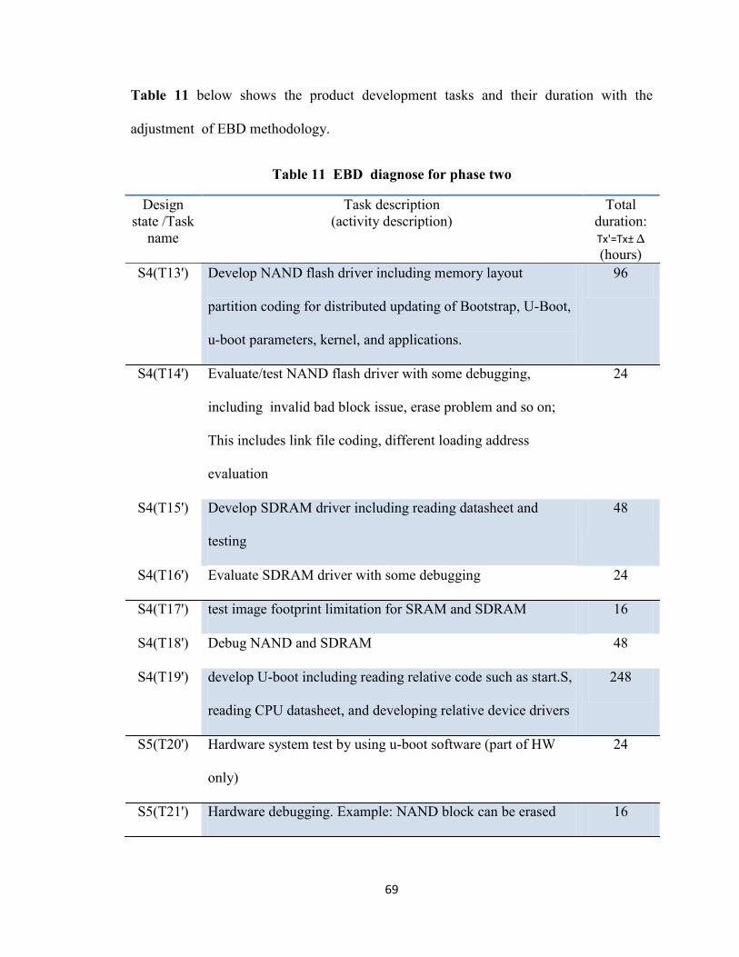
69
Table 11 below shows the product development tasks and their duration with the
adjustment of EBD methodology.
Table 11 EBD diagnose for phase two
Design
state /Task
name
Task description
(activity description)
Total
duration:
Tx'=Tx± ∆ (hours)
S4(T13') Develop NAND flash driver including memory layout
partition coding for distributed updating of Bootstrap, U-Boot,
u-boot parameters, kernel, and applications.
96
S4(T14') Evaluate/test NAND flash driver with some debugging,
including invalid bad block issue, erase problem and so on;
This includes link file coding, different loading address
evaluation
24
S4(T15') Develop SDRAM driver including reading datasheet and
testing
48
S4(T16') Evaluate SDRAM driver with some debugging 24
S4(T17') test image footprint limitation for SRAM and SDRAM 16
S4(T18') Debug NAND and SDRAM 48
S4(T19') develop U-boot including reading relative code such as start.S,
reading CPU datasheet, and developing relative device drivers
248
S5(T20') Hardware system test by using u-boot software (part of HW
only)
24
S5(T21') Hardware debugging. Example: NAND block can be erased 16

70
only at 12V! The power of back-up power supply (USB)
cannot reach expected voltage.
S5(T22') Debug/evaluate/test u-boot including loading memory
reservation, image relocation, MMU issue
24
S5(T23') Optimize u-boot by meeting hardware limitation, and
adding/remove some drivers, and tailoring it to a smaller
footprint
40
S6(T24') Set up kernel development environment including NFS, /proc
file system, and TCL configuration file reinstalling and
relative test
8
S6(T25') Develop kernel including NFS configuration, memory
configuration, file system configuration, I/O configuration and
other configuration, system components selection, coding for
some protocols, coding relative for applications under /bin and
/sbin, coding other SW components , building kernel
68
S6(T26') Optimize & test kernel for footprint requirement to meet
planed flash memory layout and its partition
40
S7(T27') Evaluate kernel using u-boot;
Evaluate u-boot using kernel;
Evaluate hardware system by using u-boot software and kernel
software.
Examples are some kernel device driver VS HW design
40
S89(T28') Debug kernel boot-up application and removing unnecessary 40

71
section in the image segment for small footprint purpose
Debug u-boot
Debug hardware system
S89(T29') Prototype system test from so-called system-level 24
S10(T30') Develop necessary kernel device drivers (one by one and step
by step) including keyboard device driver, LED driver, LCD,
SD card, sensor, printer, USB, I2C and water level, rainfall
and network device drivers.
312
S10(T31') Optimize some drivers including interrupt handler, bottom-
half, sleep queue, memory allocation, race condition.
76
S10(T32') Develop use space SW modules to test kernel drivers
performance
24
S10(T33') Test hardware devices and kernel drivers 24
S10(T34') Debug hardware system and kernel driver 40
S11(T35') Develop ROOT file system using BusyBox 48
S11(T36') Evaluate kernel using u-boot and ROOT file system and
hardware system;
Evaluate u-boot using kernel and ROOT file system and
hardware system;
Evaluate hardware system by using u-boot software, kernel
software and some of device drivers. Examples are some
kernel device driver VS HW design.
Evaluate ROOT file system using u-boot and kernel and
48

72
hardware system
S11(T37') Prototype system test from system level 8
S11(T38') System-level test & debugging from hardware to software
including u-boot, kernel, and ROOT file system. Design of
experience is recommended for the evaluation because bugs
may be from one or more of – HW, u-boot, kernel, and ROOT
file system.
32
S11(T39') Prototype firmware system performance QA test 16
S11(T40') Close low-level SW development project including
documentation
40
Total time 1184
(3) Adjustment of the phase three of the development process using EBD
Table 12 below shows the product development tasks and their duration with the
adjustment of EBD methodology.
Table 12 EBD analysis and diagnose for phase three
Design
state /Task
name
Task description
(activity description)
Total
duration:
Tx'=Tx± ∆
(hours)
S12(T41') Develop applications such as multi thread for multi task 24
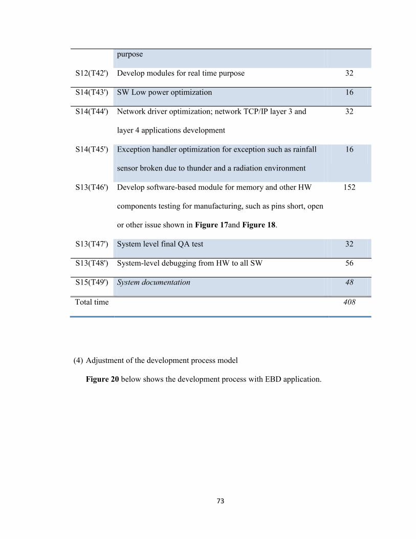
73
purpose
S12(T42') Develop modules for real time purpose 32
S14(T43') SW Low power optimization 16
S14(T44') Network driver optimization; network TCP/IP layer 3 and
layer 4 applications development
32
S14(T45') Exception handler optimization for exception such as rainfall
sensor broken due to thunder and a radiation environment
16
S13(T46') Develop software-based module for memory and other HW
components testing for manufacturing, such as pins short, open
or other issue shown in Figure 17and Figure 18.
152
S13(T47') System level final QA test 32
S13(T48') System-level debugging from HW to all SW 56
S15(T49') System documentation 48
Total time 408
(4) Adjustment of the development process model
Figure 20 below shows the development process with EBD application.
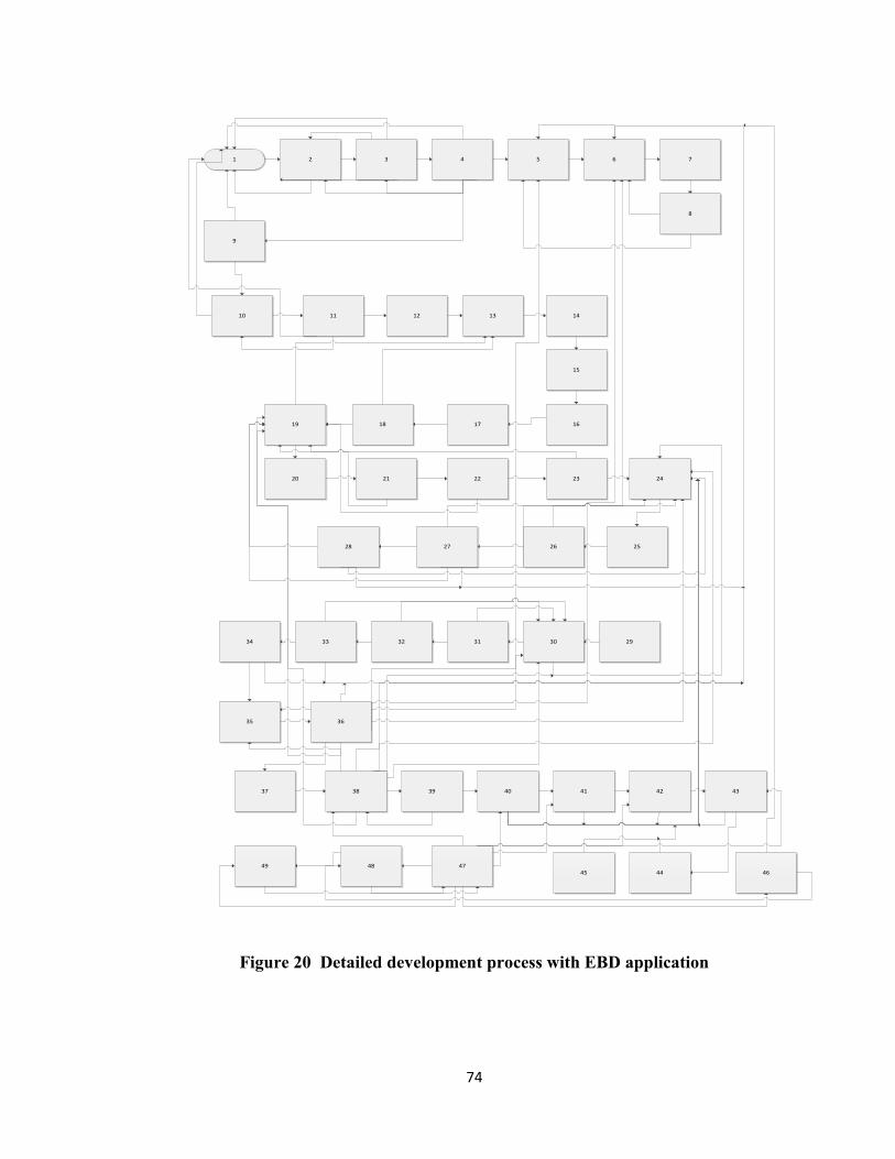
74
1 2 3 4 5 6 7
8
9
10 11 12 13 14
15
16171819
20 21 22 23 24
28 27 2526
35
34 33 32 31 30 29
36
37 38 39 40 41 42 43
4748464445
49
Figure 20 Detailed development process with EBD application

75
4.3.2 Design state
TIME
STATE
E0 Design requirements MeetingDOC
E1HW determinationSCH DEVPCB DEV
E2 Unknown
HW PROTOTYPE
E3 SW determination
Doc DEV preparation
E4 SW DEVTest +debug MEM+CPU+u-boot
E5 SW+HWtest & debug
E6Kernel DEV
E7EvaluationSW+HW
E8+E9 PROTOTYPE System
test SW test
E10 Kernel driver DEV
E11HW test Driver testlow-level SW testQA test
System level test & evaluate & debugging
E12 Application DEV
E14 Optimization
Low – level SW +APP + Exception
Final QA+ debugging
E13 SW DEV manufacturing
Software-based hardware components test for manufacturing
E15Released final product
Y-A
xis
x-Axis
Figure 21 Design state & development time
To sum up the design components in the development process shown in Figure 20 above,
we find that the design process shows the spiral evolution of design as shown in Figure
21 above.

76
Next, explain the detailed design state including the product design environment and the
product design state in the following from (1) to (15).
Where, X-Variables-distrusted environment component, meaning it is not confirmed and
tested.
For example, when software receives a target board from the hardware department, it is
an unknown state of a prototype (Variables); it may be tested by hardware engineers but
not validated by SW code.
C-Constant -trusted environment component, meaning it is fully tested and fully trusted.
(1) Design state 0(S0): task 1#, 2 #
a. Product Design Environment 0(E0)
E0= 𝑥0𝑖𝑖1 = 𝑋01 + 𝑋02 + 𝑋03+𝑋04
Where,
𝑋01 = design requirements, distrusted variable
𝑋02= design documents, distrusted variable
𝑋03=(efficacy of )meetings, distrusted variable;
77
b. Product design state
S0= E0= 𝑥0𝑖𝑖1 = 𝑋01 + 𝑋02 + 𝑋03
This state initialized the design problem and it may not be the real expected problem and
may need to be redefined in the later design process.
(2) Design state 1(S1): task 3#,4#,5#,6#,7#
a. Product Design Environment 1(E1)
E1= 𝑥1𝑖𝑖1 = 𝑋11 + 𝑋12 + 𝑋13+𝑋14+𝑋15
Where,
𝑋11 = Hardware components determination, distrusted variable;
𝑋12 =HW Schematic, distrusted variable;
𝑋13=HW PCB, distrusted variable;
𝑋14 = manufacturing of target board and assembly of target board, distrusted
variable;
𝑋15 =Prototype, distrusted variable;
Where from Hardware components determination, HW Schematic design, HW
PCB design, quality of manufacturing, to prototype assembly, they all may be
78
designed or made wrongly. This may need to be redesigned in the later design
process.
b. Product design state
S1=s0+E1= 𝑥0𝑖𝑖1 + 𝑥1𝑖
𝑖1 =𝑋01 + 𝑋02 + 𝑋03+𝑋11 + 𝑋12 + 𝑋13+𝑋14+𝑋15
In this design state, the designer already has those components: redefined HW design
requirements, relative documents, and the hardware such as HW Schematic, HW PCB
and prototype and so on. But some of them may make troubles.
(3) Design state 2(S2): task 8#
a. Product Design Environment 2(E2)
E2= 𝑥2𝑖𝑖1 = 𝑋21 + 𝑋22 +𝑋23
Where,
𝑋21= unknown state of prototype;
𝑋22= HW test
𝑋23= HW debugging or redesigning
Where HW test (𝑋22) in this stage is using HW tool. Some hiding problem cannot
be found. HW debugging or redesigning (𝑋23) may go to wrong way and change
form good to a bad design for example.

79
b. Product design state S2
S2=E0+E1+E2= 𝑥0𝑖𝑖1 + 𝑥1𝑖
𝑖1 + 𝑥2𝑖
𝑖1 =𝑋01 + 𝑋02 + 𝑋03 +𝑋11 + 𝑋12 +
𝑋13+𝑋14+𝑋15 + 𝑋21 + 𝑋22 +𝑋23
This state, we have an unknown state of prototype because its hidden problem may not be
fully found yet in this stage of design.
(4) Design state 3(S3): task 9#, 10#, 11#, 12#
a. Product Design Environment 3(E3)
E3= 𝑥3𝑖𝑖1 = 𝑋31+𝑋32+𝑋33+𝑋34+𝑋35
Where,
𝑋31= SW components (determination)
𝑋32= design documents
𝑋33= SW development environment structure (DEV ENV setting up)
𝑋34= SW design requirements analysis
𝑋35 =relationship between SW components(determination) and 𝑋11( Hardware
components determination)

80
b. Product design state S3
S3=s2+E3= 𝑥0𝑖𝑖1 + 𝑥1𝑖
𝑖1 + 𝑥2𝑖
𝑖1 + 𝑥3𝑖
𝑖31 =𝑋01 + 𝑋02 + 𝑋03 +𝑋11 + 𝑋12 +
𝑋13+𝑋14+𝑋15 + 𝑋21 + 𝑋22 +𝑋23 +𝑋31+𝑋32+𝑋33+𝑋34+𝑋35
(5) Design state 4 (S4): task 13#, 14#, 15#, 16#, 17#, 18#, and 19#
a. Product Design Environment (E4)
E4= 𝑥4𝑖 𝑖1 + 𝐶4𝑗
𝑗1
𝑥4𝑖 𝑖41 = 𝑋41 + 𝑋42 +𝑋43 + 𝑋44 + 𝑋45 + 𝑋46 + 𝑋47 + 𝑋48 + 𝑋49 + 𝑋410 + 𝑋411 +
𝑋412 + 𝑋413 + 𝑋414 + 𝑋415+𝑋416 +𝑋417
C4jj1 = 𝐶41+𝐶42
Where,
𝑋41=NAND SW code
𝑋42=state of NAND hardware (example : hiding problem such ad invalid block or
data bus Figure 17and Figure 18)
𝑋43 = SDRAM SW code
𝑋44= SDRAM HW state
𝑋45= CPU initialization code
𝑋46= CPU state
𝑋47= SW for boot up

81
𝑋48= relative driver
𝑋49= NAND Evaluation
𝑋410= SDRAM Evaluation
𝑋411 =footprint limitation
𝑋412 = memory debugging
𝑋413 =U-BOOT code
𝑋414 = 𝑈 − 𝑏𝑜𝑜𝑡 𝑖𝑚𝑎𝑔𝑒
𝑋415 =Rrelationships between HW components and SW including u-boot and
NAND code and SDRAM code (the sub-system of the product system )
𝑋416 =test and debugging
𝑋417=unknown or hiding environments ( problems)
𝐶41=working code (confirmed as constant)
𝐶42= working HW components (confirmed as constant)
b. Product design state S4
S4= s3+ E4= 𝑥0𝑖𝑖1 + 𝑥1𝑖
𝑖1 + 𝑥2𝑖
𝑖1 + 𝑥3𝑖
𝑖1 + 𝑥4𝑖
𝑖1 + 𝐶4𝑗
𝑗1 =𝑋01 + 𝑋02 +
𝑋03 + 𝑋11 + 𝑋12 + 𝑋13 + 𝑋14 + 𝑋15 + 𝑋21 + 𝑋22 + 𝑋23
+𝑋31+𝑋32+𝑋33+𝑋34+𝑋35+ 𝑥4𝑖 𝑖1 + 𝐶4𝑗
𝑗1

82
= 𝑋01 + 𝑋02 + 𝑋03 + 𝑋11 + 𝑋12 + 𝑋13 + 𝑋14 + 𝑋15 + 𝑋21 + 𝑋22 + 𝑋23
+𝑋31 +𝑋32 +𝑋33 +𝑋34 +𝑋35 +𝑋41 + 𝑋42 +𝑋43 + 𝑋44 + 𝑋45 + 𝑋46 + 𝑋47 + 𝑋48 +
𝑋49 + 𝑋410 + 𝑋411 + 𝑋412 + 𝑋413 + 𝑋414 + 𝑋415+𝑋416 +𝑋417+𝐶41+𝐶42
This state is mainly u-boot development, HW test using u-boot, and u-boot test using
HW. However, both HW and u-boot may have bugs. Therefore, the test at this stage
would confirm only some of the working components.
(6) Design state 5 (S5): task 20#,21#,22#,23#
a. Product Design Environment ( E5)
E5= 𝑥5𝑖 𝑖1 + 𝐶5𝑗
𝑗1
Where,
𝑋51 = Part of HW system test using u-boot software
𝑋52= Hardware debugging
𝑋53= evaluate u-boot using HW board
𝑋54= U-BOOT debugging
𝑋55= U-boot optimization
𝑋56= U-BOOT drivers
𝑋57=Tailoring it to a smaller footprint

83
𝑋58=Relationship between u-boot image and 𝑋51to 𝑋56
𝑋59=U-BOOT image
𝐶5𝑗𝑗1 =confirmed SW modules and HW component (confirmed cconstant, no
bugs found)
Some of those new problems would be from a previous design process including
redesign or test activities. And some of those problems may not be real problems
due to misleading test.
b. Product design state S5
S5=s4+E5= 𝑥0𝑖𝑖1 + 𝑥1𝑖
𝑖1 + 𝑥2𝑖
𝑖1 + 𝑥3𝑖
𝑖1 + 𝑥4𝑖
𝑖1 + 𝐶4𝑗
𝑗1 + 𝑥5𝑖
𝑖1 + 𝐶5𝑗
𝑗1
(7) Design state 6 (S6): task 24#,25#, 26#
a. Product Design Environment (E6)
E6= 𝑥6𝑖 𝑖1 +𝐶61+𝐶62
Where,
𝑋61=kernel development environment
𝑋62= kernel developed
𝑋63=kernel optimization result
𝑋64= kernel source code

84
𝑋65= kernel module
𝑋66= kernel image
𝐶61=working code (confirmed as constant)
𝐶62= working HW components (confirmed as constant)
b. Product design state S6
S6= s5+ E6= 𝑥0𝑖𝑖1 + 𝑥1𝑖
𝑖1 + 𝑥2𝑖
𝑖1 + 𝑥3𝑖
𝑖1 + 𝑥4𝑖
𝑖1 + 𝐶4𝑗
𝑗1 + 𝑥5𝑖
𝑖1 +
𝐶5𝑗𝑗1 + 𝑥6𝑖
𝑖1 +𝐶61 + 𝐶62
(8) Design state (S7): task 27#
a. Product Design Environment (E7)
E7= 𝑥7𝑖 𝑖1 + 𝐶71 + 𝐶72=𝑋71+𝑋72+𝑋73+𝑋74+𝐶71 +𝐶72
Where,
𝑋71=Evaluate kernel using u-boot;
𝑋72=Evaluate u-boot using kernel;
𝑋73=Evaluate hardware system by using u-boot software and kernel software.
𝑋74=relationship between u-boot, kernel and HW
𝐶71=working code (confirmed as constant)
85
𝐶72= working HW components (confirmed as constant)
b. Product design state (S7)
S7= s6+ E7= 𝑥0𝑖𝑖1 + 𝑥1𝑖
𝑖1 + 𝑥2𝑖
𝑖1 + 𝑥3𝑖
𝑖1 + 𝑥4𝑖
𝑖1 + 𝐶4𝑗
𝑗1 + 𝑥5𝑖
𝑖1 +
𝐶5𝑗𝑗1 + 𝑥6𝑖
𝑖1 + 𝑥7𝑖
𝑖1 +𝐶71 +𝐶72+𝐶61 + 𝐶62
This state is to evaluate SW and HW and system.
(9) Design state (S8+S9): task 28#, 29#
a. Product Design Environment (E8)
E8+E9= 𝑥89𝑖𝑖1 +𝐶892 + 𝐶891 = 𝑋891+𝑋892+𝑋893+𝑋894+𝑋895+𝐶892+𝐶891
Where,
𝑋891 =debug kernel boot-up application
𝑋892=debug u-boot
𝑋893=debug hardware system
𝑋894=system-level prototype test
𝑋895=debug report
𝐶891=working code (confirmed as constant)

86
𝐶892= working HW components (confirmed as constant)
b. Product design state (S8+S9)
S9+S8= s7+E8+E9= 𝑥0𝑖𝑖1 + 𝑥1𝑖
𝑖1 + 𝑥2𝑖
𝑖1 + 𝑥3𝑖
𝑖1 + 𝑥4𝑖
𝑖1 + 𝐶4𝑗
𝑗1 +
𝑥5𝑖 𝑖1 + 𝐶5𝑗
𝑗1 + 𝑥6𝑖
𝑖1 + 𝑥7𝑖
𝑖1 𝑥89𝑖
𝑖1 +𝐶71 +𝐶72+𝐶61 + 𝐶62+𝐶892+𝐶891
This state is to debug and test SW and the system (system-level).
(10) Design state (s10): task 30#, 31#, 32#,33#,34#
a. Product Design Environment (E10)
E10= 𝑥10𝑖 𝑖1 ++𝐶101+𝐶102 =𝑋101+𝑋102+𝑋103+𝑋104+𝑋105+𝑋106+𝐶101+𝐶102
Where,
𝑋101 =Kernel device drivers
𝑋102= Optimize some drivers
𝑋103=Use space SW modules to test kernel driver’s performance
𝑋104= Test hardware devices and kernel drivers
𝑋105= Debug hardware system
𝑋106= Debug kernel driver
𝐶101=working code (confirmed as constant)
𝐶102= working HW components (confirmed as constant)

87
b. Product design state (S10)
S10=s8+s9+E10= 𝑥0𝑖𝑖1 + 𝑥1𝑖
𝑖1 + 𝑥2𝑖
𝑖1 + 𝑥3𝑖
𝑖1 + 𝑥4𝑖
𝑖1 + 𝐶4𝑗
𝑗1 + 𝑥5𝑖
𝑖1 +
𝐶5𝑗𝑗1 + 𝑥6𝑖
𝑖1 + 𝑥7𝑖
𝑖1 𝑥89𝑖
𝑖1 + 𝐶71 + 𝐶72 + 𝐶61 +
𝐶62+𝐶892+𝐶891+ 𝑥10𝑖 𝑖1 ++𝐶101+𝐶102
This state is to develop kernel driver.
(11) Design state (s11): task 35#, 36#, 37#, 38#, 39#, 40#
a. Product Design Environment (E11)
E11= 𝑥11𝑖 𝑖1 + 𝐶111 + 𝐶112 =𝑋111 +𝑋112 +𝑋113 +𝑋114 +𝑋115 +𝑋116 + 𝑋117 + 𝑋118 +
𝐶111 + 𝐶112
Where,
𝑋111= ROOT file system
𝑋112= Evaluate kernel using u-boot and ROOT file system and hardware system
𝑋113= Evaluate u-boot using kernel and ROOT file system and hardware system
𝑋114= Evaluate hardware system by using u-boot software, kernel software and
some of device drivers
𝑋115= Evaluate ROOT file system using u-boot and kernel and hardware system
𝑋116= Prototype system test
𝑋117= System-level debugging

88
𝑋118= System performance QA test
𝐶111=working code (confirmed as constant)
𝐶112= working HW components (confirmed as constant)
b. Product design state (S11)
S11= s10+ E11= 𝑥0𝑖𝑖1 + 𝑥1𝑖
𝑖1 + 𝑥2𝑖
𝑖1 + 𝑥3𝑖
𝑖1 + 𝑥4𝑖
𝑖1 + 𝐶4𝑗
𝑗1 + 𝑥5𝑖
𝑖1 +
𝐶5𝑗𝑗1 + 𝑥6𝑖
𝑖1 + 𝑥7𝑖
𝑖1 + 𝑥89𝑖
𝑖1 +𝐶71
+𝐶72+𝐶61 + 𝐶62+𝐶892+𝐶891+ 𝑥10𝑖 𝑖1 +𝐶101+𝐶102 + 𝑥11𝑖
𝑖1 + 𝐶111 + 𝐶112
(12) Design state (S12): task 41#, 42#
a. Product Design Environment(E12)
E12= 𝑥12𝑖 𝑖1 + 𝐶12𝑗
𝑗1
Where,
𝑋121= multi -thread applications
𝑋122= real time applications
𝑋123=kernel image
𝑋124= u-boot image
𝑋125= ROOT FS image
𝑋126= HW sensors condition
89
𝑋127= system test result
𝐶121=working code (confirmed as constant)
𝐶122= working HW components (confirmed as constant)
b. Product design state (S12)
S12=s11+ E12= 𝑥0𝑖𝑖1 + 𝑥1𝑖
𝑖1 + 𝑥2𝑖
𝑖1 + 𝑥3𝑖
𝑖1 + 𝑥4𝑖
𝑖1 + 𝐶4𝑗
𝑗1 + 𝑥5𝑖
𝑖1 +
𝐶5𝑗𝑗1 + 𝑥6𝑖
𝑖1 + 𝑥7𝑖
𝑖1 + 𝑥89𝑖
𝑖1 + 𝐶71
+ 𝐶72 + 𝐶61 + 𝐶62 + 𝐶892 + 𝐶891 + 𝑥10𝑖 𝑖1 + 𝐶101 + 𝐶102 + 𝑥11𝑖
𝑖1 + 𝐶111 +
𝐶112+ 𝑥12𝑖 𝑖1 + 𝐶12𝑗
𝑗1
This is an applications development state of the product design process.
(13) Design state (S13): task 46#, 47#, 48#
a. Product Design Environment (E13)
E13= 𝑥13𝑖 𝑖1 + 𝐶13𝑗
𝑗1
Where,
𝑋131 = manufacturing SW module (for software-based HW components test for
manufacturing)
𝑋132=HW components and the system
𝑋133=HW system

90
𝑋134=boot loaders
𝑋135=kernel
𝑋136=test tool
𝑋137=operator (test people)
𝑋138= System level final QA test
𝑋139= System-level debugging from HW to all SW
𝑋1310 = System documentation
𝐶131=working code (confirmed as constant)
𝐶132= working HW components (confirmed as constant)
b. Product design state (S14)
S13=s12+E13= 𝑥0𝑖𝑖1 + 𝑥1𝑖
𝑖1 + 𝑥2𝑖
𝑖1 + 𝑥3𝑖
𝑖1 + 𝑥4𝑖
𝑖1 + 𝐶4𝑗
𝑗1 + 𝑥5𝑖
𝑖1 +
𝐶5𝑗𝑗1 + 𝑥6𝑖
𝑖1 + 𝑥7𝑖
𝑖1 + 𝑥89𝑖
𝑖1 + 𝐶71
+ 𝐶72 + 𝐶61 + 𝐶62 + 𝐶892 + 𝐶891 + 𝑥10𝑖 𝑖1 + 𝐶101 + 𝐶102 + 𝑥11𝑖
𝑖1 + 𝐶111 +
𝐶112+ 𝑥12𝑖 𝑖1 + 𝐶12𝑗
𝑗1 + 𝑥13𝑖
𝑖1 + 𝐶13𝑗
𝑗1
This is a software-based HW components test for product manufacturing state of the
product design process.

91
(14) Design state (S14): task 43#, 44#, 45#
a. Product Design Environment (E14)
E14= 𝑥14𝑖 𝑖1 + 𝐶14𝑗
𝑗1
Where,
𝑋141= SW Low SW optimization
𝑋142= application optimization
𝑋143=new kernel image
𝑋144=new u-boot image
𝑋145= new ROOT FS image
𝑋146=new HW sensors condition
𝑋147= system test result
𝑋148= FINAL QA test result
𝐶131=working code (confirmed as constant)
𝐶132= working HW components (confirmed as constant)
b. Product design state (S14)
S14=s13+E14= 𝑥0𝑖𝑖1 + 𝑥1𝑖
𝑖1 + 𝑥2𝑖
𝑖1 + 𝑥3𝑖
𝑖1 + 𝑥4𝑖
𝑖1 + 𝐶4𝑗
𝑗1 + 𝑥5𝑖
𝑖1 +
𝐶5𝑗𝑗1 + 𝑥6𝑖
𝑖1 + 𝑥7𝑖
𝑖1 + 𝑥89𝑖
𝑖1 +𝐶71

92
+𝐶72+𝐶61 + 𝐶62+𝐶892+𝐶891+ 𝑥10𝑖 𝑖1 +𝐶101+𝐶102 + 𝑥11𝑖
𝑖1 + 𝐶111 +
𝐶112+ 𝑥12𝑖 𝑖1 + 𝐶12𝑗
𝑗1 + 𝑥13𝑖
𝑖1 + 𝐶13𝑗
𝑗1 + 𝑥14𝑖
𝑖1 + 𝐶14𝑗
𝑗1
This is final QA test and a final optimization state of the product design process.
(15) Design state (S15): task 49 #
a. Product Design Environment (E14)
E15= 𝐶15𝑗𝑗1
Where,
𝐶15𝑗𝑗1 = trusted SW, HW, released system documents
b. Product design state (S15)
S15= E15= 𝐶15𝑗𝑗1
There is a state of product with no new problems found and no conflicts found in the
product environment. Therefore, the product is released.
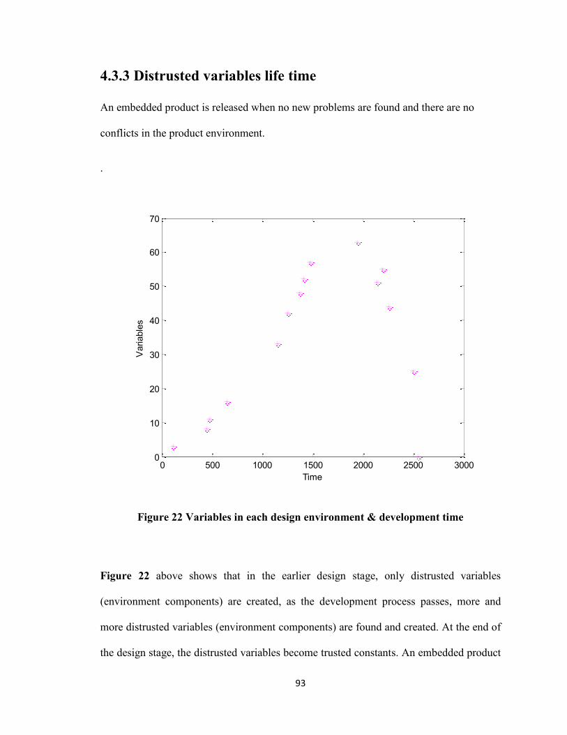
93
4.3.3 Distrusted variables life time
An embedded product is released when no new problems are found and there are no
conflicts in the product environment.
.
Figure 22 Variables in each design environment & development time
Figure 22 above shows that in the earlier design stage, only distrusted variables
(environment components) are created, as the development process passes, more and
more distrusted variables (environment components) are found and created. At the end of
the design stage, the distrusted variables become trusted constants. An embedded product
0 500 1000 1500 2000 2500 30000
10
20
30
40
50
60
70
Time
Variables
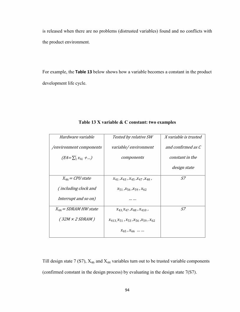
94
is released when there are no problems (distrusted variables) found and no conflicts with
the product environment.
For example, the Table 13 below shows how a variable becomes a constant in the product
development life cycle.
Table 13 X variable & C constant: two examples
Hardware variable
/environment components
(E4= 𝑥4𝑖 𝑖1 +…)
Tested by relative SW
variable/ environment
components
X variable is trusted
and confirmed as C
constant in the
design state
𝑋46= CPU state
( including clock and
Interrupt and so on)
𝑥41 ,𝑥43 ,𝑥45 ,𝑥47 ,𝑥48 ,
𝑥51 ,𝑥56 ,𝑥59 , 𝑥62
… …
S7
𝑋44= SDRAM HW state
( 32M × 2 SDRAM )
𝑥43,𝑥47 ,𝑥48 ,𝑥410 ,
𝑥413,𝑥51 ,𝑥53 ,𝑥56 ,𝑥59 , 𝑥62
𝑥65 ,𝑥66 … …
S7
Till design state 7 (S7), X46 and X44 variables turn out to be trusted variable components
(confirmed constant in the design process) by evaluating in the design state 7(S7).

95
4.3.4 EBD approach to the development process: examples
insert
Figure 23 EBD approach to the development process
In embedded system development engineering, developers very often rush to design HW or
start to write code without fully validating her/his thinking, even if she/he understands design
requirements rightly. Still, recommend that designers should validate his/her ideas before
taking a design action. Figure 23 above shows that those environment analysis activities are
inserted into some of the design process by evaluating, testing, investigating.

96
Those actions are in fact trying to investigate and find out:
a) Which are the distrusted variable /environment components in the design stage
b) Which are the trusted constant /environment components in a design stage
With environment analysis, some possible situations would be found in an earlier stage.
Examples are as follows:
Test designer’s thinking or idea before taking a design action. This is a human
environment analysis example.
Hidden problems such as electrical wiring problems: memory pins short or open, or
improperly inserted chips. Test if each of the address pins can be set to 0 and 1 without
affecting any of the others. This may be very helpful when developing a board support
package (BSP). This is a built environment analysis example.
4.3.5 Result of EBD approach
Table 14 Result with EBD
Design activity Design tasks Total
duration
(hours)
Rate
Design requirements
meeting, test/environment analysis, and
documentation
1,2,4,9,11,14,16,17,18
,
20,21,22,23,26,27,28,
31,33,34,36,49
860 33.81%
Detail DEV+ TEST( HW & SW ) 3,5,6,7,8,10,12,13,19,
24,25,29,30,32,35,41,
42,46
1436
56.45%
Final debugging verification, validation,
test and evaluation
and so on
37,38,39,40,43,44,45,
47,48
248
9.74%
Total 2544 100%

97
4.4 Quality of two approaches
In terms of development time, from the result with EBD (Table 14) and the result
without EBD (Table 9), we have the following comparing result shown in Figure 24
with two different development processes:
Product-based or process-based embedded system development process
Environment-based embedded system development
Figure 24 Quality of two approaches
0
500
1000
1500
2000
2500
3000
With EBD Without EBD
Final debugging verification ,validation , testand evaluationand so on
Detail DEV+ TEST( HW & SW )
Design requirements and documentation

98
Chapter 5
CONCLUSIONS AND FUTURE
WORK
In the present thesis, a new approach to embedded system design is introduced, its
application to embedded design is shown, and is a validated EBD using design log.
5.1 Conclusion: why use an EBD in embedded
system design
To sum up the case study from Chapter 3 and Chapter 4, the use of EBD in embedded
system design is recommended for the following reasons:
(1) Start to develop/code/design too early without completely understanding what to do, what
should be done, and how to do it, particularly in product life cycle thinking; This may
cause more time to redesign or debug
(2) Trying to fully understand the design requirements is the first thing an embedded
developer should do. Environment analysis in embedded system design includes :
a) Fully understand design requirements
b) Distinguish distrusted variables, and confirmed/ trusted constant component.
Distrusted variables in a design environment state example are the follow: unknown

99
SDRAM pins situation (pin open or short); Invalid/ bad block in a NAND flash
loading address.
Confirmed/ trusted constant environment component: tested SDRAM situation and
NAND flash loading address.
(3) The order of solving a problem is always to start from root conflicts. This is a question of
how to ask questions. Mostly, when a root conflict is solved, its relative dependent
conflicts would be solved or would be easier to be solved.
(4) Atomic design should be atomically developed. Once an atomic design problem is there
and it must be solved, the developer should persist and not move on to other tasks;
(5) Hidden conflicts can be found at an earlier stage by validating.
The hidden conflicts should not be found at the last moment;
(6) From the author's experience, without EBD, once a problem is too hard to be solved, he
would often easily:
a) Give up solving the current problem-A and then move on to solve problem-B.
Sometimes, a developer should not bypass the atomic design problem or a root
conflict and develop other tasks. Some tasks such as root conflicts should be
atomically finished;
b) Give up on solving current problem-A or generating solution-A and would then seek a
second solution such as solution-B. Sometimes solution-A may be related to a root
conflict and need to be solved before the generation of other solutions.
(7) In an embedded system development process, the environment analysis would depend on
the testing of some possible situation such as validating the designer’s thinking,

100
investigating a hidden problem, evaluating thinking and so on. For example, it may require
adding your relocation code into a good loader to see if it works. This is to evaluate if the
relocation code really works.
5.2 Future work
The following lists some points that we may require work in the future:
(1) About EBD
a) Environment analysis: ROM software should be developed more effectively
b) Conflict analysis and solution generation: more rules should be worked out.
(2) About the validation of EBD
a) More embedded system development should be carried out to validate EBD.
b) Design log is recommended to validate EBD.

101
APPENDIX
1.1 Overview of environment-based design
Environment-based design (EBD) is a design methodology derived from the axiomatic
theory of design modeling [40, 41]. Unlike the traditional design methodologies, the
EBD is based on the recursive logic of design. It provides guidance for designers from
the collection of necessary and sufficient information for a design task throughout the
generation and evaluation of design solutions.
The EBD includes three basic activities: environment analysis, conflict identification,
and solution generation. These three activities are interdependent and they work together
to generate and refine the design specifications and design solutions. In the following
sections, the recursive object model (ROM), a part of the EBD theory, will be first
introduced [40, 42, 43]. This is followed by the discussion of the three basic activities
sequentially.
1.2 Recursive object model

102
1.2.1 Mathematical foundation
The axiomatic theory of design modeling is a logical tool used to represent and reason
about object structures [41]. It is a formal approach for the development of design
theories following logical steps based on mathematical concepts and axioms. The basic
concepts of the universe and object and relation relies on two axioms: (1) Everything in
the universe is an object; (2) There are relationships between objects.
On the basis of the axiomatic theory of design modeling, structure operation is
developed to model the structure of complex objects. Structure operation ( ) is defined
by the union ( ) of an object and the interaction ( ) of the object with itself [41].
Where O is the structure of an object O, everything in the universe can be viewed as
an object. Interactions between objects are also objects. Hence, structure operation
allows us to represent a hierarchical system with a single mathematical expression.
Suppose an object O is composed of m sub objects Oi (i=1, 2, …, m). O can be
represented as follows:
where m is a finite natural number. Based on Eqs. (1) and (2), the structure of the object
O can be expanded as:

103
The above equations imply a recursive representation of an object.
Due to the capacity of human cognition and the scope of applications, the idea of a
primitive object is introduced. A primitive object, denoted by a
iO, is an object that
cannot or need not be further decomposed.
The object O may include other objects, suggesting that Eq. (1) is a recursive
representation of an object.
1.2.2 ROM: graphical representation of a natural language
The recursive object model (ROM) is a part of the EBD theory. It is a simple graphic
language used as an intermediate medium between natural language and structured
modeling language [40, 42, 43]. As shown in Table 1, the ROM is composed of five
basic elements, including two kinds of objects and three kinds of relationships [42].

104
Table 1 Symbols used in ROM[42].
Constraints ( ), represented by an arrow with a dotted head in Table 1, is a descriptive,
limiting, or particularizing relation of one object to another. The arrow for the symbol
representing constraints always points to the object to be constrained. A constraint
relation can be considered as an interaction from the constraining object Oi to the
constrained object Oj.
Connection relation ( ) is defined as the connection of two objects that do not constrain
each other. It can be considered as the interaction of one object Oi with another object
Oj.

105
Predicate relation ( ) is the relation representing an act of an object on another or
representing the state of an object. It can be view as the interaction of one object Oi with
another object Oj.
Based on the ROM theory, each paragraph is composed of sentences. Each sentence
consists of phrases. Each phrase can be decomposed into words, which can be taken as
the primitive objects. Paragraphs, sentences and phrases are compound objects. The
ROM theory says that each word in a sentence is an object and each object may have
one or more relations to other objects. Furthermore, each sentence is also an object and
has a relation to other sentences in the paragraph.
1.2.3 ROMA: translation of natural language to ROM diagram
The ROM has been shown to be useful and applicable to many different problems.
Based on the ROM theory, a software system, ROMA, has been developed to support
the transformation of natural language into ROM diagrams[42]. The input of the ROMA
system is a paragraph of text and the output is the corresponding ROM diagrams. Most
of grammatically correct complex and simple sentences can be handled by the software.
The user interface feature of the software system allows users to interact with the
generated ROM diagrams and thus any problems produced during the transformation
process can be corrected in a user-friendly manner. This software allows designers to
generate ROM diagram much faster and therefore saves time in the design process.

106
1.3 Formulization of design requirements
As shown previously, the ROM diagram is a graphic representation of natural language.
The ROM has been proposed as a general methodology for the process of formalizing
design requirements [40, 42]. Based on the foundation of ROM theory, a product system
can be defined as the structure of an object ( ) which includes a product (S) and its
environment (E)[40]. The product can be a software package, a process, an idea and so
on. Except for the product itself, everything else can be considered as an environment,
which can be direct, close and remote[44]. According to the properties, the environment
can also be divided into three kinds: natural, built, and human[40] .Built environments
are the artifacts designed and created by human beings whereas the human environment
includes all of the human beings but particularly the human users of an artifact.
where is the object that is included in any object.
On the basis of the structure operation defined in Eqs. (1)-(3), the product system can be
expressed as follows:
where E and S are structures of the environment and product, respectively. E S
and SE are the interactions between the environment and product.
Figure 1 shows the product system[40]. Since both the environment and the product may
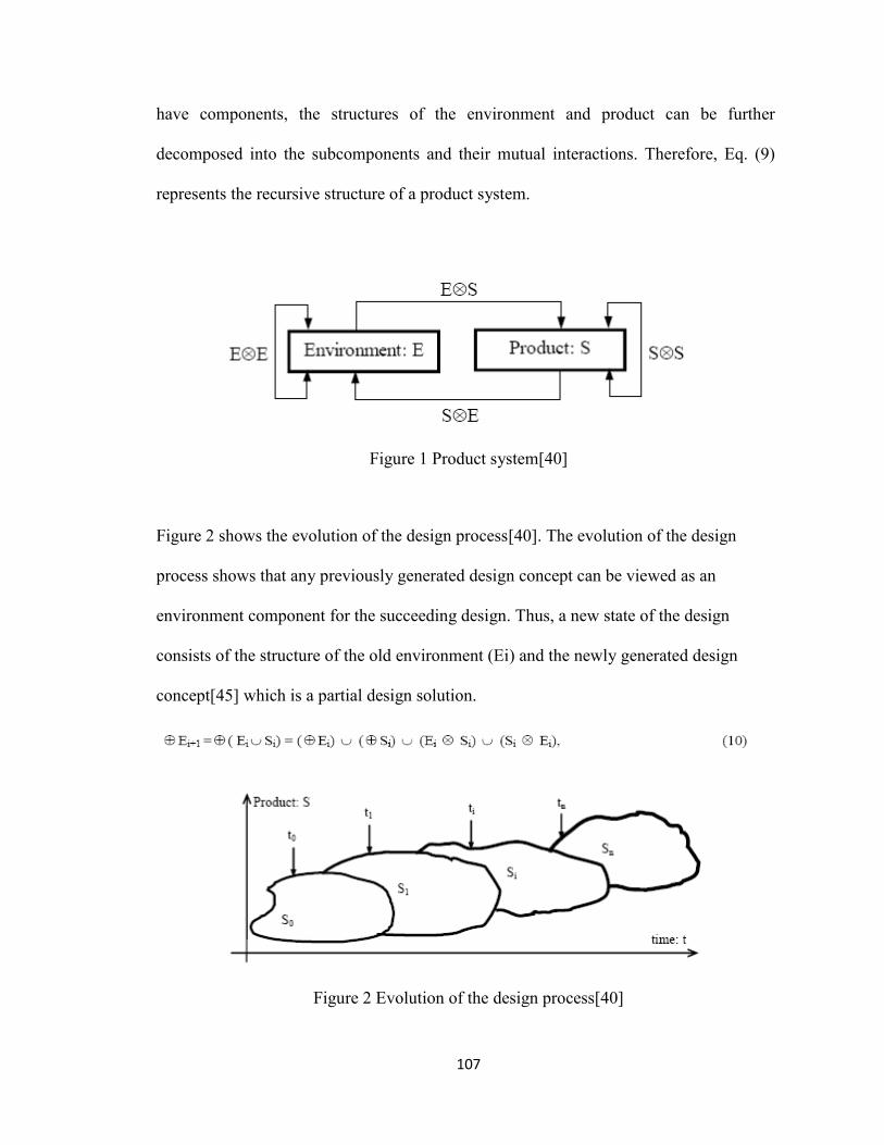
107
have components, the structures of the environment and product can be further
decomposed into the subcomponents and their mutual interactions. Therefore, Eq. (9)
represents the recursive structure of a product system.
Figure 1 Product system[40]
Figure 2 shows the evolution of the design process[40]. The evolution of the design
process shows that any previously generated design concept can be viewed as an
environment component for the succeeding design. Thus, a new state of the design
consists of the structure of the old environment (Ei) and the newly generated design
concept[45] which is a partial design solution.
Figure 2 Evolution of the design process[40]

108
The recursive logic of design indicates that during the design process design knowledge
provides the basis for the generation and evaluation of design solutions and that the
design knowledge used for the current design is determined by the design solutions.
The formula of the engineering system can be derived from the natural language
requirement using ROM. The formulization process for the design requirements is
shown in Figure 3[43].
Figure 3 Formulization process of design requirements[43]

109
1.4 Environment analysis
The objective of environment analysis is to find out the key environment components, in
which the desired product works, and the relationships between the environment
components. The environment can be divided into natural, built and human based on the
properties or divided into close and remote based on their importance for the product
[40]. From the environment implied in the design problem described by the customers,
the designer will introduce extra environment components that are relevant to the design
problem at hands. The results from this analysis constitute an environment analysis. One
of the key methods for environment analysis is linguistic analysis. There are two types
of questions to be asked in environment analysis. These questions are generated by
ROM.
The first types of questions to be asked is generic questions, which are used to help
designers better understand the design problem through the ROM linguistic analysis. As
shown in Figure 4, each object in a ROM diagram is analyzed as a center object or a
constraining object which will be further identified or clarified.

110
Figure 4 Asking the generic questions[46]
Table 2.2 gives two rules for asking a question. These rules can be applied to determine
which objects should be extended first.
Table 2 Rules for generic questions [46]
Rule 1 Before an object can be further defined, the objects constraining them
should be defined.
Rule 2 An object with the most undefined constraints should be considered first.

111
The second type of questions is the domain specific questions. The main aim of domain
questions is to collect the information that would have a significant influence on the
design problem. The collected information consists of the domain-related environment
components, as well as their relationships that are defined without the knowledge about
design requirements and final solutions. Table 3 shows rules for asking domain-specific
questions and Figure 5 shows the main procedure for asking domain specific questions.
Table 3 Rules for asking domain-specific questions[46]
Rule 3 First to ask: what is the life cycle of the product to be designed?
Rule4 Ask questions about the natural, built, and human environment about each
state of the lifecycle of the product.
Rule 5 The sequence for asking questions is determined by the levels of
requirements in the EBD process so that those requirements at the lower
levels have higher priority and can be asked earlier.
Rule 6 Ask questions about the answers from Rule 1 and Rule 2 by applying the
rules related to generate generic questions.

112
Figure 5 Ask domain-specific questions [46]
1.5 Conflict identification
Conflict identification aims at identifying undesired conflicts between environment
relationships. A conflict consists of three elements: two competing objects and one
resource object which the former two objects contend for [47] . Conflicts are viewed as
the driving force in the EBD process. Table 4 shows three rules for the identification of
potential conflicts from a ROM diagram. These rules are not inclusive and are complete.
More robust rules need to be developed.

113
Table 4 Rules for identifying potential conflicts[12]
Rule 1 If an object has multiple constraints, then potential conflict exists between
any pair of constraining objects.
Rule 2 If an object has multiple predicate relations from other objects, then
potential conflict exists between a pair of those predicate relations.
Rule 3 If an object has multiple predicate relations to other objects, then a
potential conflict exists between a pair of those predicate relations.
1.6 Solution generation
The main goal of the design solutions is to meet the requirements. By generating some
design solutions, a set of key environment conflicts will be chosen and resolved at this
step. The newly generated solution becomes a part of the new product environment for
the succeeding design. This process continues until no more undesired environment
conflicts exist.
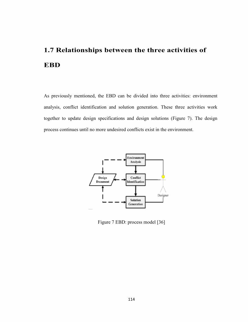
114
1.7 Relationships between the three activities of
EBD
As previously mentioned, the EBD can be divided into three activities: environment
analysis, conflict identification and solution generation. These three activities work
together to update design specifications and design solutions (Figure 7). The design
process continues until no more undesired conflicts exist in the environment.
Figure 7 EBD: process model [36]

115
Bibliography
1. Marwedel, P., Embedded system design, 2006, Springer: The Netherlands. p. 1-
12.
2. Akin, Ö. and C. Akin, On the process of creativity in puzzles, inventions, and
designs. Automation in Construction, 1998. 7(2-3): p. 123-138.
3. Wikipedia Schematic http://en.wikipedia.org/wiki/Schematic 2011.
4. Wikipedia Printed circuit board
http://en.wikipedia.org/wiki/Printed_circuit_board. 2011.
5. Dubey, R., Introduction to embedded system design using field programmable
gate arrays, 2009, Springer: London. p. 1-16.
6. Coombs, C.F., Printed circuits handbook. 6th ed ed2008, New York: McGraw-
Hill.
7. Wikipedia, Boot loader http://en.wikipedia.org/wiki/Booting. 2011.
8. Wikipedia, kernel http://en.wikipedia.org/wiki/Kernel_%28computing%29. 2011.
9. Wikipedia, device driver http://en.wikipedia.org/wiki/Device_driver. 2011.
10. Wikipedia, Root File System http://en.wikipedia.org/wiki/File_system. 2011.
11. Wikipedia, application http://en.wikipedia.org/wiki/Application_software. 2011.
12. Zeng, Y. Environment-based design (EBD). in the ASME 2011 International
Design Engineering Technical Conferences & computers and Information in
Engineering Conference. 2011. Washinton, DC, USA.
13. Peter, K., Design methodology and the nature of technical artefacts. Design
Studies, 2002. 23(3): p. 287-302.

116
14. Jones, J.C., and D.G. Thornley, ed. Conference on design methods. 1963,
Pergamon Press: Oxford.
15. Cross, N., Science and design methodology: a review. Research in Engineering
Design, 1993. 5: p. 63-69.
16. Dowty, M., Test Driven Development of Embedded Systems Using Existing
Software Test Infrastructure, in In Colorado Undergraduate Space Research
Symposium2004: University of Colorado at Boulder.
17. Altizer, B. and B. Consulting Toward A Methodology For Platform-Based Design
of Embedded Systems
http://www.basysconsulting.com/BASYSPubs/BASYS_PBD_White_Paper.pdf.
2002.
18. L.P, B. Businessweek "Inside Intel" January 9,2006.
19. Sangiovanni-Vincentelli, A. and G. Martin, Platform-based design and software
design methodology for embedded systems. Design & Test of Computers, IEEE,
2001. 18(6): p. 23-33.
20. Keutzer, K., et al., System-level design: orthogonalization of concerns and
platform-based design. Computer-Aided Design of Integrated Circuits and
Systems, IEEE Transactions on, 2000. 19(12): p. 1523-1543.
21. Sander, I. Platform-Based Design of Heterogeneous Embedded Systems
http://www.snart.org/docs/2009/Ingo_handouts_RTiS2009.pdf. Aug,19,2009.
22. Camposano, R. and J. Wilberg, Embedded system design. Design Automation for
Embedded Systems, 1996. 1(1): p. 5-50.
117
23. De Michell, G. and R.K. Gupta, Hardware/software co-design. Proceedings of the
IEEE, 1997. 85(3): p. 349-365.
24. Ernst, R., J. Henkel. Hardware-software co-design of embedded controllers based
on hardware extraction. in Handouts of the workshop on Hardware-Software Co-
Design. 1992.
25. Adams, K., H. Schmitt, and D. Thomas. A model and methodology for hardware-
software codesign. in International Workshop on Hardware-Software Codesign
1993. Cambridge, Massaschusetts.
26. Wolf, W.H., Hardware-software codesign of embedded systems. Proceedings of
the IEEE, 1994. 82(7): p. 967-998.
27. Abid, M., T.B. Ismail, A. Changuel, C.A. Valderrama, M. Romdhani, G.F.
Marchioro, J.M. Daveau, and A.A. Jerraya, Hardware/software co-design
methodology for design of embedded systems. Integrated Computer-Aided
Engineering, 1998. 5(1): p. 69-83.
28. Wolf, P.v.d., et al., Design and programming of embedded multiprocessors: an
interface-centric approach, in Proceedings of the 2nd IEEE/ACM/IFIP
international conference on Hardware/software codesign and system
synthesis2004, ACM: Stockholm, Sweden. p. 206-217.
29. Alfaro, L.d. and T.A. Henzinger, Interface Theories for Component-Based
Design, in Proceedings of the First International Workshop on Embedded
Software2001, Springer-Verlag. p. 148-165.
30. Nicolescu, G., P.J. Mosterman, Model-based design for embedded systems2010,
Boca Raton, FL: CRC Press.

118
31. Schattkowsky, T., W. Muller, Model-based design of embedded systems.
Proceedings of the Seventh IEEE International Symposium on Object-Oriented
Real-Time Distributed Computing, 2004.
32. Daniel D. Gajski , S.A., Andreas Gerstlauer , Gunar Schirner, Embedded system
design2009, Irvine, CA ,U.S.A & Austin, TX, U.S.A: Springer Dordrecht
Heidelberg London New York. 352.
33. Sangiovanni-Vincentelli, A., M. Sgroi and L. Lavagno,, Formal models for
communication based design.
34. Kienhuis, B., E. Deprettere, K. Vissers, and P. van der Wolf. An approach for
quantitative analysis of application-specific dataflow architectures. in
Proceedings of Eleventh International conference of applications-specific
systems, Architectures and Processors (ASAP’97). 1997. Zurich, Switzerland.
35. Kienhuis, B., E.F. Deprettere, P. van de Wolf, and K. Vissers, A methodology to
design programmable embedded systems-The Y-char approach. Embedded
Processor Design challengers: Systems, Architectures, Modeling, and Simulation-
SAMOS 2002: p. 18-37.
36. Chen, M., Chen, Z., Kong, L., Zeng, Y., Analysis of medical devices design
requirements. Journal of Integrated Design and Process Science, 2005: p. 61-70.
37. Chen, Z.Y., Zeng, Y., Classification of product requirements based on product
environment. Concurrent Engineering, 2006. 14(3): p. 219-230.
38. Standish, http://www.it-cortex.com/Stat_Failure_Rate.htm, 1995
39. Wang, M. and Y. Zeng, Asking the right questions to elicit product requirements.
Int. J. Comput. Integr. Manuf., 2009. 22(4): p. 283-298.
119
40. Zeng, Y., Environment-based formulation of design problem. Transaction of
SDPS: Journal of Integrated Design and Process Science, 2004. 8(4): p. 45-63.
41. Zeng, Y., Axiomatic theory of design modeling. Transaction of SDPS: Journal of
Integrated Design and Process Science, 2002. 6(3): p. 1-28.
42. Zeng, Y., Recursive object model (ROM)-modeling of linguistic information in
engineering design. Computers in Industry, 2008. 59(6): p. 612-625.
43. Zeng, Y., Formalization of design requirements. in: Integrated Design of Process
Technologies (IDPT-2003), 2003.
44. Hubka, V.a.E., W.E, Theory of technical systems: A total concept theory for
engineering design1988: Spring-Verlag.
45. Blessing, L.T.S., Chakrabarti, A., DRM, a Design Research Methodology2009,
London: Springer.
46. Wang, M., Zeng, Y., Asking the right questions to elicit product requirements.
International Journal of Computer Integrated Manufacturing, 2009. 22(4): p. 283-
298.
47. Yan, B., Zeng, Y. On the structure of design conflicts. in The 12th World
Conference on Integrated Design & Process Technology. 2009. Alabama, USA.