Embed Size (px)
Citation preview

An alternative route towards micro- and nano-patterning of oxide films
This article has been downloaded from IOPscience. Please scroll down to see the full text article.
2012 Nanotechnology 23 085302
(http://iopscience.iop.org/0957-4484/23/8/085302)
Download details:
IP Address: 192.108.69.177
The article was downloaded on 19/03/2012 at 10:51
Please note that terms and conditions apply.
View the table of contents for this issue, or go to the journal homepage for more
Home Search Collections Journals About Contact us My IOPscience
IOP PUBLISHING NANOTECHNOLOGY
Nanotechnology 23 (2012) 085302 (7pp) doi:10.1088/0957-4484/23/8/085302
An alternative route towards micro- andnano-patterning of oxide filmsG Bridoux1, J Barzola-Quiquia1, F Bern1, W Bohlmann1, I Vrejoiu2,M Ziese1 and P Esquinazi1
1 Division of Superconductivity and Magnetism, University of Leipzig, Linnestrasse 5, D-04103 Leipzig,Germany2 Max-Planck-Institut fur Mikrostrukturphysik, D-06120 Halle, Germany
E-mail: [email protected] and [email protected]
Received 9 September 2011, in final form 12 January 2012Published 1 February 2012Online at stacks.iop.org/Nano/23/085302
AbstractThis paper presents a method to obtain submicron- and nanometer structures of different oxidefilms and heterostructures combining e-beam lithography and chemical etching. The mostrelevant advantage of this method is that structures of tens of microns in length and below∼100 nm width can be produced, keeping the intrinsic bulk film properties, as proven byelectrical transport measurements. In this way our method provides a bridge that connects theattractive properties of oxide films and the nanoworld.
(Some figures may appear in colour only in the online journal)
1. Introduction
The development of oxide materials has been one of theimportant engines in solid state physics during the lastdecades. From semiconducting [1], superconducting [2] toferromagnetic and ferroelectric oxides [3], all the maincondensed matter fields were boosted by these compounds.On the other hand, a broad application of oxide thin films andmultilayers within nanotechnology still remains a challenge.Thin films play a key role in the development of thesedevices. Therefore, it is extremely important to have asimple, inexpensive and reliable method to build micron-,submicron- and nanostructures of different oxide films. Theaim of this work is to present a method that combineslithography and chemical etching to obtain submicron- andnanopatterns in different oxide films and heterostructures. Inparticular we have used electron-beam (e-beam) lithographydue to the flexibility in the final patterns that can be drawnin the electron-beam resist: however, similar results can beachieved using other lithography techniques.
Many efforts for micro- and nano-patterning of oxidefilms have been made in recent years. One possibility is theuse of in situ nano-patterning during the oxide film growthbut this possibility has not materialized yet. A combinationof e-beam lithography and ion-beam etching is the optionthat many groups have chosen nowadays [4–6]. However,the drawback of this method is the ion contamination that
the thin film suffers during patterning, losing in this way itsintrinsic properties. We describe here an experimental methodthat combines e-beam lithography with wet chemical etching,allowing us to create micron-, submicron- and nanostructuresin different oxide films such as La1−xCaxMnO3 (LCMO),La1−xSrxMnO3 (LSMO), YBa2Cu3O7−δ (YBCO), ZnO,Fe3O4 and PbZr1−xTixO3 (PZT) avoiding any contamination.Other groups have tried a similar approach in some of theabove-mentioned compounds [7–10]. However, in contrastto those works, our method allows us to study oxidematerials at micron-, submicron- and nanometer length scaleswith well-defined cross sections and small roughness, asdemonstrated in the following sections. As an example, insection 4 of this paper the evolution of the electric transportproperties of ferromagnetic metallic La0.7Sr0.3MnO3 isdescribed as a function of wire width from ∼100 µm downto ∼0.1 µm.
2. Experimental details
The first step is to check if the e-beam resist (PMMA 950K,AR-P 671-05) layer remains intact after the immersion in thecorresponding acid solution that will constitute the etchant forthe particular oxide material. This procedure has been checkedsuccessfully for all the acid solutions investigated, see table 1.
After this, an e-beam writes an arbitrary pattern on theresist that covers the oxide film. The parts of the PMMA
10957-4484/12/085302+07$33.00 c© 2012 IOP Publishing Ltd Printed in the UK & the USA
Nanotechnology 23 (2012) 085302 G Bridoux et al
Table 1. Some of the oxide film materials used in this work to produce micro- and nanostructures and the corresponding acid solutions andetching rates. The expected chemical reactions are listed in the appendix.
Oxide film Oxide bilayer or multilayer Acid solutionEtching rate(nm s−1)
La0.7Ca0.3MnO3 4 ml HCl 35 wt%+4 ml KI 3 M in H2O+ 70 ml H2O
∼35
La0.7Sr0.3MnO3
ZnO 50 ml H3PO4 85 wt% in H2O+ 50 ml H2O ∼60Zn1−xCoxOZn1−xMnxOZn1−xMgxO
YBa2Cu3O7 1 g (2.53 mmol)C10H14N2Na3O8.2H2O+ 70 ml H2O at 80 ◦C
∼50
GdBa2Cu3O7PrBa2Cu3O7
Fe3O4 5 ml HCl 35 wt% in H2O+ 20 ml HF 48 wt% inH2O+ 70 ml H2O at 70 ◦C
∼200
Fe2O3ZnFe2O4
La0.7Sr0.3MnO3/PbZr0.2Ti0.8O3 60 ml HCl 35 wt% in H2O+ 4 ml KI 3 M inH2O+ 900 ml H2O+ 6 ml 7:1 NH4F:HF(0.85 ml 48% HF, 0.19 g of NH4F in 5.15 ml ofH2O = 5.15 mmol) + 60 ml aceticacid+ 60 ml HNO3 + 16 g (0.04 mol) EDTAtrisodium+ 40 g (0.75 mol) NH4Cl
∼1
exposed to the e-beam are removed using the correspondingdeveloper (AR 600-55). The regions of the film covered bythis resist will be protected from the acid solution, whilethe rest of the film will be removed after immersion in thecorresponding acid solution, as can be seen in the images offigures 1(a) and (b). Following this procedure and tuning thesolution concentration and the etching rate for each oxide film(see table 1), a controlled design of micro- and nano-patternscan be achieved, see the images in figures 1(c)–(e). Table 1summarizes the most concentrated solutions we have used(with the higher etching rates). However, we have checkedthat the dilution of these ones leads to lower etching rateswithout degradation of the nanostructural features. A linearrelation between the total thickness of the oxide film (rangingfrom 20 to 500 nm) and the total immersion time in itscorresponding acid solution has also been proved. It isalso important to note that, in all the fabricated submicronstructures, the total etching time for a particular etchingsolution is always much less than the time required toproduce an etching of the oxide substrate. This was verifiedby immersing different substrates (SrTiO3, Al2O3, etc) witha patterned PMMA on top in the etching solutions listedin table 1 during several minutes, resulting in unchangedsurfaces.
3. Results and discussion
3.1. General characteristics of the patterned structures
The AFM and SEM images of figures 2 and 3 show some ofthe main features of the structures. In figure 2, AFM images
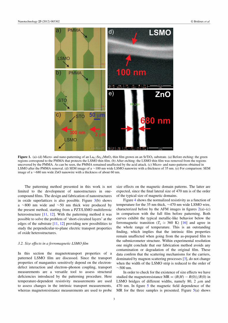
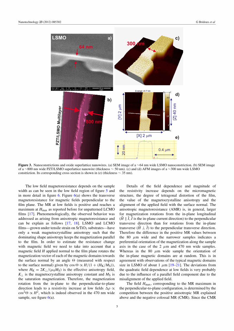
show an LSMO structure varying in width continuously fromseveral tens of microns down to∼470 nm. Figures 3(a) and (c)present AFM images of LSMO nanoconstrictions of ∼64 nmand ∼300 nm width, respectively. Relevant characteristics ofthe fabricated structures are the sharpness of the edges, thewell-defined cross section, see figures 2 and 3(e), the smallroughness and the large extension along one direction, as canbe noticed in figure 2.
The cross-section profiles of figures 2 and 3(e) show asloping angle α ∼ 35 ◦C, a feature that is present in all thefabricated nanostructures. Hence, for a fixed patterned widthon the PMMA (minimum width ≤ 100 nm), wPMMA, theresulting width of the oxide film, w, is approximately equalto the difference between wPMMA and 2t tan(α), where t isthe total thickness of the oxide film. We have experimentallyverified this relation for all the oxide films listed in table 1(with thicknesses from 20 to 500 nm) with their correspondingchemical etchant (also listed in table 1). On the other hand, ifthe etching process is isotropic α ∼ 45 ◦C. However, in ournanostructures it seems that the etching rate in the verticaldirection (listed in table 1) is ∼cot 35◦ = 1.43 times largerthan in the horizontal direction. Our starting oxide thin filmswere mainly grown by pulsed laser deposition (PLD) andpost-annealed in oxygen atmosphere above 300 ◦C in mostof the cases, resulting in epitaxial or textured films with ahigh crystalline anisotropy [11–15] that is reflected in theirphysical and chemical properties. Hence we do not discardthe possibility that the chemical solutions listed in table 1 etchin a preferential crystalline direction of our oxide thin films.A detailed explanation of this mechanism is beyond the scopeof this work.
2
Nanotechnology 23 (2012) 085302 G Bridoux et al
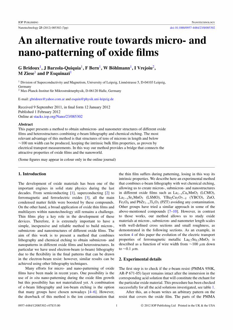
Figure 1. (a)–(d) Micro- and nano-patterning of an La0.7Sr0.3MnO3 thin film grown on an SrTiO3 substrate. (a) Before etching: the greenregions correspond to the PMMA that protects the LSMO thin film. (b) After etching: the LSMO thin film was removed from the regionsuncovered by the PMMA. As can be seen, the PMMA remained unaffected by the acid attack. (c) Micro- and nano-patterns obtained inLSMO after the PMMA removal. (d) SEM image of a ∼100 nm wide LSMO nanowire with a thickness of 35 nm. (e) For comparison: SEMimage of a ∼680 nm wide ZnO nanowire with a thickness of about 60 nm.
The patterning method presented in this work is notlimited to the development of nanostructures in one-compound films. The design and fabrication of nanostructuresin oxide superlattices is also possible. Figure 3(b) showsa ∼800 nm wide and ∼50 nm thick wire produced bythe present method, starting from a PZT/LSMO multiferroicheterostructure [11, 12]. With the patterning method it waspossible to solve the problem of ‘short-circuited layers’ at theedges of the substrate [11, 12] providing new possibilities tostudy the perpendicular-to-plane electric transport propertiesof oxide heterostructures.
3.2. Size effects in a ferromagnetic LSMO film
In this section the magnetotransport properties of apatterned LSMO film are discussed. Since the transportproperties of manganites sensitively depend on the electron-defect interaction and electron–phonon coupling, transportmeasurements are a versatile tool to assess structuraldeficiencies introduced by the patterning procedure. Heretemperature-dependent resistivity measurements are usedto assess changes in the intrinsic transport measurements,whereas magnetoresistance measurements are used to probe
size effects on the magnetic domain patterns. The latter areexpected, since the final lateral size of 470 nm is of the orderof the typical size of magnetic domains.
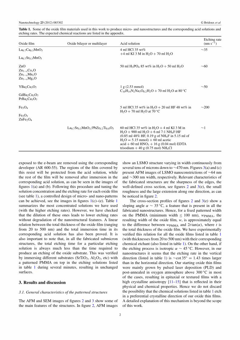
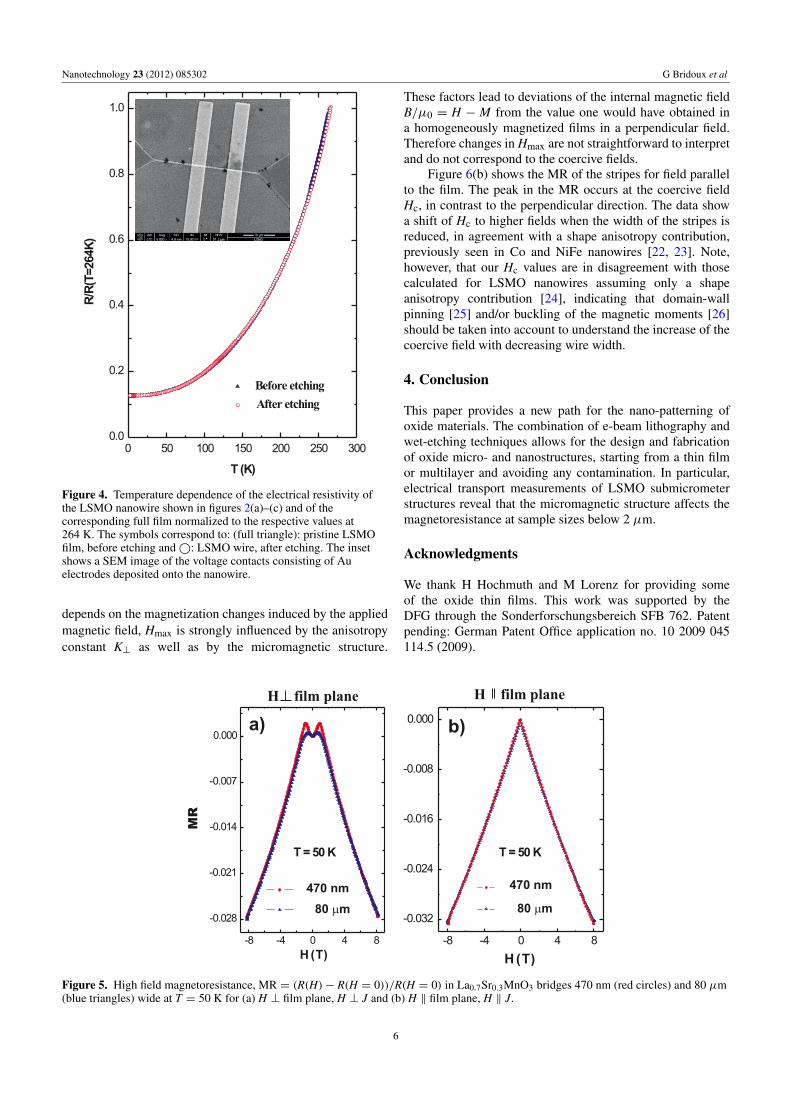
Figure 4 shows the normalized resistivity as a function oftemperature for the 35 nm thick, ∼470 nm wide LSMO wire,characterized before by the AFM images in figures 2(a)–(c)in comparison with the full film before patterning. Bothcurves exhibit the typical metallic-like behavior below theferromagnetic transition (Tc ' 360 K) [16] and agree inthe whole range of temperature. This is an outstandingfinding, which implies that the intrinsic film propertiesremain unaffected when going from the as-prepared film tothe submicrometer structure. Within experimental resolutionone might conclude that our fabrication method avoids anycontamination or degradation of the original film. Thesedata confirm that the scattering mechanisms for the carriers,dominated by magnon scattering processes [3], do not changewhen the width of the LSMO strip is reduced to the order of∼500 nm.
In order to check for the existence of size effects we havestudied the magnetoresistance MR = (R(H) − R(0))/R(0) inLSMO bridges of different widths, namely 80, 2 µm and470 nm. In figure 5 the magnetic field dependence of theMR for the three samples is presented. Figure 5(a) shows
3
Nanotechnology 23 (2012) 085302 G Bridoux et al
Figure 2. AFM images of a continuous LSMO structure varying in width from several tens of microns down to ∼470 nm. The bottom traceshows a cross section of the nanostructure (thickness ∼ 35 nm). From this trace one can estimate that the sloping angle is at least 35 ◦C, alower limit set by the rounding of the AFM tip.
the corresponding data for magnetic fields H perpendicularto the film plane and perpendicular to the electrical currentdensity J, whereas figure 5(b) shows the in-plane MR datafor the magnetic field parallel to the current density. In both
field orientations the high field magnetoresistance is negativeand does not depend on the width of the LSMO bridge, inagreement with the results of figure 4, showing again that theintrinsic transport properties are not affected by the patterning.
4
Nanotechnology 23 (2012) 085302 G Bridoux et al
Figure 3. Nanoconstrictions and oxide superlattice nanowires. (a) SEM image of a ∼64 nm wide LSMO nanoconstriction. (b) SEM imageof a ∼800 nm wide PZT/LSMO superlattice nanowire (thickness ∼ 50 nm). (c) and (d) AFM images of a ∼300 nm wide LSMOconstriction. Its corresponding cross section is shown in (e) (thickness ∼ 35 nm).
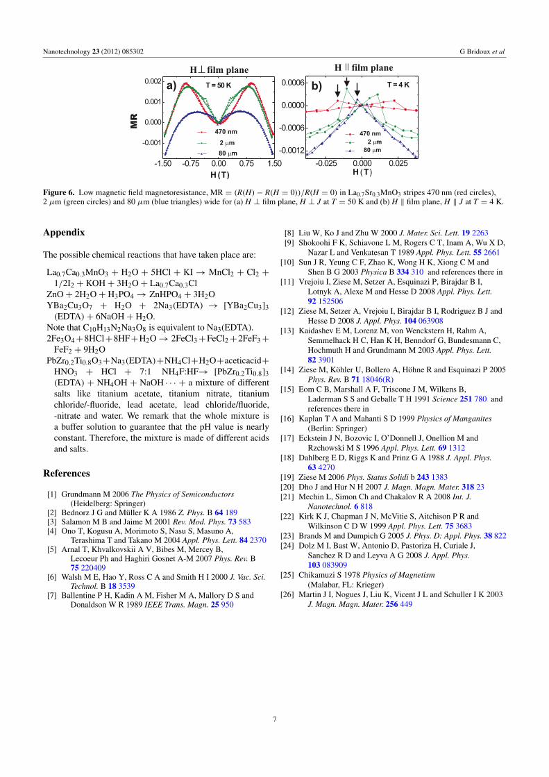
The low field magnetoresistance depends on the samplewidth as can be seen in the low field region of figure 5 andin more detail in figure 6. Figure 6(a) shows the transversemagnetoresistance for magnetic fields perpendicular to thefilm plane. The MR at low fields is positive and reaches amaximum at Hmax as reported before for unpatterned LCMOfilms [17]. Phenomenologically, the observed behavior wasaddressed as arising from anisotropic magnetoresistance andcan be explain as follows [17, 18]. LSMO and LCMOfilms—grown under tensile strain on SrTiO3 substrates—haveonly a weak magnetocrystalline anisotropy such that thedominating shape anisotropy keeps the magnetization parallelto the film. In order to estimate the resistance changewith magnetic field we need to take into account that amagnetic field H applied normal to the film plane rotates themagnetization vector of each of the magnetic domains towardsthe surface normal by an angle 2 (measured with respectto the surface normal) given by cos2 ∝ H/(1 + (HK/MS)),where HK = 2K⊥/(µ0MS) is the effective anisotropy field,K⊥ is the magnetocrystalline anisotropy constant and MS isthe saturation magnetization. Therefore, the magnetizationrotation from the in-plane to the perpendicular-to-planedirection leads to a resistivity increase at low fields 1ρ ∝cos22 ∝ H2, which is indeed observed in the 470 nm widesample, see figure 6(a).
Details of the field dependence and magnitude ofthe resistivity increase depends on the micromagneticstructure, the degree of tetragonal distortion of the film,the value of the magnetocrystalline anisotropy and thealignment of the applied field with the surface normal. Theanisotropic magnetoresistance (AMR) is, in general, largerfor magnetization rotations from the in-plane longitudinal( EH ‖ I, I is the in-plane current direction) to the perpendiculartransverse direction than for rotations from the in-planetransverse ( EH ⊥ I) to the perpendicular transverse direction.Therefore the difference in the positive MR values betweenthe 80 µm wide and the narrower samples indicates apreferential orientation of the magnetization along the sampleaxis in the case of the 2 µm and 470 nm wide samples.Whereas in the 80 µm wide sample the orientation ofthe in-plane magnetic domains are at random. This is inagreement with observations of the typical magnetic domainssize in LSMO of about 1 µm [19–21]. The deviations fromthe quadratic field dependence at low fields is very probablydue to the influence of a parallel field component due to themisalignment of the applied field.
The field Hmax, corresponding to the MR maximum inthe perpendicular-to-plane configuration, is determined by thecompetition between the positive anisotropic MR explainedabove and the negative colossal MR (CMR). Since the CMR
5
Nanotechnology 23 (2012) 085302 G Bridoux et al
Figure 4. Temperature dependence of the electrical resistivity ofthe LSMO nanowire shown in figures 2(a)–(c) and of thecorresponding full film normalized to the respective values at264 K. The symbols correspond to: (full triangle): pristine LSMOfilm, before etching and©: LSMO wire, after etching. The insetshows a SEM image of the voltage contacts consisting of Auelectrodes deposited onto the nanowire.
depends on the magnetization changes induced by the appliedmagnetic field, Hmax is strongly influenced by the anisotropyconstant K⊥ as well as by the micromagnetic structure.
These factors lead to deviations of the internal magnetic fieldB/µ0 = H − M from the value one would have obtained ina homogeneously magnetized films in a perpendicular field.Therefore changes in Hmax are not straightforward to interpretand do not correspond to the coercive fields.
Figure 6(b) shows the MR of the stripes for field parallelto the film. The peak in the MR occurs at the coercive fieldHc, in contrast to the perpendicular direction. The data showa shift of Hc to higher fields when the width of the stripes isreduced, in agreement with a shape anisotropy contribution,previously seen in Co and NiFe nanowires [22, 23]. Note,however, that our Hc values are in disagreement with thosecalculated for LSMO nanowires assuming only a shapeanisotropy contribution [24], indicating that domain-wallpinning [25] and/or buckling of the magnetic moments [26]should be taken into account to understand the increase of thecoercive field with decreasing wire width.
4. Conclusion
This paper provides a new path for the nano-patterning ofoxide materials. The combination of e-beam lithography andwet-etching techniques allows for the design and fabricationof oxide micro- and nanostructures, starting from a thin filmor multilayer and avoiding any contamination. In particular,electrical transport measurements of LSMO submicrometerstructures reveal that the micromagnetic structure affects themagnetoresistance at sample sizes below 2 µm.
Acknowledgments
We thank H Hochmuth and M Lorenz for providing someof the oxide thin films. This work was supported by theDFG through the Sonderforschungsbereich SFB 762. Patentpending: German Patent Office application no. 10 2009 045114.5 (2009).
Figure 5. High field magnetoresistance, MR = (R(H)− R(H = 0))/R(H = 0) in La0.7Sr0.3MnO3 bridges 470 nm (red circles) and 80 µm(blue triangles) wide at T = 50 K for (a) H ⊥ film plane, H ⊥ J and (b) H ‖ film plane, H ‖ J.
6
Nanotechnology 23 (2012) 085302 G Bridoux et al
Figure 6. Low magnetic field magnetoresistance, MR = (R(H)− R(H = 0))/R(H = 0) in La0.7Sr0.3MnO3 stripes 470 nm (red circles),2 µm (green circles) and 80 µm (blue triangles) wide for (a) H ⊥ film plane, H ⊥ J at T = 50 K and (b) H ‖ film plane, H ‖ J at T = 4 K.
Appendix
The possible chemical reactions that have taken place are:
La0.7Ca0.3MnO3 + H2O + 5HCl + KI→ MnCl2 + Cl2 +1/2I2 + KOH+ 3H2O+ La0.7Ca0.3Cl
ZnO+ 2H2O+ H3PO4 → ZnHPO4 + 3H2OYBa2Cu3O7 + H2O + 2Na3(EDTA) → [YBa2Cu3]3(EDTA)+ 6NaOH+ H2O.
Note that C10H13N2Na3O8 is equivalent to Na3(EDTA).2Fe3O4+8HCl+8HF+H2O→ 2FeCl3+FeCl2+2FeF3+
FeF2 + 9H2OPbZr0.2Ti0.8O3+Na3(EDTA)+NH4Cl+H2O+aceticacid+
HNO3 + HCl + 7:1 NH4F:HF→ [PbZr0.2Ti0.8]3(EDTA) + NH4OH + NaOH · · · + a mixture of differentsalts like titanium acetate, titanium nitrate, titaniumchloride/-fluoride, lead acetate, lead chloride/fluoride,-nitrate and water. We remark that the whole mixture isa buffer solution to guarantee that the pH value is nearlyconstant. Therefore, the mixture is made of different acidsand salts.
References
[1] Grundmann M 2006 The Physics of Semiconductors(Heidelberg: Springer)
[2] Bednorz J G and Muller K A 1986 Z. Phys. B 64 189[3] Salamon M B and Jaime M 2001 Rev. Mod. Phys. 73 583[4] Ono T, Kogusu A, Morimoto S, Nasu S, Masuno A,
Terashima T and Takano M 2004 Appl. Phys. Lett. 84 2370[5] Arnal T, Khvalkovskii A V, Bibes M, Mercey B,
Lecoeur Ph and Haghiri Gosnet A-M 2007 Phys. Rev. B75 220409
[6] Walsh M E, Hao Y, Ross C A and Smith H I 2000 J. Vac. Sci.Technol. B 18 3539
[7] Ballentine P H, Kadin A M, Fisher M A, Mallory D S andDonaldson W R 1989 IEEE Trans. Magn. 25 950
[8] Liu W, Ko J and Zhu W 2000 J. Mater. Sci. Lett. 19 2263[9] Shokoohi F K, Schiavone L M, Rogers C T, Inam A, Wu X D,
Nazar L and Venkatesan T 1989 Appl. Phys. Lett. 55 2661[10] Sun J R, Yeung C F, Zhao K, Wong H K, Xiong C M and
Shen B G 2003 Physica B 334 310 and references there in[11] Vrejoiu I, Ziese M, Setzer A, Esquinazi P, Birajdar B I,
Lotnyk A, Alexe M and Hesse D 2008 Appl. Phys. Lett.92 152506
[12] Ziese M, Setzer A, Vrejoiu I, Birajdar B I, Rodriguez B J andHesse D 2008 J. Appl. Phys. 104 063908
[13] Kaidashev E M, Lorenz M, von Wenckstern H, Rahm A,Semmelhack H C, Han K H, Benndorf G, Bundesmann C,Hochmuth H and Grundmann M 2003 Appl. Phys. Lett.82 3901
[14] Ziese M, Kohler U, Bollero A, Hohne R and Esquinazi P 2005Phys. Rev. B 71 18046(R)
[15] Eom C B, Marshall A F, Triscone J M, Wilkens B,Laderman S S and Geballe T H 1991 Science 251 780 andreferences there in
[16] Kaplan T A and Mahanti S D 1999 Physics of Manganites(Berlin: Springer)
[17] Eckstein J N, Bozovic I, O’Donnell J, Onellion M andRzchowski M S 1996 Appl. Phys. Lett. 69 1312
[18] Dahlberg E D, Riggs K and Prinz G A 1988 J. Appl. Phys.63 4270
[19] Ziese M 2006 Phys. Status Solidi b 243 1383[20] Dho J and Hur N H 2007 J. Magn. Magn. Mater. 318 23[21] Mechin L, Simon Ch and Chakalov R A 2008 Int. J.
Nanotechnol. 6 818[22] Kirk K J, Chapman J N, McVitie S, Aitchison P R and
Wilkinson C D W 1999 Appl. Phys. Lett. 75 3683[23] Brands M and Dumpich G 2005 J. Phys. D: Appl. Phys. 38 822[24] Dolz M I, Bast W, Antonio D, Pastoriza H, Curiale J,
Sanchez R D and Leyva A G 2008 J. Appl. Phys.103 083909
[25] Chikamuzi S 1978 Physics of Magnetism(Malabar, FL: Krieger)
[26] Martin J I, Nogues J, Liu K, Vicent J L and Schuller I K 2003J. Magn. Magn. Mater. 256 449
7