Embed Size (px)
Citation preview
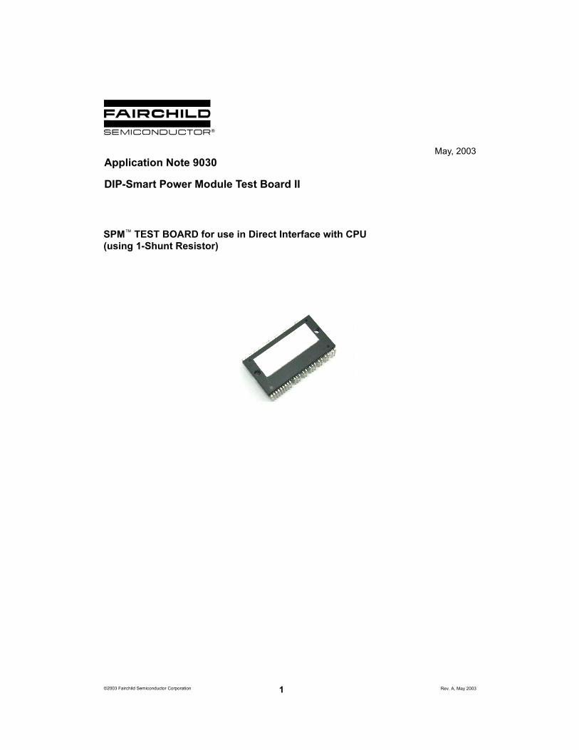
Application Note 9030
DIP-Smart Power Module Test Board II
May, 2003
Rev. A, May 20031©2003 Fairchild Semiconductor Corporation
SPM™ TEST BOARD for use in Direct Interface with CPU(using 1-Shunt Resistor)
2
Rev. A, May 2003©2003 Fairchild Semiconductor Corporation
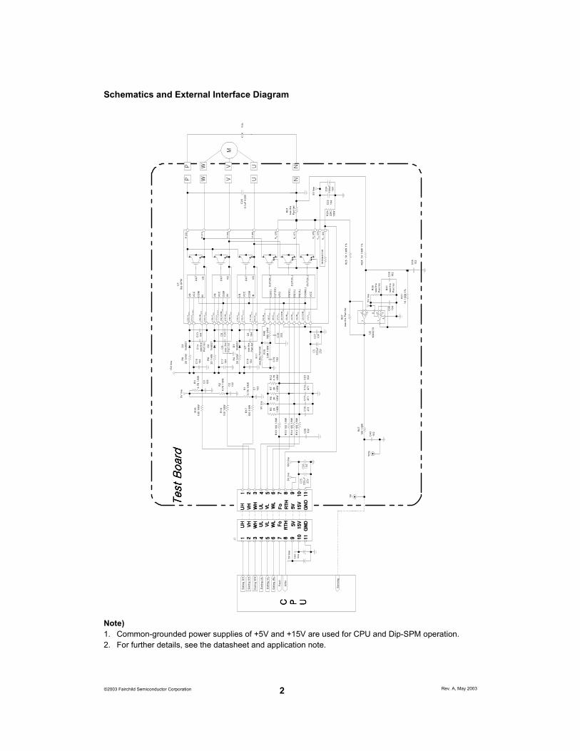
Schematics and External Interface Diagram
Note) 1. Common-grounded power supplies of +5V and +15V are used for CPU and Dip-SPM operation.2. For further details, see the datasheet and application note.
R13
100
1/8
W
R14
100
1/8
W
15V
line
C14
see
the
Par
t lis
t
C13
104
R9
20 1
/4W
D3
1N49
37
C9
see the
Part lis
t
C8
104
R8
20 1
/4W
D2
1N49
37
C7
see
the
Par
t lis
tC
610
4
R4
20 1
/4W
D1
1N49
37
C5
220uF
35V
C27
104
C15
333
C26
102
R16
100
1/8
W
R15
100
1/8
W
M
Vdc
C20
0.1u
F 63
0V
5V li
ne
R20
22K
1/8W
C24
100u
F16
V
C22
104
Gat
ing
UH
Gat
ing
VH
Gat
ing
WH
C CCC P PPP U UUU
R21
see
the
Par
t lis
t
R10
3.9K
1/8
W
C19
102R
11se
e th
e P
art l
ist
5V li
ne
R12
4.7K
1/8W
C12
471
R7
2K 1/8W
R6
2K 1/8W
R5
2K 1/8W
C11
471
C10
471
C23
102
CO
M(L
)
VC
C
IN(U
L)
IN(V
L)
IN(W
L)
VF
O
C(F
OD
)
C(S
C)
OU
T(U
L)
OU
T(V
L)
OU
T(W
L)
NU (2
6)
NV (2
7)
NW
(28)
U (
29)
V (
30)
W (3
1)
P (
32)
(23)
VS
(W)
(22)
VB
(W)
(19)
VS
(V)
(18)
VB
(V)
(9) C
SC
(8) C
FO
D
(7) V
FO
(5) I
N(W
L)
(4) I
N(V
L)
(3) I
N(U
L)
(2) C
OM
(L)
(1) V
CC
(L)
(10)
RS
C
VT
H (2
5)
RT
H (2
4)
(6) C
OM
(L)
VC
C
VB
OU
TC
OM
VS
IN VB
VS
OU
T
INCO
M
VC
C
VC
C
VB
OU
TC
OM
VS
IN
(21)
VC
C(W
H)
(20)
IN(W
H)
(17)
VC
C(V
H)
(15)
IN(V
H)
(16)
CO
M(H
)
(14)
VS
(U)
(13)
VB
(U)
(12)
VC
C(U
H)
(11)
IN(U
H)
THE
RM
ISTO
R
5V li
ne
C3
122
R3
4.7K
1/8
W
C2
122
R2
4.7K
1/8
W
C1
122
R1
4.7K
1/8
W
R19
100
1/8W
R18
100
1/8W
R17
100
1/8W
C25
220uF
35V
C28
104
5V li
ne15
V li
ne
J1
UH
UH
UH
UH
VH
VH
VH
VH
WH
WH
WH
WH
UL
UL
UL
UL
VL
VL
VL
VL
WL
WL
WL
WL
Fo
Fo
Fo
Fo
RTH
RTH
RTH
RTH
15V
15V
15V
15V
1 111 2 222 3 333 4 444 5 555 6 666 8 888 9 999 10
10
10
107 777
UH
UH
UH
UH
VH
VH
VH
VH
WH
WH
WH
WH
UL
UL
UL
UL
VL
VL
VL
VL WL
WL
WL
WL
Fo
Fo
Fo
Fo
RTH
RTH
RTH
RTH
15V
15V
15V
15V
1 111 2 222 3 333 4 444 5 555 6 666 8 888 9 999 10
10
10
107 777
5V
5V
5V
5V
5V
5V
5V
5V
GN
DG
ND
GN
DG
ND
11
11
11
11
GN
DG
ND
GN
DG
ND
11
11
11
11
P N
P N
WW
VV
UU
Gat
ing
WL
Gat
ing
VL
Gat
ing
UL
Fau
lt
RT
H
Sen
sing
15V
line
5V li
ne
Test
Board
Test
Board
Test
Board
Test
Board
C16
104
C17
104
C18
104
R25
1K
1/8
W 1
%
R24
1K
1/8
W 1
%
R31
1K 1
/8W
1%
C36
102
7
56- +
1
438 2
- +
R37
see
the
Par
t lis
t
R47
100
1/8W
C43
102
U2
KM
4270
5V li
ne
C40
104
R41
see
the
Par
t lis
t
R36
see
the
Par
t lis
t
C39
102
TP
TP
G
U1
Dip
-SP
M
R48
390
1/8W
Rev. A, May 20033©2003 Fairchild Semiconductor Corporation
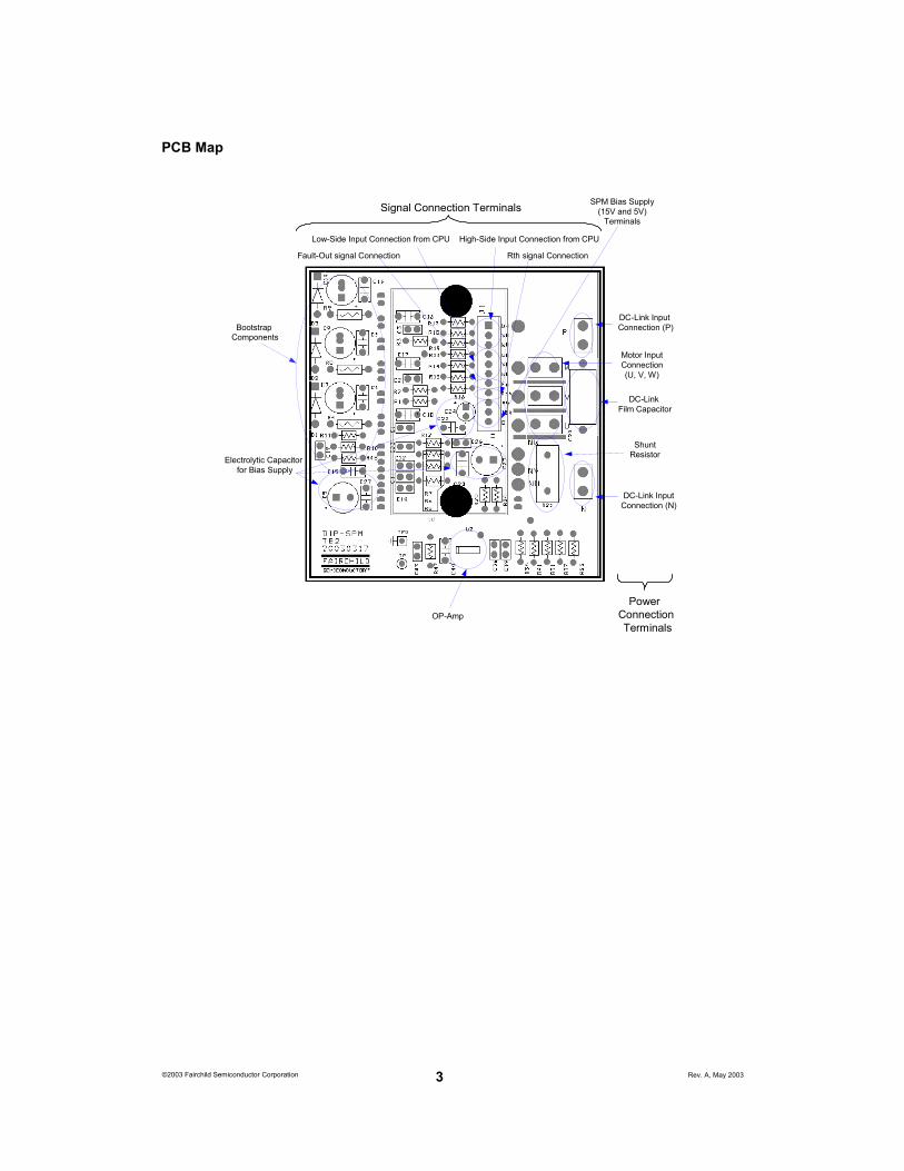
PCB Map
Low-Side Input Connection from CPU
Fault-Out signal Connection
High-Side Input Connection from CPU
Power ConnectionTerminals
Motor Input Connection(U, V, W)
SPM Bias Supply(15V and 5V)
Terminals
Electrolytic Capacitor for Bias Supply
Signal Connection Terminals
DC-Link Input Connection (P)
DC-Link Film Capacitor
Bootstrap Components
Rth signal Connection
DC-Link Input Connection (N)
ShuntResistor
OP-Amp
4
Rev. A, May 2003©2003 Fairchild Semiconductor Corporation
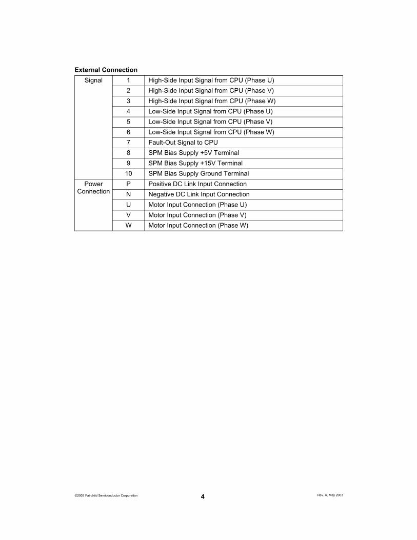
External ConnectionSignal 1 High-Side Input Signal from CPU (Phase U)
2 High-Side Input Signal from CPU (Phase V)3 High-Side Input Signal from CPU (Phase W)4 Low-Side Input Signal from CPU (Phase U)5 Low-Side Input Signal from CPU (Phase V)6 Low-Side Input Signal from CPU (Phase W)7 Fault-Out Signal to CPU8 SPM Bias Supply +5V Terminal9 SPM Bias Supply +15V Terminal
10 SPM Bias Supply Ground TerminalPower
ConnectionP Positive DC Link Input ConnectionN Negative DC Link Input ConnectionU Motor Input Connection (Phase U)V Motor Input Connection (Phase V)W Motor Input Connection (Phase W)
Rev. A, May 20035©2003 Fairchild Semiconductor Corporation
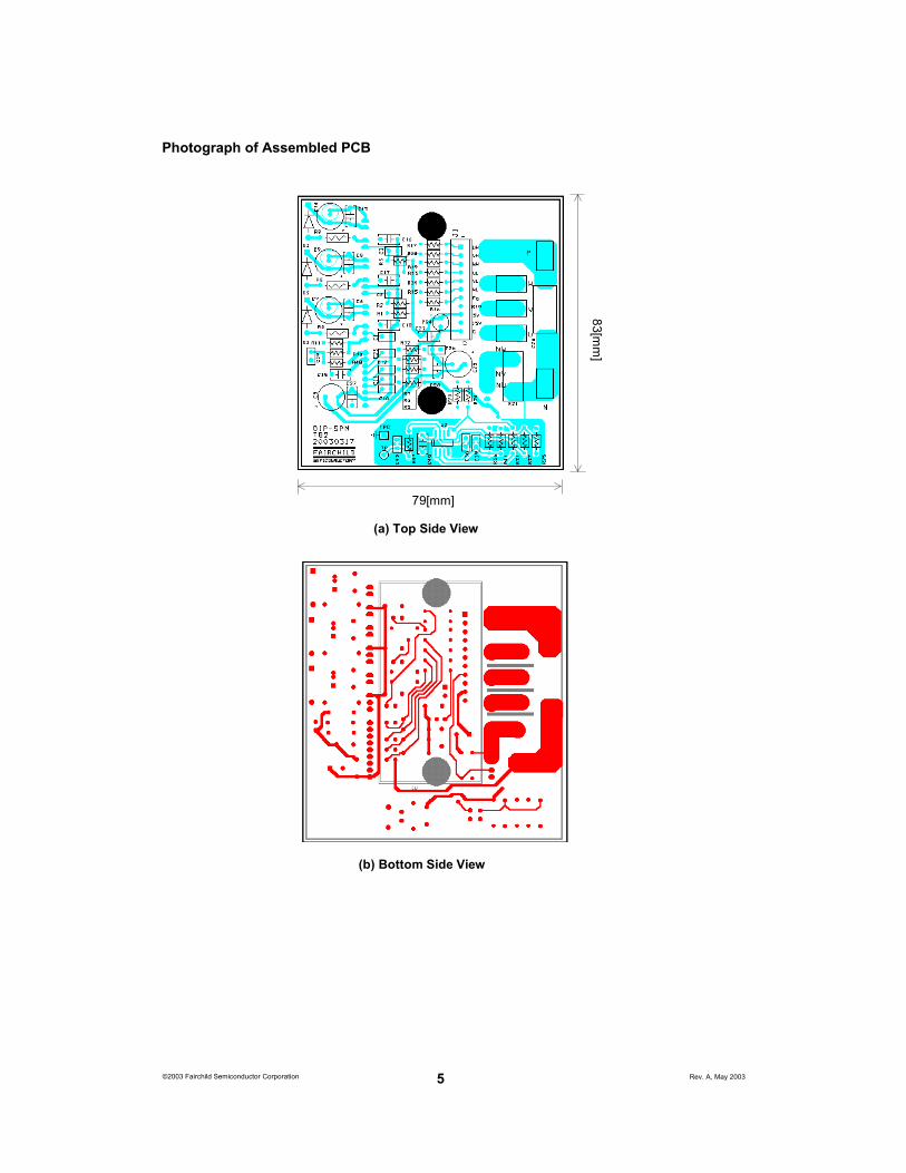
Photograph of Assembled PCB
83[mm
]
79[mm]
(a) Top Side View
(b) Bottom Side View
6
Rev. A, May 2003©2003 Fairchild Semiconductor Corporation
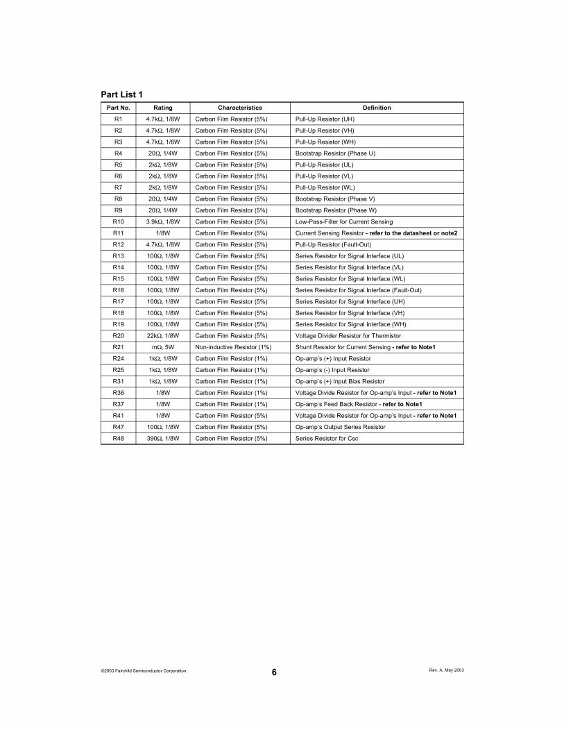
Part List 1Part No. Rating Characteristics Definition
R1 4.7kΩ, 1/8W Carbon Film Resistor (5%) Pull-Up Resistor (UH)
R2 4.7kΩ, 1/8W Carbon Film Resistor (5%) Pull-Up Resistor (VH)
R3 4.7kΩ, 1/8W Carbon Film Resistor (5%) Pull-Up Resistor (WH)
R4 20Ω, 1/4W Carbon Film Resistor (5%) Bootstrap Resistor (Phase U)
R5 2kΩ, 1/8W Carbon Film Resistor (5%) Pull-Up Resistor (UL)
R6 2kΩ, 1/8W Carbon Film Resistor (5%) Pull-Up Resistor (VL)
R7 2kΩ, 1/8W Carbon Film Resistor (5%) Pull-Up Resistor (WL)
R8 20Ω, 1/4W Carbon Film Resistor (5%) Bootstrap Resistor (Phase V)
R9 20Ω, 1/4W Carbon Film Resistor (5%) Bootstrap Resistor (Phase W)
R10 3.9kΩ, 1/8W Carbon Film Resistor (5%) Low-Pass-Filter for Current Sensing
R11 1/8W Carbon Film Resistor (5%) Current Sensing Resistor - refer to the datasheet or note2
R12 4.7kΩ, 1/8W Carbon Film Resistor (5%) Pull-Up Resistor (Fault-Out)
R13 100Ω, 1/8W Carbon Film Resistor (5%) Series Resistor for Signal Interface (UL)
R14 100Ω, 1/8W Carbon Film Resistor (5%) Series Resistor for Signal Interface (VL)
R15 100Ω, 1/8W Carbon Film Resistor (5%) Series Resistor for Signal Interface (WL)
R16 100Ω, 1/8W Carbon Film Resistor (5%) Series Resistor for Signal Interface (Fault-Out)
R17 100Ω, 1/8W Carbon Film Resistor (5%) Series Resistor for Signal Interface (UH)
R18 100Ω, 1/8W Carbon Film Resistor (5%) Series Resistor for Signal Interface (VH)
R19 100Ω, 1/8W Carbon Film Resistor (5%) Series Resistor for Signal Interface (WH)
R20 22kΩ, 1/8W Carbon Film Resistor (5%) Voltage Divider Resistor for Thermistor
R21 mΩ, 5W Non-inductive Resistor (1%) Shunt Resistor for Current Sensing - refer to Note1
R24 1kΩ, 1/8W Carbon Film Resistor (1%) Op-amp’s (+) Input Resistor
R25 1kΩ, 1/8W Carbon Film Resistor (1%) Op-amp’s (-) Input Resistor
R31 1kΩ, 1/8W Carbon Film Resistor (1%) Op-amp’s (+) Input Bias Resistor
R36 1/8W Carbon Film Resistor (1%) Voltage Divide Resistor for Op-amp’s Input - refer to Note1
R37 1/8W Carbon Film Resistor (1%) Op-amp’s Feed Back Resistor - refer to Note1
R41 1/8W Carbon Film Resistor (5%) Voltage Divide Resistor for Op-amp’s Input - refer to Note1
R47 100Ω, 1/8W Carbon Film Resistor (5%) Op-amp’s Output Series Resistor
R48 390Ω, 1/8W Carbon Film Resistor (5%) Series Resistor for Csc
Rev. A, May 20037©2003 Fairchild Semiconductor Corporation
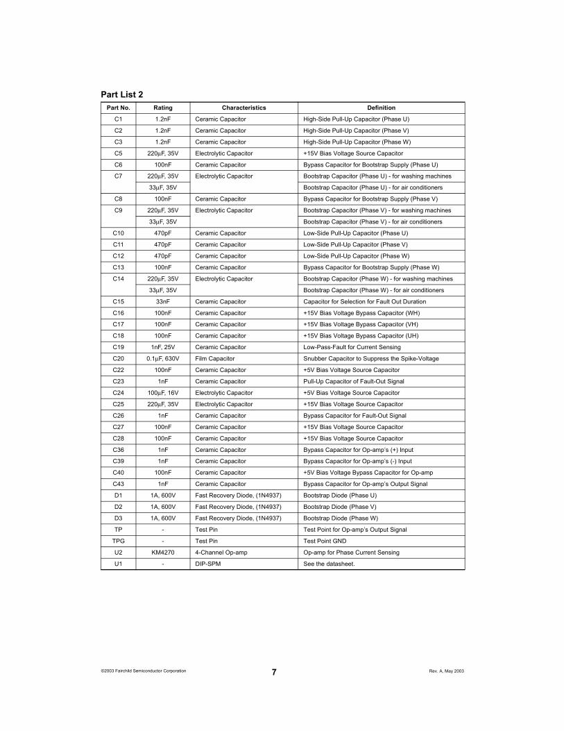
Part List 2Part No. Rating Characteristics Definition
C1 1.2nF Ceramic Capacitor High-Side Pull-Up Capacitor (Phase U)
C2 1.2nF Ceramic Capacitor High-Side Pull-Up Capacitor (Phase V)
C3 1.2nF Ceramic Capacitor High-Side Pull-Up Capacitor (Phase W)
C5 220µF, 35V Electrolytic Capacitor +15V Bias Voltage Source Capacitor
C6 100nF Ceramic Capacitor Bypass Capacitor for Bootstrap Supply (Phase U)
C7 220µF, 35V Electrolytic Capacitor Bootstrap Capacitor (Phase U) - for washing machines
33µF, 35V Bootstrap Capacitor (Phase U) - for air conditioners
C8 100nF Ceramic Capacitor Bypass Capacitor for Bootstrap Supply (Phase V)
C9 220µF, 35V Electrolytic Capacitor Bootstrap Capacitor (Phase V) - for washing machines
33µF, 35V Bootstrap Capacitor (Phase V) - for air conditioners
C10 470pF Ceramic Capacitor Low-Side Pull-Up Capacitor (Phase U)
C11 470pF Ceramic Capacitor Low-Side Pull-Up Capacitor (Phase V)
C12 470pF Ceramic Capacitor Low-Side Pull-Up Capacitor (Phase W)
C13 100nF Ceramic Capacitor Bypass Capacitor for Bootstrap Supply (Phase W)
C14 220µF, 35V Electrolytic Capacitor Bootstrap Capacitor (Phase W) - for washing machines
33µF, 35V Bootstrap Capacitor (Phase W) - for air conditioners
C15 33nF Ceramic Capacitor Capacitor for Selection for Fault Out Duration
C16 100nF Ceramic Capacitor +15V Bias Voltage Bypass Capacitor (WH)
C17 100nF Ceramic Capacitor +15V Bias Voltage Bypass Capacitor (VH)
C18 100nF Ceramic Capacitor +15V Bias Voltage Bypass Capacitor (UH)
C19 1nF, 25V Ceramic Capacitor Low-Pass-Fault for Current Sensing
C20 0.1µF, 630V Film Capacitor Snubber Capacitor to Suppress the Spike-Voltage
C22 100nF Ceramic Capacitor +5V Bias Voltage Source Capacitor
C23 1nF Ceramic Capacitor Pull-Up Capacitor of Fault-Out Signal
C24 100µF, 16V Electrolytic Capacitor +5V Bias Voltage Source Capacitor
C25 220µF, 35V Electrolytic Capacitor +15V Bias Voltage Source Capacitor
C26 1nF Ceramic Capacitor Bypass Capacitor for Fault-Out Signal
C27 100nF Ceramic Capacitor +15V Bias Voltage Source Capacitor
C28 100nF Ceramic Capacitor +15V Bias Voltage Source Capacitor
C36 1nF Ceramic Capacitor Bypass Capacitor for Op-amp’s (+) Input
C39 1nF Ceramic Capacitor Bypass Capacitor for Op-amp’s (-) Input
C40 100nF Ceramic Capacitor +5V Bias Voltage Bypass Capacitor for Op-amp
C43 1nF Ceramic Capacitor Bypass Capacitor for Op-amp’s Output Signal
D1 1A, 600V Fast Recovery Diode, (1N4937) Bootstrap Diode (Phase U)
D2 1A, 600V Fast Recovery Diode, (1N4937) Bootstrap Diode (Phase V)
D3 1A, 600V Fast Recovery Diode, (1N4937) Bootstrap Diode (Phase W)
TP - Test Pin Test Point for Op-amp’s Output Signal
TPG - Test Pin Test Point GND
U2 KM4270 4-Channel Op-amp Op-amp for Phase Current Sensing
U1 - DIP-SPM See the datasheet.
8
Rev. A, May 2003©2003 Fairchild Semiconductor Corporation
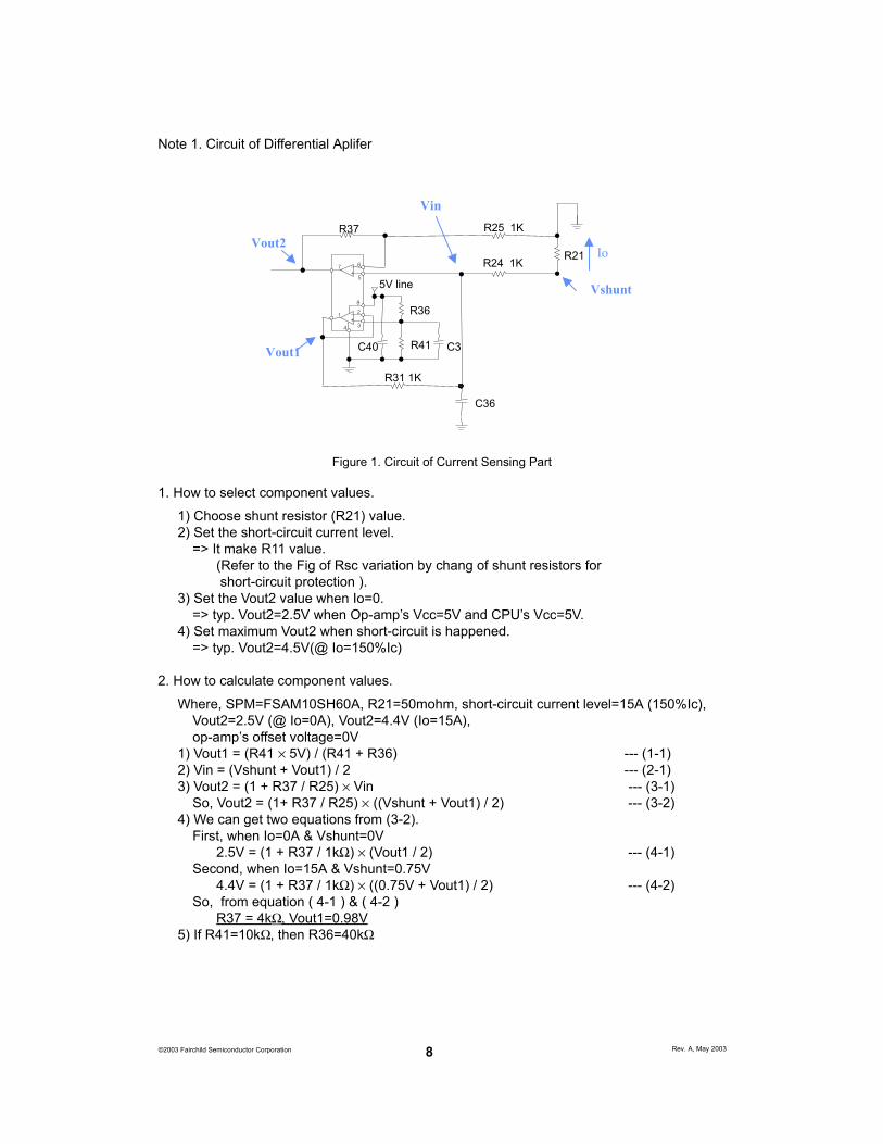
Note 1. Circuit of Differential Aplifer
Figure 1. Circuit of Current Sensing Part
1. How to select component values.1) Choose shunt resistor (R21) value.2) Set the short-circuit current level.
=> It make R11 value.(Refer to the Fig of Rsc variation by chang of shunt resistors for short-circuit protection ).
3) Set the Vout2 value when Io=0.=> typ. Vout2=2.5V when Op-amp’s Vcc=5V and CPU’s Vcc=5V.
4) Set maximum Vout2 when short-circuit is happened.=> typ. Vout2=4.5V(@ Io=150%Ic)
2. How to calculate component values.
Where, SPM=FSAM10SH60A, R21=50mohm, short-circuit current level=15A (150%Ic),Vout2=2.5V (@ Io=0A), Vout2=4.4V (Io=15A),op-amp’s offset voltage=0V
1) Vout1 = (R41 × 5V) / (R41 + R36) --- (1-1)2) Vin = (Vshunt + Vout1) / 2 --- (2-1)3) Vout2 = (1 + R37 / R25) × Vin --- (3-1)
So, Vout2 = (1+ R37 / R25) × ((Vshunt + Vout1) / 2) --- (3-2)4) We can get two equations from (3-2).
First, when Io=0A & Vshunt=0V2.5V = (1 + R37 / 1kΩ) × (Vout1 / 2) --- (4-1)
Second, when Io=15A & Vshunt=0.75V 4.4V = (1 + R37 / 1kΩ) × ((0.75V + Vout1) / 2) --- (4-2)
So, from equation ( 4-1 ) & ( 4-2 )R37 = 4kΩ, Vout1=0.98V
5) If R41=10kΩ, then R36=40kΩ
R21
R25 1K
R24 1K
R31 1K
C36
7
5
6-+
1
4 3
8
2-+
R37
5V line
C40 R41
R36
C3
Vshunt
Vout1
Vout2
Vin
Io
Rev. A, May 20039©2003 Fairchild Semiconductor Corporation
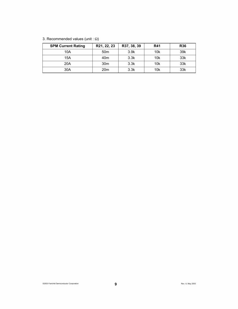
3. Recommended values (unit : Ω)
SPM Current Rating R21, 22, 23 R37, 38, 39 R41 R3610A 50m 3.9k 10k 39k15A 40m 3.3k 10k 33k20A 30m 3.3k 10k 33k30A 20m 3.3k 10k 33k
10
Rev. A, May 2003©2003 Fairchild Semiconductor Corporation
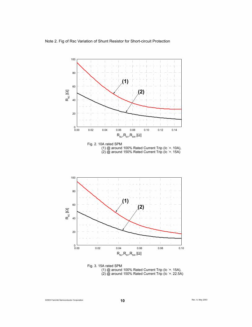
Note 2. Fig of Rsc Variation of Shunt Resistor for Short-circuit Protection
Fig. 2. 10A rated SPM(1) @ around 100% Rated Current Trip (Ic ·=· 10A),(2) @ around 150% Rated Current Trip (Ic ·=· 15A)
Fig. 3. 15A rated SPM(1) @ around 100% Rated Current Trip (Ic ·=· 15A),(2) @ around 150% Rated Current Trip (Ic ·=· 22.5A)
0.00 0.02 0.04 0.06 0.08 0.10 0.12 0.140
20
40
60
80
100
(2)
(1)
R SC [ Ω
]
RSU,RSV,RSW [Ω]
0.00 0.02 0.04 0.06 0.08 0.100
20
40
60
80
100
(2)(1)
R SC [Ω
]
RSU,RSV,RSW [Ω]
Rev. A, May 200311©2003 Fairchild Semiconductor Corporation
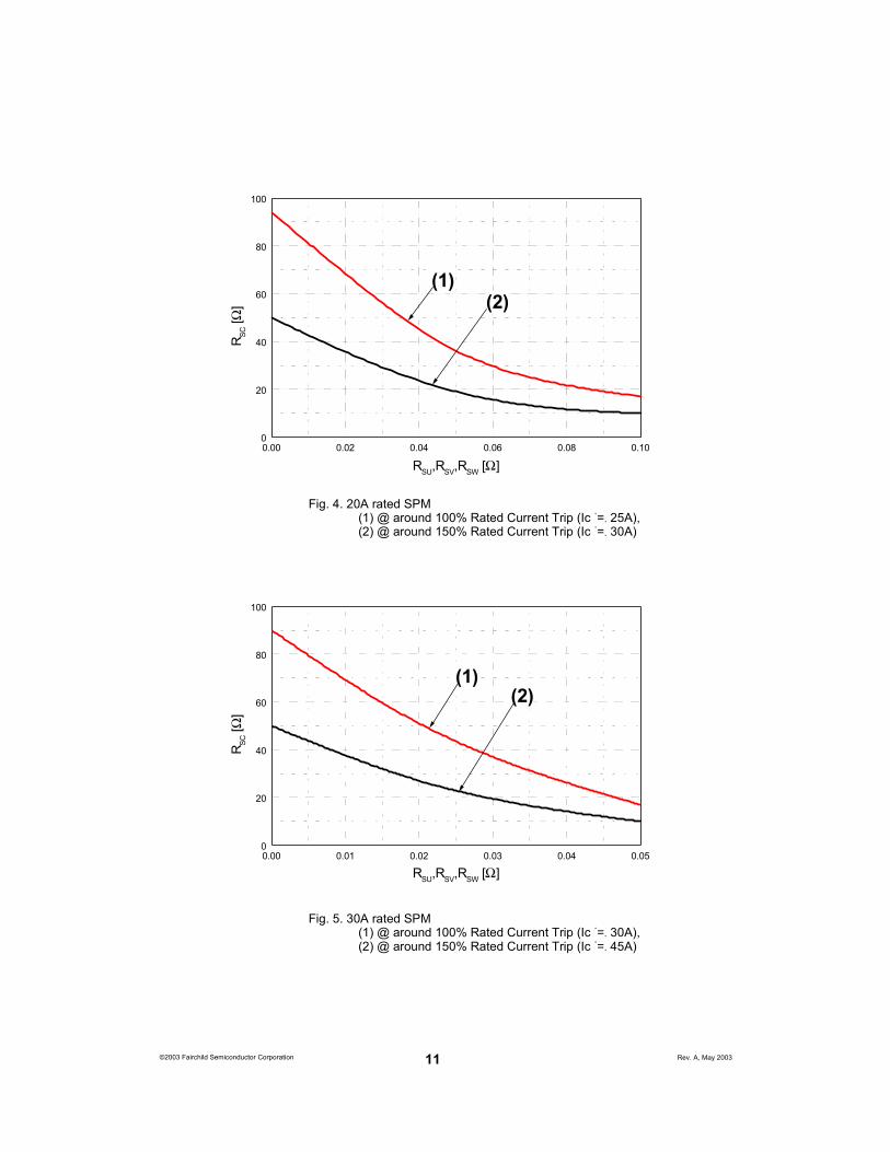
Fig. 4. 20A rated SPM(1) @ around 100% Rated Current Trip (Ic ·=· 25A),(2) @ around 150% Rated Current Trip (Ic ·=· 30A)
Fig. 5. 30A rated SPM(1) @ around 100% Rated Current Trip (Ic ·=· 30A),(2) @ around 150% Rated Current Trip (Ic ·=· 45A)
0.00 0.02 0.04 0.06 0.08 0.100
20
40
60
80
100
(2)(1)
R SC [Ω
]
RSU,RSV,RSW [Ω]
0.00 0.01 0.02 0.03 0.04 0.050
20
40
60
80
100
(2)(1)
R SC [Ω
]
RSU,RSV,RSW [Ω]
!"#$%"&'(%& %)'"%&'!%*$%('((!'&$$%"'+'%,'*- %& ''.$'-'($$%+!% !"'*%("&%%$%%( /0!11 2 2345 123 4511 3 45 1 1 1 2 1 3 21 6 2
7 12111 2 1 21 11 23 2
$ 2
((
%
1 1 1122
1 2311 21 2 1
1 2 1
11 2 1 2
"
$
$
($
!"# !
$ %
& '() *
+
,-./,0
"""! "# !1+# !%
!
0#23#24#25((+
# 6%6
7! 0!$8!#! 0!,80!,!0+$! '!