Embed Size (px)
Citation preview

To learn more about ON Semiconductor, please visit our website at www.onsemi.com
Is Now Part of
ON Semiconductor and the ON Semiconductor logo are trademarks of Semiconductor Components Industries, LLC dba ON Semiconductor or its subsidiaries in the United States and/or other countries. ON Semiconductor owns the rights to a number of patents, trademarks, copyrights, trade secrets, and other intellectual property. A listing of ON Semiconductor’s product/patent coverage may be accessed at www.onsemi.com/site/pdf/Patent-Marking.pdf. ON Semiconductor reserves the right to make changes without further notice to any products herein. ON Semiconductor makes no warranty, representation or guarantee regarding the suitability of its products for any particular purpose, nor does ON Semiconductor assume any liability arising out of the application or use of any product or circuit, and specifically disclaims any and all liability, including without limitation special, consequential or incidental damages. Buyer is responsible for its products and applications using ON Semiconductor products, including compliance with all laws, regulations and safety requirements or standards, regardless of any support or applications information provided by ON Semiconductor. “Typical” parameters which may be provided in ON Semiconductor data sheets and/or specifications can and do vary in different applications and actual performance may vary over time. All operating parameters, including “Typicals” must be validated for each customer application by customer’s technical experts. ON Semiconductor does not convey any license under its patent rights nor the rights of others. ON Semiconductor products are not designed, intended, or authorized for use as a critical component in life support systems or any FDA Class 3 medical devices or medical devices with a same or similar classification in a foreign jurisdiction or any devices intended for implantation in the human body. Should Buyer purchase or use ON Semiconductor products for any such unintended or unauthorized application, Buyer shall indemnify and hold ON Semiconductor and its officers, employees, subsidiaries, affiliates, and distributors harmless against all claims, costs, damages, and expenses, and reasonable attorney fees arising out of, directly or indirectly, any claim of personal injury or death associated with such unintended or unauthorized use, even if such claim alleges that ON Semiconductor was negligent regarding the design or manufacture of the part. ON Semiconductor is an Equal Opportunity/Affirmative Action Employer. This literature is subject to all applicable copyright laws and is not for resale in any manner.

www.fairchildsemi.com
© 2009 Fairchild Semiconductor Corporation www.fairchildsemi.com Rev. 1.0.1 • 6/1/10
AN-8021 Building Variable Output Voltage Boost PFC Converters with the FAN9612 Interleaved BCM PFC Controller Abstract The output voltage of a boost PFC converter has to be set above the highest input voltage of the source in order to maintain boost operation and be able to shape the input current waveform of the power supply. For universal input voltage designs, the appropriate output voltage selection is about 400VDC. In many applications, it might be desirable to adjust the output voltage according to the input AC rms voltage level, the output power of the converter, or both. The FAN9612 Interleaved BCM PFC controller is particularly suited to implement such designs because the non-inverting input of the voltage error amplifier is easily accessible to adjust the converter’s output voltage. This application note gives details about how to make the boost output voltage the function of the output power of the converter. Circuits with variable level of sophistications are shown and explained. Furthermore, it describes the design and implementation of the boost follower concept where the output voltage becomes the function of the input AC rms voltage level.
Why Adjust VOUT? The output voltage of the Power Factor Correctors (PFC) front-end is defined by many requirements and operating parameters of the power supply. PFCs draw power from the input source following a sine square function while their output is loaded with a practically constant load, as depicted in Figure 1.
Figure 1. Instantaneous Input and Output Power
of a PFC Front-End
Therefore, energy storage must take place in the power factor corrector on the line frequency basis. This energy storage is most efficient at high output voltage, such as 400VDC. On the other hand, the switching losses of the boost converter and the downstream isolated DC-DC converter are both proportional to the output voltage of the PFC. Higher output voltage increases switching losses, which is most noticeable in the light-load efficiency of the
power supplies. Consequently, the output voltage should be kept the minimum allowed by the fundamental requirements to maintain feasible operating conditions for the boost converter.
These opposing requirements of:
keeping the output voltage above the highest input voltage level;
using the highest possible voltage to improve volumetric efficiency of energy storage; and
lowering switching losses by selecting the lowest possible output voltage;
might lead to the implementation of a system where the boost output voltage is optimized for the momentary input voltage and load conditions. These solutions are the focus of this application note.
How to Adjust VOUT? The FAN9612 is unique among the PFC controllers because of the full accessibility of its error amplifier. In addition to the inverting input (FB) and the output of the error amplifier (COMP), which must be available for output voltage sensing and compensation, the non-inverting input (SS) is also accessible, as shown in Figure 2.
The non-inverting input of the error amplifier is connected to a voltage reference (VSS) generated across the soft-start capacitor (CSS). The feedback divider (RFB1 and RFB2) is connected to the inverting input of the error amplifier through the FB pin. The reference voltage, together with the feedback resistors, sets the desired output voltage according to the expression depicted in Figure 2.
AN-8021 APPLICATION NOTE
© 2009 Fairchild Semiconductor Corporation www.fairchildsemi.com Rev. 1.0.1 • 6/1/10 2
Figure 2. External Connections of the Error Amplifier
The FAN9612 allows the output voltage of the converter to be adjusted either by modifying the feedback network or by changing the reference voltage.
Changing the feedback divider gain affects the closed-loop gain of the converter; thus, it can cause stability problems or set unacceptable limitations on the control loop bandwidth. Conversely, changing the reference of the error amplifier has no effect on the loop gain and utilizes the same mechanism used during the closed-loop soft-start of the converter. Furthermore, this approach does not affect the over-voltage protection levels of the converter.
While either method can vary the output voltage of the converter, changing the reference of the error amplifier is a better solution.
When to Lower VOUT and How Low to Adjust? The output voltage of the power factor corrector is carefully selected to meet the design requirements. Nevertheless, there are certain combinations of operating conditions that would allow adjusting the converter’s output voltage lower to benefit from reduced switching losses. For instance, when the input voltage is not at its maximum value, the boost output voltage could be reduced; but the effects of the lower output voltage on the system must be carefully considered. One of the factors that must be taken into account is the required hold-up time, a specification which defines that the output voltage must stay above a minimum level for a predetermined length of time in case the input voltage suddenly disappears. This minimum voltage is a function of the operating input voltage range of the downstream isolated DC-DC power supply. This system-level specification primarily influences the value of the energy storage capacitor at the output of the PFC, which also serves as the input capacitance for the downstream converter. Usually, the capacitance is calculated for the worst-case condition when the system delivers full output power. It can be estimated as:
2MINOUT,
2NOMOUT,
UPHOLDMAXOUT,OUT VV
tP2C
−
⋅⋅= (1)
When the output voltage is kept constant, the resulting hold-up time is longer than required at lighter load conditions. For a given power stage design where the capacitor value is fixed, it is possible to lower the output voltage of the power factor corrector under light-load conditions without violating the hold-up time specification:
( )2MINOUT,
2NOMOUT,NORMOUT,
2MINOUT,
NORMOUT,OUT
VVPV
)(PV
−⋅+
= (2)
where
MAXOUT,
OUTNORMOUT, P
PP = (3)
is the normalized output power of the PFC converter. Assuming 400VDC for the nominal output voltage and 340VDC as the minimum at the end of the hold-up time, Figure 3 shows the solution for the minimum boost output voltage as a function of the normalized output power to maintain the hold-up time requirement for the system.
POUT (normalized)
VOUT
340V
360V
380V
400V
0 1
Figure 3. Boost Output Voltage as a Function of Normalized Load Conditions (tHOLD UP=constant)
It is important to notice that, despite the square root function in the exact mathematical solution, the graph shows a nearly linear relationship between the normalized output power and the output voltage of the converter. In fact, the output voltage can be accurately estimated by:
( )MINOUT,NOMOUT,NORMOUT,MINOUT,
NORMOUT,LINOUT,
VVPV
)(PV
−⋅+
= (4)
The error between the linearly approximated output voltage in Equation (4) and the exact solution given in Equation (2) remains well below 1% under all load conditions, as illustrated in Figure 4.

AN-8021 APPLICATION NOTE
© 2009 Fairchild Semiconductor Corporation www.fairchildsemi.com Rev. 1.0.1 • 6/1/10 3
POUT (normalized)0 10
0.1
0.2
0.3
0.4
Error[%]
Figure 4. Percentage Error Between the Output
Voltages Given by Equations (2) and (4)
The important conclusion of the presented analysis is that the output voltage can be a linear function of the output power. This finding eases the circuit implementation to vary the output voltage according to the load conditions. The FAN9612 controller makes this task even easier since its control technique utilizes input voltage feed-forward. The output of its error amplifier is directly proportional to the output power of the supply.
Another consequence of lowering the boost power factor corrector’s output voltage as a function of the output power might become apparent during rapid load increase. Due to the doubled line frequency ripple across the output capacitor, PFC converters employ an extremely slow voltage regulation loop. Typical voltage loop bandwidth is around 10Hz in PFC applications. In contrast, the control loop bandwidth of the downstream DC-DC converter is approximately two orders of magnitude higher, typically a few kHz. As a result, it is unavoidable that the boost output voltage sags temporarily in response to quickly increasing output power demand. If the output voltage of the PFC converter was low due to the preceding light-load operation, the output voltage transient window is severely limited before the input under-voltage protection threshold of the downstream converter is activated. Therefore, the adjustment range of the boost output voltage has to be carefully selected and the light-load operating voltage must be kept sufficiently above the minimum input voltage (VOUT,MIN) of the DC-DC converter to accommodate output voltage variations during load transients.
VOUT
100V
200V
300V
400V
VIN,PK
VIN,RMS265V65V
Figure 5. Output Voltage Set Point of the Boost
Follower
In some instances, when the downstream DC-DC converter works acceptably over a wide input voltage range, it could be possible to adjust the boost output voltage as a function of the input AC rms voltage. This implementation is called the boost follower, where the PFC output voltage is proportional to the rms value of the AC input voltage. Figure 5 shows a potential approach where the boost output voltage is set above the peak input voltage level by a fixed offset.
The example highlights the wide PFC output voltage variation of this technique, which can present a challenge designing the downstream converter. Furthermore, an almost 3:1 output voltage variation between 400VDC and approximately 140VDC, as shown in Figure 5, results in energy storage variation of 9:1 at the output of the PFC converter. At the low end of the output voltage range, the doubled line frequency ripple would increase significantly further, escalating the required input voltage range of the DC-DC converter connected to the PFC output. Hold-up time capability would also be significantly impaired at low line, unless the output capacitance is significantly increased. Note that the higher output capacitance value would have a positive effect on the ripple amplitude as well. Furthermore, the previously outlined hold-up time and transient considerations are equally applicable in the boost follower applications.
Table 1. Comparison of Output Voltage Adjustment Strategies
Boost Follower Load Dependent Output VOUT Function VOUT (VIN,RMS) VOUT (POUT) VOUT Range Wide Narrow Output Capacitance Large, based on output ripple Small, based on hold-up time Hold-up Time Strong function of VIN,RMS Per specification Transient Response Strong function of VIN,RMS Weak function of POUT DC-DC Input Range Wide Narrow
AN-8021 APPLICATION NOTE
© 2009 Fairchild Semiconductor Corporation www.fairchildsemi.com Rev. 1.0.1 • 6/1/10 4
The difference between the boost follower implementation and adjusting the output voltage according to the load is summarized in Table 1.
Although it was not directly emphasized, the instantaneous peak input voltage of the PFC stage and the minimum operating input voltage of the downstream converter always limit the boost output voltage adjustment range.
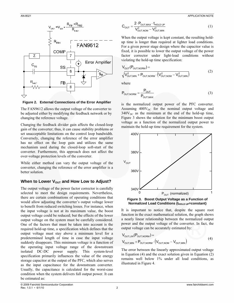
Simple VOUT Adjust by POUT As mentioned earlier, the error amplifier output of the FAN9612 BCM PFC controller is proportional to the output power of the power stage it controls. The PWM ramp offset in the FAN9612 is approximately 0.2V (VRAMP,OFFSET). When the error amplifier output is below this voltage, no PWM output pulse is generated. Therefore, VCOMP=0.2V corresponds to zero output power. The converter delivers its maximum output power at approximately VCOMP=4.5V. Accordingly, the relationship between the error amplifier’s output voltage and the converter’s output power is given as:
( )NORMOUT,COMPOFFSETRAMP,
NORMOUT,COMP
PΔVVPV
⋅+
= (5)
where ΔVCOMP is the control range of the error amplifier (4.3V).
Utilizing the proportionality between POUT and VCOMP, the output voltage can be easily adjusted. Figure 6 shows one of the simplest implementations that can adjust the boost output voltage to a user-defined minimum level under light-load conditions.
Figure 6. Output Voltage Adjustment by Output Power
The circuit consists of the R1, R2 divider, which sets the lowest output voltage corresponding to no-load conditions. In addition, an “ideal diode” (see Additional Implementation Details toward the end of this application note) formed by the operational amplifier U1 and the diode, D1, connected to its output is used to adjust the reference of the error amplifier across the soft-start capacitor, CSS.
The design procedure starts by choosing the desired output voltage at zero load, VOUT,0 and selecting one of the resistor values, R2 for example. R1 can be found by:
⎟⎟⎟⎟⎟
⎠
⎞
⎜⎜⎜⎜⎜
⎝
⎛
−−⋅
−⋅= 1
VVV
3V
V5VR2R1
OFFSETRAMP,NOMOUT,
OUT,0
OFFSETRAMP, (6)
where VOUT,NOM is the nominal output voltage at full load and VRAMP,OFFSET is the PWM ramp offset found in the FAN9612 datasheet.
While the value of R2 can be selected by the designer, it is important to draw attention to the fact that the R1, R2 divider introduces a DC current into the output of the gM-type error amplifier of the FAN9612. This DC current component must be kept very low to avoid introducing a large voltage regulation error. Typical current levels should be in the μA range, which necessitates that the resistance of R2 is chosen in the 300kΩ to 500kΩ range. The worst-case output voltage regulation error occurs at no load and can be estimated as:
FB2
FB2FB1M
OFFSETRAMP,OFFSETOUT, R
RRgR2R1
V5VV +
⋅⋅+
−= (7)
where gM and VRAMP,OFFSET are datasheet parameters; RFB1 and RFB2 forms the feedback divider according to Figure 2; and R1, R2 resistors are part of the schematic introduced in Figure 6. The performance of the solutions is illustrated in Figure 7.
POUT (normalized)0 1
VOUT
300V
350V
400V
450V
1V
2V
3V
4V
5V
VSS
VCOMP
Figure 7. VSS, VCOMP, and VOUT as a Function of
Normalized Output Power
As Figure 7 shows, the output voltage of the converter is gradually reduced when the load drops below 20% of the maximum output power. VCOMP and VSS are also shown for completeness. While this circuit is very simple and requires only a few external components, the designer can only choose the minimum output voltage level. This circuit does not allow selecting the power level where the output voltage starts decreasing.
AN-8021 APPLICATION NOTE
© 2009 Fairchild Semiconductor Corporation www.fairchildsemi.com Rev. 1.0.1 • 6/1/10 5
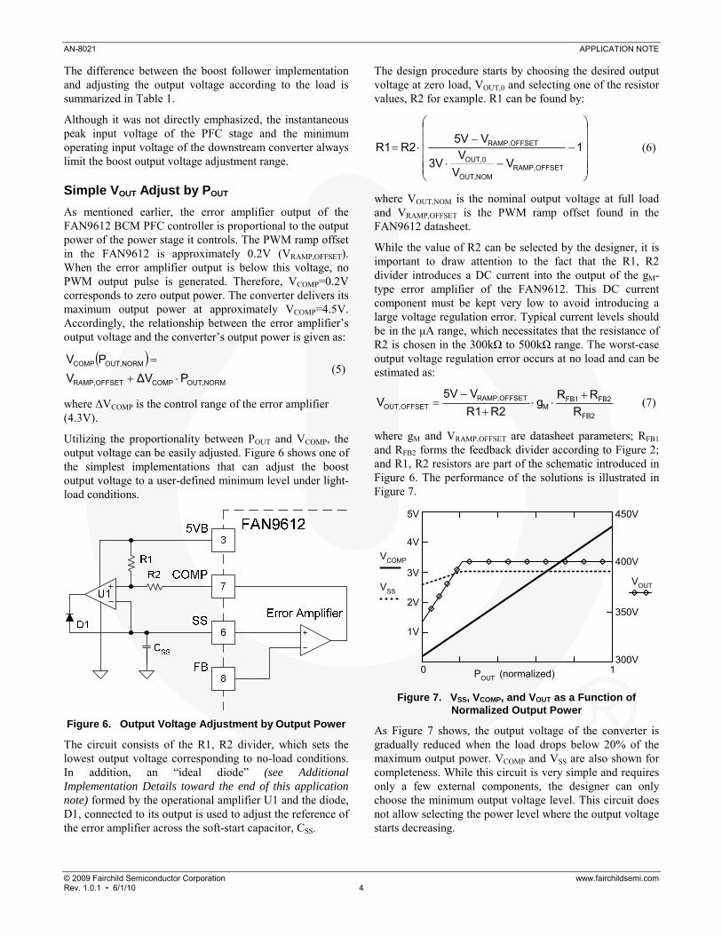
Flexible VOUT Adjust by POUT Adding two additional resistors, R3 and R4, to the circuit shown in Figure 6 offers additional flexibility to consciously pick the output power level where the converter’s output voltage adjustment commences.
3
R1R2
Error Amplifier
FAN9612
8
7
6
COMP
SS
FBCSS
5VBR3
R4
VADJ
U1
D1
Figure 8. Flexible Output Voltage Adjustment by
Output Power
To start the design, two application parameters need to be established and two resistor values to be selected. The output voltage at zero load is VOUT,0, the output power level where the output voltage adjustment begins is PADJ, and they can be part of the power supply specification. In addition, one resistor of each divider can be selected by the designer; for instance, R2 and R4. Notice that the R1, R2 divider current is provided by the R3, R4 divider; therefore, the current flowing through R3 and R4 must be at least two orders of magnitude larger to avoid interaction between the two networks. Fortunately that requirement is aligned perfectly by the restriction to keep the R1, R2 divider current at a low value to avoid output voltage regulation error. The step by step design procedure is outlined in Equations (8) through (12).
The final value of the error amplifier’s reference voltage, VSS,0, corresponding to the output voltage at no load is:
NOMOUT,
OUT,0SS,0 V
V3VV ⋅= (8)
where VOUT,NOM is the nominal output voltage at full load and 3V is the reference voltage of the error amplifier. The error amplifier’s output at the onset of output voltage adjustment can also be determined by:
( )MAXOUT,
ADJCOMPOFFSETRAMP,ADJCOMP P
PΔVVPV ⋅+= (9)
The appropriate value of VADJ, the voltage set by the R3, R4 divider according to the schematic shown in Figure 8, can be calculated as:
( )( ) ( )OFFSETRAMP,ADJCOMPSS,0
OFFSETRAMP,ADJCOMPSS,0ADJ V3VPVV
V3VPVVV
+−+⋅−⋅
= (10)
After selecting R4, typically in the 5 to 10kΩ range, R3 can be defined to set VADJ to the calculated voltage based on:
⎟⎟⎠
⎞⎜⎜⎝
⎛−⋅= 1
V5VR4R3
ADJ
(11)
To ensure that the current of R1 and R2 divider does not influence the voltage established by R3 and R4 (VADJ), select R2=100·R4. The value of R1 is then found by:
⎟⎟⎠
⎞⎜⎜⎝
⎛−
−−
⋅= 1VVVV
R2R1OFFSETRAMP,SS,0
OFFSETRAMP,ADJ (12)
The final circuit performance is demonstrated in Figure 9.
POUT (normalized)0 1
VOUT
300V
350V
400V
450V
1V
2V
3V
4V
5V
VSS
VCOMP
Figure 9. VSS, VCOMP, and VOUT as a Function of
Normalized Output Power
In summary, the circuit shown in Figure 8 accommodates user programmable output voltage adjustment of the boost PFC converter as a function of the output power. The resistive divider comprised by R1 and R2 sets the lowest output voltage level corresponding to no-load condition and the R3, R4 divider determines the power level where the output voltage starts decreasing. The example solution in Figure 9 is designed to reduce VOUT from its nominal 400V to 340V linearly, while the converter’s output power decreases from 70% of its maximum value to zero, respectively.
Universal VOUT Adjust by POUT One potential shortcoming of these solutions is that the programmed output voltage of the boost converter might become lower than the peak of the input voltage. This could occur when high line and low power conditions occur together. At that point, depending on the chosen VOUT,0 level, the boost converter might become a peak rectifier and power factor correction would be lost. To remedy the situation, the input voltage has to be monitored and the information used to limit how low the output voltage can be adjusted.
AN-8021 APPLICATION NOTE
© 2009 Fairchild Semiconductor Corporation www.fairchildsemi.com Rev. 1.0.1 • 6/1/10 6
3
R1R2
Error Amplifier
FAN9612
8
7
6
COMP
SS
FBCSS
5VBR3
R4
VADJ
R6
R7
C1 C2
R5
RIN2
(RIN1-R5)
10VIN
VIN(t)
VLIM
D1
U1
U2
D2
KIN VIN(t)
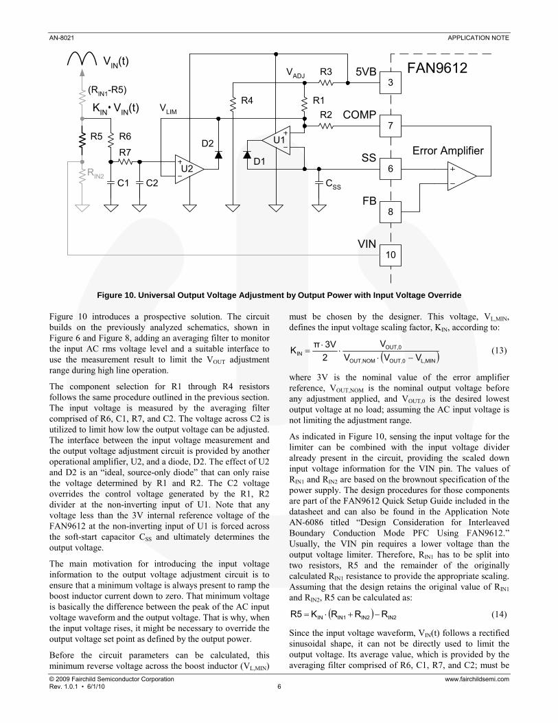
Figure 10. Universal Output Voltage Adjustment by Output Power with Input Voltage Override
Figure 10 introduces a prospective solution. The circuit builds on the previously analyzed schematics, shown in Figure 6 and Figure 8, adding an averaging filter to monitor the input AC rms voltage level and a suitable interface to use the measurement result to limit the VOUT adjustment range during high line operation.
The component selection for R1 through R4 resistors follows the same procedure outlined in the previous section. The input voltage is measured by the averaging filter comprised of R6, C1, R7, and C2. The voltage across C2 is utilized to limit how low the output voltage can be adjusted. The interface between the input voltage measurement and the output voltage adjustment circuit is provided by another operational amplifier, U2, and a diode, D2. The effect of U2 and D2 is an “ideal, source-only diode” that can only raise the voltage determined by R1 and R2. The C2 voltage overrides the control voltage generated by the R1, R2 divider at the non-inverting input of U1. Note that any voltage less than the 3V internal reference voltage of the FAN9612 at the non-inverting input of U1 is forced across the soft-start capacitor CSS and ultimately determines the output voltage.
The main motivation for introducing the input voltage information to the output voltage adjustment circuit is to ensure that a minimum voltage is always present to ramp the boost inductor current down to zero. That minimum voltage is basically the difference between the peak of the AC input voltage waveform and the output voltage. That is why, when the input voltage rises, it might be necessary to override the output voltage set point as defined by the output power.
Before the circuit parameters can be calculated, this minimum reverse voltage across the boost inductor (VL,MIN)
must be chosen by the designer. This voltage, VL,MIN, defines the input voltage scaling factor, KIN, according to:
( )MINL,OUT,0NOMOUT,
OUT,0IN VVV
V23VπK
−⋅⋅
⋅= (13)
where 3V is the nominal value of the error amplifier reference, VOUT,NOM is the nominal output voltage before any adjustment applied, and VOUT,0 is the desired lowest output voltage at no load; assuming the AC input voltage is not limiting the adjustment range.
As indicated in Figure 10, sensing the input voltage for the limiter can be combined with the input voltage divider already present in the circuit, providing the scaled down input voltage information for the VIN pin. The values of RIN1 and RIN2 are based on the brownout specification of the power supply. The design procedures for those components are part of the FAN9612 Quick Setup Guide included in the datasheet and can also be found in the Application Note AN-6086 titled “Design Consideration for Interleaved Boundary Conduction Mode PFC Using FAN9612.” Usually, the VIN pin requires a lower voltage than the output voltage limiter. Therefore, RIN1 has to be split into two resistors, R5 and the remainder of the originally calculated RIN1 resistance to provide the appropriate scaling. Assuming that the design retains the original value of RIN1 and RIN2, R5 can be calculated as:
( ) IN2IN2IN1IN RRRKR5 −+⋅= (14)
Since the input voltage waveform, VIN(t) follows a rectified sinusoidal shape, it can not be directly used to limit the output voltage. Its average value, which is provided by the averaging filter comprised of R6, C1, R7, and C2; must be
AN-8021 APPLICATION NOTE
© 2009 Fairchild Semiconductor Corporation www.fairchildsemi.com Rev. 1.0.1 • 6/1/10 7
used. These components implement a two-stage low-pass filter. The filter design is based on the lowest frequency of the input AC source, fLINE,MIN. The filter’s recommended corner frequency can be set according to:
MINLINE,P f0.15f ⋅= (15)
The component values are defined by:
C1fπ21R7R6
C2C1
P ⋅⋅⋅==
= (16)
where C1 should be selected to ensure that the resistor values (R6 and R7) are in the 500kΩ range. It is necessary that the filter does not load the input voltage divider; thus R6 and R7 must be high impedances. Since the filter network does not utilize any resistor connected to GND, it does not cause any measurement error in the functions based on the accurate scaling of the input voltage for the VIN pin. Assuming that the minimum line frequency is 47Hz, the recommended component values are C1=C2=47nF and R6=R7=470kΩ.
The combined effect of input voltage and output power variations yields the output characteristic shown in Figure 11.
Figure 11. VSS, VOUT, and VIN,PEAK as a Function
of the Input rms Voltage
As Figure 11 illustrates, the output voltage of the converter is adjusted according to the output load as long as the peak of the input AC voltage waveform stays at least 40V below the desired output voltage. At high AC line conditions, the output voltage is a function of the combination of the load and the input voltage, keeping the output approximately 40V above the peak of the input waveform.
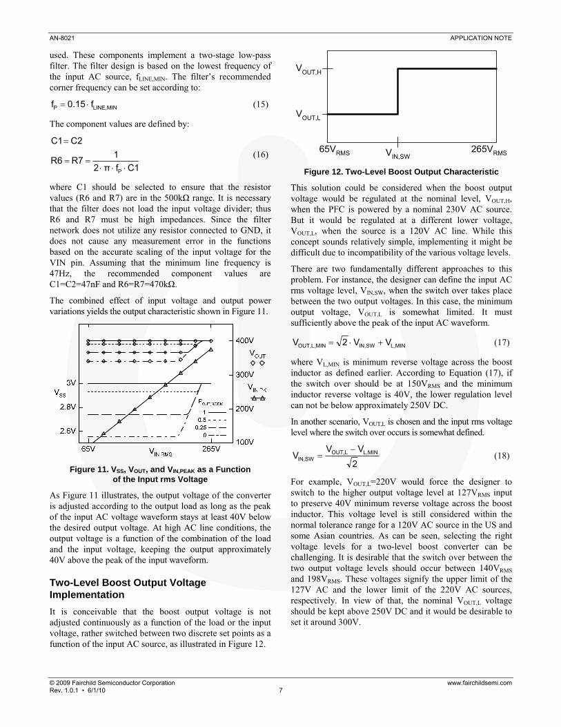
Two-Level Boost Output Voltage Implementation It is conceivable that the boost output voltage is not adjusted continuously as a function of the load or the input voltage, rather switched between two discrete set points as a function of the input AC source, as illustrated in Figure 12.
VOUT,H
VOUT,L
VIN,SW265VRMS65VRMS
Figure 12. Two-Level Boost Output Characteristic
This solution could be considered when the boost output voltage would be regulated at the nominal level, VOUT,H, when the PFC is powered by a nominal 230V AC source. But it would be regulated at a different lower voltage, VOUT,L, when the source is a 120V AC line. While this concept sounds relatively simple, implementing it might be difficult due to incompatibility of the various voltage levels.
There are two fundamentally different approaches to this problem. For instance, the designer can define the input AC rms voltage level, VIN,SW, when the switch over takes place between the two output voltages. In this case, the minimum output voltage, VOUT,L is somewhat limited. It must sufficiently above the peak of the input AC waveform.
MINL,SWIN,MINL,OUT, VV2V +⋅= (17)
where VL,MIN is minimum reverse voltage across the boost inductor as defined earlier. According to Equation (17), if the switch over should be at 150VRMS and the minimum inductor reverse voltage is 40V, the lower regulation level can not be below approximately 250V DC.
In another scenario, VOUT,L is chosen and the input rms voltage level where the switch over occurs is somewhat defined.
2VV
V MINL,LOUT,SWIN,
−= (18)
For example, VOUT,L=220V would force the designer to switch to the higher output voltage level at 127VRMS input to preserve 40V minimum reverse voltage across the boost inductor. This voltage level is still considered within the normal tolerance range for a 120V AC source in the US and some Asian countries. As can be seen, selecting the right voltage levels for a two-level boost converter can be challenging. It is desirable that the switch over between the two output voltage levels should occur between 140VRMS and 198VRMS. These voltages signify the upper limit of the 127V AC and the lower limit of the 220V AC sources, respectively. In view of that, the nominal VOUT,L voltage should be kept above 250V DC and it would be desirable to set it around 300V.
AN-8021 APPLICATION NOTE
© 2009 Fairchild Semiconductor Corporation www.fairchildsemi.com Rev. 1.0.1 • 6/1/10 8
A few other problems, which should be seriously considered when the output levels are selected, are the amplitude of the line frequency ripple voltage across the converter’s output capacitor and hold-up time requirements. The issue is that energy stored in the capacitor is proportional to the square of the output voltage. Assume that the output capacitor is calculated for 400V output and +/-20V (i.e. +/-5%) line frequency ripple at full load. At 300V output, the ripple would grow to +/-35V (or +/-12%) and, at 200V, it would reach +/-80V (equal to +/-40%). Generally, the lower the output voltage set point is, especially VOUT,L, the output capacitance of the converter must be significantly over designed to keep the line frequency ripple under control. Similarly, meeting the hold-up time requirement at a drastically lowered output voltage level imposes a severe penalty in output capacitance.
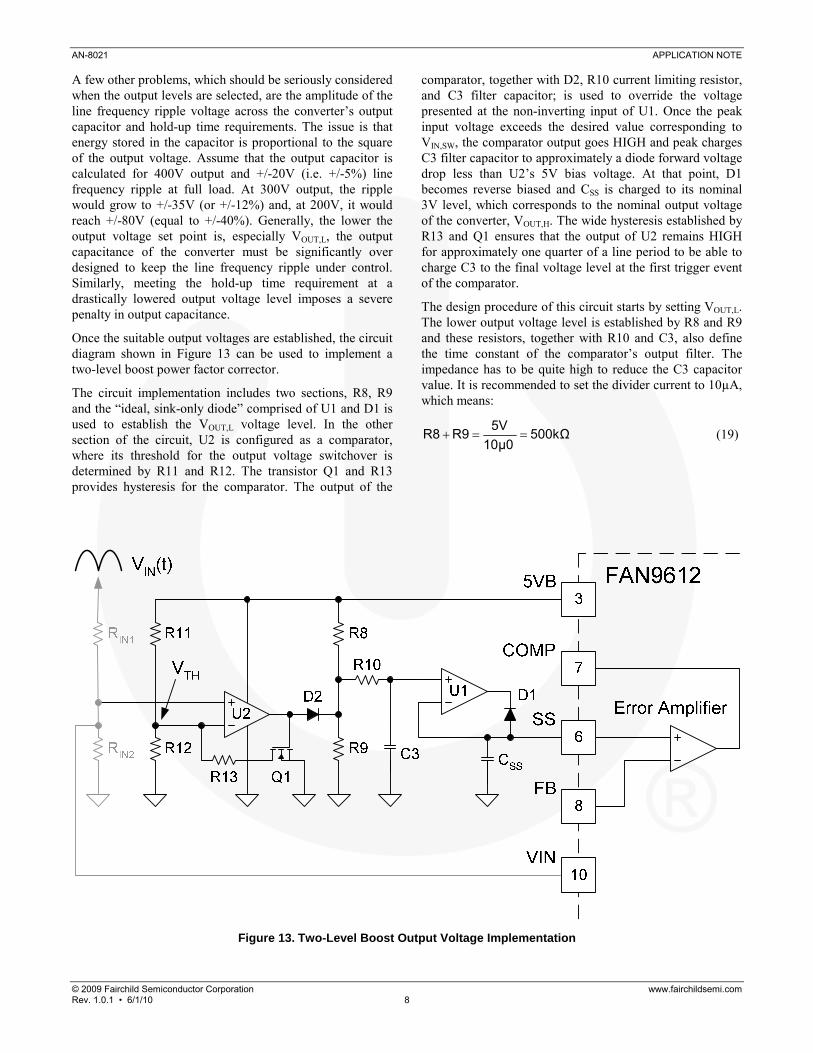
Once the suitable output voltages are established, the circuit diagram shown in Figure 13 can be used to implement a two-level boost power factor corrector.
The circuit implementation includes two sections, R8, R9 and the “ideal, sink-only diode” comprised of U1 and D1 is used to establish the VOUT,L voltage level. In the other section of the circuit, U2 is configured as a comparator, where its threshold for the output voltage switchover is determined by R11 and R12. The transistor Q1 and R13 provides hysteresis for the comparator. The output of the
comparator, together with D2, R10 current limiting resistor, and C3 filter capacitor; is used to override the voltage presented at the non-inverting input of U1. Once the peak input voltage exceeds the desired value corresponding to VIN,SW, the comparator output goes HIGH and peak charges C3 filter capacitor to approximately a diode forward voltage drop less than U2’s 5V bias voltage. At that point, D1 becomes reverse biased and CSS is charged to its nominal 3V level, which corresponds to the nominal output voltage of the converter, VOUT,H. The wide hysteresis established by R13 and Q1 ensures that the output of U2 remains HIGH for approximately one quarter of a line period to be able to charge C3 to the final voltage level at the first trigger event of the comparator.
The design procedure of this circuit starts by setting VOUT,L. The lower output voltage level is established by R8 and R9 and these resistors, together with R10 and C3, also define the time constant of the comparator’s output filter. The impedance has to be quite high to reduce the C3 capacitor value. It is recommended to set the divider current to 10µA, which means:
500kΩ10μ0
5VR9R8 ==+ (19)
Figure 13. Two-Level Boost Output Voltage Implementation
AN-8021 APPLICATION NOTE
© 2009 Fairchild Semiconductor Corporation www.fairchildsemi.com Rev. 1.0.1 • 6/1/10 9
The desired resistor values can be calculated based on the desired VOUT,L voltage level as:
( )R9R8V5VV3V
R9HOUT,
LOUT, +⋅⋅⋅
= (20)
where 3V is the nominal value of the error amplifier reference, 5V is the voltage at the 5VB pin, VOUT,H is the higher output voltage, VOUT,L is the lower output voltage level, and the sum of R8 and R9 is given by Equation (19). Assuming a total impedance of 500kΩ, R8 is given by a subtraction:
R9500kΩR8 −= (21)
For most applications, R10=5kΩ and C3=0.47µF provide sufficient filtering and current limiting for the output of U2.
The switch-over between the two output voltages occurs at a user-programmed input voltage level, VIN,SW, determined by R11 and R12. Following the method used in Equation (19) through (21), assume a 50µA divider; thus:
100kΩ50μ0
5VR12R11 ==+ (22)
( ) ( )R12R11RR5VRV2
R12IN2IN1
IN2SWIN, +⋅+⋅⋅⋅
= (23)
R12100kΩR11 −= (24)
The recommended hysteresis window is half of the comparator’s trip threshold and it can be programmed by R13 according to:
R12R11R12R11R13+⋅
= (25)
The transistor Q1 can be a small-signal NMOS component, such as 2N7002 or similar device. Its on-state impedance should be negligible compared to R13 resistance and it is chosen because its gate can be directly driven by the output of U2. Even though U2 fulfills a comparator function, it can be an operational amplifier device. The wide hysteresis window set by R13 ensures that the output changes state only once per the period of the rectified AC input waveform and the minimum pulse width is at least one quarter of that time interval. Therefore, an operational amplifier is able to switch reliably between states, allowing the user to implement U1 and U2 with a dual operational amplifier in a single package.
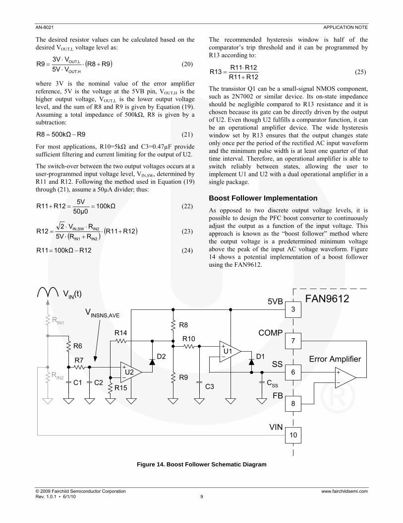
Boost Follower Implementation As opposed to two discrete output voltage levels, it is possible to design the PFC boost converter to continuously adjust the output as a function of the input voltage. This approach is known as the “boost follower” method where the output voltage is a predetermined minimum voltage above the peak of the input AC voltage waveform. Figure 14 shows a potential implementation of a boost follower using the FAN9612.
3
R9
R14
Error Amplifier
FAN9612
8
7
6
COMP
SS
FBCSS
5VB
R15
R8
R6
R7
C1 C2RIN2
RIN1
10VIN
VIN(t)
D1U1
U2
D2
VINSNS,AVE
R10
C3
Figure 14. Boost Follower Schematic Diagram
AN-8021 APPLICATION NOTE
© 2009 Fairchild Semiconductor Corporation www.fairchildsemi.com Rev. 1.0.1 • 6/1/10 10
The circuit utilizes the input voltage sense divider formed by RIN1 and RIN2, which is already present in the design providing the scaled-down version of the input voltage for the VIN pin. In addition, an averaging filter comprised of R6, R7, C1, and C2 is needed. This circuit is identical to the one introduced in Figure 10. The minimum output voltage is set by R8, R9, R10, and C3. The circuit in Figure 13 sets the lower output voltage in the two-level boost example. The interface between these two circuit blocks is provided by the gain stage comprised of U2, D2, R14, and R15. The gain stage scales the average input voltage measurement to the appropriate level to adjust the output voltage to the desired value. The ultimate reference voltage of the error amplifier is superimposed across the soft-start capacitor using the previously introduced concept of the “sink-only, ideal diode” circuit composed of U1 and D1.
Similar to the earlier design examples, a few operating parameters must be selected before the component values can be calculated. These are the minimum output voltage level of the converter, VOUT,L, and the minimum reverse voltage across the inductor during the conduction interval of the boost rectifier diode, VL,MIN. For proper selection of these parameters, refer to the important considerations outlined in the Two-Level Boost Output Voltage Implementation section.
The design procedure to set the minimum output voltage of the converter is identical to the steps of the two-level boost output voltage adjustment except the R8, R9 divider current is not critical and its current rating is increased to 50µA for better noise immunity. Note that the combination of R14 and R15 resistors is connected parallel to R9. To simplify the calculation, it is assumed that:
R15R14R9 += (26)
thus the equivalent resistance of the R9, R14, R15 network becomes half of R9:
100kΩ50μ0
5V2
R9R8 ==+ (27)
The desired resistor values can be calculated based on the desired VOUT,L voltage level as:
100kΩV5V
V3V22
R9R8V5V
V3V2R9
NOMOUT,
LOUT,
NOMOUT,
LOUT, ⋅⋅⋅⋅
=⎟⎠
⎞⎜⎝
⎛ +⋅⋅⋅⋅
=
(28)
where 3V is the nominal value of the error amplifier reference, 5V is the voltage at the 5VB pin, VOUT,nom is the nominal output voltage, VOUT,L is the lowest output voltage level, and the sum of R8 and half R9 is given by (27). Assuming a total impedance of 100kΩ, R8 is given by subtraction:
2R9100kΩR8 −= (29)
For most applications, R10=5kΩ and C3=0.47µF provide sufficient filtering and current limiting for the output of U2.
The transfer function between the input rms voltage and the VINSNS,AVE signal is given by:
IN2IN1
IN2RMSIN,AVEINSNS, RR
RV2π2V
+⋅⋅⋅= (30)
The necessary gain is set by R14 and R15. For a non-inverting gain stage, the DC gain can be expressed as:
R15R14R151KGAIN +
+= (31)
Furthermore, the gain can be determined at the critical input rms voltage when the sum of the peak line voltage and the minimum inductor reverse voltage equals the minimum output voltage level. This relationship is given by:
( ) IN2
IN2IN1
MINL,LOUT,NOMOUT,
LOUT,
GAIN
RRR
VVVV3V
2πK
+⋅
−⋅⋅
⋅
=
(32)
After equating the right-side expressions of Equations (31) and (32), substituting the relationship in Equation (26), the result can be rearranged to:
( )( ) R91
RVVV2RRV3Vπ
R15
IN2MINL,LOUT,NOMOUT,
IN2IN1LOUT, ⋅⎟⎟⎠
⎞⎜⎜⎝
⎛−
⋅−⋅⋅+⋅⋅⋅
=
(33)
Based on Equation (26), the value of R14 is:
R15R9R14 −= (34)
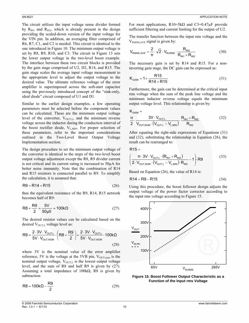
Using this procedure, the boost follower design adjusts the output voltage of the power factor corrector according to the input rms voltage according to Figure 15.
VOUT
100V
200V
300V
400V
VIN,PK
VIN,RMS265V65V
Figure 15. Boost Follower Output Characteristic as a
Function of the Input rms Voltage
AN-8021 APPLICATION NOTE
© 2009 Fairchild Semiconductor Corporation www.fairchildsemi.com Rev. 1.0.1 • 6/1/10 11
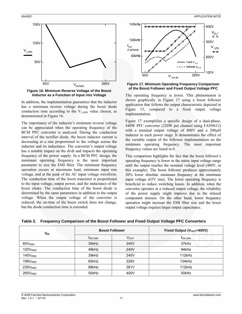
VIN,RMS265V65V
VL,MIN
50V
100V
150V
Figure 16. Minimum Reverse Voltage of the Boost
Inductor as a Function of Input rms Voltage
In addition, the implementation guarantees that the inductor has a minimum reverse voltage during the boost diode conduction time according to the VL,MIN value chosen, as demonstrated in Figure 16.
The importance of the inductor’s minimum reverse voltage can be appreciated when the operating frequency of the BCM PFC converter is analyzed. During the conduction interval of the rectifier diode, the boost inductor current is decreasing at a rate proportional to the voltage across the inductor and its inductance. The converter’s output voltage has a notable impact on the di/dt and impacts the operating frequency of the power supply. In a BCM PFC design, the minimum operating frequency is the most important parameter to size the EMI filter. The minimum frequency operation occurs at maximum load, minimum input rms voltage, and at the peak of the AC input voltage waveform. The conduction time of the boost transistor is proportional to the input voltage, output power, and the inductance of the boost choke. The conduction time of the boost diode is determined by the same parameters in addition to the output voltage. When the output voltage of the converter is reduced, the on-time of the boost switch does not change, but the diode conduction time is extended.
Figure 17. Minimum Operating Frequency Comparison of the Boost Follower and Fixed Output Voltage PFC
The operating frequency is lower. This phenomenon is shown graphically in Figure 17 using a boost follower application that follows the output characteristic depicted in Figure 15, compared to a fixed output voltage implementation.
Figure 17 exemplifies a specific design of a dual-phase, 440W PFC converter (220W per channel using FAN9612) with a nominal output voltage of 400V and a 200µH inductor in each power stage. It demonstrates the effect of the variable output of the follower implementation on the minimum operating frequency. The most important frequency values are listed in 0.
This comparison highlights the fact that the boost follower’s operating frequency is lower in the entire input voltage range until the output reaches the nominal voltage level (400V, in this example). The boost follower produces approximately 20% lower absolute minimum frequency at the minimum input voltage (65V rms). The lower operating frequency is beneficial to reduce switching losses. In addition, when the converter operates at a reduced output voltage, the reliability of the power supply might improve due to the relaxed component stresses. On the other hand, lower frequency operation might increase the EMI filter size and the lower output voltage requires larger output capacitance.
Table 2. Frequency Comparison of the Boost Follower and Fixed Output Voltage PFC Converters
VIN Boost Follower Fixed Output (VOUT=400V)
fSW,MIN VOUT fSW,MIN 65VRMS 30kHz 240V 37kHz 120VRMS 48kHz 240V 94kHz 140VRMS 39kHz 240V 112kHz 198VRMS 65kHz 328V 134kHz 230VRMS 88kHz 381V 112kHz 265VRMS 50kHz 400V 50kHz
AN-8021 APPLICATION NOTE
© 2009 Fairchild Semiconductor Corporation www.fairchildsemi.com Rev. 1.0.1 • 6/1/10 12
Furthermore, the downstream DC-DC converter must be designed for a wide input voltage range that might negatively impact its efficiency and the selection of suitable topologies.
Lastly, it is interesting to look at the operating frequency characteristics of the BCM PFC when the output power has control over the boost output voltage. In this implementation, the decreasing output power pushes the operating frequency higher. At the same time, the output voltage is adjusted lower, which has an effect of lowering the switching frequency. The combination of these two opposing trends at light load still results in higher frequency operation than at full load, but the frequency increase is reduced. The lower frequency operation, coupled with the lower switching losses due to the lower output voltage, provides a measurable improvement in efficiency at light load. Also, the output capacitor size remains relatively small and the hold-up time requirements are met under all operating conditions.
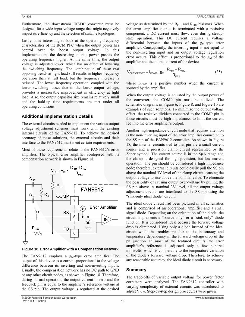
Additional Implementation Details The external circuits needed to implement the various output voltage adjustment schemes must work with the existing internal circuits of the FAN9612. To achieve the desired accuracy of these solutions, the external circuits and their interface to the FAN9612 must meet certain requirements.
Most of these requirements relate to the FAN9612’s error amplifier. The typical error amplifier configured with its compensation network is shown in Figure 18.
Figure 18. Error Amplifier with a Compensation Network
The FAN9612 employs a gM-type error amplifier. The output of this device is a current proportional to the voltage difference between its inverting and non-inverting inputs. Usually, the compensation network has no DC path to GND or any other circuit nodes, as shown in Figure 18. Therefore, during normal operation, the output current is zero and the feedback pin is equal to the amplifier’s reference voltage at the SS pin. The output voltage is regulated at the desired
voltage as determined by the RFB1 and RFB2 resistors. When the error amplifier output is terminated with a resistive component, a DC current must flow, even during steady-state operation. This DC current requires a voltage differential between the inputs of the gM-type error amplifier. Consequently, the inverting input is not equal to the non-inverting input and an output voltage regulation error occurs. This offset is proportional to the gM of the amplifier and the output current of the device.
FB2
FB2FB1MCOMPOFFSETOUT, R
RRgIV +⋅⋅= (35)
where ICOMP is a positive number when the current is sourced by the amplifier.
When the output voltage is adjusted by the output power of the converter, the COMP pin must be utilized. The schematic diagrams in Figure 6, Figure 8, and Figure 10 are examples of such solutions. To minimize the output voltage offset, the resistive dividers connected to the COMP pin in those circuits must be high impedances to limit the current fed into the error amplifier’s output.
Another high-impedance circuit node that requires attention is the non-inverting input of the error amplifier connected to the SS pin of the FAN9612 controller. As shown in Figure 18, the internal circuits tied to that pin are a small current source and a precision clamp circuit represented by the Zener symbol. The current source is in the 5µA range and the clamp is designed for high precision, but low current operation. The pin should be considered a high impedance node; therefore, external circuits could easily pull the SS pin above the nominal 3V level of the clamp circuit, causing the output voltage to rise above the nominal value. To eliminate the possibility of causing output over-voltage by pulling the SS pin above its nominal 3V level, all the output voltage adjustment circuits are interfaced to the SS pin using the “sink-only ideal diode” circuit.
The ideal diode circuit had been pictured in all schematics and is comprised of an operational amplifier and a small signal diode. Depending on the orientation of the diode, the circuit implements a “source-only” or a “sink-only” diode function. It is considered ideal because the forward voltage drop is eliminated. Using only a diode instead of the ideal circuit would be troublesome due to the inaccuracy and temperature dependency in the forward voltage drop of the pn junction. In most of the featured circuits, the error amplifier’s reference is adjusted only a few hundred millivolts, which is comparable to the temperature variation of the diode’s forward voltage drop. Therefore, to achieve any reasonable accuracy, the ideal diode circuit is necessary.
Summary The trade-offs of variable output voltage for power factor correctors were analyzed. The FAN9612 controller with varying complexity of external circuits was introduced to adjust VOUT. Step-by-step design procedures were given.

AN-8021 APPLICATION NOTE
© 2009 Fairchild Semiconductor Corporation www.fairchildsemi.com Rev. 1.0.1 • 6/1/10 13
Author Biography Laszlo Balogh is a Technical Fellow and a System Engineer at Fairchild Semiconductor. He received his MSEE degree from the Technical University of Budapest, Hungary, in 1983. After working several years designing power supplies for space, telecom, and industrial applications; he joined Unitrode, now Texas Instruments, in 1994. In 2005, Laszlo joined Fairchild Semiconductor where he works in the High-Power Solutions team. Laszlo is responsible for the
development of various analog and digital PWM controllers, power supply support integrated circuits, and their application support. In his 26-year career in power management, Laszlo has authored many conference papers and application notes, has numerous granted and pending patents, and participates in organizing and presenting the Fairchild Power Supply Design Seminar worldwide.
Related Resources Datasheet FAN9611 / FAN9612 — Interleaved Dual BCM, PFC Controller
Application Note AN-6086 — Design Consideration for Interleaved Boundary Conduction Mode PFC Using FAN9612
Application Note AN-8018 — Evaluation Board FEB279 User Guide , 400W Evaluation Board using FAN9612
Fairchild Power Seminar 2008-2009 Paper — Understanding Interleaved Boundary Conduction Mode PFC Converters
DISCLAIMER FAIRCHILD SEMICONDUCTOR RESERVES THE RIGHT TO MAKE CHANGES WITHOUT FURTHER NOTICE TO ANY PRODUCTS HEREIN TO IMPROVE RELIABILITY, FUNCTION, OR DESIGN. FAIRCHILD DOES NOT ASSUME ANY LIABILITY ARISING OUT OF THE APPLICATION OR USE OF ANY PRODUCT OR CIRCUIT DESCRIBED HEREIN; NEITHER DOES IT CONVEY ANY LICENSE UNDER ITS PATENT RIGHTS, NOR THE RIGHTS OF OTHERS. LIFE SUPPORT POLICY FAIRCHILD’S PRODUCTS ARE NOT AUTHORIZED FOR USE AS CRITICAL COMPONENTS IN LIFE SUPPORT DEVICES OR SYSTEMS WITHOUT THE EXPRESS WRITTEN APPROVAL OF THE PRESIDENT OF FAIRCHILD SEMICONDUCTOR CORPORATION. As used herein: 1. Life support devices or systems are devices or systems
which, (a) are intended for surgical implant into the body, or (b) support or sustain life, or (c) whose failure to perform when properly used in accordance with instructions for use provided in the labeling, can be reasonably expected to result in significant injury to the user.
2. A critical component is any component of a life support device or system whose failure to perform can be reasonably expected to cause the failure of the life support device or system, or to affect its safety or effectiveness.
www.onsemi.com1
ON Semiconductor and are trademarks of Semiconductor Components Industries, LLC dba ON Semiconductor or its subsidiaries in the United States and/or other countries.ON Semiconductor owns the rights to a number of patents, trademarks, copyrights, trade secrets, and other intellectual property. A listing of ON Semiconductor’s product/patentcoverage may be accessed at www.onsemi.com/site/pdf/Patent−Marking.pdf. ON Semiconductor reserves the right to make changes without further notice to any products herein.ON Semiconductor makes no warranty, representation or guarantee regarding the suitability of its products for any particular purpose, nor does ON Semiconductor assume any liabilityarising out of the application or use of any product or circuit, and specifically disclaims any and all liability, including without limitation special, consequential or incidental damages.Buyer is responsible for its products and applications using ON Semiconductor products, including compliance with all laws, regulations and safety requirements or standards,regardless of any support or applications information provided by ON Semiconductor. “Typical” parameters which may be provided in ON Semiconductor data sheets and/orspecifications can and do vary in different applications and actual performance may vary over time. All operating parameters, including “Typicals” must be validated for each customerapplication by customer’s technical experts. ON Semiconductor does not convey any license under its patent rights nor the rights of others. ON Semiconductor products are notdesigned, intended, or authorized for use as a critical component in life support systems or any FDA Class 3 medical devices or medical devices with a same or similar classificationin a foreign jurisdiction or any devices intended for implantation in the human body. Should Buyer purchase or use ON Semiconductor products for any such unintended or unauthorizedapplication, Buyer shall indemnify and hold ON Semiconductor and its officers, employees, subsidiaries, affiliates, and distributors harmless against all claims, costs, damages, andexpenses, and reasonable attorney fees arising out of, directly or indirectly, any claim of personal injury or death associated with such unintended or unauthorized use, even if suchclaim alleges that ON Semiconductor was negligent regarding the design or manufacture of the part. ON Semiconductor is an Equal Opportunity/Affirmative Action Employer. Thisliterature is subject to all applicable copyright laws and is not for resale in any manner.
PUBLICATION ORDERING INFORMATIONN. American Technical Support: 800−282−9855 Toll FreeUSA/Canada
Europe, Middle East and Africa Technical Support:Phone: 421 33 790 2910
Japan Customer Focus CenterPhone: 81−3−5817−1050
www.onsemi.com
LITERATURE FULFILLMENT:Literature Distribution Center for ON Semiconductor19521 E. 32nd Pkwy, Aurora, Colorado 80011 USAPhone: 303−675−2175 or 800−344−3860 Toll Free USA/CanadaFax: 303−675−2176 or 800−344−3867 Toll Free USA/CanadaEmail: [email protected]
ON Semiconductor Website: www.onsemi.com
Order Literature: http://www.onsemi.com/orderlit
For additional information, please contact your localSales Representative
© Semiconductor Components Industries, LLC


![Proxima Centaur™ EF Control Unit - Caldertech...Input Frequency 40 - 60Hz Input Current [Max. A] 16A Input Power 3kW Output Voltage [Vac RMS] 8 - 48v Output Current [Continuous](https://img.pdfslide.us/doc/110x75/6132fe13dfd10f4dd73acd61/proxima-centaura-ef-control-unit-caldertech-input-frequency-40-60hz-input.jpg)