Embed Size (px)
Citation preview
AN 706: Mapping HPS IP Peripheral Signals to theFPGA Interface
2018.05.07
AN-706 Subscribe Send Feedback
The Altera Cyclone® V and Arria® V SoC device families integrate an Arm* Cortex*-A9-based hardprocessor system (HPS) consisting of processor, peripherals, and memory interface with the FPGA fabricusing a high-bandwidth interconnect backbone. The Cyclone V HPS interface provides up to 67 I/O pinsto share with multiple peripherals through sets of configurable multiplexers. TheArria V HPS interfaceprovides up to 71 I/O pins.
This application note describes the steps required to route an HPS peripheral through the FPGA interfaceusing Platform Designer (Standard) and Intel® Quartus® Prime Standard Edition software. A simpledesign example is included to demonstrate exporting HPS EMAC0 and I2C0 peripheral signals to theFPGA interface using a Cyclone V SoC Development Kit.
Cyclone V and Arria V HPS Peripherals That Support Routing to the FPGAThe following types of Cyclone V and Arria V HPS peripherals are capable of routing to the FPGA fabric:
• Ethernet Media Access Controller (EMAC)• Quad Serial Peripheral Interface (QSPI)• Secure Digital/Multimedia Card (SD/MMC)• Serial Peripheral Interface (SPI)• Universal Asynchronous Receiver/Transmitter (UART)• Inter-Integrated Circuit (I2C)• Controller Area Network (CAN)(1)
In many cases, routing the HPS IP signals to the FPGA external interface allows more signals to beexposed.
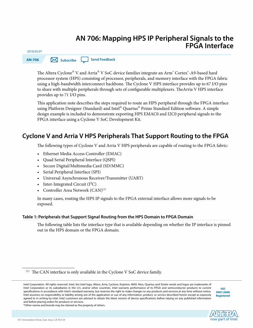
Table 1: Peripherals that Support Signal Routing from the HPS Domain to FPGA Domain
The following table lists the interface type that is available depending on whether the IP interface is pinnedout in the HPS domain or the FPGA domain.
(1) The CAN interface is only available in the Cyclone V SoC device family.
Intel Corporation. All rights reserved. Intel, the Intel logo, Altera, Arria, Cyclone, Enpirion, MAX, Nios, Quartus and Stratix words and logos are trademarks ofIntel Corporation or its subsidiaries in the U.S. and/or other countries. Intel warrants performance of its FPGA and semiconductor products to currentspecifications in accordance with Intel's standard warranty, but reserves the right to make changes to any products and services at any time without notice.Intel assumes no responsibility or liability arising out of the application or use of any information, product, or service described herein except as expresslyagreed to in writing by Intel. Intel customers are advised to obtain the latest version of device specifications before relying on any published informationand before placing orders for products or services.*Other names and brands may be claimed as the property of others.
ISO9001:2008Registered
www.altera.com101 Innovation Drive, San Jose, CA 95134
Peripherals Interface Description
HPS Domain FPGA Domain
EMAC RGMII Interface GMII Interface
QSPI Standard QSPI interface with fourslave select signals
Standard QSPI interface withfour slave select signals achievedby connecting exported signalsto bidirectional buffers
SD/MMC Standard SD/MMC interface withup to 8-bit data bus
Standard SD/MMC interface,including:
• Up to 8-bit data bus• Card detect interface• Card interrupt• Voltage switching• Power enable• Reset (2)
SPI Master MOSI/MISO SPI interface configu‐rable to single or dual slaves
MOSI/MISO SPI interface withoutput enables that support up tofour slaves; interface achieved byconnecting exported signals tobidirectional buffers
SPI Slave MOSI/MISO SPI interface configu‐rable to single or dual slaves
MOSI/MISO SPI interface withoutput enables that support up tofour slaves; interface achieved byconnecting exported signals tobidirectional buffers
UART Standard UART interface with flowcontrol signals
Standard UART interface withflow control signals, includingDTR and DSR; status and twouser-defined output signals arealso available
I2C Standard I2C interface Standard I2C interface achievedby connecting exported signalsto a bidirectional buffer
CAN(3) Standard CAN interface Standard CAN interface
(2) The SD/MMC controller does not directly support reset, voltage switching, card interrupts, power enableor write protect functions. However, you can connect these signals to general-purpose I/Os (GPIOs).
(3) The CAN interface is only available in the Cyclone V SoC device family.
2 Cyclone V and Arria V HPS Peripherals That Support Routing to the FPGAAN-706
2018.05.07
Altera Corporation AN 706: Mapping HPS IP Peripheral Signals to the FPGA Interface
Send Feedback
Refer to the following chapters of the Cyclone V Hard Processor System Technical Reference Manual fordescriptions of each peripheral signal interface:
Related Information
• General-Purpose I/O Interface• SD/MMC Controller• Ethernet Media Access Controller• Quad SPI Flash Controller• SPI Controller• UART Controller• I2C Controller• CAN Controller
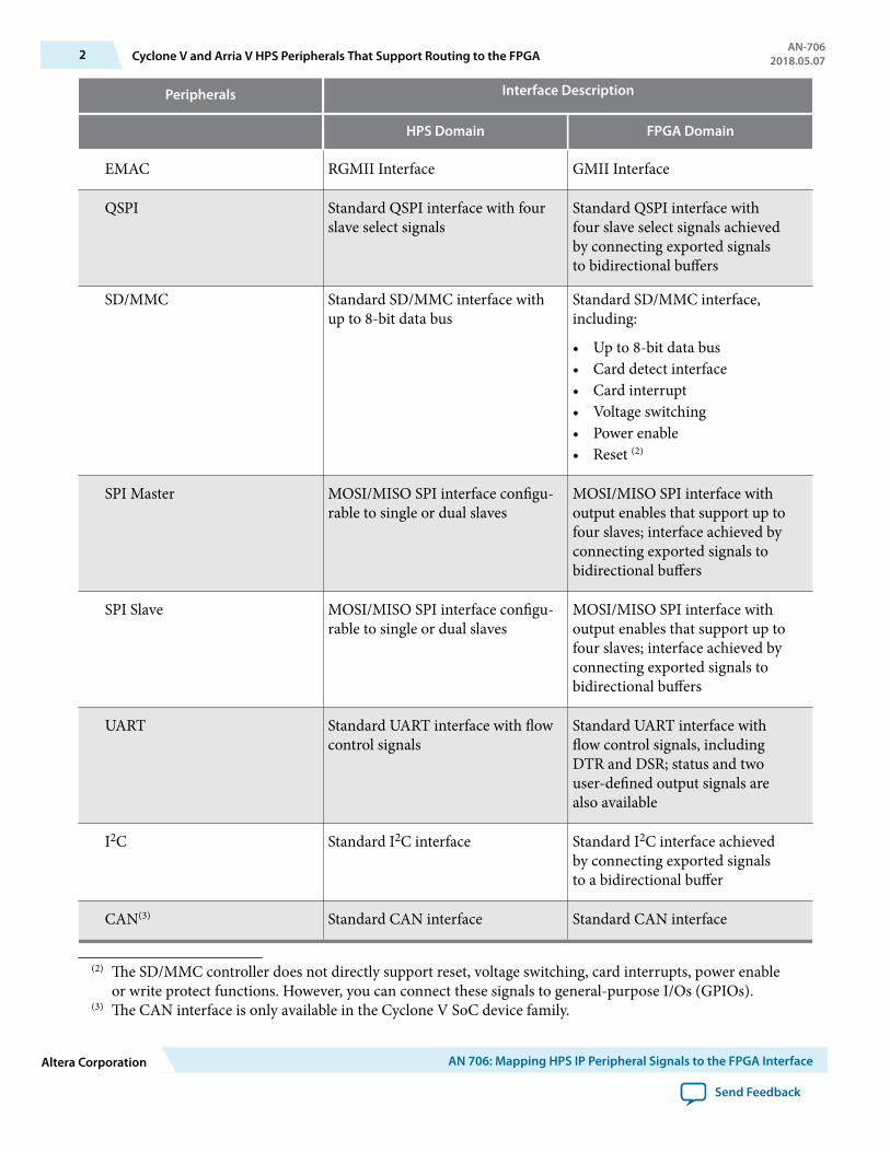
Design Example: Cyclone V HPS IP Interface to FPGAThis design example, based on the Golden System Reference Design (GSRD), uses the Cyclone V SoCdevelopment kit resources to demonstrate routing the Cyclone V HPS EMAC0 and I2C0 peripheral signalsto the FPGA interface.
The Cyclone V HPS component provides up to two EMAC peripherals, which support 10/100/1000 Mbpsoperation. The Cyclone V SoC Development board is populated with a Micrel KSZ9021RN RGMII PHYthat interfaces to the HPS domain and a Renesas uPD60620A MII Dual Port PHY that interfaces to theFPGA domain. The HPS and FPGA also share a common I2C bus to various on-board I2C slaves.
Figure 1: High-level Routing Layout of Cyclone V SoC Board Design Example
FPGA Domain
Altera 5CSXFC6D6F31C6
AXIBridge
System Design
SubsystemCortex-A9 MPU
Renesas PHY
L3 Interconnect
I2C Slaves
EMAC0
I2C0
Cyclone V SoC Development Board
GMII Signals
I2C Signals
10/100 Ethernet
The following sections provide the necessary information to route the HPS peripherals to the FPGAinterface, such as:
1. Prerequisites on page 4
AN-7062018.05.07 Design Example: Cyclone V HPS IP Interface to FPGA 3
AN 706: Mapping HPS IP Peripheral Signals to the FPGA Interface Altera Corporation
Send Feedback
2. Getting Started on page 53. Generating the Initial HDL in Platform Designer (Standard) on page 54. Top Level Routing on page 95. Timing Constraint Configuration on page 116. Adding Pin Assignments in Intel Quartus Prime Standard Edition on page 117. Hardware Programming File Compilation and Generation on page 138. SD Card Image Updates on page 149. Board Setup and Booting Linux from the SD Card on page 15
PrerequisitesThis design example is based on the Cyclone V GSRD and tested with Intel Quartus Prime StandardEdition version 14.0. Refer to the links listed below and review the recommended material before startingwith this design example.
Related Information
• Cyclone V SoC Development KitRefer to this link for Cyclone V SoC Development Kit documentation and installation files.
• Golden System Reference Design User's ManualRefer to this document and step through the Getting Started Guides, Prerequisites, and the GHRDOverview. In addition, review the Development Flow Overview.
Hardware Requirements
The hardware required for this design example is:
• Cyclone V SoC Development Kit• RJ45 Ethernet cable• SD/MMC card preloaded with default GSRD image
Software Requirements
The software required for this design example is:
• Intel Quartus Prime Standard Edition 14.0 and above• SoC EDS 14.0 and above• Factory default hardware template cv_soc_devkit_ghrd in SoC EDS 14.0
Design example files are provided in the AN 706 design example link and are listed in the table below.
Table 2: Required Software Files
File Name Description
ghrd_top.v Top level RTL file
soc_system_timing.sdc Timing constraint file
an706_de_pin_assignment.tcl Pin assignment script file
4 PrerequisitesAN-706
2018.05.07
Altera Corporation AN 706: Mapping HPS IP Peripheral Signals to the FPGA Interface
Send Feedback
File Name Description
preloader-mkpimage.bin Generated preloader binary targeted to this project
u-boot.img Modified u-boot image for EMAC0
socfpga.dtb Modified device tree for EMAC0 and I2C0
Getting Started1. Make a copy of the Cyclone V Golden Hardware Reference Design (GHRD) from your Cyclone
V SoC Development Kit installation location or download the latest Cyclone V GHRD design examplefrom the Rocketboards website to your project location.
2. Download the AN 706 design files (an706-design-files.zip) provided.3. Open the GHRD project within the Intel Quartus Prime Standard Edition software.
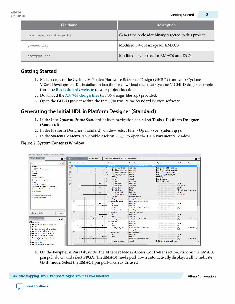
Generating the Initial HDL in Platform Designer (Standard)1. In the Intel Quartus Prime Standard Edition navigation bar, select Tools > Platform Designer
(Standard).2. In the Platform Designer (Standard) window, select File > Open > soc_system.qsys.3. In the System Contents tab, double click on hps_0 to open the HPS Parameters window.
Figure 2: System Contents Window
4. On the Peripheral Pins tab, under the Ethernet Media Access Controller section, click on the EMAC0pin pull-down and select FPGA. The EMAC0 mode pull-down automatically displays Full to indicateGMII mode. Select the EMAC1 pin pull-down as Unused.
AN-7062018.05.07 Getting Started 5
AN 706: Mapping HPS IP Peripheral Signals to the FPGA Interface Altera Corporation
Send Feedback
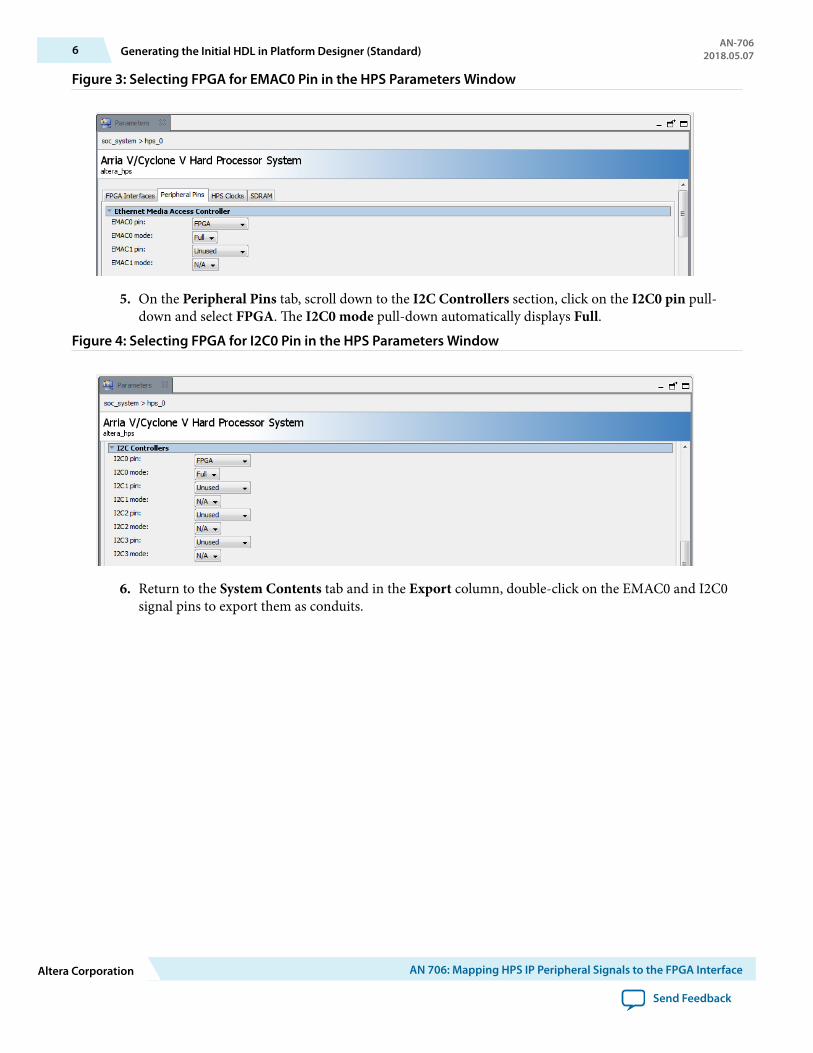
Figure 3: Selecting FPGA for EMAC0 Pin in the HPS Parameters Window
5. On the Peripheral Pins tab, scroll down to the I2C Controllers section, click on the I2C0 pin pull-down and select FPGA. The I2C0 mode pull-down automatically displays Full.
Figure 4: Selecting FPGA for I2C0 Pin in the HPS Parameters Window
6. Return to the System Contents tab and in the Export column, double-click on the EMAC0 and I2C0signal pins to export them as conduits.
6 Generating the Initial HDL in Platform Designer (Standard)AN-706
2018.05.07
Altera Corporation AN 706: Mapping HPS IP Peripheral Signals to the FPGA Interface
Send Feedback
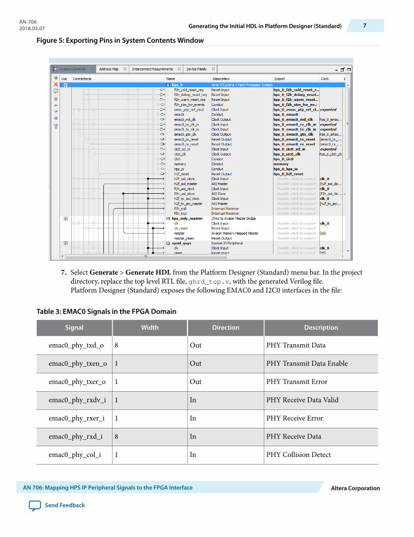
Figure 5: Exporting Pins in System Contents Window
7. Select Generate > Generate HDL from the Platform Designer (Standard) menu bar. In the projectdirectory, replace the top level RTL file, ghrd_top.v, with the generated Verilog file.Platform Designer (Standard) exposes the following EMAC0 and I2C0 interfaces in the file:
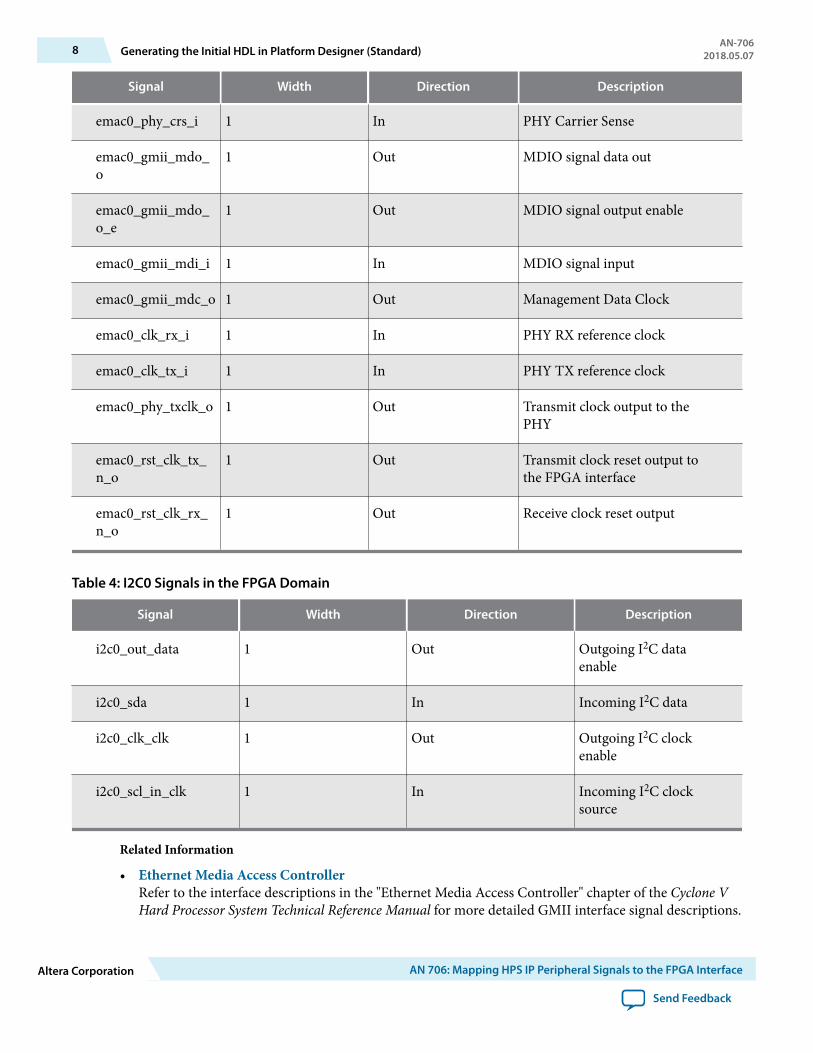
Table 3: EMAC0 Signals in the FPGA Domain
Signal Width Direction Description
emac0_phy_txd_o 8 Out PHY Transmit Data
emac0_phy_txen_o 1 Out PHY Transmit Data Enable
emac0_phy_txer_o 1 Out PHY Transmit Error
emac0_phy_rxdv_i 1 In PHY Receive Data Valid
emac0_phy_rxer_i 1 In PHY Receive Error
emac0_phy_rxd_i 8 In PHY Receive Data
emac0_phy_col_i 1 In PHY Collision Detect
AN-7062018.05.07 Generating the Initial HDL in Platform Designer (Standard) 7
AN 706: Mapping HPS IP Peripheral Signals to the FPGA Interface Altera Corporation
Send Feedback
Signal Width Direction Description
emac0_phy_crs_i 1 In PHY Carrier Sense
emac0_gmii_mdo_o
1 Out MDIO signal data out
emac0_gmii_mdo_o_e
1 Out MDIO signal output enable
emac0_gmii_mdi_i 1 In MDIO signal input
emac0_gmii_mdc_o 1 Out Management Data Clock
emac0_clk_rx_i 1 In PHY RX reference clock
emac0_clk_tx_i 1 In PHY TX reference clock
emac0_phy_txclk_o 1 Out Transmit clock output to thePHY
emac0_rst_clk_tx_n_o
1 Out Transmit clock reset output tothe FPGA interface
emac0_rst_clk_rx_n_o
1 Out Receive clock reset output
Table 4: I2C0 Signals in the FPGA Domain
Signal Width Direction Description
i2c0_out_data 1 Out Outgoing I2C dataenable
i2c0_sda 1 In Incoming I2C data
i2c0_clk_clk 1 Out Outgoing I2C clockenable
i2c0_scl_in_clk 1 In Incoming I2C clocksource
Related Information
• Ethernet Media Access ControllerRefer to the interface descriptions in the "Ethernet Media Access Controller" chapter of the Cyclone VHard Processor System Technical Reference Manual for more detailed GMII interface signal descriptions.
8 Generating the Initial HDL in Platform Designer (Standard)AN-706
2018.05.07
Altera Corporation AN 706: Mapping HPS IP Peripheral Signals to the FPGA Interface
Send Feedback
• I2C ControllerRefer to the interface descriptions in the "I2C Controller" chapter of the Cyclone V Hard ProcessorSystem Technical Reference Manual for more detailed I2C interface signal descriptions.
Top Level RoutingThe top level RTL file defines the pin connections from the Cyclone V HPS EMAC0 to the Renesas MIIPHY on the Cyclone V SoC development board.
Note: Because MII is a 4-bit data width protocol, connect only the lower 4-bits, emac0_phy_txd_o[3:0]and emac0_phy_rxd_i[3:0], of EMAC0's RX and TX interface from the FPGA.
AN-7062018.05.07 Top Level Routing 9
AN 706: Mapping HPS IP Peripheral Signals to the FPGA Interface Altera Corporation
Send Feedback
Figure 6: Routing of the EMAC0 FPGA Interface to the On-board MII PHY
gmii_mdo_o_e
gmii_mdo_o
gmii_mdi_i
gmii_mdc_o
phy_txd_o[3]
phy_txen_o
phy_txer_o
phy_rxd_i[0]
phy_rxdv_i
phy_rxer_i
clk_rx_i
clk_tx_i
phy_txclk_o / gtx_clk
rst_clk_tx_n_o
rst_clk_rx_n_o
phy_col_i
phy_crs_i
MDIO
MDC
P0_TXD[3]
P0_TXEN
P0_TXER
P0_RXD[0]
P0_RXDV
P0_RXER
P0_RXCLK
P0_TXCLK
P0_CRS
P0_COL
HPS-to-FPGA Signal Interface PHY Signal Interface
phy_txd_o[2] P0_TXD[2]
phy_txd_o[1] P0_TXD[1]
phy_txd_o[0] P0_TXD[0]
phy_rxd_i[3] P0_RXD[3]
phy_rxd_i[2] P0_RXD[2]
phy_rxd_i[1] P0_RXD[1]
HPS I2C0 is routed through the FPGA interface and acts as a master to various on-board I2C slaves:
• Two Octal Digital Power Supply Managers with EEPROM• LCD• RTC• EEPROM
Note: A bi-directional buffer, ALT_IOBUF, must be added in the design to connect the I2C signals to anexternal open drain IO. The buffer can be included by instantiating ALT_IOBUF in ghrd_top.v.
10 Top Level RoutingAN-706
2018.05.07
Altera Corporation AN 706: Mapping HPS IP Peripheral Signals to the FPGA Interface
Send Feedback
The following Verilog code shows the ALT_IOBUF instantiation for an I2C interface implemented throughthe FPGA:
ALT_IOBUF scl_iobuf (.i(1'b0), .oe(scl_o_e), .o(scl_o), .io(fpga_i2c_scl)); //declared bi-directional buffer for sclALT_IOBUF sda_iobuf (.i(1'b0), .oe(sda_o_e), .o(sda_o), .io(fpga_i2c_sda)); //declared bi-directional buffer for sda
Related InformationALT_IOBUF PrimitiveRefer to the ALT_IOBUF primitive information for more information.
Timing Constraint ConfigurationReplace the soc_system_timing.sdc file in your project directory with the soc_system_timing.sdc file provided in the project folder. This new file is customized for the EMAC0 and I2C0interface being tested on the Cyclone V SoC development board.
Adding Pin Assignments in Intel Quartus Prime Standard Edition1. Copy an706_de_pin_assignment.tcl from the AN 706 design files into your project directory.2. In the Intel Quartus Prime Standard Edition menu bar, select Tools > Tcl Scripts3. In the Tcl Scripts window, choose an706_de_pin_assignment.tcl and select Run.
AN-7062018.05.07 Timing Constraint Configuration 11
AN 706: Mapping HPS IP Peripheral Signals to the FPGA Interface Altera Corporation
Send Feedback
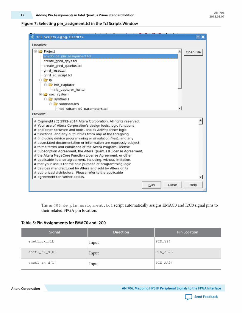
Figure 7: Selecting pin_assigment.tcl in the Tcl Scripts Window
The an706_de_pin_assignment.tcl script automatically assigns EMAC0 and I2C0 signal pins totheir related FPGA pin location.
Table 5: Pin Assignments for EMAC0 and I2C0
Signal Direction Pin Location
enet1_rx_clk Input PIN_Y24
enet1_rx_d[0] Input PIN_AB23
enet1_rx_d[1] Input PIN_AA24
12 Adding Pin Assignments in Intel Quartus Prime Standard EditionAN-706
2018.05.07
Altera Corporation AN 706: Mapping HPS IP Peripheral Signals to the FPGA Interface
Send Feedback
Signal Direction Pin Location
enet1_rx_d[2] Input PIN_AB25
enet1_rx_d[3] Input PIN_AE27
enet1_rx_dv Input PIN_Y23
enet1_rx_error Input PIN_AE28
enet1_tx_clk_fb Input PIN_W25
enet1_tx_d[0] Output PIN_W20
enet1_tx_d[1] Output PIN_Y21
enet1_tx_d[2] Output PIN_AA25
enet1_tx_d[3] Output PIN_AB26
enet1_tx_en Output PIN_AB22
enet1_tx_error Output PIN_AG5
enet_dual_resetn Output PIN_AJ1
enet_fpga_mdc Output PIN_H12
enet_fpga_mdio Bidirectional PIN_H13
fpga_i2c_scl Bidirectional PIN_G7
fpga_i2c_sda Bidirectional PIN_F6
Hardware Programming File Compilation and GenerationAfter the Platform Designer (Standard) system is set up, the top level RTL file updated, the related signalpin location assigned and timing constrained, the design can be compiled and the SOF programming filegenerated.
In the Intel Quartus Prime Standard Edition software navigation bar, select Processing > Start Compila‐tion to generate the SOF programming file.
AN-7062018.05.07 Hardware Programming File Compilation and Generation 13
AN 706: Mapping HPS IP Peripheral Signals to the FPGA Interface Altera Corporation
Send Feedback
SD Card Image UpdatesUpdate the default SD card image with the generated preloader binary, u-boot image file and DTB filefollowing the steps described below:
1. With your Linux machine, prepare the SD card by following the information in GSRD-Booting LinuxUsing Prebuilt SD Card Image. Untar the sd_image.bin.tar.gz file and program the image file,sd_image.bin into the SD card.
2. Replace the preloader-mkpimage.bin, u-boot.img and socfpga.dtb in the SD card.
Note: Information provided regarding SD card changes, preloader and Linux software file changes andpreloader generation are applicable to this reference design only.
Preloader Generation
Because this design example modifies the default GHRD Platform Designer (Standard) file, it is essentialto re-generate the preloader with the preloader generator.
Related InformationGSRD - Generating and Compiling the PreloaderRefer to this location for information on how to generate and compile the preloader.
U-boot Setup
Go to file location u-boot-socfpga/include/configs/socfpga_cyclone.h. The EMAC0parameters associated with the interface speed must be configured to MII in the socfpga_cyclone.hfile in the u-boot source. Change the #define for CONFIG_EMAC_BASE and CONFIG_PHY_INTERFACE_MODEto the following:
#define CONFIG_EMAC_BASE CONFIG_EMAC0_BASE#define CONFIG_PHY_INTERFACE_MODE SOCFPGA_PHYSEL_ENUM_MII
Related InformationPreloader and U-Boot CustomizationRefer to this location for information on how to customize u-boot.
14 SD Card Image UpdatesAN-706
2018.05.07
Altera Corporation AN 706: Mapping HPS IP Peripheral Signals to the FPGA Interface
Send Feedback
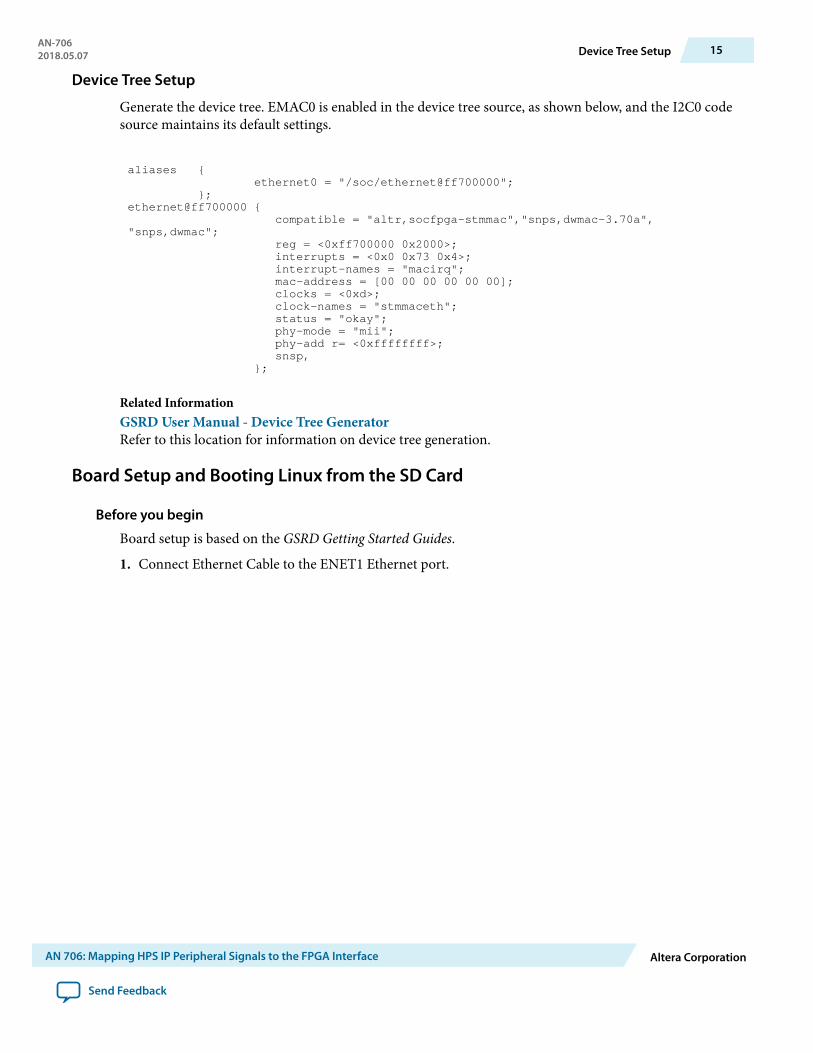
Device Tree Setup
Generate the device tree. EMAC0 is enabled in the device tree source, as shown below, and the I2C0 codesource maintains its default settings.
aliases { ethernet0 = "/soc/ethernet@ff700000"; }; ethernet@ff700000 { compatible = "altr,socfpga-stmmac","snps,dwmac-3.70a", "snps,dwmac"; reg = <0xff700000 0x2000>; interrupts = <0x0 0x73 0x4>; interrupt-names = "macirq"; mac-address = [00 00 00 00 00 00]; clocks = <0xd>; clock-names = "stmmaceth"; status = "okay"; phy-mode = "mii"; phy-add r= <0xffffffff>; snsp, };
Related InformationGSRD User Manual - Device Tree GeneratorRefer to this location for information on device tree generation.
Board Setup and Booting Linux from the SD Card
Before you begin
Board setup is based on the GSRD Getting Started Guides.
1. Connect Ethernet Cable to the ENET1 Ethernet port.
AN-7062018.05.07 Device Tree Setup 15
AN 706: Mapping HPS IP Peripheral Signals to the FPGA Interface Altera Corporation
Send Feedback
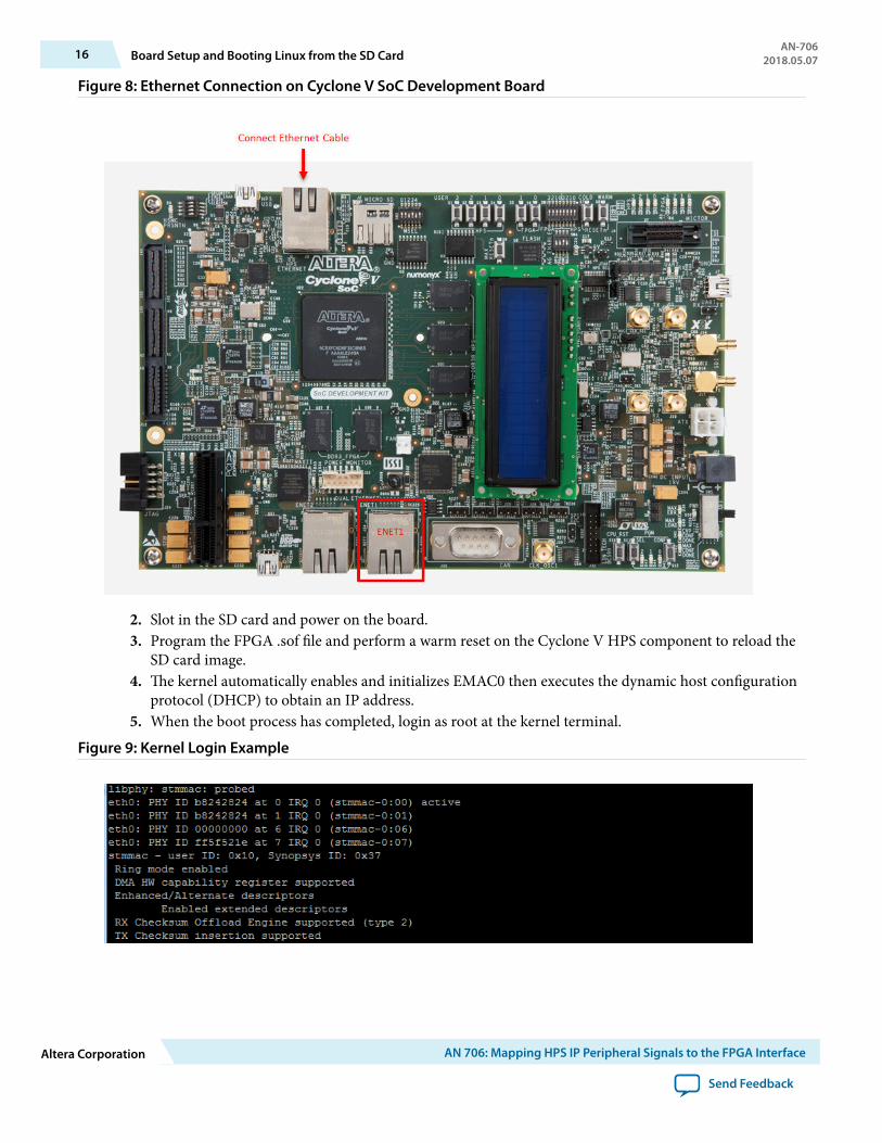
Figure 8: Ethernet Connection on Cyclone V SoC Development Board
2. Slot in the SD card and power on the board.3. Program the FPGA .sof file and perform a warm reset on the Cyclone V HPS component to reload the
SD card image.4. The kernel automatically enables and initializes EMAC0 then executes the dynamic host configuration
protocol (DHCP) to obtain an IP address.5. When the boot process has completed, login as root at the kernel terminal.
Figure 9: Kernel Login Example
16 Board Setup and Booting Linux from the SD CardAN-706
2018.05.07
Altera Corporation AN 706: Mapping HPS IP Peripheral Signals to the FPGA Interface
Send Feedback
Related Information
• GSRD User's Manual - Getting Started GuidesRefer to this location for information on board setup in the GSRD User's Manual - Getting StartedGuides.
• GSRD - SD CardRefer to this location for information on updating the SD Card.
Sample Application ExampleThe default kernel image contains many useful commands and built-in tools, such as ethtools andmii-tools. Some examples are illustrated in this section.
EMAC TestExamples of commands that can be executed on EMAC0 are:
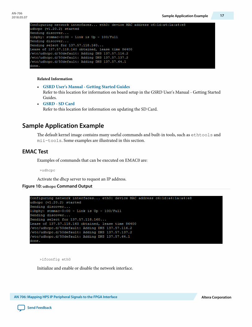
>udhcpc
Activate the dhcp server to request an IP address.Figure 10: udhcpc Command Output
>ifconfig eth0
Initialize and enable or disable the network interface.
AN-7062018.05.07 Sample Application Example 17
AN 706: Mapping HPS IP Peripheral Signals to the FPGA Interface Altera Corporation
Send Feedback
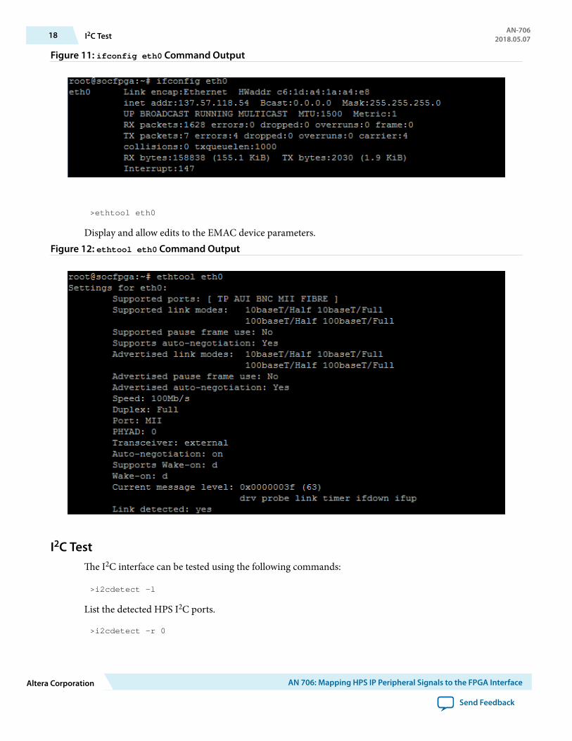
Figure 11: ifconfig eth0 Command Output
>ethtool eth0
Display and allow edits to the EMAC device parameters.Figure 12: ethtool eth0 Command Output
I2C TestThe I2C interface can be tested using the following commands:
>i2cdetect -l
List the detected HPS I2C ports.
>i2cdetect -r 0
18 I2C TestAN-706
2018.05.07
Altera Corporation AN 706: Mapping HPS IP Peripheral Signals to the FPGA Interface
Send Feedback
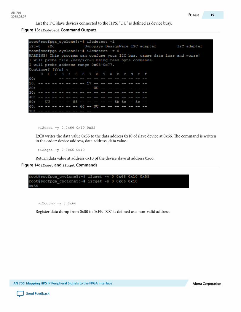
List the I2C slave devices connected to the HPS. "UU" is defined as device busy.Figure 13: i2cdetect Command Outputs
>i2cset -y 0 0x66 0x10 0x55
I2C0 writes the data value 0x55 to the data address 0x10 of slave device at 0x66. The command is writtenin the order: device address, data address, data value.
>i2cget -y 0 0x66 0x10
Return data value at address 0x10 of the device slave at address 0x66.Figure 14: i2cset and i2cget Commands
>i2cdump -y 0 0x66
Register data dump from 0x00 to 0xFF. "XX" is defined as a non-valid address.
AN-7062018.05.07 I2C Test 19
AN 706: Mapping HPS IP Peripheral Signals to the FPGA Interface Altera Corporation
Send Feedback
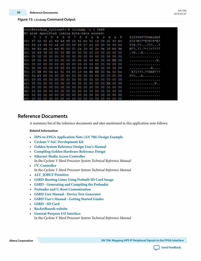
Figure 15: i2cdump Command Output
Reference DocumentsA summary list of the reference documents and sites mentioned in this application note follows:
Related Information
• HPS-to-FPGA Application Note (AN 706) Design Example• Cyclone V SoC Development Kit• Golden System Reference Design User's Manual• Compiling Golden Hardware Reference Design• Ethernet Media Access Controller
In the Cyclone V Hard Processor System Technical Reference Manual• I2C Controller
In the Cyclone V Hard Processor System Technical Reference Manual• ALT_IOBUF Primitive• GSRD-Booting Linux Using Prebuilt SD Card Image• GSRD - Generating and Compiling the Preloader• Preloader and U-Boot Customization• GSRD User Manual - Device Tree Generator• GSRD User's Manual - Getting Started Guides• GSRD - SD Card• RocketBoards website• General-Purpose I/O Interface
In the Cyclone V Hard Processor System Technical Reference Manual
20 Reference DocumentsAN-706
2018.05.07
Altera Corporation AN 706: Mapping HPS IP Peripheral Signals to the FPGA Interface
Send Feedback
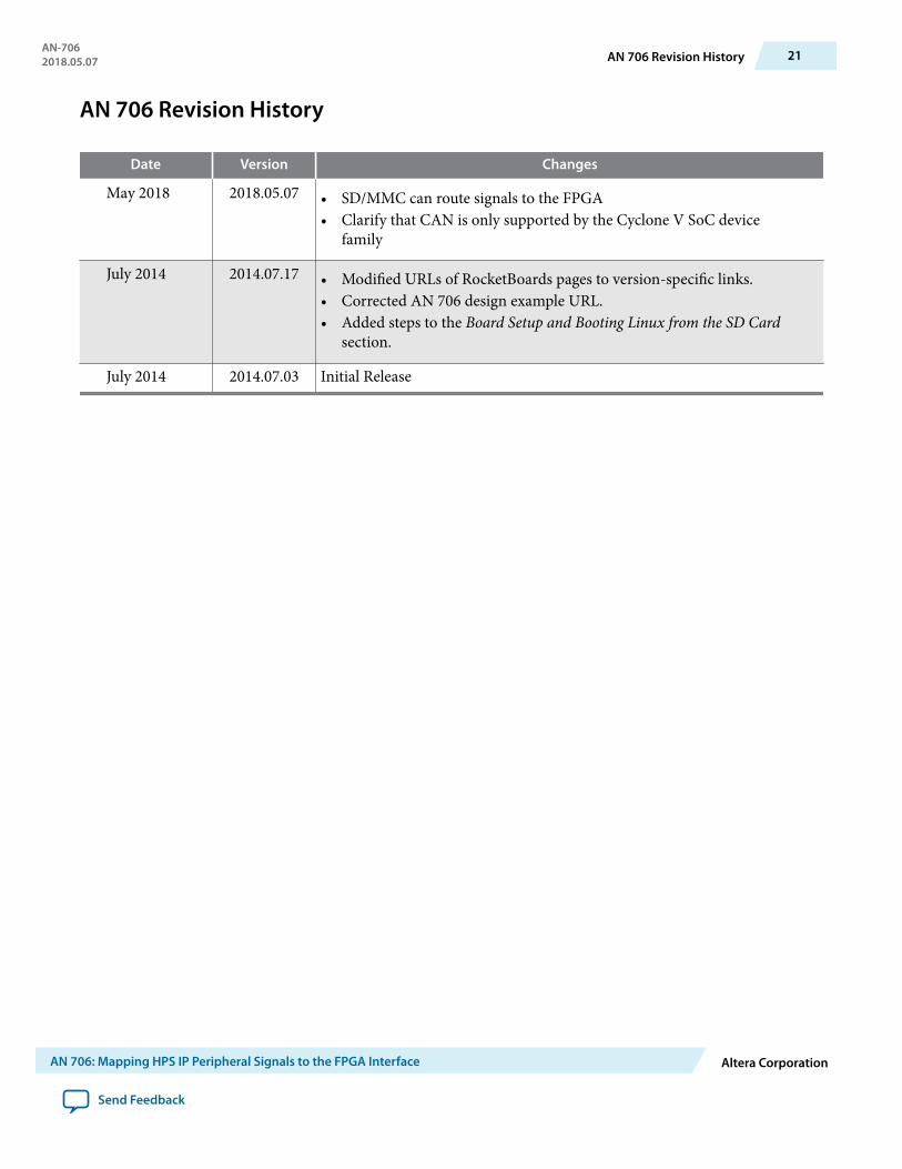
AN 706 Revision History
Date Version Changes
May 2018 2018.05.07 • SD/MMC can route signals to the FPGA• Clarify that CAN is only supported by the Cyclone V SoC device
family
July 2014 2014.07.17 • Modified URLs of RocketBoards pages to version-specific links.• Corrected AN 706 design example URL.• Added steps to the Board Setup and Booting Linux from the SD Card
section.
July 2014 2014.07.03 Initial Release
AN-7062018.05.07 AN 706 Revision History 21
AN 706: Mapping HPS IP Peripheral Signals to the FPGA Interface Altera Corporation
Send Feedback