Embed Size (px)
Citation preview

TL/F/8691
Sin
gle
-Chip
Modem
Pro
vid
es
Low
-CostD
ata
Com
munic
atio
nA
N-4
44
National SemiconductorApplication Note 444Wesley LeeJuly 1986
Single-Chip ModemProvides Low-Cost DataCommunication
A simple modem provides an inexpensive way to link your
IBM PC or compatible computer with a remote system. The
modem, which transmits data asynchronously at 300 baud,
is easy to build and features both autodial and autoanswer.
Using a simple design, you can build an inexpensive modem
for your IBM PC or compatible computer. Based on a single
chip that transforms digital computer data into analog fre-
quencies, the modem lets you transmit data asynchronously
via telephone lines at 300 baud. The circuit also uses a
DTMF (dual-tone multiple-frequency) tone-dialer chip, a
DAA (data-access arrangement) telephone-line interface,
and a UART that handles autoanswer and autodial func-
tions. Configured to operate in your PC’s I/O address
space, this modem circuit uses an equality detector and a 3-
to-8-line decoder to decode address lines, I/O strobes, and
DMA strobes.
The modem design is based on the MM74HC942 modem
chip Figure 1 illustrates the chip’s architecture. By eliminat-
ing two external op amps, an on-chip line driver and a 2-to-
4-wire hybrid simplify the task of interfacing to the telephone
line. The line driver drives a 600X line through an external
600X terminating resistor, thus providing a nominal imped-
ance match between the modem and the phone line. When
the programmable level-adjust resistor R1 is connected be-
tween the TLA pin and VCC, the line driver transmits at lev-
els approaching 0 dBm.
You can access the driver externally through the DSI and
EXI pins (pins 1 and 18). The EXI input provides a set gain
TL/F/8691–1
FIGURE 1. The MM74HC942’s 2-to-4-wire hybrid and line
driver let you use simple circuitry to interface your
modem to the telephone line
of about 2. The DSI input allows you to achieve an adjusta-
ble gain reaching 0 dBm via series resistor R2. The gain is
approximately 20kdR2.
Because the circuit communicates via 2-wire telephone
lines, both incoming and outgoing signals enter the HC942.
The on-chip line hybrid rejects the outgoing signal while
passing the incoming signal to the demodulator. Under most
phone-line conditions, the hybrid provides 10- to 20-dB
transmit-carrier rejection. The receive filter of the demodula-
tor section reduces the outgoing signal to negligible levels.
A LOOK AT THE MM74HC942 MODEM CHIP
The MM74HC942 modem IC lets you use simple support
circuitry, requires relatively little circuit-board area, and con-
sumes little power. Although the chip is functionally similar
to others on the market, it includes an adjustable line driver
and programmable carrier-detection circuitry, and it oper-
ates from g5V supplies.
The chip’s analog loopback (ALB) function and power-down
mode provide self-testing and power conservation. You set
the ALB function by holding the ALB input high, which caus-
es the modulator to shunt its output to the input of the de-
modulator, providing a simple diagnostic self-test.
The power-conservation feature makes the HC942 power
down when both the ALB and SQT inputs are high. The chip
typically draws less than 50 mA in the power-down mode,
so, for certain applications, you might have to add a battery
for backup power.
Either the ALB or the SQT input can bring the chip out of its
power-down mode, so you can use the HC942 in a bus-like
configuration. Because the chip’s inputs and outputs offer 3-
state levels, either the ALB or SQT input can serve as a chip
select when one of them is low.
MODULATOR CONVERTS DATA
In the modulator section of the modem IC, the frequency
synthesizer generates clock frequencies for the sine-wave
synthesizer. During transmission, digital data from the CPU
or UART enters the TXD input on the HC942, which con-
verts incoming ones and zeros to mark and space frequen-
cies, respectively. The Originate/Answer (O/A) input sets
these frequencies into the upper or lower transmit bands
(Figure 2) .
TL/F/8691–2
FIGURE 2. The HC942 modem chip converts incoming
ones and zeros to mark and space frequencies when
digital data enters the chip’s TXD input
Printed previously by EDN
C1995 National Semiconductor Corporation RRD-B30M105/Printed in U. S. A.

A high signal on the O/A pin lets you originate a call. In the
originate mode, the HC942 transmits in the lower band and
receives in the upper band. In the answer mode, the chip
transmits in the upper band and receives in the lower band.
The chip’s sine-wave synthesizer, which is essentially a D/A
converter, decodes the output of the frequency synthesizer,
producing an FSK output that’s compatible with the Bell 103
standard. Table I shows the frequency assignments for both
modes of operation.
Using a 9-pole switched capacitor, the demodulator passes
incoming tones at the same time that it virtually eliminates
locally transmitted signals. The demodulator’s receive filter
then transmits its output to a frequency discriminator, in
which two detectors sense the mark and space frequencies,
converting each frequency to a logical one or zero.
The receive filter also passes output to the carrier detector,
which then compares the output of the filter with an exter-
nally adjustable voltage at the CDA pin. If you leave this pin
floating or connect it to ac ground, the voltage at CDA is
1.2V. The threshold is nominally set on at b42 dBm and off
at b45 dBm. When a carrier exceeds the upper threshold,
the carrier detector activates the demodulator after a preset
timing delay, forcing the CD output low. Timing capacitor C6at the CDT pin sets the carrier-detect delay. When the carri-
er level drops below the lower threshold point, the demodu-
lator returns to a disabled state.
TABLE I. Bell 103 Tone Allocation
DataOriginate Mode Answer Mode
Transmit Receive Transmit Receive
Space 1070 Hz 2025 Hz 2025 Hz 1070 Hz
Mark 1270 Hz 2225 Hz 2225 Hz 1270 Hz
The interface hardware betweeen the HC942 and an IBM
PC or compatible computer has four major parts: the decod-
ing logic, the communication link, the tone dialer, and the
DAA (Figure 3). The decoding logic addresses the two I/O
address locations on the PC that are reserved for asynchro-
nous communications. The primary location is 3F8HEX–
3FFHEX; the secondary location is 2F8HEX–2FFHEX. When
the decoding logic uses these two locations, this interface
design is compatible with IBM PC software. (For other ad-
dress locations, consult the documentation for your comput-
er and for any other add-in cards your computer is using.)
The interface circuit employs an HCT688 equality detector
and an HCT138 3-to-8-line decoder. When you connect the
IOR and IOW strobes in a NAND configuration, the circuit
generates the I/O strobe while the direct-memory-access
(DMA) strobe acts as the AEN output from the IBM bus. The
equality detector compares its corresponding P and Q in-
puts and checks to see whether P equals Q. When P and Q
are equal, the PeQ output selects the HCT138 decoder
and the HCT245 bidirectional bus driver.
The HCT138 further decodes the address lines, selecting as
many as eight devices, although it enables only two: the
TP5088 tone dialer and the 8250 UART. Output Y7 directly
enables the 8250. The Y5 output, however, indirectly en-
ables the TP5088 via an HC123 dual one-shot. This output
triggers the one-shot, which activates the TP5088 for a pre-
determined time. The lower three address lines (A2 through
A0) access the 8250’s internal registers by addressing the
UART directly.
The 8250 and the HC942 provide the serial communications
link between the host and remote computers. During trans-
mission, the UART converts parallel data from the mP to
serial data for the HC942. The HC942 receives this data at
its TXD input and transmits an FSK output at the TXA out-
put. During data reception, the HC942 receives incoming
tones at the RXA1 input, demodulates the tones, and sends
serial data through the RXD output to the 8250.
Because the HC942 doesn’t require an external line driver
or a hybrid, the modem circuit requires only a few passive
components. Resistor R12 sets the line driver’s transmit lev-
el (Table II) at the same time that C6 adjusts the carrier-de-
tect timing circuit. This circuit waits a predetermined time
(the time period is a function of the RC time constant) be-
fore responding to a carrier and sending the CD (Carrier
Detected) output high. In addition, the circuit delays for a
short time before dropping the CD output low again. Use the
following equations to find the appropriate delay times:
TOFF-TO-ON e 6.4 c C
and TON-TO-OFF e 0.54 c C
where C is in mF and T is in seconds. The first equation
gives the delay before transmission begins; the second
gives the delay before transmission ends. Note that these
times differ considerably. When the modem is preparing to
transmit, it must delay long enough to ensure that the carrier
is stable; carrier stability is not as critical when the modem is
preparing to stop transmitting.
The HC942 uses a common 3.579-MHz crystal (without
loading capacitors) to generate all the internal timing and
modulated sine waves. The crystal also drives the TP5088’s
oscillator. It doesn’t, however, drive the 8250’s oscillator,
because IBM PC software requires the 8250 to use a
1.8432-MHz crystal. You can adjust the carrier-detection trip
points by applying an external voltage at the CDA (Carrier-
Detect Adjust) pin. When you double the nominal voltage
(1.2V), the trip points increase by 6 dB. Similarly, when you
cut the voltage in half, the trip points decrease by 6 dB.
TABLE II. Standard Resistor Values*
Transmit Level Transmit Level Adjust
(dBm) Resistor R12(X)
b12 OPEN
b11 19.8k
b10 9.2k
b9 5.49k
b8 3.61k
b7 2.52k
b6 1.78k
b5 1.24k
b4 866
b3 562
b2 336
b1 150
0 0
*UNIVERSAL SERVICE ORDER CODE
2

TL/F/8691–3
FIGURE 3a. The interface hardware between the HC942 and the computer (an IBM PC or compatible) comprises four
major parts: the decoding logic, the communication link, the tone dialer, and the data-access arrangement (DAA).
3

TL/F/8691–4
FIG
UR
E3b
4

Because the modem operates in full-duplex mode, most of
the handshake signalsÐData Terminal Ready (DTR), Clear
To Send (CTS), etcÐoperate as general-purpose control
signals. You need to use only the DCD (Data Carrier Detect)
and RI (Ring Indication) signals. To control the modem, the
UART switches the HC942 into the originate/answer mode
and the squelch mode (modulator disabled) through outputs
RTS and OUT1. The 8250 also closes the on/off-hook-
switch relay through output DTR.
The 8250 receives status information from the carrier-detec-
tion and ring-detection circuits. When a carrier is present,
the internal carrier detector of the HC942 sends a Carrier
Detected signal to the DCD input port of the 8250. This
signal gives the cue to begin data communication. Similarly,
the ring detector in the DAA sends a signal to the RI input
port during a ring signal.
The DTMF tone dialer operates by summing two tones, one
from a low group and one from a high group (Table III). The
tone dialer then sends the composite tone to the telephone
company’s central office. The TP5088, which can directly
decode a 4-bit binary code, becomes active when the Tone
Enable receives a low-to-high transition, and it remains ac-
tive as long as the input stays high. This input is connected
to the HC123 one-shot, which sets the duration of the
DTMF tone. The FCC requires that tone duration have a
minimum cycle time of 100 ms, a pulse duration of 50 ms, a
minimum interdigit interval of 45 ms, and a maximum interdi-
git interval of 3 sec.
TABLE III. Functional Truth Table
Keyboard Data Inputs Tone Tones OutMute
EquivalentD3 D2 D1 D0
EnablefL(Hz) fH(Hz)
X X X X X 0 0V 0V 0V
1 0 0 0 1 L 697 1209 O/C
2 0 0 1 0 L 697 1336 O/C
3 0 0 1 1 L 697 1477 O/C
4 0 1 0 0 L 770 1209 O/C
5 0 1 0 1 L 770 1336 O/C
6 0 1 1 0 L 770 1477 O/C
7 0 1 1 1 L 852 1209 O/C
8 1 0 0 0 L 852 1336 O/C
9 1 0 0 1 L 852 1477 O/C
0 1 0 1 0 L 941 1336 O/C
* 1 0 1 1 L 941 1209 O/CÝ 1 1 0 0 L 941 1477 O/C
A 1 1 0 1 L 697 1633 O/C
B 1 1 1 0 L 770 1633 O/C
C 1 1 1 1 L 852 1633 O/C
D 0 0 0 0 L 941 1633 O/C
Before coupling a tone dialer to the phone lines, you must
make sure the dialer meets certain FCC guidelines. For in-
stance, you must maintain specified dc voltages and loop
currents for all loop lengths, match the impedance to the
phone line, and provide tones within specified amplitude
and distortion limits.
By designing the DAA correctly, you can make your tone
dialer meet the first two of these guidelines. Because the
5088 generates low tone distortion, you can ignore the dis-
tortion limit. However, you must boost the 5088’s output
levels to the output levels shown inFigure 4. Using the inter-
nal line driver of the HC942, you can raise the 5088’s mini-
mum output level to 0 dBm. Transistor Q4 raises the output
level of the line driver to its maximum by shorting the trans-
mit-level adjustment resistor R12.
TL/F/8691–5
FIGURE 4. Although the TP5088 tone dialer allows you
to ignore distortion limits, you must boost its output
levels to conform with the FCC limits shown here.
DAA PERFORMS DUAL FUNCTIONS
The DAA is both a protective device and a functional mo-
dem interface. Although the DAA is simple, you should sub-
mit your final design to qualified testers to ensure that your
circuit conforms to FCC rules (part 68 and part 15).
In its protective capacity, the DAA provides surge protection
from natural hazards (like lightning) and from induced volt-
ages generated by relay coils. The DAA also provides dc
isolation between the phone line and the modem. Its mo-
dem-interface functions include ring detection and on- and
off-hook control. The DAA’s ring-detection circuit sends a
signal to the CPU via the 8250 (shown in Figure 3a) when
an incoming ring occurs. On- and off-hook control takes
place via a relay that the 8250 controls with its DTR signal.
The DAA has three sections: the transformer, the relay, and
the ring detector. The circuit’s 600X 1:1 transformer iso-
lates the modem from the phone lines, preventing line inter-
ference. For voice and data communication, the transformer
must have a flat frequency response from 300 to 3300 Hz
with little harmonic distortion. As you can see from Figure3b, a current sink (Q2 and Q3) is connected in parallel with
the transformer. The diode drop across R18 shunts excess
current.
The current flowing through telephone lines varies from 20
to 120 mA. If your design requires a transformer that can’t
handle at least 30 mA, you’ll need to add the current sink to
shunt the excess current from the phone line, preventing
transformer saturation. Of course, if you were to use a trans-
former that could handle more than 30 mA, you wouldn’t
need a current sink, but the transformer would be both
heavy and expensive.
A relay in the DAA provides on- and off-hook control. By
closing, the relay switches the modem off-hook and con-
nects the DAA to the telephone line. The DTR signal from
the 8250 controls this relay by switching Q4 on. This transis-
tor allows current to flow through the relay and close its
contacts. A dpdt relay completely isolates the relay-control
circuit when the modem is on-hook.
5

The ring-detector circuit in Figure 3b sends a signal to the
CPU via the 8250 when an incoming ring occurs. Because
the incoming ring signal is nominally 90V rms, you can’t
couple it directly to the DAA. The ring detector includes a
27V zener diode, a capacitor (C10), and an optocoupler. The
zener diode prevents noise from tripping the ring detector.
C10 creates a high dc impedence so that the ring detector
won’t affect other circuits in the DAA. Note that C10 must be
able to accommodate high voltages, such as the high ampli-
tude of the ring signals. The optocoupler provides isolation
and translates the high-voltage ring signals into digital lev-
els.
The optocoupler toggles on and off during a ring, producing
a series of low-going pulses. An RC network (R21 and C11)
smoothes these pulses to a single low pulse. The 8250 re-
ceives this pulse at its RI (ring indication) input port. The mP
detects the ring by polling this port or by servicing the gen-
erated interrupt.
PC EMULATES A DUMB TERMINAL
The communication program for the modem (the listing be-
gins next page) consists of three routines (for autodial, au-
toanswer, and terminal emulation). The first two routines es-
tablish a connection by either dialing a number or answering
a call. The main terminal routine then configures the IBM to
act as a dumb terminal that transmits to the phone line all
characters you enter from the keyboard and displays all in-
coming characters on the CRT. The program is menu driv-
en; you select either the autodial or the autoanswer routine.
At the end of these routines, control jumps either to the
terminal program or to the main menu. You use the ‘‘table of
equates’’ at the beginning of the program to set up the ini-
tialization parameters.
The communication program frequently accesses the mo-
dem registers to control outputs DTR, RTS, and OUT1. It
also polls the line status register to read status-input ports
RI and DCD.
When you select the autoanswer option from the menu, the
routine begins by polling bit 6 of the modem’s status register
to detect incoming calls. When a ring occurs, this bit goes
high. The modem does not immediately go off-hook, howev-
er, because the ring signal’s high voltage causes arcing be-
tween the relay contacts. Instead, the program delays an-
swering for 2.5s, lifting the modem off-hook between rings.
The modem goes off-hook by setting bits 0 and 1 of
the modem’s control register low. The RTS and DTR out-
puts, in turn, go low. These outputs then switch the HC942
into the answer mode by closing the relay to establish a
connection.
After the modem answers the telephone, a 2s billing delay
must occur (according to FCC regulations) before transmis-
sion can begin. During this period, the telephone company’s
central offices exchange the callers’ billing information. A
software delay keeps bit 2 of the modem’s control register
low, ensuring that the HC942 engages the squelch function
during this period. After the billing delay, the HC942 disen-
gages the squelch function, and the mP polls bit 7 of the
modem’s status register. If bit 7 is high, a carrier is present,
and data communication can begin. The autoanswer routine
then jumps to the main program to transmit and receive
data. If the other computer fails to respond with a carrier,
the autoanswer routine times out, and control returns to the
main menu.
The autodial routine first asks you whether you want to
make a long-distance or a local call and then enters the
phone number into buffer BUFF1. Next, the modem dials
the phone number by fetching a digit from the buffer and
sending it to the TP5088. The mP then waits 200 ms. During
this period, the HC123 one-shot enables the TP5088 for 80
ms and then disables it for the remaining 120 ms. Therefore,
each digit comprises an 80 ms DTMF tone followed by 120
ms of silence. After the modem dials the phone number, the
mP polls bit 7 in the status register to see if a carrier is
present. Modem operation then takes place as in the au-
toanswer mode.
The main program enters either from the autodial or the
autoanswer routine. It polls the line status register (LSR)
and the modem’s control register (MCR) to determine
whether characters from the keyboard or the telephone line
are present and to detect transmission errors or carrier loss.
When keyboard characters are present, bit 5 of the LSR
goes high; when line characters are present, bit 0 goes high.
The mP then reads the characters from the UART. Bits 1, 2,
and 3 of the LSR indicate transmission errors; when such
errors occur, the CRT displays a question mark. Bit 7 of the
MCR indicates carrier loss. If the main program detects car-
rier loss during transmission, it disconnects the modem and
returns to the main menu.
6

COMMUNICATIONS PROGRAM for the HC942.
;
; Table of Equates
;
TP5088 EQU 2E8H ;ADDR. OF TP5088
RBR EQU 2F8H ;RECEIVER BUFFER REG.
THR EQU RBR ;TRANSMITTER HOLDING REG.
LDL EQU RBR ;LOWER DIVISOR LATCH
IER EQU RBR01 ;INTR. ENABLE REG.
UDL EQU RBR01 ;UPPER DIVISION LATCH
IIR EQU RBR02 ;INTR. ID. REG.
LCR EQU RBR03 ;LINE CONTROL REG.
MCR EQU RBR04 ;MODEM CONTROL REG.
LSR EQU RBR05 ;LINE STATUS REG.
MSR EQU RBR06 ;MODEM STATUS REG.
SCR EQU RBR07 ;SCRATCH REG.
BAUD1 EQU 0F4H ;LOWER BAUD RATE DIVISOR
BAUD2 EQU 1 ;UPPER BAUD RATE DIVISOR
LCNTL EQU 07H ;DATA CONTROL - 8 DATA BITS, 2 STOP
; BITS, NO PARITY
LOCPH EQU 90 ;DIGIT COUNTER FOR LOCAL PHONE NO.
LDPH EQU 120 ;DIGIT COUNTER FOR LONG DIS. PH NO.
;
STACK SEGMENT PARA STACK ’STACK’
DB 256 DUP(0)
STACK ENDS
;
DATA SEGMENT PARA PUBLIC ’DATA’
BUFF DB 256 DUP(0) ;BUFFER FOR PHONE NUMBER
MSG1 DB ’*** IN DIALING MODE *** ’
MSG2 DB ’Is call long distance? (Y/N) ’
MSG3 DB ’Enter long dis. ph.no. (1-AAA-PPP-SSSS) ’
MSG4 DB ’Enter local ph. no. (9-PPP-SSSS) ’
MSG5 DB ’No answer, call again? (Y/N) ’
MSG6 DB ’Dialing and waiting for a response.... ’
MSG7 DB ’*** MODEM COMMUNICATIONS PROGRAM *** ’
DB ’ 1 ..... Dial a number ’
DB ’ 2 ..... Auto-answer routine ’
DB ’ 3 ..... Exit and return to DOS ’
MSG8 DB ’ *** Phone line has been disconnected. ’
MSG9 DB ’Carrier Detected. Phone is connected ’
MSG10 DB ’**** AUTO-ANSWER MODE **** ’
DB ’Strike any key to exit mode ’
MSG11 DB ’Ring detected, waiting for carrier... ’
MSG12 DB ’No carrier detected, phone disconnected.’
ERR DB ’...Invalid entry, re-enter phone no. ’
DATA ENDS
7

COMMUNICATIONS PROGRAM for the HC942 (Continued)
;
CODE SEGMENT PARA PUBLIC ’CODE’
PUBLIC START1
START1 PROC FAR
;
; Program Prolog
;
ASSUME CS:CODE
PUSH DS
MOV AX,0
PUSH AX
MOV AX,DATA
MOV DS,AX
ASSUME DS:DATA
;
; Initialize the Line Control Register of UART
; - No. of data and stop bits, baud rate, and parity of
or no parity
MOV DX,LCR ;LINE CONTROL REG
MOV AL,80H ;PREPARE FOR BAUD RATE DIV.
OUT DX,AL
MOV DX,LDL ;LOWER DIVISOR LATCH
MOV AL,BAUD1 ; LOWER DIVISOR
OUT DX,AL
MOV DX,UDL ;UPPER DIVISOR LATCH
MOV AL,BAUD2 ; UPPER DIVISOR
OUT DX,AL
MOV DX,LCR ;LINE CONTROL REG.
MOV AL,LCNTL ; UART DATA CONTROL
; See EQU for data control
OUT DX,AL
;
; Disable interrupts of 8250 UART
;
MOV DX,IER ;INTR. ENABLE REG.
MOV AL,0 ;DISABLE ALL INTR. OF 8250
OUT DX,AL
;
; Select Auto-dial or Auto-answer routine
;
MENU: MOV BX,OFFSET MSG7 ;SHOW OPENING MESSAGE
CALL DISPLAY
CALL CRÐLF ;kCRl AND kLFl
CALL DISPLAY
CALL DISPLAY
CALL DISPLAY
CALL CRÐLF
CALL INPCHAR
CALL DISPCHAR
CALL CRÐLF ;kCRl AND kLFl
8
COMMUNICATIONS PROGRAM for the HC942 (Continued)
CMP AL,’1’ ;GOTO AUTO-DIAL ROUTINE IF ‘1‘
JE DIAL
CMP AL,’2’ ’GOTO AUTO-ANS IF ‘2‘
JE ANSW
RET ;RETURN TO DOS
;
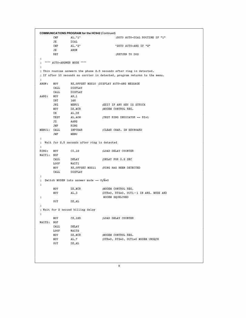
; **** AUTO-ANSWER MODE ****;
; This routine answers the phone 2.5 seconds after ring is detected.
; If after 10 seconds no carrier is detected, program returns to the menu.
;
ANSW: MOV BX,OFFSET MSG10 ;DISPLAY AUTO-ANS MESSAGE
CALL DISPLAY
CALL DISPLAY
AANS: MOV AH,1
INT 16H
JNZ MENU1 ;EXIT IF ANY KEY IS STRUCK
MOV DX,MCR ;MODEM CONTROL REG.
IN AL,DX
TEST AL,40H ;TEST RING INDICATOR Ð RI41
JZ AANS
JMP RING
MENU1: CALL INPCHAR ;CLEAR CHAR. IN KEYBOARD
JMP MENU
;
; Wait for 2.5 seconds after ring is detected
;
RING: MOV CI,12 ;LOAD DELAY COUNTER
WAIT1: NOP
CALL DELAY ;DELAY FOR 0.2 SEC
LOOP WAIT1
MOV BX,OFFSET MSG11 ;RING HAS BEEN DETECTED
CALL DISPLAY
;
; Switch MODEN into answer mode Ð O/A40
;
MOV DX,MCR ;MODEM CONTROL REG.
MOV AL,3 ;DTR40, RTS40, OUT1e1 IN ANS. MODE AND
; MODEM SQUELCHED
OUT DX,AL
;
; Wait for 2 second billing delay
;
MOV CX,12D ;LOAD DELAY COUNTER
WAIT2: NOP
CALL DELAY
LOOP WAIT2
MOV DX,MCR ;MODEM CONTROL REG.
MOV AL,7 ;DTR40, RTS40, OUT140 MODEM UNSQCH
OUT DX,AL
9

COMMUNICATIONS PROGRAM for the HC942 (Continued)
;
; Poll for carrier. Timeout after 10 seconds
;
MOV CX,500 ;LOAD TIMEOUT COUNTER
CARR: MOV DX,MSR
IN AL,DX
TEST AL,80H ;TEST FOR CARRIER Ð DCD41
JMZ COMM1
CALL DELAY ;WAIT 0.2 SEC THEN POLL AGAIN
LOOP CARR
JMP NC
COMM1: JMP COMM ;GO TO MAIN PROGRAM
;
; No carrier detected after answering phone, hang up and go back
; to auto-answer routine
;
NC: MOV BX,OFFSET MSG12
CALL DISPLAY
MOV DX,MCR ;MODEM CONTROL REG.
MOV AL,00 ;CODE TO HANG UP PHONE
OUT DX,AL
JMP ANSW
;
; **** DIALING ROUTINE ****;
; Determine long distance or local call
;
DIAL; MOV BX,OFFSET MSG1 ;DISPLAY OPENING MESS.
CALL DISPLAY
IMP: MOV BX,OFFSET MSG2 ;‘ LONG DISTANCE? ‘
CALL DISPLAY
CALL INPCHAR ;INPUT CHAR.
CALL DISPCHAR ;DISPLAY CHAR.
CALL CRÐLF ;kCRl AND kLFl
CMP AL,’N’ ;IS CHAR. A ‘n‘ OR A ‘N‘
JE SHT
CMP AL,’n’
JE SHT
;
; Enter long distance phone number into buffer
;
MOV BX,OFFSET MSG3 ;PROMPT FOR LONG DIS. CALL
CALL DISPLAY
MOV BX,OFFSET BUFF ;STARTING OFFSET OF BUFFER
MOV CL,LDPH ;COUNTER LONG DIS. PH. NUMBER AND kCRl
CALL BUFFER ;ENTER PH. NO. INTO BUFFER
CALL CRÐLF ;kCRl AND kLFl
JMP 0FFHK
10

COMMUNICATIONS PROGRAM for the HC942 (Continued)
;
; Enter local phone number into buffer
;
SHT: MOV BX,OFFSET MSG4 ;PROMPT FOR LOCAL CALL
CALL DISPLAY
MOV BX,OFFSET BUFF ;STARTING OFFSET OF BUFFER
MOV CL,LOCPH ;COUNTER FOR LOCAL PH. NUMBER AND kCRl
CALL BUFFER
CALL CRÐLF ;kCRl AND kLFl
;
; Take phone off-hook Ð DTR40. OUT141, OUT240
;
0FFHK: MOV DX,MCR ;MODEM CONTROL REG.
MOV AL,05H ;DTR40, OUT141,
OUT DX,AL ; OUT240 MODEM IS POWERED DOWN
;
; Wait for 2 sec. to get a dial tone
;
MOV CX,100
LOOP2: NOP
CALL DELAY ;WAIT FOR 200 ms
LOOP LOOP2 ;LOOP BACK 10 TIMES FOR A TOTAL OF 2000 ms
;
; Dial phone number: Get number from buffer, send data to TP5088 for
; 80 ms and off 120 ms. This is continued until a
; kCRl is encountered.
;
CLI ;DISABLE INTR. OF 8088
MOV BX,OFFSET MSG6 ;DISPLAY MESSAGE6
CALL DISPLAY
CALL CRÐLF ;kCRl AND kLFl
MOV BX,OFFSET BUFF ;MOVE TO STARTING ADDR. OF BUFFER
LOOP3: MOV DX,TP5088 ;ADDR. TP5088
MOV AL,[BX] ;INPUT CHAR. FROM BUFFER
CMP AL,0DDH ;IS CHAR. A DD HEX
JE CD ;YES, END DIALING
OUT DX,AL
CALL DELAY ;WAIT 200 ms
INC BX
JMP LOOP3
;
; Wait for carrier detection or timeout
;
CD: STI ;ENABLE INTR. OF 8088
MOV DX,MCR ;MODEM CONTROL REG.
MOV AL,1 ;TAKE MODEM OUT OF POWER DOWN MODE
OUT DX,AL
CALL DELAY ;WAIT FOR 0.4 SEC
CALL DELAY
MOV CX,1000
11

COMMUNICATIONS PROGRAM for the HC942 (Continued)
LOOP4 MOV DX,MSR ;MODEM STATUS REG.
IN AL,DX
TEST AL,80H ;TEST FOR DCD40
JNZ COMM
CALL DELAY ;WAIT 200 ms, THEN CK, DCD AGAIN
LOOP LOOP4
;
No answer after 20 sec., hang up, then call again or return to DOS?
;
MOV DX,MCR ;MODEM CONTROL REG.
MOV AL,00 ;CODE TO UART TO HANG UP PHONE
OUT DX,AL
MOV BX,OFFSET MSG5 ;‘ NO ANS., CALL AGAIN? ‘
CALL DISPLAY
CALL INPCHAR ;INPUT CHAR.
CALL DISPCHAR ;ECHO CHAR.
CALL CRÐLF ;kCRl AND kLFl
CMP AL,’Y’ ;IS CHAR. A ‘Y‘ OR A ‘y‘
JE BACK
CMP AL,’y’
JE BACK
JMP MENU ;GO BACK TO MAIN MENU
BACK: JMP 0FFHK
; **** MAIN PROGRAM ****; This is the communication routine. The Line Status
; Register is constantly polled for incoming and outgoing
; characters.
;
COMM: MOV DX,MCR ;MODEM CONTROL REGISTER
MOV AL,05H ;DTR40, OUT140 Ð MODEM IS UNSQUELCHED
OUT DX,AL
MOV BX,OFFSET MSG9 ;INDICATE THAT CARRIER IS DETECTED
CALL DISPLAY
CALL CRÐLF ;kCRl AND kLFl
MAIN: MOV DX,LSR ;LINE CONTROL REG.
IN AL,DX ;INPUT LINE STATUS FROM UART
TEST AL,1EH ;ERROR CONDITION?
JNZ ERROR
TEST AL,01H ;DATA RECEIVED?
JNZ REC
TEST AL,20H ;TRANSMISSION READY?
JZ MAIN
MOV DX,MSG ;MODEM STATUS REG.
IN AL,DX
TEST AL,80H ;DCD41? OR DATA CARRIER LOST?
JZ RTRN
;
; Check keyboard for key strike
;
MOV AH,1
INT 16H
JZ MAIN ;POLL AGAIN IF NO KEY STRIKE
12

COMMUNICATIONS PROGRAM for the HC942 (Continued)
;
; Input character from keyboard and send it to the UART
;
MOV AH,0
INT 16H
MOV DX,THR ;TRANSMISSION HOLDING REG.
OUT DX,AL ;SEND CHAR. TO UART
JMP MAIN
;
; **** Data received routine: read data from UART and display it
;
; Read data from the UART
;
REC: MOV DX,RBR ;REC. BUFFER REG.
IN AL,DX
AND AL,7FH ;STRIP OFF MSB
PUSH AX ;SAVE AX
;
; Display character obtain from UART
;
MOV BX,0
MOV AH,14
INT 10H ;DISPLAY CHAR. ON CRT
POP AX ;RESTORE AX
CMP AL,0DH ;IS CHAR A kCRl?
JE CR
CMP AL,03H ;IS CHAR. A >C?
JE RTRN
JMP MAIN
;
; If kCRl is hit, then add a kLFl
;
CR: MOV AL,0AH ;kLFl
MOV BX,0
MOV AH,14
INT 10H
JMP MAIN
;
; If >C is hit, then hang up and return to main menu
;
RTRN: MOV BX,OFFSET MSG8
CALL DISPLAY
MOV DX,MCR ;MODEM CONTROL REG.
MOV AL,00 ;SEND CODE TO UART HANG UP PH. LINE
OUT BX,AL
JMP MENU ;RETURN TO MAIN MENU
;
; **** Error routine: display a ‘?‘ if there is a transmission error
;
ERROR: MOV DX,RBR ;RECEIVER BUFFER REG.
IN AL,BX ;CLEAR REC. BUFFER OF ERRONEOUS DATA
MOV AL,’?’
MOV BX,0
13

COMMUNICATIONS PROGRAM for the HC942 (Continued)
MOV AH,14
INT 10H ;DISPLAY A ‘?’ ON CRT
JMP MAIN
;****************************************************************************************;
;
; ‘BUFFER‘ subroutine - places phone number in buffer (BUFF)
; Entry: BX4offset of buffer
; CL4counter of phone number digits
; Output: BX,CL altered
;
;****************************************************************************************PUBLIC BUFFER
BUFFER PROC NEAR
MOV CH,CL ;SAVE DIGIT COUNTER
INPT: CALL INPCHAR ;INPUT CHAR.
CALL DISPCHAR ;ECHO CHAR.
CMP AL,’1’ ; IS CHAR. A ’1’
JE INPT
CMP AL,’0’ ;IS CHAR. A ‘0‘
JE ZERO
PUSH AX ;SAVE AX
SUB AL,30H ;CONVERT ASCII TO BINARY
MOV [BX],AL ;MOVE DIGIT INTO BUFFER
CONT: INC BX
DEC CL
POP AX
CMP AL,00H ;IS CHAR. A kCRl?
JE CX
JMP INPT
CK: CMP CL,0 ;IS COUNTER40
JE EXIT1
MOV BX,OFFSET ERR ;DISPLAY ERROR MESSAGE IF BAD ENTRY
CALL DISPLAY
MOV BX,OFFSET BUFF ;RE-ENTER STARTING OFFSET OF BUFFER
MOV CL,CH ;RE-ENTER DIGIT COUNTER
JMP INPT
ZERO: PUSH AX ;SAVE AL
MOV AL,0AH ;CODE TO DIAL A ZERO
MOV [BX],AL ;MOVE ‘ZERO‘ DIGIT INTO BUFFER
JMP CONT
EXIT1: RET ;RETURN TO PHONE DIAL ROUTINE
BUFFER ENDP
;****************************************************************************************;
; ‘DELAY‘ subroutine - waits for 200 ms
; Entry: none
; Output: all register preserved
;
;****************************************************************************************PUBLIC DELAY
14

COMMUNICATIONS PROGRAM for the HC942 (Continued)
DELAY PROC NEAR
PUSH CX
MOV CX,34000D ;LOOP BACK 34,000 TIMES
LOOP5: NOP
ADD AL,1
SUB AL,1
LOOP LOOP5
POP CX
RET ;RETURN TO PHONE DIAL ROUTINE
DELAY ENDP
;****************************************************************************************;
; ‘INPCHAR‘ subroutine - invokes BIOS routine to input char. from keybd.
; Entry: none
; Output: AL4character entered from keyboard
;****************************************************************************************PUBLIC INPCHAR
INPCHAR PROC NEAR
MOV AH,0
INT 16H
RET
INPCHAR ENDP
;****************************************************************************************;
; ‘DISPLAY‘ subroutine - display a character string stored in the data
; segment.
; Entry: BX4offset of message string
; Output: BX altered
;
;****************************************************************************************PUBLIC DISPLAY
DISPLAY PROC NEAR
PUSH CX
PUSH AX
MOV CX,40D ;CHAR. STRING IS 40 CHAR. LONG
DISP1: MOV AL,[BX] ;SET CHAR. FROM DATA SEG.
CALL DISPCHAR ;DISPLAY CHAR.
INC BX
LOOP DISP1
CALL CRÐLF
POP AX
POP CX
RET ;RETURN TO PHONE DIAL ROUTINE
DISPLAY ENDP
;****************************************************************************************;
; ‘DISPCHAR‘ subroutine - invokes BIOS routine to display a character
in AL on the screen
; Entry: AL4character to be displayed
; Output: AX altered
;
;****************************************************************************************PUBLIC DISPCHAR
15

AN
-444
Sin
gle
-Chip
Modem
Pro
vid
es
Low
-CostD
ata
Com
munic
ation
COMMUNICATIONS PROGRAM for the HC942 (Continued)
DISPCHAR PROC NEAR
PUSH BX
MOV BX,0
MOV AH,14
INT 10H
POP BX
RET ;RETURN TO PHONE DIALING ROUTINE
DISPCHAR ENDP
;****************************************************************************************;
; ‘CRÐLF‘ subroutine - produces a carriage return and line feed
; Entry: none
; Output: all register preserved
;
;****************************************************************************************PUBLIC CRÐLF
CRÐLF PROC NEAR
PUSH AX
MOV AL,0DH ;CARRIAGE RETURN
CALL DISPCHAR
MOV AL,0AH ;LINE FEED
CALL DISPCHAR
POP AX
RET ;RETURN TO PHONE DIALING ROUTINE
CRÐLF ENDP
;
;
START1 ENDP
CODE ENDS
END START1
LIT. Ý 100444
LIFE SUPPORT POLICY
NATIONAL’S PRODUCTS ARE NOT AUTHORIZED FOR USE AS CRITICAL COMPONENTS IN LIFE SUPPORT
DEVICES OR SYSTEMS WITHOUT THE EXPRESS WRITTEN APPROVAL OF THE PRESIDENT OF NATIONAL
SEMICONDUCTOR CORPORATION. As used herein:
1. Life support devices or systems are devices or 2. A critical component is any component of a life
systems which, (a) are intended for surgical implant support device or system whose failure to perform can
into the body, or (b) support or sustain life, and whose be reasonably expected to cause the failure of the life
failure to perform, when properly used in accordance support device or system, or to affect its safety or
with instructions for use provided in the labeling, can effectiveness.
be reasonably expected to result in a significant injury
to the user.
National Semiconductor National Semiconductor National Semiconductor National SemiconductorCorporation Europe Hong Kong Ltd. Japan Ltd.1111 West Bardin Road Fax: (a49) 0-180-530 85 86 13th Floor, Straight Block, Tel: 81-043-299-2309Arlington, TX 76017 Email: cnjwge@ tevm2.nsc.com Ocean Centre, 5 Canton Rd. Fax: 81-043-299-2408Tel: 1(800) 272-9959 Deutsch Tel: (a49) 0-180-530 85 85 Tsimshatsui, KowloonFax: 1(800) 737-7018 English Tel: (a49) 0-180-532 78 32 Hong Kong
Fran3ais Tel: (a49) 0-180-532 93 58 Tel: (852) 2737-1600Italiano Tel: (a49) 0-180-534 16 80 Fax: (852) 2736-9960
National does not assume any responsibility for use of any circuitry described, no circuit patent licenses are implied and National reserves the right at any time without notice to change said circuitry and specifications.