Embed Size (px)
Citation preview

User's GuideSNOA873B–June 2012–Revised May 2013
AN-2264 LMH2121 Evaluation Board
1 General Description
The LMH2121 is an accurate fast responding power detector/RF envelope detector. Its response betweenan RF input signal and DC output signal is linear. The typical response time of 165 ns making it suitablefor an accurate power setting in handsets during a rise-time of RF transmission slots. It can be used in allpopular communication standards 2G/3G/4G/WAP.
The LMH2121 has an input range from –28 dBm to +12 dBm. Over this input range the device has anintrinsic high insensitivity on temperature, supply voltage and loading. The bandwidth of the device is from100 MHz to 3 GHz, covering 2G/3G/4G/WiFi wireless bands.
As a result of the unique internal architecture, the device shows an extremely low part-to-part variation ofthe detection curve. This is demonstrated by its low intercept and slope variation as well as a very goodlinear conformance. Consequently the required characterization and calibration efforts are low.
The device is active for EN = High, otherwise it is in a low power consumption shutdown mode. To savepower and enable the possibility for 2 detector outputs in parallel, the output (OUT) is high impedanceduring shutdown.
The LMH2121 is offered in a tiny 4-bump DSBGA package: 0.866mm x 1.07 mm x 0.6 mm.
All trademarks are the property of their respective owners.
1SNOA873B–June 2012–Revised May 2013 AN-2264 LMH2121 Evaluation BoardSubmit Documentation Feedback
Copyright © 2012–2013, Texas Instruments Incorporated

Basic Operation www.ti.com
Figure 1 shows the LMH2121 Evaluation Board.
Figure 1. LMH2121 Evaluation Board
2 Basic Operation
The circuit operates with a single supply form 2.6V to 3.3V and has an RF power detection range from−28 dBm to +12 dBm. The board consist of a single LMH2121 along with external components solderedon a printed circuit board (PCB_. External supply voltages and input signals can be applied to the on-board connectors. The supply voltage is applied with connectors P2 (VDD) and P3 (GND). The RF inputsignal is applied by SMA connector P1. This RF signal is applied through an RF generator and isconnected with a 50Ω SMA cable. The detector output can be measured via BNC connector P4.
3 Configuration
The LMH2121 evaluation board can be configured via jumper settings. The device is active when EN =High. This can be accomplished by setting the jumper J1 to VDD or by using external control on P5 bysetting the jumper J1 to EN.
2 AN-2264 LMH2121 Evaluation Board SNOA873B–June 2012–Revised May 2013Submit Documentation Feedback
Copyright © 2012–2013, Texas Instruments Incorporated

www.ti.com Configuration
An overview of the various jumper positions on the board is given in Figure 2. The settings of the jumperand its function is listed in Table 1.
Figure 2. Jumper Positions
Table 1. Jumper and Header Overview (1)
JumperJumper Function Position Description
J1 Enable 1–2 Active, Connects Enable Pin to VDD
3–4 External Control, Connects Enable Pin to Enable P5
5-6 Shutdown, Connects Enable Pin to GND(1) Jumper settings refer to the factory default configuration.
3SNOA873B–June 2012–Revised May 2013 AN-2264 LMH2121 Evaluation BoardSubmit Documentation Feedback
Copyright © 2012–2013, Texas Instruments Incorporated

-40 -30 -20 -10 0 10 20
10
1
0.1
0.01
2.6 GHz
RF INPUT POWER (dBm)
VO
UT (
V)
1.7 GHz
1.9 GHz100 MHz
700 MHz
900 MHz
FREQUENCY (Hz)
VO
UT (
V)
10
1
0.1
0.0110M 100M 1G 10G
RFIN = -25 dBm
RFIN = -10 dBm
RFIN = -5 dBm
RFIN = 0 dBm
RFIN = -15 dBm
RFIN = -20 dBm
RFIN = -30 dBm
RFIN = 5 dBm
RFIN = 10 dBm
RFIN
OUT
LMH2121Eval
Board
VDD
GND
GND
VDD
PowerSupply
RF SignalGenerator
DigitalVolt
Meter
Measurement Setup www.ti.com
4 Measurement Setup
The performance of the LMH2121 can be measured with the setup shown in Figure 3.
Figure 3. Measurement Setup
An external power supply provides a voltage of 2.7V to 3.3V to the evaluation board. An accurate andstable RF signal generator is used to produce the test signal. Use of low loss cables is recommended toensure reliable measurement data. The detected output voltage can be measured with a digital voltagemeter (DVM).
Figure 5-a depicts the output voltage versus frequency for various power levels on RFIN. The frequencyrange is from 10 MHz to 10 GHz. Figure 5-b depicts the output voltage versus RF input power for variousfrequencies.
Figure 4. (a) Output Voltage vs. Freqency Figure 5. (b) Output Voltage vs. RF Input Power
Figure 6. Output Voltage vs. Freqency and Output Voltage vs. RF Input Power
4 AN-2264 LMH2121 Evaluation Board SNOA873B–June 2012–Revised May 2013Submit Documentation Feedback
Copyright © 2012–2013, Texas Instruments Incorporated

www.ti.com Schematic
5 Schematic
Figure 7. Evaluation Board Schematic
5SNOA873B–June 2012–Revised May 2013 AN-2264 LMH2121 Evaluation BoardSubmit Documentation Feedback
Copyright © 2012–2013, Texas Instruments Incorporated
Bill of Material www.ti.com
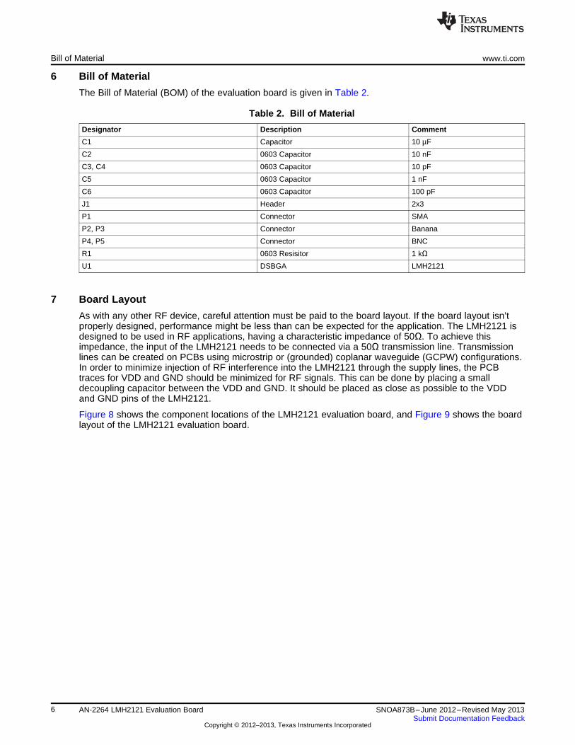
6 Bill of Material
The Bill of Material (BOM) of the evaluation board is given in Table 2.
Table 2. Bill of Material
Designator Description Comment
C1 Capacitor 10 µF
C2 0603 Capacitor 10 nF
C3, C4 0603 Capacitor 10 pF
C5 0603 Capacitor 1 nF
C6 0603 Capacitor 100 pF
J1 Header 2x3
P1 Connector SMA
P2, P3 Connector Banana
P4, P5 Connector BNC
R1 0603 Resisitor 1 kΩU1 DSBGA LMH2121
7 Board Layout
As with any other RF device, careful attention must be paid to the board layout. If the board layout isn’tproperly designed, performance might be less than can be expected for the application. The LMH2121 isdesigned to be used in RF applications, having a characteristic impedance of 50Ω. To achieve thisimpedance, the input of the LMH2121 needs to be connected via a 50Ω transmission line. Transmissionlines can be created on PCBs using microstrip or (grounded) coplanar waveguide (GCPW) configurations.In order to minimize injection of RF interference into the LMH2121 through the supply lines, the PCBtraces for VDD and GND should be minimized for RF signals. This can be done by placing a smalldecoupling capacitor between the VDD and GND. It should be placed as close as possible to the VDDand GND pins of the LMH2121.
Figure 8 shows the component locations of the LMH2121 evaluation board, and Figure 9 shows the boardlayout of the LMH2121 evaluation board.
6 AN-2264 LMH2121 Evaluation Board SNOA873B–June 2012–Revised May 2013Submit Documentation Feedback
Copyright © 2012–2013, Texas Instruments Incorporated

www.ti.com LMH2121 Evaluation Board
8 LMH2121 Evaluation Board
Figure 8. Component Locations of Evaluation Board Figure 9. Board Layout of Evaluation Board
7SNOA873B–June 2012–Revised May 2013 AN-2264 LMH2121 Evaluation BoardSubmit Documentation Feedback
Copyright © 2012–2013, Texas Instruments Incorporated

IMPORTANT NOTICE
Texas Instruments Incorporated and its subsidiaries (TI) reserve the right to make corrections, enhancements, improvements and otherchanges to its semiconductor products and services per JESD46, latest issue, and to discontinue any product or service per JESD48, latestissue. Buyers should obtain the latest relevant information before placing orders and should verify that such information is current andcomplete. All semiconductor products (also referred to herein as “components”) are sold subject to TI’s terms and conditions of salesupplied at the time of order acknowledgment.
TI warrants performance of its components to the specifications applicable at the time of sale, in accordance with the warranty in TI’s termsand conditions of sale of semiconductor products. Testing and other quality control techniques are used to the extent TI deems necessaryto support this warranty. Except where mandated by applicable law, testing of all parameters of each component is not necessarilyperformed.
TI assumes no liability for applications assistance or the design of Buyers’ products. Buyers are responsible for their products andapplications using TI components. To minimize the risks associated with Buyers’ products and applications, Buyers should provideadequate design and operating safeguards.
TI does not warrant or represent that any license, either express or implied, is granted under any patent right, copyright, mask work right, orother intellectual property right relating to any combination, machine, or process in which TI components or services are used. Informationpublished by TI regarding third-party products or services does not constitute a license to use such products or services or a warranty orendorsement thereof. Use of such information may require a license from a third party under the patents or other intellectual property of thethird party, or a license from TI under the patents or other intellectual property of TI.
Reproduction of significant portions of TI information in TI data books or data sheets is permissible only if reproduction is without alterationand is accompanied by all associated warranties, conditions, limitations, and notices. TI is not responsible or liable for such altereddocumentation. Information of third parties may be subject to additional restrictions.
Resale of TI components or services with statements different from or beyond the parameters stated by TI for that component or servicevoids all express and any implied warranties for the associated TI component or service and is an unfair and deceptive business practice.TI is not responsible or liable for any such statements.
Buyer acknowledges and agrees that it is solely responsible for compliance with all legal, regulatory and safety-related requirementsconcerning its products, and any use of TI components in its applications, notwithstanding any applications-related information or supportthat may be provided by TI. Buyer represents and agrees that it has all the necessary expertise to create and implement safeguards whichanticipate dangerous consequences of failures, monitor failures and their consequences, lessen the likelihood of failures that might causeharm and take appropriate remedial actions. Buyer will fully indemnify TI and its representatives against any damages arising out of the useof any TI components in safety-critical applications.
In some cases, TI components may be promoted specifically to facilitate safety-related applications. With such components, TI’s goal is tohelp enable customers to design and create their own end-product solutions that meet applicable functional safety standards andrequirements. Nonetheless, such components are subject to these terms.
No TI components are authorized for use in FDA Class III (or similar life-critical medical equipment) unless authorized officers of the partieshave executed a special agreement specifically governing such use.
Only those TI components which TI has specifically designated as military grade or “enhanced plastic” are designed and intended for use inmilitary/aerospace applications or environments. Buyer acknowledges and agrees that any military or aerospace use of TI componentswhich have not been so designated is solely at the Buyer's risk, and that Buyer is solely responsible for compliance with all legal andregulatory requirements in connection with such use.
TI has specifically designated certain components as meeting ISO/TS16949 requirements, mainly for automotive use. In any case of use ofnon-designated products, TI will not be responsible for any failure to meet ISO/TS16949.
Products Applications
Audio www.ti.com/audio Automotive and Transportation www.ti.com/automotive
Amplifiers amplifier.ti.com Communications and Telecom www.ti.com/communications
Data Converters dataconverter.ti.com Computers and Peripherals www.ti.com/computers
DLP® Products www.dlp.com Consumer Electronics www.ti.com/consumer-apps
DSP dsp.ti.com Energy and Lighting www.ti.com/energy
Clocks and Timers www.ti.com/clocks Industrial www.ti.com/industrial
Interface interface.ti.com Medical www.ti.com/medical
Logic logic.ti.com Security www.ti.com/security
Power Mgmt power.ti.com Space, Avionics and Defense www.ti.com/space-avionics-defense
Microcontrollers microcontroller.ti.com Video and Imaging www.ti.com/video
RFID www.ti-rfid.com
OMAP Applications Processors www.ti.com/omap TI E2E Community e2e.ti.com
Wireless Connectivity www.ti.com/wirelessconnectivity
Mailing Address: Texas Instruments, Post Office Box 655303, Dallas, Texas 75265Copyright © 2013, Texas Instruments Incorporated