Embed Size (px)
Citation preview

User's GuideSNVA446B–June 2010–Revised February 2014
AN-2067 LM5027A Evaluation Board
1 IntroductionThe LM5027A evaluation board is designed to provide the design engineer with a fully functional powerconverter based on the Active Clamp Forward topology to evaluate the LM5027A controller. Theevaluation board is provided in an industry standard quarter-brick footprint.
The performance of the evaluation board is:• Input Operating Range: 36 to 78 V (100 V peak)• Output Voltage: 3.3 V• Output Current: 0 to 30 A• Measured Efficiency: 90.5% @ 30 A, 92.5% @ 15 A• Frequency of Operation: 250 kHz• Board Size: 2.3 × 1.45 × 0.5 inches• Load Regulation: 1%• Line Regulation: 0.1%• Line UVLO, Hiccup Current Limit• A 70% Maximum Duty Cycle
The printed circuit board consists of 6 layers of 2 ounce copper on FR4 material with a total thickness of0.050 inches. The unit is designed for continuous operation at rated load at <40°C and a minimum airflowof 200 CFM.
2 Theory of OperationPower converters based on the Forward topology offer high efficiency and good power handling capabilityin applications up to several hundred watts. The operation of the transformer in a forward topology doesnot inherently self-reset each power switching cycle; a mechanism to reset the transformer is required.The active clamp reset mechanism is presently finding extensive use in medium level power converters inthe 50 to 200 W range.
The Forward converter is derived from the Buck topology family, employing a single modulating powerswitch. The main difference between the topologies are, the Forward topology employs a transformer toprovide input / output ground isolation and a step down or step up function.
Each cycle, the main primary switch turns on and applies the input voltage across the primary winding,which has 12 turns. The transformer secondary has 2 turns, leading to a 6:1 step-down of the inputvoltage. For an output voltage of 3.3 V the required duty cycle (D) of the main switch must vary fromapproximately 60% (low line) to 25% (high line). The LM5027A limits the PWM duty cycle output to amaximum of 70% (typical). The maximum duty cycle limits the voltage stress on the Active Clamp Forwardconverter MOSFETs. The clamp capacitor along with the reset switch reverse biases the transformerprimary each cycle when the main switch turns off. This reverse voltage resets the transformer. The clampcapacitor voltage is Vin / (1-D).
All trademarks are the property of their respective owners.
1SNVA446B–June 2010–Revised February 2014 AN-2067 LM5027A Evaluation BoardSubmit Documentation Feedback
Copyright © 2010–2014, Texas Instruments Incorporated

CS
VIN
UVLO
OTP
RAMP
TIME3
REF
RT
TIME1
TIME2
SS
RES
SSSR
COMP
OUTA
OUTB
OUTSR
AGND PGND
VCC
ERROR AMP and ISOLATION
VOUTVIN
LM5027A
Evaluation Board Schematic www.ti.com
Feedback from the output is processed by an amplifier and reference, generating an error voltage, whichis coupled back to the primary side control through an optocoupler. The LM5027A voltage mode controllerpulse width modulates the error signal with a ramp signal derived from the input voltage. Deriving theramp signal slope from the input voltage provides line feed-forward, which improves line transientrejection. The LM5027A also provides a controlled delay necessary for the reset switch. The evaluationboard can be synchronized to an external clock with a recommended frequency range of 275 to 300 kHz.
3 Evaluation Board Schematic
Figure 1. Evaluation Board Schematic
4 Powering and Loading ConsiderationsWhen applying power to the LM5027A evaluation board certain precautions need to be followed. A failureor misconnection can present itself in a very alarming manner.
4.1 Proper ConnectionsWhen operated at low input voltages the evaluation board can draw up to 3.5 A of current at full load. Themaximum rated output current is 30 A. Be sure to choose the correct connector and wire size whenattaching the source supply and the load. Monitor the current into and out of the evaluation board. Monitorthe voltage directly at the output terminals of the evaluation board. The voltage drop across the loadconnecting wires will give inaccurate measurements; this is especially true for accurate efficiencymeasurements. See Figure 2.
2 AN-2067 LM5027A Evaluation Board SNVA446B–June 2010–Revised February 2014Submit Documentation Feedback
Copyright © 2010–2014, Texas Instruments Incorporated

Scope Volt-meter Volt-meter Current-meter
80 Volt, 5 Amp Power Supply with Current
Meter
200 Watt, 60 Amp Electronic
Load-
+
+
-
+
Evaluation Board
ON/OFF(SHUTDOWN)
IN OUT
Jumper
www.ti.com Powering and Loading Considerations
Figure 2. Typical Evaluation Setup
4.2 Source PowerThe evaluation board can be viewed as a constant power load. At low input line voltage (36 V) the inputcurrent can reach 3.5 A, while at high input line voltage (78 V) the input current will be approximately 1.5A. Therefore too fully test the LM5027A evaluation board a DC power supply capable of at least 80 V and4 A is required. The power supply must have adjustments for both voltage and current. An accuratereadout of output current is desirable since the current is not subject to loss in the cables as voltage is.The power supply and cabling must present a low impedance to the evaluation board. Insufficient cablingor a high impedance power supply will droop during power supply application with the evaluation boardinrush current. If large enough, this droop will cause a chattering condition upon power up. This chatteringcondition is an interaction with the evaluation board undervoltage lockout, the cabling impedance and theinrush current.
4.3 LoadingAn appropriate electronic load, with specified operation down to 3.0 V minimum, is desirable. Theresistance of a maximum load is 0.11 Ω. You need thick cables! Consult a wire chart if needed. If resistorbanks are used there are certain precautions to be taken. The wattage and current ratings must beadequate for a 30 A, 100 W supply. Monitor both current and voltage at all times. Ensure there is sufficientcooling provided for the load.
4.4 Air FlowAn appropriate electronic load, with specified operation down to 3.0 V minimum, is desirable. Theresistance of a maximum load is 0.11 Ω. You need thick cables! Consult a wire chart if needed. If resistorbanks are used there are certain precautions to be taken. The wattage and current ratings must beadequate for a 30 A, 100 W supply. Monitor both current and voltage at all times. Ensure there is sufficientcooling provided for the load.
4.5 Powering UpUsing the shutdown pin provided will allow powering up the source supply with the current level set low. Itis suggested that the load be kept quite nominal during the first power up. Set the current limit of thesource supply to provide about 1.5 times the wattage of the load. As you remove the connection from theshutdown pin to ground, immediately check for 3.3 V at the output.
A most common occurrence, that will prove unnerving, is when the current limit set on the source supply isinsufficient for the load. The result is similar to having the high source impedance referred to earlier. Theinteraction of the source supply folding back and the evaluation board going into undervoltage shutdownwill start an oscillation, or chatter, that may have highly undesirable consequences.
3SNVA446B–June 2010–Revised February 2014 AN-2067 LM5027A Evaluation BoardSubmit Documentation Feedback
Copyright © 2010–2014, Texas Instruments Incorporated

Start-Up www.ti.com
A quick efficiency check is the best way to confirm that everything is operating properly. If something isamiss you can be reasonably sure that it will affect the efficiency adversely. Few parameters can beincorrect in a switching power supply without creating losses and potentially damaging heat.
4.6 Over Current ProtectionThe evaluation board is configured with hiccup over-current protection. In the event of an output overload(approximately 33 A) the unit will discharge the soft-start capacitor, which disables the power stage. Aftera delay the soft-start is released. The shutdown, delay and slow recharge time of the soft-start capacitorprotects the unit, especially during short circuit event where the stress is highest.
5 Start-UpPower supplies have a soft-start circuit(s) to control their output voltage when input power is applied. Thesoft-start sequence limits the peak inrush current as the output capacitors are charged, and prevents theoutput voltage from over-shooting. In most power supplies there are primary side and secondary side soft-start circuits.
The primary side soft-start circuit is generally in a primary side controller and the soft-start time is set withan external capacitor. The function of the primary side soft-start circuit is to slowly increasing the dutycycle of the controller from zero to the maximum duty cycle. The maximum duty cycle varies based on thecontroller and the circuit topology.
The secondary side soft-start circuit connects a resistor/capacitor from the secondary side voltagereference to the positive input of the error amplifier. The soft-start time is set by the resistor/capacitor timeconstant and works by ramping up the voltage reference on the secondary side error amplifier. The outputof the error amplifier is fed across the isolation boundary to the primary side controller compensation inputwhich is connected to the controller PWM input. The voltage at the compensation input increases to avalue required for regulation as determined by the voltage feedback loop. The secondary side soft-startalong with the primary side soft-start work together to control the duty cycle on start-up to controling thepower supplies output start-up time, and limit the stress on the power components.
Figure 3 shows the primary and secondary side soft-start sequence using the LM5027A into an electronicload. After Vin is applied the primary side soft-start ramps up. When the voltage on the LM5027A SS pinreached 1.0 V the output drives start and power is delivered to the secondary of the transformer. Thepower supply output rises and the secondary side soft-start circuit begins to ramp-up. The output of theDC-DC converter monotonically increased with no overshoot to 3.3 V out.
Figure 3. Soft-Start
4 AN-2067 LM5027A Evaluation Board SNVA446B–June 2010–Revised February 2014Submit Documentation Feedback
Copyright © 2010–2014, Texas Instruments Incorporated

LM5027A
UVLO
PGND AGND
COMP
OUT_A
OUT_B
VCC
SSRT SYNCREF
TIME
RAMP
CS1
VIN
VIN
35V - 78V
VOUT
3.3V
UP/DOWNSYNC
ERRORAMP and
ISOLATION
CS2
-+
www.ti.com Pre-Bias Load Start-Up
6 Pre-Bias Load Start-UpFigure 4 shows a typical Forward Converter topology with an active clamp using self-driven synchronousrectification. It’s simple and very efficient; however there are some disadvantages when starting thistopology into a pre-biased load. The first occurs because the synchronous rectification is on the secondaryside of the transformer and without adding intelligence the output current will flow into the converter via theoutput choke and the free wheeling MOSFET when the converter starts-up or shut down with pre-biasvoltage.
Figure 4. Typical Forward Converter
5SNVA446B–June 2010–Revised February 2014 AN-2067 LM5027A Evaluation BoardSubmit Documentation Feedback
Copyright © 2010–2014, Texas Instruments Incorporated

CS
VIN
UVLO
OTP
RAMP
TIME3
REF
RT
TIME1
TIME2
SS
RES
SSSR
COMP
OUTA
OUTB
OUTSR
AGND PGND
VCC
ERROR AMP and ISOLATION
VOUTVIN
LM5027A
OUTSR Drive www.ti.com
7 OUTSR DriveThe LM5027A has a dedicated pin (OUTSR) to drive the synchronous rectifier free wheeling MOSFETthrough a drive transformer as shown in Figure 5. When the converter starts-up, the OUTSR drive is heldlow and the freewheeling MOSFET is turned-off. As a result, no output current will sink into the converter.The OUTSR is enabled after the primary side soft-start reaches approximately 4.0 V. The OUTSR delaywas added to ensure that the power supply output voltage is up and in regulation prior to the freewheelingMOSFET being turned-on, refer to Figure 6 and Figure 7. The OUTSR drive is soft-started; a capacitor onthe SSSR pin is released and is charged with a 25 µA current source, slowly increasing the duty cycle ofthe freewheeling FET’s duty cycle.
Figure 5. LM5027A Synchronous Rectifier Drive Output (OUTSR)
6 AN-2067 LM5027A Evaluation Board SNVA446B–June 2010–Revised February 2014Submit Documentation Feedback
Copyright © 2010–2014, Texas Instruments Incorporated

SS
SSSR
OUTA, OUTBSoft-Start
OUTSRSoft-Start
OUTSRSoft-Stop
5V
5V
1V~3V
2.5V4.5V
UVLO
2V2.5V
4.5V
0.4V < UVLO < 2VUVLO > 2VUVLO < 2V
OUTB
SR
PWM
increasing OUTA SS pulse width
increasing SR SS pulse width
increasing PWM SS pulse width
OUTA
www.ti.com OUTSR Drive
Figure 6. LM5027A Drive Timing
Figure 7. LM5027A Soft-Start Waveforms
7SNVA446B–June 2010–Revised February 2014 AN-2067 LM5027A Evaluation BoardSubmit Documentation Feedback
Copyright © 2010–2014, Texas Instruments Incorporated

+SB
+VOUT
Feedback Optocoupler
Error Amplifier
+SB
+
-
CSS
Secondary Side Soft-Start www.ti.com
8 Secondary Side Soft-StartIn a typical DC-DC converter with a 3.3 V output the voltage reference for the error amplifier is 1.2 V. Priorto the power supply being turned-on and if there is a pre-bias load, the secondary side soft-start capacitor(CSS) will be pre-charged to the voltage reference level of 1.2 V (if the pre-bias load > 1.2 V), refer toFigure 8. On start-up the primary side soft-start begins and the output voltage rises from the pre-biasvoltage level to 3.3 V, refer to Figure 9. At the end of the primary side soft-start period the controller will beat maximum duty cycle and the output voltage will overshoot until the feedback error amplifier has achance to respond and reduce the output voltage to the regulation set point.
Figure 8. VREF with Pre-Bias Load
Figure 9. Pre-Bias Secondary Side Soft-Start
8 AN-2067 LM5027A Evaluation Board SNVA446B–June 2010–Revised February 2014Submit Documentation Feedback
Copyright © 2010–2014, Texas Instruments Incorporated

DOG
NOTES
Converter Ouput (Vout)
Secondary BiasSecondary Bias
Power Good
LM4041-1.2
Reference
47k
0.1 uF
47k
1000 pF
20k
Error
Amplifier
Opto-Coupler
Soft-Start
5k
47k
15k
24.9k
3.6V
1 uF
Frequency
Compensation
Feedback
Voltage
Q1
Q23.6V
To Forward/MOSFET enable
CBIAS
www.ti.com Secondary Side Soft-Start Reset
9 Secondary Side Soft-Start ResetWhen input power is supplied to the LM5027A Evaluation Board the LM5027A’s internal VCC Regulatorturns-on providing power to the VCC pin, the primary side soft-start voltage increases, and the outputdrives are enabled. When the drive outputs are enables the voltage on the transformer secondaryincreases, the Secondary Bias rises supplying voltage to the reference and error amplifier, refer toFigure 10. During this time FET Q1 is turned-on holding the reference voltage at the positive input to theerror amplifier low (zero volts). When the voltage on the secondary bias capacitor (CBIAS) rises above theZener diode> 3.6 V, the Secondary Bias Power Good (the collector of Q2) goes high. This turns-off FETQ1 allowing the secondary soft-start capacitor to charge up. This solution of reseting the soft-startcapacitor to zero (0 V) on start-up works for pre-bias loads as well as loads that do not need to start into apre-biased condition. This allows for a monotonic start-up under both operating modes.
Figure 10. Pre-Bias Schematic
9SNVA446B–June 2010–Revised February 2014 AN-2067 LM5027A Evaluation BoardSubmit Documentation Feedback
Copyright © 2010–2014, Texas Instruments Incorporated

OUTSR
Gate of the Sync MOSFET needs to be
isolated
T1
M1
R2
R1
Pre-Bias Load-Synchronous Forward MOSFET Enabled www.ti.com
10 Pre-Bias Load-Synchronous Forward MOSFET EnabledThe self driven synchronous rectification topology has an issues starting into a pre-bias load. When a pre-bias load is connected across the power supply output, refer to Figure 11, the pre-bias source will conductcurrent through the output inductor and the self driven gate drive resistors R1 and R2. If the pre-biasvoltage is greater than the Vgs of the synchronous MOSFET (M1), the MOSFET will be turned-on sinkingcurrent into the power supply.
Figure 11. Self Driven with Pre-Bias Load
10 AN-2067 LM5027A Evaluation Board SNVA446B–June 2010–Revised February 2014Submit Documentation Feedback
Copyright © 2010–2014, Texas Instruments Incorporated

nVin_max
VCE = 16.67 Vpk6
100==
www.ti.com Synchronous Forward MOSFET Enabled
11 Synchronous Forward MOSFET EnabledFor the LM5027A Evaluation board we used the Secondary Bias Power Good signal as a flag to indicatethat the primary sides MOSFETs are switching providing power to the secondary of the transformer T1.When the flag goes high this indicates that it is time to turn-on the forward conducting MOSFET M1. TheSecondary Bias Power Good signal drives the base of an NPN transistor (Q3), refer to Figure 13. TheNPN transistor is configured as a Cascod amplifier; when it is turned-on, the voltage on the secondary ofthe transformer T1 drives the gate of the synchronous MOSFET, M1. The MOSFET gate drive voltage is:
V-GATE_DRIVE_M1 = V_Secondary_Bias_Power_Good - VBE_Q3 (1)
An NPN transistor needs to be selected so that the transistors collector to emitter voltage under the worstcase operating condition does not exceed it’s VCE ratings, and that the collector current (Icc) can handlethe maximum peak current to drive the gate of MOSFET M1. For the LM5027A Evaluation board thetransistor is a 30 V, 1.5 ampere transistor. The maximum VCE is:
(2)
Where:
Vin = 100 V under transient conditions
n is the transformer turns ratio = 6
A diode D1 is connected from the collector to the emitter of Q3 to handle any voltage spikes as a result ofcircuit inductance. Without this diode inductive voltage spike may damage the Cascod amplifier Q3.
An NPN transistor was use instead of an N-Channel MOSFET because the Vgs drop, typically 4 to 5 V;this would reduce the gates drive voltage to M1. Under minimum input line conditions M1 may not be fullyturned-on and there would be an increase in the I2 × RDS(ON) losses.
Figure 12 shows the start-up waveforms for the Evaluation board. After the input power is supplied to theEvaluation board the secondary bias voltage rises, when the secondary bias is greater than 3.6 V, theSecondary Power Good output goes high. This turns-on M1 and enables the secondary side soft-startcircuit allowing the output voltage to increase after Vout > Vpre-bias.
An alternative to using the circuit in Figure 13 is shown in Figure 14; an additional winding can be addedto the power transformer which can be used to drive the Forward Synchronous Rectifier MOSFET (M1).This is a simple solution and should not add a lot of complexity to the transformer design.
Figure 12. Pre-Bias Load Waveforms
11SNVA446B–June 2010–Revised February 2014 AN-2067 LM5027A Evaluation BoardSubmit Documentation Feedback
Copyright © 2010–2014, Texas Instruments Incorporated

+
OUTSR
Gate of the Sync MOSFET needs to be
isolated
3.6V
Secondary Bias Power Good
Secondary Bias
CBIAS
Q1
Q3
M1
D1
Peak Rectifier
T1
Synchronous Forward MOSFET Enabled www.ti.com
Figure 13. Isolated Synchronous MOSFET
12 AN-2067 LM5027A Evaluation Board SNVA446B–June 2010–Revised February 2014Submit Documentation Feedback
Copyright © 2010–2014, Texas Instruments Incorporated

OUTSR
Gate of the Sync MOSFET is Drven by a winging on T1 and is
isolated
T1
www.ti.com Synchronous Forward MOSFET Enabled
Figure 14. Isolated Synchronous MOSFET Drive Using a Transformer
13SNVA446B–June 2010–Revised February 2014 AN-2067 LM5027A Evaluation BoardSubmit Documentation Feedback
Copyright © 2010–2014, Texas Instruments Incorporated

80 Volt, 5 AmpPower Supply
with Current Meter
Current probe
--
+
IN
Vout
LM5027 Evaluation Board
+
+
S+
S-
VoutRTN
1:
OSC scope220uF
Vout - 0.6 V
Pre-Bias Load Test Set-Up www.ti.com
12 Pre-Bias Load Test Set-UpFor the Pre-bias start-up test, the circuit in Figure 15 was used. An external bias supply, through a 1.0 Ωresistor, was connected across the output terminals of the Evaluation Board.
Figure 15. Pre-Bias Load Test Set-Up
13 Pre-Bias Load Start-Up RequirementsThe Evaluation board Pre-Bias start-up requirement is that during converter start-up the output shall risemonotonically and not sink current (into the converter) of more than 50 mA .
14 Evaluation Board ResultsFigure 16 shows the output of the Evaluation Board starting with a pre-bias voltage of 2.7 V. Under theseconditions the output voltage starts at 2.7 V and then increases monotonically to 3.3 V. The current intothe Evaluation board (sinking) is less than 50 mA. When the output voltage rise above the pre-bias voltagethere is approximately 400 mA of current out of (sourced) the Evaluation Board to charge the external 220µF capacitor. After the external capacitor is charge to 3.3 V the current out of the power supply drop toapproximately 50 mA.
Figure 16. Pre-Bias StartUp
14 AN-2067 LM5027A Evaluation Board SNVA446B–June 2010–Revised February 2014Submit Documentation Feedback
Copyright © 2010–2014, Texas Instruments Incorporated

www.ti.com Performance Characteristics
15 Performance Characteristics
15.1 Turn-On WaveformsWhen applying power to the LM5027A evaluation board a certain sequence of events occurs. Soft-startcapacitor values and other components allow for a minimal output voltage for a short time until thefeedback loop can stabilize without overshoot. Figure 17 shows the output voltage during a typical start-upwith a 48 V input and a load of 5 A. There is no overshoot during startup.
(1) Conditions:Input Voltage = 48 VDCOutput Current = 5 ATrace 1: Volts/div = 1.0 VOutput VoltageHorizontal Resolution = 1 ms/div
Figure 17. Turn-On Waveforms
15SNVA446B–June 2010–Revised February 2014 AN-2067 LM5027A Evaluation BoardSubmit Documentation Feedback
Copyright © 2010–2014, Texas Instruments Incorporated
Performance Characteristics www.ti.com
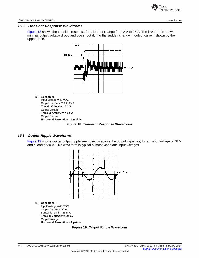
15.2 Transient Response WaveformsFigure 18 shows the transient response for a load of change from 2 A to 25 A. The lower trace showsminimal output voltage droop and overshoot during the sudden change in output current shown by theupper trace.
(1) Conditions:Input Voltage = 48 VDCOutput Current = 2 A to 25 ATrace1: Volts/div = 0.2 VOutput VoltageTrace 2: Amps/Div = 5.0 AOutput CurrentHorizontal Resolution = 1 ms/div
Figure 18. Transient Response Waveforms
15.3 Output Ripple WaveformsFigure 19 shows typical output ripple seen directly across the output capacitor, for an input voltage of 48 Vand a load of 30 A. This waveform is typical of most loads and input voltages.
(1) Conditions:Input Voltage = 48 VDCOutput Current = 30 ABandwidth Limit = 25 MHzTrace 1: Volts/div = 50 mVOutput VoltageHorizontal Resolution = 2 µs/div
Figure 19. Output Ripple Waveform
16 AN-2067 LM5027A Evaluation Board SNVA446B–June 2010–Revised February 2014Submit Documentation Feedback
Copyright © 2010–2014, Texas Instruments Incorporated

www.ti.com Performance Characteristics
15.4 Drain Voltage of Q1 with a 25 A LoadFigure 20 and Figure 21 show the drain voltage of Q1 with a 25 A load. Figure 20 represents an inputvoltage of 38 V and Figure 21 represents an input voltage of 78 V.
(1) Conditions:Input Voltage = 38 VDCOutput Current = 25 ATrace 1: Volts/Div = 20 VQ1 Drain VoltageHorizontal Resolution = 1 µs/div
Figure 20. Drain Voltage of Q1 with a 25 A Load - Input Voltage of 38 V
(1) Conditions:Input Voltage = 78 VDCTrace 1: Volts/Div = 20 VQ1 Drain VoltageHorizontal Resolution = 1 µs/div
Figure 21. Drain Voltage of Q1 with a 25 A Load - Input Voltage of 78 V
17SNVA446B–June 2010–Revised February 2014 AN-2067 LM5027A Evaluation BoardSubmit Documentation Feedback
Copyright © 2010–2014, Texas Instruments Incorporated

Performance Characteristics www.ti.com
15.5 Gate VoltagesFigure 22 shows the gate voltages of the synchronous rectifiers. The drive from the main powertransformer is delayed slightly at turn-on by a resistor interacting with the gate capacitance. This providesimproved switching transitions for optimum efficiency. The difference in drive voltage is inherent in thetopology and varies with line voltage
(1) Conditions:Input Voltage = 48 VDCOutput Current = 5 ATrace 3: (gate) Volts/Div = 2 VSynchronous Rectifier, Q3/Q4Trace 2: (gate) Volts/Div = 2 VSynchronous Rectifier, Q5/Q6Horizontal Resolution = 1 µs/div
Figure 22. Gate Voltages
15.6 Efficiency
Figure 23. Efficiency
18 AN-2067 LM5027A Evaluation Board SNVA446B–June 2010–Revised February 2014Submit Documentation Feedback
Copyright © 2010–2014, Texas Instruments Incorporated
www.ti.com Performance Characteristics
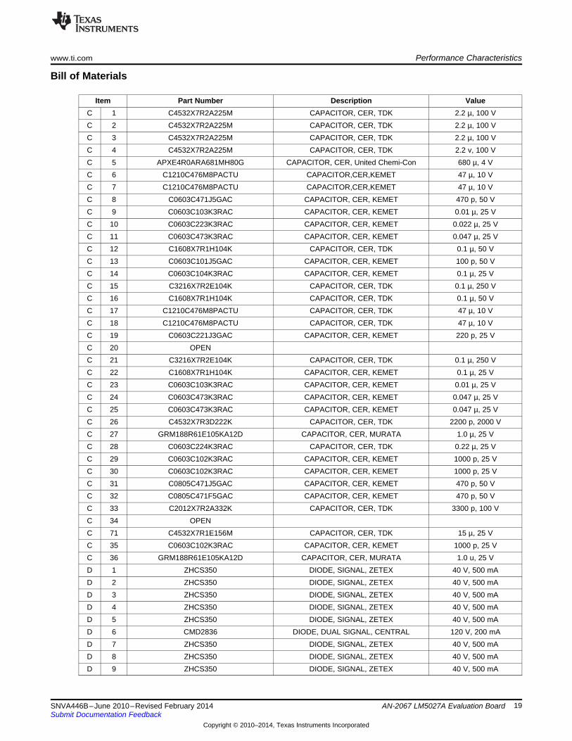
Bill of Materials
Item Part Number Description ValueC 1 C4532X7R2A225M CAPACITOR, CER, TDK 2.2 µ, 100 VC 2 C4532X7R2A225M CAPACITOR, CER, TDK 2.2 µ, 100 VC 3 C4532X7R2A225M CAPACITOR, CER, TDK 2.2 µ, 100 VC 4 C4532X7R2A225M CAPACITOR, CER, TDK 2.2 v, 100 VC 5 APXE4R0ARA681MH80G CAPACITOR, CER, United Chemi-Con 680 µ, 4 VC 6 C1210C476M8PACTU CAPACITOR,CER,KEMET 47 µ, 10 VC 7 C1210C476M8PACTU CAPACITOR,CER,KEMET 47 µ, 10 VC 8 C0603C471J5GAC CAPACITOR, CER, KEMET 470 p, 50 VC 9 C0603C103K3RAC CAPACITOR, CER, KEMET 0.01 µ, 25 VC 10 C0603C223K3RAC CAPACITOR, CER, KEMET 0.022 µ, 25 VC 11 C0603C473K3RAC CAPACITOR, CER, KEMET 0.047 µ, 25 VC 12 C1608X7R1H104K CAPACITOR, CER, TDK 0.1 µ, 50 VC 13 C0603C101J5GAC CAPACITOR, CER, KEMET 100 p, 50 VC 14 C0603C104K3RAC CAPACITOR, CER, KEMET 0.1 µ, 25 VC 15 C3216X7R2E104K CAPACITOR, CER, TDK 0.1 µ, 250 VC 16 C1608X7R1H104K CAPACITOR, CER, TDK 0.1 µ, 50 VC 17 C1210C476M8PACTU CAPACITOR, CER, TDK 47 µ, 10 VC 18 C1210C476M8PACTU CAPACITOR, CER, TDK 47 µ, 10 VC 19 C0603C221J3GAC CAPACITOR, CER, KEMET 220 p, 25 VC 20 OPENC 21 C3216X7R2E104K CAPACITOR, CER, TDK 0.1 µ, 250 VC 22 C1608X7R1H104K CAPACITOR, CER, KEMET 0.1 µ, 25 VC 23 C0603C103K3RAC CAPACITOR, CER, KEMET 0.01 µ, 25 VC 24 C0603C473K3RAC CAPACITOR, CER, KEMET 0.047 µ, 25 VC 25 C0603C473K3RAC CAPACITOR, CER, KEMET 0.047 µ, 25 VC 26 C4532X7R3D222K CAPACITOR, CER, TDK 2200 p, 2000 VC 27 GRM188R61E105KA12D CAPACITOR, CER, MURATA 1.0 µ, 25 VC 28 C0603C224K3RAC CAPACITOR, CER, TDK 0.22 µ, 25 VC 29 C0603C102K3RAC CAPACITOR, CER, KEMET 1000 p, 25 VC 30 C0603C102K3RAC CAPACITOR, CER, KEMET 1000 p, 25 VC 31 C0805C471J5GAC CAPACITOR, CER, KEMET 470 p, 50 VC 32 C0805C471F5GAC CAPACITOR, CER, KEMET 470 p, 50 VC 33 C2012X7R2A332K CAPACITOR, CER, TDK 3300 p, 100 VC 34 OPENC 71 C4532X7R1E156M CAPACITOR, CER, TDK 15 µ, 25 VC 35 C0603C102K3RAC CAPACITOR, CER, KEMET 1000 p, 25 VC 36 GRM188R61E105KA12D CAPACITOR, CER, MURATA 1.0 u, 25 VD 1 ZHCS350 DIODE, SIGNAL, ZETEX 40 V, 500 mAD 2 ZHCS350 DIODE, SIGNAL, ZETEX 40 V, 500 mAD 3 ZHCS350 DIODE, SIGNAL, ZETEX 40 V, 500 mAD 4 ZHCS350 DIODE, SIGNAL, ZETEX 40 V, 500 mAD 5 ZHCS350 DIODE, SIGNAL, ZETEX 40 V, 500 mAD 6 CMD2836 DIODE, DUAL SIGNAL, CENTRAL 120 V, 200 mAD 7 ZHCS350 DIODE, SIGNAL, ZETEX 40 V, 500 mAD 8 ZHCS350 DIODE, SIGNAL, ZETEX 40 V, 500 mAD 9 ZHCS350 DIODE, SIGNAL, ZETEX 40 V, 500 mA
19SNVA446B–June 2010–Revised February 2014 AN-2067 LM5027A Evaluation BoardSubmit Documentation Feedback
Copyright © 2010–2014, Texas Instruments Incorporated

Performance Characteristics www.ti.com
Item Part Number Description ValueJ 1 3104-2-00-01-00-00-08-0 PIN, BRICK, 0.040D, MILL-MAX MOUNT ON SOLDER
SIDE OF PCBJ 2 3104-2-00-01-00-00-08-0 PIN, BRICK, 0.040D, MILL-MAX MOUNT ON SOLDER
SIDE OF PCBJ 4 3104-2-00-01-00-00-08-0 PIN, BRICK, 0.040D, MILL-MAX MOUNT ON SOLDER
SIDE OF PCBJ 5 3231-2-00-01-00-00-08-0 PIN, BRICK, 0.080D, MILL-MAX MOUNT ON SOLDER
SIDE OF PCBJ 6 3104-2-00-01-00-00-08-0 PIN, BRICK, 0.040D, MILL-MAX MOUNT ON SOLDER
SIDE OF PCBJ 8 3104-2-00-01-00-00-08-0 PIN, BRICK, 0.040D, MILL-MAX MOUNT ON SOLDER
SIDE OF PCBJ 9 3231-2-00-01-00-00-08-0 PIN, BRICK, 0.080D, MILL-MAX MOUNT ON SOLDER
SIDE OF PCBL 1 SRU1048-6R8Y INPUT CHOKE, Bourns 6.8 uH, 4.8 ArmsL 2 7443556130 CHOKE, WURTH 1.2 µH, 37 AL 3 SDR0503-332JL CHOKE, Bourns 3.3 mH, 0.045 AQ 1 SI7846DP N-FET, SILICONIX 150 V, 50 mQ 2 SI3475 P-FET, IR 200 V, 1.6Q 3 SI7866DP FET, SILICONIX 20 V, 3 mQ 4 SI7866DP FET, SILICONIX 20 V, 3 mQ 5 SI7866DP FET, SILICONIX 20 V, 3 mQ 6 SI7866DP FET, SILICONIX 20 V, 3 mQ 7 MMBT2907A Bipolar, PNP, 60 V, 600 mAQ 8 QSX6 Bipolar, NPN, 30 V, 1.5 A ROHMQ 9 2N7002VA FET, N_Channel, Fairchild 60 V 280 mAQ 10 MMBT2907A Bipolar, PNP, 60 V, 600 mAR 1 CRCW120610R0F RESISTOR 10R 2 CRCW08059093F RESISTOR 90.9 kR 3 CRCW06032002F RESISTOR 20 kR 4 CRCW06034992F RESISTOR 49.9 kR 5 CRCW06034991F RESISTOR 4.99 kR 6 CRCW08059093F RESISTOR 90.9 KR 7 CRCW06031001F RESISTOR 1 KR 8 CRCW06036191F RESISTOR 6.19 KR 9 CRCW06035R60F RESISTOR 5.6R 10 CRCW060352302F RESISTOR 52.3 KR 11 CRCW06032002F RESISTOR 20 KR 12 CRCW06031001F RESISTOR 1 KR 13 CRCW06035R60F RESISTOR 5.6R 14 CRCW120649R9F RESISTOR 49.9R 15 CRCW06036R34F RESISTOR 6.34R 16 OPENR 17 CRCW06032200F RESISTOR 220R 18 CRCW06031002F RESISTOR 10 kR 19 CRCW06034R70F RESISTOR 4.7R 20 SHORT (0 Ω) RESISTOR, 0 Ω 0 ΩR 21 CRCW06031001F RESISTOR 1 KR 22 CRCW06032000F RESISTOR 200R 23 CRCW06031002F RESISTOR 10 kR 24 CRCW06031502F RESISTOR 15 k
20 AN-2067 LM5027A Evaluation Board SNVA446B–June 2010–Revised February 2014Submit Documentation Feedback
Copyright © 2010–2014, Texas Instruments Incorporated

www.ti.com Performance Characteristics
Item Part Number Description ValueR 25 CRCW06032492F RESISTOR 24.9 kR 26 CRCW060310R0F RESISTOR 10R 27 CRCW060310R0F RESISTOR 10R 28 CRCW06031001F RESISTOR 1 kR 29 CRCW06032002F RESISTOR 20.0 kR 30 CRCW06031002F RESISTOR 10.0 kR 31 CRCW06034990F RESISTOR 499R 32 OPENR 33 SHORT (0 Ω) RESISTOR, 0 Ω 0 ΩR 34 CRCW1218110ROFKEK RESISTOR 10, 1 WR 35 CRCW1218110ROFKEK RESISTOR 10, 1 WR 36 CRCW06031001F RESISTOR 1 kR 37 CRCW06033011F RESISTOR 3.01 kR 38 CRCW06034990F RESISTOR 499R 39 CRCW06034702F RESISTOR 47 kR 40 CRCW06034702F RESISTOR 47 kR 41 CRCW06034702F RESISTOR 47 kR 42 CRCW06031002F RESISTOR 10 kR T1 NTCG164BH103H NTC, 10k@25°C, 1k@100°C, TDK 10 kT 1 HA4000-Al POWER XFMR W/AUX, COILCRAFT 12:2T 2 DA2319-ALB Gate Drive, CoilcraftT 3 P8208T, Pulse CURRENT XFR, PULSE ENG 100:1U 1 LM5027 CONTROLLER, TEXAS INSTRUMENTSU 2 PS2811-1M OPTO-COUPLER, NECU 3 LM8261 OPAMP, TEXAS INSTRUMENTSU 4 LM4040 REFERENCE, TEXAS INSTRUMENTSU 5 LM4041 REFERENCE, TEXAS INSTRUMENTSZ 2 MM5Z3V6 DIODE, ZENER 3.6 V Fairchild
21SNVA446B–June 2010–Revised February 2014 AN-2067 LM5027A Evaluation BoardSubmit Documentation Feedback
Copyright © 2010–2014, Texas Instruments Incorporated

Printed Circuit Layout www.ti.com
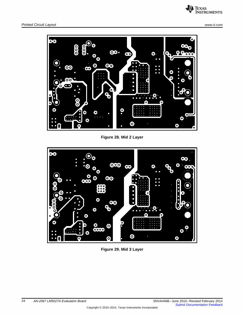
16 Printed Circuit Layout
Figure 24. Top Assembly Layer
Figure 25. Bottom Layer
22 AN-2067 LM5027A Evaluation Board SNVA446B–June 2010–Revised February 2014Submit Documentation Feedback
Copyright © 2010–2014, Texas Instruments Incorporated

www.ti.com Printed Circuit Layout
Figure 26. Bottom Silk Layer
Figure 27. Mid 1 Layer
23SNVA446B–June 2010–Revised February 2014 AN-2067 LM5027A Evaluation BoardSubmit Documentation Feedback
Copyright © 2010–2014, Texas Instruments Incorporated
Printed Circuit Layout www.ti.com
Figure 28. Mid 2 Layer
Figure 29. Mid 3 Layer
24 AN-2067 LM5027A Evaluation Board SNVA446B–June 2010–Revised February 2014Submit Documentation Feedback
Copyright © 2010–2014, Texas Instruments Incorporated

www.ti.com Printed Circuit Layout
Figure 30. Mid 4 Layer
Figure 31. Bottom Assembly Layer
25SNVA446B–June 2010–Revised February 2014 AN-2067 LM5027A Evaluation BoardSubmit Documentation Feedback
Copyright © 2010–2014, Texas Instruments Incorporated

Printed Circuit Layout www.ti.com
Figure 32. Top Layer
Figure 33. Top Silk Layer
26 AN-2067 LM5027A Evaluation Board SNVA446B–June 2010–Revised February 2014Submit Documentation Feedback
Copyright © 2010–2014, Texas Instruments Incorporated

www.ti.com Application Schematic
17 Application Schematic
Figure 34. Application Schematic: Input 36-76, Voutput 6.3 A, 30 A
27SNVA446B–June 2010–Revised February 2014 AN-2067 LM5027A Evaluation BoardSubmit Documentation Feedback
Copyright © 2010–2014, Texas Instruments Incorporated

Revision History www.ti.com
Revision History
Changes from A Revision (May 2013) to B Revision ...................................................................................................... Page
• Changed Top Layer Assy to Bottom Assy, since Top was in twice. ............................................................. 22
NOTE: Page numbers for previous revisions may differ from page numbers in the current version.
28 Revision History SNVA446B–June 2010–Revised February 2014Submit Documentation Feedback
Copyright © 2010–2014, Texas Instruments Incorporated

STANDARD TERMS AND CONDITIONS FOR EVALUATION MODULES1. Delivery: TI delivers TI evaluation boards, kits, or modules, including any accompanying demonstration software, components, or
documentation (collectively, an “EVM” or “EVMs”) to the User (“User”) in accordance with the terms and conditions set forth herein.Acceptance of the EVM is expressly subject to the following terms and conditions.1.1 EVMs are intended solely for product or software developers for use in a research and development setting to facilitate feasibility
evaluation, experimentation, or scientific analysis of TI semiconductors products. EVMs have no direct function and are notfinished products. EVMs shall not be directly or indirectly assembled as a part or subassembly in any finished product. Forclarification, any software or software tools provided with the EVM (“Software”) shall not be subject to the terms and conditionsset forth herein but rather shall be subject to the applicable terms and conditions that accompany such Software
1.2 EVMs are not intended for consumer or household use. EVMs may not be sold, sublicensed, leased, rented, loaned, assigned,or otherwise distributed for commercial purposes by Users, in whole or in part, or used in any finished product or productionsystem.
2 Limited Warranty and Related Remedies/Disclaimers:2.1 These terms and conditions do not apply to Software. The warranty, if any, for Software is covered in the applicable Software
License Agreement.2.2 TI warrants that the TI EVM will conform to TI's published specifications for ninety (90) days after the date TI delivers such EVM
to User. Notwithstanding the foregoing, TI shall not be liable for any defects that are caused by neglect, misuse or mistreatmentby an entity other than TI, including improper installation or testing, or for any EVMs that have been altered or modified in anyway by an entity other than TI. Moreover, TI shall not be liable for any defects that result from User's design, specifications orinstructions for such EVMs. Testing and other quality control techniques are used to the extent TI deems necessary or asmandated by government requirements. TI does not test all parameters of each EVM.
2.3 If any EVM fails to conform to the warranty set forth above, TI's sole liability shall be at its option to repair or replace such EVM,or credit User's account for such EVM. TI's liability under this warranty shall be limited to EVMs that are returned during thewarranty period to the address designated by TI and that are determined by TI not to conform to such warranty. If TI elects torepair or replace such EVM, TI shall have a reasonable time to repair such EVM or provide replacements. Repaired EVMs shallbe warranted for the remainder of the original warranty period. Replaced EVMs shall be warranted for a new full ninety (90) daywarranty period.
3 Regulatory Notices:3.1 United States
3.1.1 Notice applicable to EVMs not FCC-Approved:This kit is designed to allow product developers to evaluate electronic components, circuitry, or software associated with the kitto determine whether to incorporate such items in a finished product and software developers to write software applications foruse with the end product. This kit is not a finished product and when assembled may not be resold or otherwise marketed unlessall required FCC equipment authorizations are first obtained. Operation is subject to the condition that this product not causeharmful interference to licensed radio stations and that this product accept harmful interference. Unless the assembled kit isdesigned to operate under part 15, part 18 or part 95 of this chapter, the operator of the kit must operate under the authority ofan FCC license holder or must secure an experimental authorization under part 5 of this chapter.3.1.2 For EVMs annotated as FCC – FEDERAL COMMUNICATIONS COMMISSION Part 15 Compliant:
CAUTIONThis device complies with part 15 of the FCC Rules. Operation is subject to the following two conditions: (1) This device may notcause harmful interference, and (2) this device must accept any interference received, including interference that may causeundesired operation.Changes or modifications not expressly approved by the party responsible for compliance could void the user's authority tooperate the equipment.
FCC Interference Statement for Class A EVM devicesNOTE: This equipment has been tested and found to comply with the limits for a Class A digital device, pursuant to part 15 ofthe FCC Rules. These limits are designed to provide reasonable protection against harmful interference when the equipment isoperated in a commercial environment. This equipment generates, uses, and can radiate radio frequency energy and, if notinstalled and used in accordance with the instruction manual, may cause harmful interference to radio communications.Operation of this equipment in a residential area is likely to cause harmful interference in which case the user will be required tocorrect the interference at his own expense.
SPACER
SPACER
SPACER
SPACER
SPACER
SPACER
SPACER
SPACER

FCC Interference Statement for Class B EVM devicesNOTE: This equipment has been tested and found to comply with the limits for a Class B digital device, pursuant to part 15 ofthe FCC Rules. These limits are designed to provide reasonable protection against harmful interference in a residentialinstallation. This equipment generates, uses and can radiate radio frequency energy and, if not installed and used in accordancewith the instructions, may cause harmful interference to radio communications. However, there is no guarantee that interferencewill not occur in a particular installation. If this equipment does cause harmful interference to radio or television reception, whichcan be determined by turning the equipment off and on, the user is encouraged to try to correct the interference by one or moreof the following measures:
• Reorient or relocate the receiving antenna.• Increase the separation between the equipment and receiver.• Connect the equipment into an outlet on a circuit different from that to which the receiver is connected.• Consult the dealer or an experienced radio/TV technician for help.
3.2 Canada3.2.1 For EVMs issued with an Industry Canada Certificate of Conformance to RSS-210
Concerning EVMs Including Radio Transmitters:This device complies with Industry Canada license-exempt RSS standard(s). Operation is subject to the following two conditions:(1) this device may not cause interference, and (2) this device must accept any interference, including interference that maycause undesired operation of the device.
Concernant les EVMs avec appareils radio:Le présent appareil est conforme aux CNR d'Industrie Canada applicables aux appareils radio exempts de licence. L'exploitationest autorisée aux deux conditions suivantes: (1) l'appareil ne doit pas produire de brouillage, et (2) l'utilisateur de l'appareil doitaccepter tout brouillage radioélectrique subi, même si le brouillage est susceptible d'en compromettre le fonctionnement.
Concerning EVMs Including Detachable Antennas:Under Industry Canada regulations, this radio transmitter may only operate using an antenna of a type and maximum (or lesser)gain approved for the transmitter by Industry Canada. To reduce potential radio interference to other users, the antenna typeand its gain should be so chosen that the equivalent isotropically radiated power (e.i.r.p.) is not more than that necessary forsuccessful communication. This radio transmitter has been approved by Industry Canada to operate with the antenna typeslisted in the user guide with the maximum permissible gain and required antenna impedance for each antenna type indicated.Antenna types not included in this list, having a gain greater than the maximum gain indicated for that type, are strictly prohibitedfor use with this device.
Concernant les EVMs avec antennes détachablesConformément à la réglementation d'Industrie Canada, le présent émetteur radio peut fonctionner avec une antenne d'un type etd'un gain maximal (ou inférieur) approuvé pour l'émetteur par Industrie Canada. Dans le but de réduire les risques de brouillageradioélectrique à l'intention des autres utilisateurs, il faut choisir le type d'antenne et son gain de sorte que la puissance isotroperayonnée équivalente (p.i.r.e.) ne dépasse pas l'intensité nécessaire à l'établissement d'une communication satisfaisante. Leprésent émetteur radio a été approuvé par Industrie Canada pour fonctionner avec les types d'antenne énumérés dans lemanuel d’usage et ayant un gain admissible maximal et l'impédance requise pour chaque type d'antenne. Les types d'antennenon inclus dans cette liste, ou dont le gain est supérieur au gain maximal indiqué, sont strictement interdits pour l'exploitation del'émetteur
3.3 Japan3.3.1 Notice for EVMs delivered in Japan: Please see http://www.tij.co.jp/lsds/ti_ja/general/eStore/notice_01.page 日本国内に
輸入される評価用キット、ボードについては、次のところをご覧ください。http://www.tij.co.jp/lsds/ti_ja/general/eStore/notice_01.page
3.3.2 Notice for Users of EVMs Considered “Radio Frequency Products” in Japan: EVMs entering Japan may not be certifiedby TI as conforming to Technical Regulations of Radio Law of Japan.
If User uses EVMs in Japan, not certified to Technical Regulations of Radio Law of Japan, User is required by Radio Law ofJapan to follow the instructions below with respect to EVMs:1. Use EVMs in a shielded room or any other test facility as defined in the notification #173 issued by Ministry of Internal
Affairs and Communications on March 28, 2006, based on Sub-section 1.1 of Article 6 of the Ministry’s Rule forEnforcement of Radio Law of Japan,
2. Use EVMs only after User obtains the license of Test Radio Station as provided in Radio Law of Japan with respect toEVMs, or
3. Use of EVMs only after User obtains the Technical Regulations Conformity Certification as provided in Radio Law of Japanwith respect to EVMs. Also, do not transfer EVMs, unless User gives the same notice above to the transferee. Please notethat if User does not follow the instructions above, User will be subject to penalties of Radio Law of Japan.
SPACER
SPACER
SPACER
SPACER
SPACER

【無線電波を送信する製品の開発キットをお使いになる際の注意事項】 開発キットの中には技術基準適合証明を受けていないものがあります。 技術適合証明を受けていないもののご使用に際しては、電波法遵守のため、以下のいずれかの措置を取っていただく必要がありますのでご注意ください。1. 電波法施行規則第6条第1項第1号に基づく平成18年3月28日総務省告示第173号で定められた電波暗室等の試験設備でご使用
いただく。2. 実験局の免許を取得後ご使用いただく。3. 技術基準適合証明を取得後ご使用いただく。
なお、本製品は、上記の「ご使用にあたっての注意」を譲渡先、移転先に通知しない限り、譲渡、移転できないものとします。上記を遵守頂けない場合は、電波法の罰則が適用される可能性があることをご留意ください。 日本テキサス・イ
ンスツルメンツ株式会社東京都新宿区西新宿6丁目24番1号西新宿三井ビル
3.3.3 Notice for EVMs for Power Line Communication: Please see http://www.tij.co.jp/lsds/ti_ja/general/eStore/notice_02.page電力線搬送波通信についての開発キットをお使いになる際の注意事項については、次のところをご覧ください。http://www.tij.co.jp/lsds/ti_ja/general/eStore/notice_02.page
SPACER4 EVM Use Restrictions and Warnings:
4.1 EVMS ARE NOT FOR USE IN FUNCTIONAL SAFETY AND/OR SAFETY CRITICAL EVALUATIONS, INCLUDING BUT NOTLIMITED TO EVALUATIONS OF LIFE SUPPORT APPLICATIONS.
4.2 User must read and apply the user guide and other available documentation provided by TI regarding the EVM prior to handlingor using the EVM, including without limitation any warning or restriction notices. The notices contain important safety informationrelated to, for example, temperatures and voltages.
4.3 Safety-Related Warnings and Restrictions:4.3.1 User shall operate the EVM within TI’s recommended specifications and environmental considerations stated in the user
guide, other available documentation provided by TI, and any other applicable requirements and employ reasonable andcustomary safeguards. Exceeding the specified performance ratings and specifications (including but not limited to inputand output voltage, current, power, and environmental ranges) for the EVM may cause personal injury or death, orproperty damage. If there are questions concerning performance ratings and specifications, User should contact a TIfield representative prior to connecting interface electronics including input power and intended loads. Any loads appliedoutside of the specified output range may also result in unintended and/or inaccurate operation and/or possiblepermanent damage to the EVM and/or interface electronics. Please consult the EVM user guide prior to connecting anyload to the EVM output. If there is uncertainty as to the load specification, please contact a TI field representative.During normal operation, even with the inputs and outputs kept within the specified allowable ranges, some circuitcomponents may have elevated case temperatures. These components include but are not limited to linear regulators,switching transistors, pass transistors, current sense resistors, and heat sinks, which can be identified using theinformation in the associated documentation. When working with the EVM, please be aware that the EVM may becomevery warm.
4.3.2 EVMs are intended solely for use by technically qualified, professional electronics experts who are familiar with thedangers and application risks associated with handling electrical mechanical components, systems, and subsystems.User assumes all responsibility and liability for proper and safe handling and use of the EVM by User or its employees,affiliates, contractors or designees. User assumes all responsibility and liability to ensure that any interfaces (electronicand/or mechanical) between the EVM and any human body are designed with suitable isolation and means to safelylimit accessible leakage currents to minimize the risk of electrical shock hazard. User assumes all responsibility andliability for any improper or unsafe handling or use of the EVM by User or its employees, affiliates, contractors ordesignees.
4.4 User assumes all responsibility and liability to determine whether the EVM is subject to any applicable international, federal,state, or local laws and regulations related to User’s handling and use of the EVM and, if applicable, User assumes allresponsibility and liability for compliance in all respects with such laws and regulations. User assumes all responsibility andliability for proper disposal and recycling of the EVM consistent with all applicable international, federal, state, and localrequirements.
5. Accuracy of Information: To the extent TI provides information on the availability and function of EVMs, TI attempts to be as accurateas possible. However, TI does not warrant the accuracy of EVM descriptions, EVM availability or other information on its websites asaccurate, complete, reliable, current, or error-free.
SPACER
SPACER
SPACER
SPACER
SPACER
SPACER

SPACER6. Disclaimers:
6.1 EXCEPT AS SET FORTH ABOVE, EVMS AND ANY WRITTEN DESIGN MATERIALS PROVIDED WITH THE EVM (AND THEDESIGN OF THE EVM ITSELF) ARE PROVIDED "AS IS" AND "WITH ALL FAULTS." TI DISCLAIMS ALL OTHERWARRANTIES, EXPRESS OR IMPLIED, REGARDING SUCH ITEMS, INCLUDING BUT NOT LIMITED TO ANY IMPLIEDWARRANTIES OF MERCHANTABILITY OR FITNESS FOR A PARTICULAR PURPOSE OR NON-INFRINGEMENT OF ANYTHIRD PARTY PATENTS, COPYRIGHTS, TRADE SECRETS OR OTHER INTELLECTUAL PROPERTY RIGHTS.
6.2 EXCEPT FOR THE LIMITED RIGHT TO USE THE EVM SET FORTH HEREIN, NOTHING IN THESE TERMS ANDCONDITIONS SHALL BE CONSTRUED AS GRANTING OR CONFERRING ANY RIGHTS BY LICENSE, PATENT, OR ANYOTHER INDUSTRIAL OR INTELLECTUAL PROPERTY RIGHT OF TI, ITS SUPPLIERS/LICENSORS OR ANY OTHER THIRDPARTY, TO USE THE EVM IN ANY FINISHED END-USER OR READY-TO-USE FINAL PRODUCT, OR FOR ANYINVENTION, DISCOVERY OR IMPROVEMENT MADE, CONCEIVED OR ACQUIRED PRIOR TO OR AFTER DELIVERY OFTHE EVM.
7. USER'S INDEMNITY OBLIGATIONS AND REPRESENTATIONS. USER WILL DEFEND, INDEMNIFY AND HOLD TI, ITSLICENSORS AND THEIR REPRESENTATIVES HARMLESS FROM AND AGAINST ANY AND ALL CLAIMS, DAMAGES, LOSSES,EXPENSES, COSTS AND LIABILITIES (COLLECTIVELY, "CLAIMS") ARISING OUT OF OR IN CONNECTION WITH ANYHANDLING OR USE OF THE EVM THAT IS NOT IN ACCORDANCE WITH THESE TERMS AND CONDITIONS. THIS OBLIGATIONSHALL APPLY WHETHER CLAIMS ARISE UNDER STATUTE, REGULATION, OR THE LAW OF TORT, CONTRACT OR ANYOTHER LEGAL THEORY, AND EVEN IF THE EVM FAILS TO PERFORM AS DESCRIBED OR EXPECTED.
8. Limitations on Damages and Liability:8.1 General Limitations. IN NO EVENT SHALL TI BE LIABLE FOR ANY SPECIAL, COLLATERAL, INDIRECT, PUNITIVE,
INCIDENTAL, CONSEQUENTIAL, OR EXEMPLARY DAMAGES IN CONNECTION WITH OR ARISING OUT OF THESETERMS ANDCONDITIONS OR THE USE OF THE EVMS PROVIDED HEREUNDER, REGARDLESS OF WHETHER TI HASBEEN ADVISED OF THE POSSIBILITY OF SUCH DAMAGES. EXCLUDED DAMAGES INCLUDE, BUT ARE NOT LIMITEDTO, COST OF REMOVAL OR REINSTALLATION, ANCILLARY COSTS TO THE PROCUREMENT OF SUBSTITUTE GOODSOR SERVICES, RETESTING, OUTSIDE COMPUTER TIME, LABOR COSTS, LOSS OF GOODWILL, LOSS OF PROFITS,LOSS OF SAVINGS, LOSS OF USE, LOSS OF DATA, OR BUSINESS INTERRUPTION. NO CLAIM, SUIT OR ACTION SHALLBE BROUGHT AGAINST TI MORE THAN ONE YEAR AFTER THE RELATED CAUSE OF ACTION HAS OCCURRED.
8.2 Specific Limitations. IN NO EVENT SHALL TI'S AGGREGATE LIABILITY FROM ANY WARRANTY OR OTHER OBLIGATIONARISING OUT OF OR IN CONNECTION WITH THESE TERMS AND CONDITIONS, OR ANY USE OF ANY TI EVMPROVIDED HEREUNDER, EXCEED THE TOTAL AMOUNT PAID TO TI FOR THE PARTICULAR UNITS SOLD UNDERTHESE TERMS AND CONDITIONS WITH RESPECT TO WHICH LOSSES OR DAMAGES ARE CLAIMED. THE EXISTENCEOF MORE THAN ONE CLAIM AGAINST THE PARTICULAR UNITS SOLD TO USER UNDER THESE TERMS ANDCONDITIONS SHALL NOT ENLARGE OR EXTEND THIS LIMIT.
9. Return Policy. Except as otherwise provided, TI does not offer any refunds, returns, or exchanges. Furthermore, no return of EVM(s)will be accepted if the package has been opened and no return of the EVM(s) will be accepted if they are damaged or otherwise not ina resalable condition. If User feels it has been incorrectly charged for the EVM(s) it ordered or that delivery violates the applicableorder, User should contact TI. All refunds will be made in full within thirty (30) working days from the return of the components(s),excluding any postage or packaging costs.
10. Governing Law: These terms and conditions shall be governed by and interpreted in accordance with the laws of the State of Texas,without reference to conflict-of-laws principles. User agrees that non-exclusive jurisdiction for any dispute arising out of or relating tothese terms and conditions lies within courts located in the State of Texas and consents to venue in Dallas County, Texas.Notwithstanding the foregoing, any judgment may be enforced in any United States or foreign court, and TI may seek injunctive reliefin any United States or foreign court.
Mailing Address: Texas Instruments, Post Office Box 655303, Dallas, Texas 75265Copyright © 2015, Texas Instruments Incorporated
spacer

IMPORTANT NOTICE
Texas Instruments Incorporated and its subsidiaries (TI) reserve the right to make corrections, enhancements, improvements and otherchanges to its semiconductor products and services per JESD46, latest issue, and to discontinue any product or service per JESD48, latestissue. Buyers should obtain the latest relevant information before placing orders and should verify that such information is current andcomplete. All semiconductor products (also referred to herein as “components”) are sold subject to TI’s terms and conditions of salesupplied at the time of order acknowledgment.TI warrants performance of its components to the specifications applicable at the time of sale, in accordance with the warranty in TI’s termsand conditions of sale of semiconductor products. Testing and other quality control techniques are used to the extent TI deems necessaryto support this warranty. Except where mandated by applicable law, testing of all parameters of each component is not necessarilyperformed.TI assumes no liability for applications assistance or the design of Buyers’ products. Buyers are responsible for their products andapplications using TI components. To minimize the risks associated with Buyers’ products and applications, Buyers should provideadequate design and operating safeguards.TI does not warrant or represent that any license, either express or implied, is granted under any patent right, copyright, mask work right, orother intellectual property right relating to any combination, machine, or process in which TI components or services are used. Informationpublished by TI regarding third-party products or services does not constitute a license to use such products or services or a warranty orendorsement thereof. Use of such information may require a license from a third party under the patents or other intellectual property of thethird party, or a license from TI under the patents or other intellectual property of TI.Reproduction of significant portions of TI information in TI data books or data sheets is permissible only if reproduction is without alterationand is accompanied by all associated warranties, conditions, limitations, and notices. TI is not responsible or liable for such altereddocumentation. Information of third parties may be subject to additional restrictions.Resale of TI components or services with statements different from or beyond the parameters stated by TI for that component or servicevoids all express and any implied warranties for the associated TI component or service and is an unfair and deceptive business practice.TI is not responsible or liable for any such statements.Buyer acknowledges and agrees that it is solely responsible for compliance with all legal, regulatory and safety-related requirementsconcerning its products, and any use of TI components in its applications, notwithstanding any applications-related information or supportthat may be provided by TI. Buyer represents and agrees that it has all the necessary expertise to create and implement safeguards whichanticipate dangerous consequences of failures, monitor failures and their consequences, lessen the likelihood of failures that might causeharm and take appropriate remedial actions. Buyer will fully indemnify TI and its representatives against any damages arising out of the useof any TI components in safety-critical applications.In some cases, TI components may be promoted specifically to facilitate safety-related applications. With such components, TI’s goal is tohelp enable customers to design and create their own end-product solutions that meet applicable functional safety standards andrequirements. Nonetheless, such components are subject to these terms.No TI components are authorized for use in FDA Class III (or similar life-critical medical equipment) unless authorized officers of the partieshave executed a special agreement specifically governing such use.Only those TI components which TI has specifically designated as military grade or “enhanced plastic” are designed and intended for use inmilitary/aerospace applications or environments. Buyer acknowledges and agrees that any military or aerospace use of TI componentswhich have not been so designated is solely at the Buyer's risk, and that Buyer is solely responsible for compliance with all legal andregulatory requirements in connection with such use.TI has specifically designated certain components as meeting ISO/TS16949 requirements, mainly for automotive use. In any case of use ofnon-designated products, TI will not be responsible for any failure to meet ISO/TS16949.
Products ApplicationsAudio www.ti.com/audio Automotive and Transportation www.ti.com/automotiveAmplifiers amplifier.ti.com Communications and Telecom www.ti.com/communicationsData Converters dataconverter.ti.com Computers and Peripherals www.ti.com/computersDLP® Products www.dlp.com Consumer Electronics www.ti.com/consumer-appsDSP dsp.ti.com Energy and Lighting www.ti.com/energyClocks and Timers www.ti.com/clocks Industrial www.ti.com/industrialInterface interface.ti.com Medical www.ti.com/medicalLogic logic.ti.com Security www.ti.com/securityPower Mgmt power.ti.com Space, Avionics and Defense www.ti.com/space-avionics-defenseMicrocontrollers microcontroller.ti.com Video and Imaging www.ti.com/videoRFID www.ti-rfid.comOMAP Applications Processors www.ti.com/omap TI E2E Community e2e.ti.comWireless Connectivity www.ti.com/wirelessconnectivity
Mailing Address: Texas Instruments, Post Office Box 655303, Dallas, Texas 75265Copyright © 2015, Texas Instruments Incorporated


![AK7734 Evaluation Board Rev - AKM Evaluation Board Rev.1 AKD7734-A [AKD7734-A] 2011/07 - 2 - Evaluation Board Diagram Board Diagram +12V-12V](https://img.pdfslide.us/doc/110x75/5c03e45309d3f203258d6861/ak7734-evaluation-board-rev-akm-evaluation-board-rev1-akd7734-a-akd7734-a-201107.jpg)

![Issue - 4th Edition Shrawan 2067]](https://img.pdfslide.us/doc/110x75/568bd4ec1a28ab20349695ae/issue-4th-edition-shrawan-2067.jpg)