Embed Size (px)
Citation preview

Application ReportSNVA419C–April 2010–Revised April 2013
AN-2020 Thermal Design By Insight, Not Hindsight.....................................................................................................................................................
ABSTRACT
This application report provides an in-depth discussion of thermal design.
Contents1 Introduction .................................................................................................................. 22 Definitions .................................................................................................................... 2
2.1 Example: Calculating Your Required θJA ........................................................................ 53 Rules of Thumb ............................................................................................................. 5
3.1 Rule 1: Board Size ................................................................................................. 53.2 Rule 2: Thermal VIAS ............................................................................................. 63.3 Rule 3: Copper Thickness ........................................................................................ 73.4 Rule 4: Avoid Breaks in the Thermal Path ...................................................................... 73.5 Rule 5: Heat Sink Placement is Just as Important as Selection ............................................. 83.6 Rule 6: Multiple Heat Sources: Superposition Almost Works ................................................ 9
4 Summary ..................................................................................................................... 95 Derivation of Rule 1 (Thermal Resistance from the Surface of the PCB to Ambient Air) ......................... 96 References ................................................................................................................. 11
List of Figures
1 IC Mounted On A Four-Layer Printed Circuit Board.................................................................... 2
2 Simplified Thermal Resistance Model For A Typical PCB............................................................. 3
3 Expanded Thermal Resistance Model For A Typical PCB ........................................................... 4
4 A Hot Spot Is Created When A Break Is Created In The Thermal Path............................................. 8
5 Thermal Resistance Model With Heat Sink Attached To The Package Top ........................................ 8
6 Thermal Resistance Model With Heat Sink Attached To Board Bottom............................................. 9
List of Tables
1 Typical Thermal Resistance Values ...................................................................................... 4
2 Calculating Coefficienct Of Heat Transfer Using Grashof Number. Used For Natural ConvectionCalculations ................................................................................................................ 11
All trademarks are the property of their respective owners.
1SNVA419C–April 2010–Revised April 2013 AN-2020 Thermal Design By Insight, Not HindsightSubmit Documentation Feedback
Copyright © 2010–2013, Texas Instruments Incorporated

TJA =Power Dissipation
TJUNCTION - TAMBIENT
Top Copper Layer
Inner Ground Layer
Second Inner Layer
Bottom Ground Layer
Exposed Pad (EP)
EP Landing Pattern
12 mil diameter
Thermal Vias
Silicon Die (Junction)
Package Body
1.6 mm r 10%
2 oz/ft2
(0.070 mm)
1 oz/ft2
(0.035 mm)
1 oz/ft2
(0.035 mm)
2 oz/ft2
(0.070 mm)
Introduction www.ti.com
1 Introduction
All electronics contain semiconductor devices, capacitors and other components that are vulnerable tothermally accelerated failure mechanisms. Thermal design becomes vital to improving the reliability of anydesign. Unfortunately, thermal design can be very difficult because of the mathematical analysis of fluiddynamics for complex geometries. Although this remains true for the foreseeable future, this applicationreport covers the basics of thermal design for DC-DC converters using a simplified resistor model of heattransfer. Focus is on the thermal design for the semiconductor devices, but all of these techniques can beapplied to other components. The resistor model is very useful for quickly estimating your designrequirements, such as the PCB size and whether airflow is required. Finite element analysis software canthen be used to analyze the design in more detail. The listed reference material is home to additional dataand many useful thermal calculators, covering material that is beyond the scope of this document.
Our discussion of thermal design will begin with the definition of parameters used in data sheets such asθJA and θJC, and end with some rules of thumb for the thermal design of a DC-DC converter, including theirderivation. An accompanying spreadsheet (see References) uses these derivations to quickly provide aballpark figure for the thermal performance of your design.
2 Definitions
Description of Thermal Terms
Parameters of interest : θJA, θJC, θCA, θJT
Figure 1. IC Mounted On A Four-Layer Printed Circuit Board
The most commonly specified parameter, in data sheets, for thermal performance is θJA. θJA is defined asthe thermal impedance from the Junction, of the integrated circuit under test, to the Ambient environment.If we describe it using a resistor model, it is the parallel combination of all the paths that heat can take tomove from the IC junction to the ambient air. The equation for this thermal resistance is:
(1)
In our resistor model the heat transfer, measured in watts, takes the place of charge transfer measured inamps, and the temperature potential between the junction and ambient temperatures replaces the voltagepotential. The heat that needs to be transferred away from the junction is the power dissipated by the IC.
2 AN-2020 Thermal Design By Insight, Not Hindsight SNVA419C–April 2010–Revised April 2013Submit Documentation Feedback
Copyright © 2010–2013, Texas Instruments Incorporated

Case Top Temperature
(TT)
Junction Temperature
(TJ)
Exposed Pad/Case Temperature
(TC)
Ambient Air Temperature
(TA) TT
TJ
TC
TA
TAJT
JC CA
JA
TJ TA
www.ti.com Definitions
Figure 2. Simplified Thermal Resistance Model For A Typical PCB
There are two primary heat paths for a DC-DC converter represented above by their associated thermalresistances. The first path travels from the junction of the IC to the plastic molding at the top of the case(θJT) and then to the ambient air by convection/radiation (θTA). The second path is from the junction of theIC to an exposed pad (θJC). The exposed pad is then connected to the PCB, where the heat travels to thesurface of the PCB and to the ambient air by convection/radiation (θCA).
There is one point of confusion that is common in defining θJC.
For DC-DC converters without an exposed pad, θJC is defined as the thermal impedance from the junctionto the top of the case. This is in direct conflict with our previous definition of θJC, being the thermalimpedance from the junction to the exposed pad. This confusion comes about because of the largenumber of packages that DC-DC converters have been shoved into over the years. As newer packageswith exposed pads were released into the market it was decided that θJC should represent the lowestthermal impedance path from the junction of the IC to the outside world.
Now that we have cleared up the terminology, we can discuss the usefulness of various parameters.
Use the value of θJA given in the data sheet to compare different packages, and use it along with the ICpower dissipation for a sanity check in your design. The high thermal resistance of the plastic packagingensures that most of the heat travels from the exposed copper pad to the PCB, which usually has a muchlower thermal resistance. A heat sink can be added to either the top of the package or directly beneath theexposed pad on the backside of the PCB. Again, because of the high thermal resistance of plastic, a heatsink will be more effective when connected to an exposed metal pad, either directly or, through thermalvias.
Since most of the heat transfer is through the exposed pad to the PCB it becomes immediately apparentthat the value of θJA is highly PCB dependant. In other words, the most critical value to determine in anydesign is thermal resistance of the PCB (θCA). Well what, exactly, is θCA and how is it calculated? θCA is theequivalent resistance of a thermal resistive lattice that centers on the IC and ends at the surfaces of theboard. It is the final of your freshman year, Circuits 101 class, all over again. Figure 3 below shows thedetails.
3SNVA419C–April 2010–Revised April 2013 AN-2020 Thermal Design By Insight, Not HindsightSubmit Documentation Feedback
Copyright © 2010–2013, Texas Instruments Incorporated

TFR4 = = Area
x Thickness
1 cm x 1 cm
x 0.032 cm435°C cm
W1èFR4
TSA = =Surface Area 1 cm x 1 cm
1000°C cm 2
W1h
TVIA =Area
x Length1OCu
=S x [(0.01524 cm)2 - (0.01524 cm-0.00175 cm)2]
x 0.165 cm0.25°C cm W
TCu = = Area
x Length
1 cm x .0035 cm
x 1 cm0.25°C cm
W1èCu
TC
Ambient Air Temperature
(TA)
Junction Temperature
TJ __
VIA
SA SA
SA SASASASASA
SASAJC
Cu
Cu
Cu
Cu
Cu
Cu
FR4
FR4
FR4
FR4
FR4
FR4
Cu
FR4
FR4
FR4
FR4
FR4
FR4
Cu
Cu
Cu
Cu
Cu
Cu
Cu
Cu
Cu
Cu
Definitions www.ti.com
Figure 3. Expanded Thermal Resistance Model For A Typical PCB
There are new terms to add to our ever growing lexicon of θ's. θCu is the thermal resistance of our board'scopper to lateral heat transfer. θFR4 is the thermal resistance between the copper planes provided by thevertical resistance of FR-4 laminate. θVIA is the thermal resistance of the thermal vias placed directlyunderneath the exposed pad. θSA is the thermal resistance from the surface of the PCB to the ambient air.It is a combination of convective and radiative heat transfer. If we break the board into 1 cm squares, thetypical values for these resistances are listed below.
Table 1. Typical Thermal Resistance Values
Nam Value Description Conditions Equatione
θCu 71.4 °C / Lateral thermal Length = 1 cm, width = 1 cm,W resistance of 1 ounce copper thickness =
copper plane. 0.0035 cm, thermalconductivity of copper (λCu) = (2)4 W / (cm °C)
θVIA 261 °C / W Thermal Via length = 0.165 cm (65resistance of mils), 0.5 ounce coppertypical 12 mil plating thickness = 0.00175via. cm, drill hole radius = 6 mil
(0.01524 cm), thermalconductivity of copper (λCu) =4 W / (cm °C)
(3)
θSA 1000 °C / Thermal 1 cm square, a first orderW resistance from approximation of the heat
the surface of a transfer coefficient of PCB(4)1 cm square of Board to Air for natural
the PCB to the convection is (h) = 0.001 W /ambient air due (cm2 °C)to naturalconvection.
θFR4 13.9 °C / Vertical thermal 1 cm square, FR-4 thicknessW resistance of = 0. 032 cm (12.6 mil),
FR-4 substrate. thermal conductivity of FR-4(λFR4) = 0.0023 W / (cm °C) (5)
4 AN-2020 Thermal Design By Insight, Not Hindsight SNVA419C–April 2010–Revised April 2013Submit Documentation Feedback
Copyright © 2010–2013, Texas Instruments Incorporated

Board Area (cm2)��8 15.29
Board Area (in2)��8 2.37
x PD
x PD
Wcm2
Win2
TJA 70.94W
90°C - 50°C7 42.5 °C/W
PD = = 0.94W2.5V x 4A x ( -1)10.914
PD = VOUT x IOUT x ( -1)1�
www.ti.com Rules of Thumb
The amount of variability in PCB designs is significant. You can see that the thermal resistance dependson board size, airflow, PCB thickness and many other parameters. For this reason, a series of JEDECstandards (JESD51-1 to JESD51-11) were developed, which specify the PCB size and layout for testingθJA for different types of packages. DC-DC converters that are tested to these standards can be directlycompared to one another. Always check the data sheet to see what PCB parameters were used tomeasure θJA. Later on we will discuss some tips for designing your PCB, but the final design, and thus θJA,depends on the end user.
2.1 Example: Calculating Your Required θJA
Calculate the θJA required for a DC-DC converter with an output voltage, VOUT, of 2.5V and output current,IOUT, of 4 amperes. The converter efficiency, η, is 91.4%. The ambient temperature, TA, is 50°C. Thecapacitors you selected are rated up to 100°C, and because of their proximity to the DC-DC converter youdecide that the maximum junction temperature, TJ, you would like the converter to reach is 90°C.
The power dissipated by the converter, PD, can be easily calculated.
(6)
(7)
Assuming that all of the power is dissipated internally to the IC, (a fair assumption if using LDOs ormodules) we can now calculate the maximum value of θJA.
(8)
Since a θJA of less than 42.5°C / Watt is required for your design, you won’t get there with a SOT-23 whichhas a θJA closer to 179°C / Watt. You would need to select a package like the 14 Pin eMSOP with a θJA ofaround 40°C / W. If you would like to increase the thermal margins for your design, pick a package like theTO-PMOD-7 or TO-263, which have θJA's of around 20°C / W. Remember θJA is board dependant and allof these numbers come from using a JEDEC standard test board measuring 3” x 4”. If your board variesfrom the JEDEC board, which it will, you will need to get a better estimate of thermal performance byusing θJC, and deriving θCA.
A package with a low θJC will have very good heat transfer to the case, usually to an exposed pad. θJC is avery good indicator of a packages thermal performance. A low value for θJA implies a low value for θJC.The θJC for packages designed to dissipate large amounts of power can be less than 2°C / Watt. Typically,packages with no exposed pad have a θJC of greater than 100°C / Watt. That means that for every wattdissipated in the package the temperature difference between the junction of the IC and case will increase100°C. If the value of θJC is not included in the data sheet it can often be requested from the manufacturer.
3 Rules of Thumb
PCB DESIGN to meet a given θCA
Parameters of interest: θCA
A low value for θJC (less than 10 °C / Watt) is a good start for a thermal design, but we still need to designa PCB or heat sink to transfer the heat from the case to the ambient air. This section will provide simpleguidelines so that we can avoid calculating the full resistor model. The derivations for these rules of thumbwill be discussed later.
3.1 Rule 1: Board Size
a)
(9)
5SNVA419C–April 2010–Revised April 2013 AN-2020 Thermal Design By Insight, Not HindsightSubmit Documentation Feedback
Copyright © 2010–2013, Texas Instruments Incorporated

åVIAS �# of Thermal Vias
261°C W
Board Area (in2) 842.5
77.5 °C x in 2 W
- 1.9°CW
°CW
= 1.91 in2
Board Area (in2) 8 = 2.2 in277.5 °C x in 2
W
42.5 - 7.3°CW
°CW
Board Area (in2) 8 = 2.23 in2in2 W2.37 x 0.94W
Board Area (in2) 877.5°C x in 2
W�JA - �JC
Board Area (cm2) 8500°C x cm 2
W�JA - �JC
Rules of Thumb www.ti.com
With only natural convection (i.e. no airflow), and no heat sink, a typical two sided PCB with solid copperfills on both sides, needs at least 15.29 cm2 (≊ 2.37 in2) of area to dissipate 1 watt of power for a 40°C risein temperature. Adding airflow can typically reduce this size requirement by up to half. To reduce boardarea further a heat sink will be required.
Several assumptions are made here. First, that any enclosure for the PCB does not restrict the naturalconvection of either side of the PCB. Second, that the PCB provides a low thermal resistance from the ICto the edges of the board. This can be accomplished by attaching the exposed pad to copper groundplanes that extend to the edge of the PCB. With a four layer board, the internal ground planes can also beused to transfer the heat to the edges of the board. This can improve the thermal performance of even awell designed two-layer board by up to 30 percent.
b) The following equation can be used to approximate the minimum board size if θJC is known.
(10)
where θJC is obtained from the datsheet, and θJA is calculated from the power dissipation, ambienttemperature, and maximum junction temperature as shown in the previous example.
3.1.1 Example: Calculating the Required Board Size to Hit a Target θJA
Using our previous DC-DC converter example with VOUT = 2.5, IOUT = 4A, and PD = 0.94W, we determinedthat a θJA = 42.5°C / W was necessary for the design.
a) Using the rule of thumb, with no airflow the PCB should be at least
(11)
b) Compare this to the equation using θJC. We determined that a 14 pin eMSOP would be a good choicefor this design because the θJA is around 40°C / W on the JEDEC board. A 14 pin eMSOP has a θJC of ≊7.3°C / W. Using the equation we can calculate a minimum PCB area
(12)
If we had picked a package that was not suitable to the task such a SOT-23 with a θJC ≊ 100°C / W, theanswer would be negative telling us that there is no amount of board area that could be used to heat sinkthis device and meet the specifications.
However, if we had picked the TO-PMOD-7 package with θJC ≊ 1.9°C / W we could have reduced theboard size, or gained some margin for our design.
(13)
3.2 Rule 2: Thermal VIAS
(14)
A typical 12 mil diameter thru hole via with 0.5 oz copper sidewalls has a thermal resistance of 261 °C /Watt. Place as many thermal vias as will fit underneath the exposed pad to form an array, with 1mmspacing. Connect the vias to as many layers of copper as possible to spread the heat away from thepackage and to the PCB surface where it can transfer to the ambient air. For many DC-DC converters theexposed pad is electrically connected to ground and thus, the internal ground layer and the bottom groundlayer are usually the most convenient copper planes for heat transfer. The thermal resistance issignificantly lowered by having as solid a bottom layer ground as possible.
6 AN-2020 Thermal Design By Insight, Not Hindsight SNVA419C–April 2010–Revised April 2013Submit Documentation Feedback
Copyright © 2010–2013, Texas Instruments Incorporated

TCu = Width x Thickness
x Length1OCu
TVIA =S x [(radius)2 - (radius ± plating thickness)2]
x Length1OCu
www.ti.com Rules of Thumb
The thermal resistance of a via can be calculated using the following equation
(15)
where λCu = 4 W / cm K, the length is the thickness of the board (0.1561 cm typ), the radius is the radiusof the drill hole (0.1524 cm typ), and the plating thickness = 0.0035 cm multiplied by the copper weight inounces.
3.2.1 Example: Thermal Impedance of VIA Array
Using the 14-pin eMSOP. The exposed pad measures 3.1 x 3.2 mm. This would allow us to fit 16 thermalvias underneath the exposed pad of the device using 1mm spacing. Connect the vias to the copperground layers to spread the heat. The thermal resistance of this 4 x4 array would be approximately 261 /16 = 16.3°C / W
There are many advocates of completely plating closed the thermal vias to improve the thermalperformance. A typical 8 mil diameter plated closed via has a thermal resistance of 128°C / W. Thethermal resistance of the 16 vias in parallel is 128 / 16 = 8°C / W. The improvement in heat transfer to thebottom of the package is considerable, but it is usually not worth the cost. Plating closed the thermal viascan double or triple the cost of your PCB design. A more economical option is to ask for 1 oz plating onstandard 12 mil vias, with perhaps a 10-20% cost adder. The thermal resistance of a single via is reducedto 140°C / W, and for a 4 x 4 array the thermal resistance is only 8.75°C / W.
Another option is to use a package with a larger exposed pad such as the TO-PMOD-7. The exposed padmeasures 5.35 mm x 8.54 mm. This would allow us to place at least 40 vias. The thermal resistance ofthe via array using standard 12 mil vias is only 261 / 40 = 6.525°C / W.
3.3 Rule 3: Copper Thickness
The thicker the copper in the board, the more easily heat can transfer away from the IC. The equation forthe thermal resistance of a copper plane to lateral heat transfer is
(16)
where λCu = 4 W / cm K, Length and Width are in centimeters, and copper Thickness = 0.0035 cmmultiplied by the copper weight in ounces (0.5 oz. typical).
At least one ounce copper is recommended for all DC-DC converter designs. Two ounce copper isrecommended for designs that dissipate more than 3 watts. Four ounce copper is recommended fordesigns that dissipate more than 6 watts.
To truly appreciate the value of thicker copper in a design we will look at the results for two "almost"identical two layer boards. The only difference is in the thickness of the copper. The first board has oneounce copper, and the second board has two ounce copper. Both boards measure 3 x 3" with minimalcopper on the top layer where the component is placed, and the bottom layer completely filled with copperas a heat spreader. θJA = 28.3°C / W for the first board and 21.2°C / W for the board with thicker copper.This is a 25% improvement in the thermal performance of the board, by only changing the copper weight.
3.4 Rule 4: Avoid Breaks in the Thermal Path
Maintain a copper ground plane on either the top or bottom copper layer with as few breaks as possible tocreate a heat spreader on the PCB. Spreading the heat across the PCB provides a low impedance path tothe surface of the PCB and improves convective heat transfer. Traces perpendicular to the heat flow willcreate high impedances (speed bumps) for the heat and create hot spots (traffic jams). If traces throughthe copper heat spreader are unavoidable try to make them run parallel to the heat transfer, which flowsradially from the heat source. The thermal image below Figure 4 shows three almost identical boards withthe same power dissipation. The only difference is a wide cut made on the top copper that breaks thethermal path. In the middle board, where the break is perpendicular to the heat flow this causes a 5.5 °Crise in temperature on an otherwise identical board. On the right hand board, where the break is parallel tothe heat flow, the temperature rise is only 1.5 °C. This might make a serious difference if the board ispushing the thermal limits of the design.
7SNVA419C–April 2010–Revised April 2013 AN-2020 Thermal Design By Insight, Not HindsightSubmit Documentation Feedback
Copyright © 2010–2013, Texas Instruments Incorporated

Case Top Temperature
(TT)
Junction Temperature
(TJ)
Exposed Pad/Case Temperature
(TC)
Ambient Air Temperature
(TA)
TT
TJ
TC
TA
TAJT
JC CA
JA
TJ TA
Heat Sink Temperature
(THS)
HEATSIN
K
Rules of Thumb www.ti.com
Figure 4. A Hot Spot Is Created When A Break Is Created In The Thermal Path
3.5 Rule 5: Heat Sink Placement is Just as Important as Selection
Heat sink selection must include the thermal resistance from the IC junction to the attachment point of theheat sink to be effective. For best performance a heat sink should be attached to the lowest impedancepath to the IC junction.
3.5.1 Example: Heat Sink Performance for Different Locations
To understand rule 5 we will take a look at heat sink performance at two locations. If we again look at theTO-PMOD7, the package has a very low θJC = 1.35 °C / W. The thermal resistance to the top of thepackage is considerably higher because of the plastic interface. θJT can range from 50 to 200 °C / W forpackages with a plastic top. A heat sink on top of the package is connected in series with the high thermalimpedance of the plastic making the heat sink less effective. A heat sink on the bottom of the board isconnected in series with the low thermal impedance of the exposed pad and the relatively low thermalimpedance of the vias making the heat sink more effective. To determine the effectiveness of a heat sinkat the two locations, let's compare the resistive models.
Figure 5. Thermal Resistance Model With Heat Sink Attached To The Package Top
8 AN-2020 Thermal Design By Insight, Not Hindsight SNVA419C–April 2010–Revised April 2013Submit Documentation Feedback
Copyright © 2010–2013, Texas Instruments Incorporated

TSA = =0.1 1550 in2
Surface Area
h Wm2 K
x1 m2
=Surface
Area
1 155W
in2 K
Surface Area
Case Top Temperature
(TT)
Junction Temperature
(TJ)
Exposed Pad/Case Temperature
(TC)
Ambient Air Temperature
(TA) TT
TJ
TC
TA
TAJT
JC CA
JA
TJ TA
Heat Sink Temperature
(THS)
VIASHEATSIN
K
www.ti.com Summary
Figure 6. Thermal Resistance Model With Heat Sink Attached To Board Bottom
Newer MOSFET packages are improving the thermal conductivity to the top of the package by having anexposed metal tab on the top. This style of package gives the user several heat sinking options.
3.6 Rule 6: Multiple Heat Sources: Superposition Almost Works
If there are multiple heat sources in your design, how do you accommodate that? Well the good news isthat superposition almost works. Almost? We are modeling the thermal environment as a resistive networkwith current sources (thermal resistances and power dissipation); therefore, we can use the superpositiontheorem, however, because some of those resistances have non-linear dependencies on temperaturethere will be some error in our final result.
To apply superposition to a system with multiple heat sources, solve for one heat source at a time, whileleaving the others as open circuits in your system. Calculate the temperature rise at the locations of all theheat sources due to the other heat sources. The results can then be added together to get an estimate ofthe total temperature rise at the different locations.
4 Summary
Determining thermal performance is vital to any design, and should be considered before it becomes aproblem. We have seen how some rules of thumb, derived through insight into thermodynamic principles,can be used at the beginning of the design process to help avoid drastic redesigns. Although this will notreplace the accuracy of modern finite element analysis software, it will give you a starting point for thethermal design of your system.
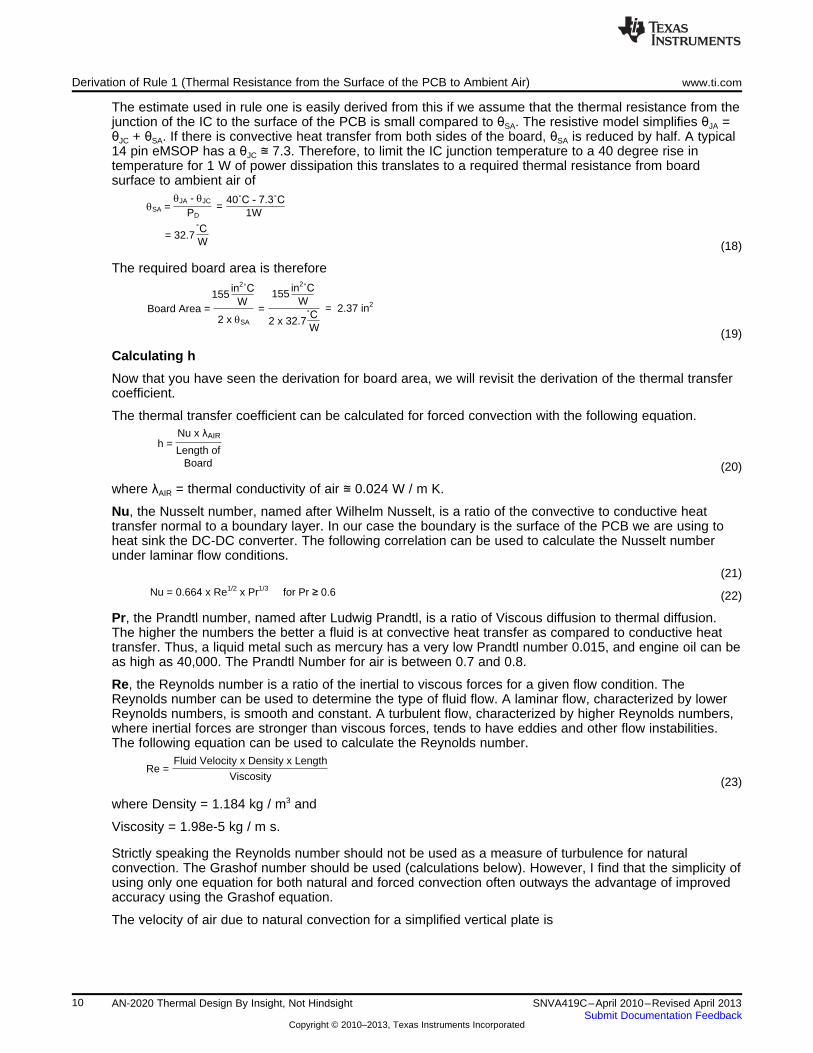
5 Derivation of Rule 1 (Thermal Resistance from the Surface of the PCB to AmbientAir)
Heat transfer from the board to the ambient air is primarily by convection and radiation. A widely publishedfigure for the heat transfer coefficient from the surface of the PCB (h) to air is 10 W / m2K. We will use thisas a starting point and look at the derivation of the heat transfer coefficient later.
To turn h into the thermal resistance from the board surface to the ambient air θSA, we take the inverseand then convert from square meters to square inches and finally divide by the surface area.
(17)
9SNVA419C–April 2010–Revised April 2013 AN-2020 Thermal Design By Insight, Not HindsightSubmit Documentation Feedback
Copyright © 2010–2013, Texas Instruments Incorporated
Re =Viscosity
Fluid Velocity x Density x Length
Nu = 0.664 x Re1/2 x Pr1/3 for Pr 8 0.6
h =Length of
Board
Nu x èAIR
=Board Area =2 x TSA
155 in2YC
W
2 x 32.7 YC
W
= 2.37 in2155
Win2YC
TSA =
= 32.7
TJA - TJC 40YC - 7.3YC
PD=
1W
YC
W
Derivation of Rule 1 (Thermal Resistance from the Surface of the PCB to Ambient Air) www.ti.com
The estimate used in rule one is easily derived from this if we assume that the thermal resistance from thejunction of the IC to the surface of the PCB is small compared to θSA. The resistive model simplifies θJA =θJC + θSA. If there is convective heat transfer from both sides of the board, θSA is reduced by half. A typical14 pin eMSOP has a θJC ≊ 7.3. Therefore, to limit the IC junction temperature to a 40 degree rise intemperature for 1 W of power dissipation this translates to a required thermal resistance from boardsurface to ambient air of
(18)
The required board area is therefore
(19)
Calculating h
Now that you have seen the derivation for board area, we will revisit the derivation of the thermal transfercoefficient.
The thermal transfer coefficient can be calculated for forced convection with the following equation.
(20)
where λAIR = thermal conductivity of air ≊ 0.024 W / m K.
Nu, the Nusselt number, named after Wilhelm Nusselt, is a ratio of the convective to conductive heattransfer normal to a boundary layer. In our case the boundary is the surface of the PCB we are using toheat sink the DC-DC converter. The following correlation can be used to calculate the Nusselt numberunder laminar flow conditions.
(21)
(22)
Pr, the Prandtl number, named after Ludwig Prandtl, is a ratio of Viscous diffusion to thermal diffusion.The higher the numbers the better a fluid is at convective heat transfer as compared to conductive heattransfer. Thus, a liquid metal such as mercury has a very low Prandtl number 0.015, and engine oil can beas high as 40,000. The Prandtl Number for air is between 0.7 and 0.8.
Re, the Reynolds number is a ratio of the inertial to viscous forces for a given flow condition. TheReynolds number can be used to determine the type of fluid flow. A laminar flow, characterized by lowerReynolds numbers, is smooth and constant. A turbulent flow, characterized by higher Reynolds numbers,where inertial forces are stronger than viscous forces, tends to have eddies and other flow instabilities.The following equation can be used to calculate the Reynolds number.
(23)
where Density = 1.184 kg / m3 and
Viscosity = 1.98e-5 kg / m s.
Strictly speaking the Reynolds number should not be used as a measure of turbulence for naturalconvection. The Grashof number should be used (calculations below). However, I find that the simplicity ofusing only one equation for both natural and forced convection often outways the advantage of improvedaccuracy using the Grashof equation.
The velocity of air due to natural convection for a simplified vertical plate is
10 AN-2020 Thermal Design By Insight, Not Hindsight SNVA419C–April 2010–Revised April 2013Submit Documentation Feedback
Copyright © 2010–2013, Texas Instruments Incorporated
h =Length
Nu x thermal conductivity
=0.0254 m
14.39 x 0.024 W
m K
+ hRAD
+ 0.78W
m2 K
hRAD =e x ð x [TBOARD
4 - TA4]
x [(338 K)4 ± (298 K)4] Wm2 K40.9 x 5.67 x 10-8
TBOARD
338 K=
Nu = 0.54 x (Gr x Pr)1/4 + 0.15 x (Gr x Pr)1/3
= 0.54 x (8.77 x104 x 0.7)1/4 + 0.15 x (8.77 x104 x 0.7)1/3
Gr =TA x Kinematic Viscosity2
g x [TBOARD4 - TA
4] x Length3
=298 K x (15.68 x 10-6
9.8 x [(338 K)4 ± (298 L)4] x (0.0254 m)3ms2
m2
s2)2
VNC =TBOARD - TA
]1/2
TA0.65 x [g x Length x
338K - 298K ]1/2
298K= 0.65 x [9.8
s2m x 0.0254m x
www.ti.com References
(24)
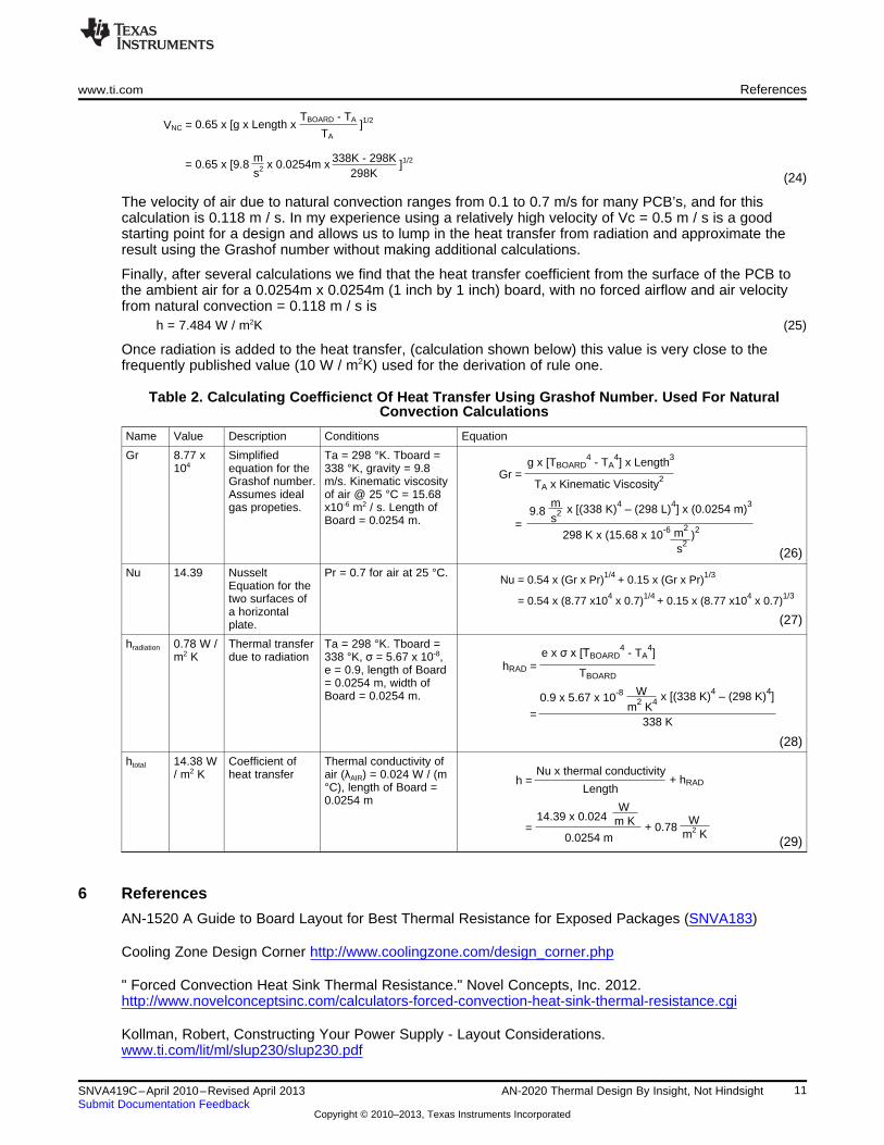
The velocity of air due to natural convection ranges from 0.1 to 0.7 m/s for many PCB’s, and for thiscalculation is 0.118 m / s. In my experience using a relatively high velocity of Vc = 0.5 m / s is a goodstarting point for a design and allows us to lump in the heat transfer from radiation and approximate theresult using the Grashof number without making additional calculations.
Finally, after several calculations we find that the heat transfer coefficient from the surface of the PCB tothe ambient air for a 0.0254m x 0.0254m (1 inch by 1 inch) board, with no forced airflow and air velocityfrom natural convection = 0.118 m / s is
h = 7.484 W / m2K (25)
Once radiation is added to the heat transfer, (calculation shown below) this value is very close to thefrequently published value (10 W / m2K) used for the derivation of rule one.
Table 2. Calculating Coefficienct Of Heat Transfer Using Grashof Number. Used For NaturalConvection Calculations
Name Value Description Conditions Equation
Gr 8.77 x Simplified Ta = 298 °K. Tboard =104 equation for the 338 °K, gravity = 9.8
Grashof number. m/s. Kinematic viscosityAssumes ideal of air @ 25 °C = 15.68gas propeties. x10-6 m2 / s. Length of
Board = 0.0254 m.
(26)
Nu 14.39 Nusselt Pr = 0.7 for air at 25 °C.Equation for thetwo surfaces ofa horizontal
(27)plate.
hradiation 0.78 W / Thermal transfer Ta = 298 °K. Tboard =m2 K due to radiation 338 °K, σ = 5.67 x 10⁻⁸,
e = 0.9, length of Board= 0.0254 m, width ofBoard = 0.0254 m.
(28)
htotal 14.38 W Coefficient of Thermal conductivity of/ m2 K heat transfer air (λAIR) = 0.024 W / (m
°C), length of Board =0.0254 m
(29)
6 References
AN-1520 A Guide to Board Layout for Best Thermal Resistance for Exposed Packages (SNVA183)
Cooling Zone Design Corner http://www.coolingzone.com/design_corner.php
" Forced Convection Heat Sink Thermal Resistance." Novel Concepts, Inc. 2012.http://www.novelconceptsinc.com/calculators-forced-convection-heat-sink-thermal-resistance.cgi
Kollman, Robert, Constructing Your Power Supply - Layout Considerations.www.ti.com/lit/ml/slup230/slup230.pdf
11SNVA419C–April 2010–Revised April 2013 AN-2020 Thermal Design By Insight, Not HindsightSubmit Documentation Feedback
Copyright © 2010–2013, Texas Instruments Incorporated
References www.ti.com
LMZ1x/EXT Thermal Resistance Estimate (SNVU041)
Mathis, Miles. "The STEFAN-BOLTZMANN LAW a simplified derivation." The General Science Journalhttp://www.wbabin.net/mathis/mathis64.pdf
12 AN-2020 Thermal Design By Insight, Not Hindsight SNVA419C–April 2010–Revised April 2013Submit Documentation Feedback
Copyright © 2010–2013, Texas Instruments Incorporated

IMPORTANT NOTICE
Texas Instruments Incorporated and its subsidiaries (TI) reserve the right to make corrections, enhancements, improvements and otherchanges to its semiconductor products and services per JESD46, latest issue, and to discontinue any product or service per JESD48, latestissue. Buyers should obtain the latest relevant information before placing orders and should verify that such information is current andcomplete. All semiconductor products (also referred to herein as “components”) are sold subject to TI’s terms and conditions of salesupplied at the time of order acknowledgment.
TI warrants performance of its components to the specifications applicable at the time of sale, in accordance with the warranty in TI’s termsand conditions of sale of semiconductor products. Testing and other quality control techniques are used to the extent TI deems necessaryto support this warranty. Except where mandated by applicable law, testing of all parameters of each component is not necessarilyperformed.
TI assumes no liability for applications assistance or the design of Buyers’ products. Buyers are responsible for their products andapplications using TI components. To minimize the risks associated with Buyers’ products and applications, Buyers should provideadequate design and operating safeguards.
TI does not warrant or represent that any license, either express or implied, is granted under any patent right, copyright, mask work right, orother intellectual property right relating to any combination, machine, or process in which TI components or services are used. Informationpublished by TI regarding third-party products or services does not constitute a license to use such products or services or a warranty orendorsement thereof. Use of such information may require a license from a third party under the patents or other intellectual property of thethird party, or a license from TI under the patents or other intellectual property of TI.
Reproduction of significant portions of TI information in TI data books or data sheets is permissible only if reproduction is without alterationand is accompanied by all associated warranties, conditions, limitations, and notices. TI is not responsible or liable for such altereddocumentation. Information of third parties may be subject to additional restrictions.
Resale of TI components or services with statements different from or beyond the parameters stated by TI for that component or servicevoids all express and any implied warranties for the associated TI component or service and is an unfair and deceptive business practice.TI is not responsible or liable for any such statements.
Buyer acknowledges and agrees that it is solely responsible for compliance with all legal, regulatory and safety-related requirementsconcerning its products, and any use of TI components in its applications, notwithstanding any applications-related information or supportthat may be provided by TI. Buyer represents and agrees that it has all the necessary expertise to create and implement safeguards whichanticipate dangerous consequences of failures, monitor failures and their consequences, lessen the likelihood of failures that might causeharm and take appropriate remedial actions. Buyer will fully indemnify TI and its representatives against any damages arising out of the useof any TI components in safety-critical applications.
In some cases, TI components may be promoted specifically to facilitate safety-related applications. With such components, TI’s goal is tohelp enable customers to design and create their own end-product solutions that meet applicable functional safety standards andrequirements. Nonetheless, such components are subject to these terms.
No TI components are authorized for use in FDA Class III (or similar life-critical medical equipment) unless authorized officers of the partieshave executed a special agreement specifically governing such use.
Only those TI components which TI has specifically designated as military grade or “enhanced plastic” are designed and intended for use inmilitary/aerospace applications or environments. Buyer acknowledges and agrees that any military or aerospace use of TI componentswhich have not been so designated is solely at the Buyer's risk, and that Buyer is solely responsible for compliance with all legal andregulatory requirements in connection with such use.
TI has specifically designated certain components as meeting ISO/TS16949 requirements, mainly for automotive use. In any case of use ofnon-designated products, TI will not be responsible for any failure to meet ISO/TS16949.
Products Applications
Audio www.ti.com/audio Automotive and Transportation www.ti.com/automotive
Amplifiers amplifier.ti.com Communications and Telecom www.ti.com/communications
Data Converters dataconverter.ti.com Computers and Peripherals www.ti.com/computers
DLP® Products www.dlp.com Consumer Electronics www.ti.com/consumer-apps
DSP dsp.ti.com Energy and Lighting www.ti.com/energy
Clocks and Timers www.ti.com/clocks Industrial www.ti.com/industrial
Interface interface.ti.com Medical www.ti.com/medical
Logic logic.ti.com Security www.ti.com/security
Power Mgmt power.ti.com Space, Avionics and Defense www.ti.com/space-avionics-defense
Microcontrollers microcontroller.ti.com Video and Imaging www.ti.com/video
RFID www.ti-rfid.com
OMAP Applications Processors www.ti.com/omap TI E2E Community e2e.ti.com
Wireless Connectivity www.ti.com/wirelessconnectivity
Mailing Address: Texas Instruments, Post Office Box 655303, Dallas, Texas 75265Copyright © 2013, Texas Instruments Incorporated