Embed Size (px)
Citation preview

Application ReportSNOA518A–March 2008–Revised March 2008
AN-1810 LMX9830 Design Checklist.....................................................................................................................................................
ABSTRACT
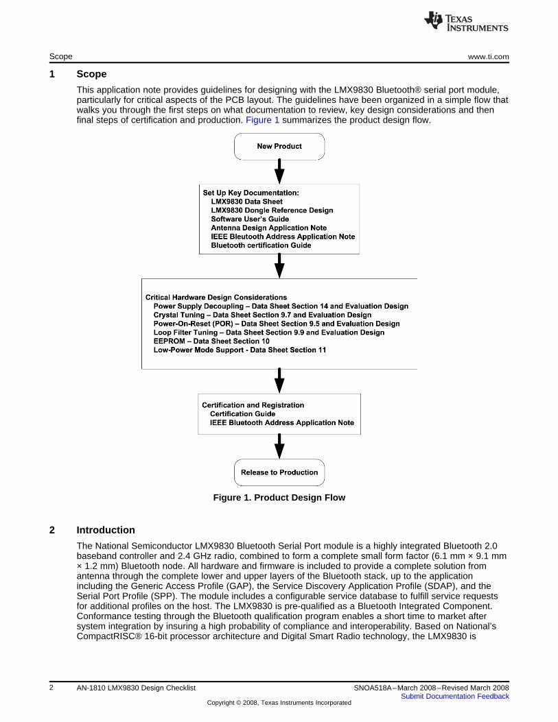
This application note provides guidelines for designing with the LMX9830 Bluetooth® serial port module,particularly for critical aspects of the PCB layout. The guidelines have been organized in a simple flow thatwalks you through the first steps on what documentation to review, key design considerations and thenfinal steps of certification and production. Figure 1 summarizes the product design flow.
Contents1 Scope ......................................................................................................................... 22 Introduction .................................................................................................................. 23 Product Design Flow ....................................................................................................... 3
3.1 DOCUMENTATION ................................................................................................ 33.2 KEY DESIGN CONSIDERATIONS .............................................................................. 33.3 CERTIFICATION AND REGISTRATION ....................................................................... 3
4 Design Flow Details ......................................................................................................... 34.1 DOCUMENTATION STRUCTURE .............................................................................. 34.2 PCB DESIGN ....................................................................................................... 4
5 Certification and Production ............................................................................................... 65.1 EXPECTED RESULTS ............................................................................................ 65.2 FIRST PROTOTYPE CHECKLIST .............................................................................. 95.3 MOST COMMON DESIGN ERRORS ........................................................................... 95.4 PRODUCT CERTIFICATION ..................................................................................... 9
6 References ................................................................................................................. 10
List of Figures
1 Product Design Flow ....................................................................................................... 2
2 Example Schematic with Critical Areas Indicated ...................................................................... 4
3 Example PCB Layout with Critical Components Indicated ............................................................ 5
4 Example Ground Layer Design with Critical Features Indicated...................................................... 5
5 Deviation Due to Modulation .............................................................................................. 7
6 Eye Diagram................................................................................................................. 7
7 BER vs. Input Power Level (dBm) ........................................................................................ 8
8 Transmit Spectrum.......................................................................................................... 8
List of Tables
1 Critical Areas ................................................................................................................ 6
All trademarks are the property of their respective owners.
1SNOA518A–March 2008–Revised March 2008 AN-1810 LMX9830 Design ChecklistSubmit Documentation Feedback
Copyright © 2008, Texas Instruments Incorporated
Scope www.ti.com
1 Scope
This application note provides guidelines for designing with the LMX9830 Bluetooth® serial port module,particularly for critical aspects of the PCB layout. The guidelines have been organized in a simple flow thatwalks you through the first steps on what documentation to review, key design considerations and thenfinal steps of certification and production. Figure 1 summarizes the product design flow.
Figure 1. Product Design Flow
2 Introduction
The National Semiconductor LMX9830 Bluetooth Serial Port module is a highly integrated Bluetooth 2.0baseband controller and 2.4 GHz radio, combined to form a complete small form factor (6.1 mm × 9.1 mm× 1.2 mm) Bluetooth node. All hardware and firmware is included to provide a complete solution fromantenna through the complete lower and upper layers of the Bluetooth stack, up to the applicationincluding the Generic Access Profile (GAP), the Service Discovery Application Profile (SDAP), and theSerial Port Profile (SPP). The module includes a configurable service database to fulfill service requestsfor additional profiles on the host. The LMX9830 is pre-qualified as a Bluetooth Integrated Component.Conformance testing through the Bluetooth qualification program enables a short time to market aftersystem integration by insuring a high probability of compliance and interoperability. Based on National’sCompactRISC® 16-bit processor architecture and Digital Smart Radio technology, the LMX9830 is
2 AN-1810 LMX9830 Design Checklist SNOA518A–March 2008–Revised March 2008Submit Documentation Feedback
Copyright © 2008, Texas Instruments Incorporated

www.ti.com Product Design Flow
optimized to handle the data and link management processing requirements of a Bluetooth node. Thefirmware supplied in the on-chip ROM offers a complete Bluetooth (v2.0) stack including profiles andcommand interface. This firmware features point-to-point and point-to-multipoint link management andsupports data rates up to the theoretical maximum over RFCOMM of 704 kbps (Best in Class in theindustry). The internal memory supports up to 7 active Bluetooth data links and one active SCO link.
3 Product Design Flow
3.1 DOCUMENTATION• LMX9830 Data Sheet [1]
• LMX9830 Dongle Reference Design and Layout [2] [7]
• Software User’s Guide [3]
• Bluetooth Antenna Design Application Note [4]
• IEEE Bluetooth Device Address Documentation [5]
• Bluetooth Certification Guide [6]
3.2 KEY DESIGN CONSIDERATIONS• Power Supply Decoupling—refer to the data sheet [1] and reference design schematics and layout [2].
• Antenna—refer to the antenna design application note [4].
• Crystal—refer to the data sheet [1].
• Power-On Reset (POR)—refer to the data sheet [1].
• Loop Filter Tuning - refer to the datasheet [1] and LMX9830 Dongle reference design documents [7].
• EEPROM—refer to the data sheet for the NVS contents [1].
• Low-Power Mode—refer to the data sheet [1].
3.3 CERTIFICATION AND REGISTRATION• Bluetooth Certification Guide [6]
• Bluetooth Device Address Management—refer to the IEEE Bluetooth device address application note[5]
4 Design Flow Details
4.1 DOCUMENTATION STRUCTURE
4.1.1 Design Documents• LMX9830 Data Sheet—contains key performance details regarding the device, pin description,
functional details, programming details, package information, and application information.
• LMX9830 Dongle Reference Design and Layout—a design example with circuit schematics and PCBlayout. It is strongly recommended to use the reference design documentation to complete the layoutfor the LMX9830. Reference design files (Gerber) and Bill of Materials are all provided on thereference design CD. These files can easily be imported into schematic capture/layout designpackages such as Orcad and PADS.
• Software User’s Guide—reference for implementing the LMX9830 module into a system. A gettingstarted session gives a very detailed entry point for starting software development. The AdvancedUsage section describes all features and configuration parameters in detail and gives examples forusing the LMX9830 as an active Bluetooth node. Finally all commands and events are listed andexplained in the command section.
• Bluetooth Antenna Design Application Note—contains detailed information about the design of theBluetooth antenna including matching to the module and a list of antenna component suppliers.
3SNOA518A–March 2008–Revised March 2008 AN-1810 LMX9830 Design ChecklistSubmit Documentation Feedback
Copyright © 2008, Texas Instruments Incorporated

Design Flow Details www.ti.com
4.1.2 Certification and Production Documents• Bluetooth Certification Guide—best practices and details for obtaining Bluetooth qualification and also
regulatory certification such as FCC or CE that is required for all designs before entering theproduction stage.
• IEEE Bluetooth Device Address Documentation—information on obtaining a unique Bluetooth deviceaddress from the IEEE, including the procedure and costs.
4.2 PCB DESIGN
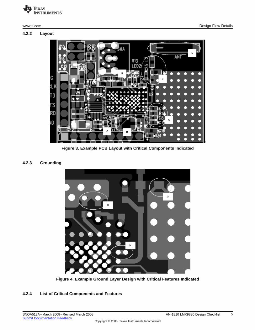
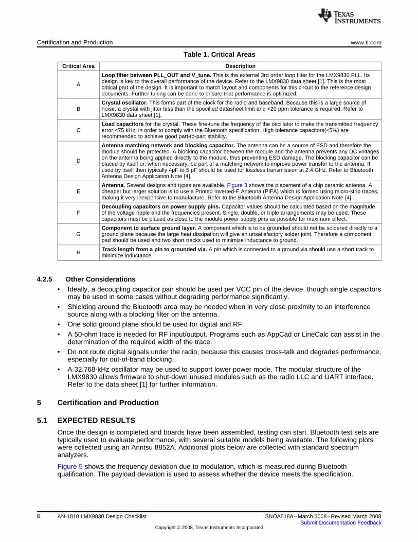
The following section discusses the layout requirements for the PCB. Figure 2, Figure 3 and Figure 4 aretaken from the LMX9830 UART buffer Dongle reference design. Capital letters mark critical areas whichare discussed further in Section 4.2.4.
4.2.1 Schematic
Figure 2. Example Schematic with Critical Areas Indicated
4 AN-1810 LMX9830 Design Checklist SNOA518A–March 2008–Revised March 2008Submit Documentation Feedback
Copyright © 2008, Texas Instruments Incorporated
www.ti.com Design Flow Details
4.2.2 Layout
Figure 3. Example PCB Layout with Critical Components Indicated
4.2.3 Grounding
Figure 4. Example Ground Layer Design with Critical Features Indicated
4.2.4 List of Critical Components and Features
5SNOA518A–March 2008–Revised March 2008 AN-1810 LMX9830 Design ChecklistSubmit Documentation Feedback
Copyright © 2008, Texas Instruments Incorporated
Certification and Production www.ti.com
Table 1. Critical Areas
Critical Area Description
Loop filter between PLL_OUT and V_tune. This is the external 3rd order loop filter for the LMX9830 PLL. Itsdesign is key to the overall performance of the device. Refer to the LMX9830 data sheet [1]. This is the mostA critical part of the design. It is important to match layout and components for this circuit to the reference designdocuments. Further tuning can be done to ensure that performance is optimized.
Crystal oscillator. This forms part of the clock for the radio and baseband. Because this is a large source ofB noise, a crystal with jitter less than the specified datasheet limit and <20 ppm tolerance is required. Refer to
LMX9830 data sheet [1].
Load capacitors for the crystal. These fine-tune the frequency of the oscillator to make the transmitted frequencyC error <75 kHz, in order to comply with the Bluetooth specification. High tolerance capacitors(<5%) are
recommended to achieve good part-to-part stability.
Antenna matching network and blocking capacitor. The antenna can be a source of ESD and therefore themodule should be protected. A blocking capacitor between the module and the antenna prevents any DC voltageson the antenna being applied directly to the module, thus preventing ESD damage. The blocking capacitor can beD placed by itself or, when necessary, be part of a matching network to improve power transfer to the antenna. Ifused by itself then typically 4pF to 5 pF should be used for lossless transmission at 2.4 GHz. Refer to BluetoothAntenna Design Application Note [4].
Antenna. Several designs and types are available. Figure 3 shows the placement of a chip ceramic antenna. AE cheaper but larger solution is to use a Printed Inverted-F Antenna (PIFA) which is formed using micro-strip traces,
making it very inexpensive to manufacture. Refer to the Bluetooth Antenna Design Application Note [4].
Decoupling capacitors on power supply pins. Capacitor values should be calculated based on the magnitudeF of the voltage ripple and the frequencies present. Single, double, or triple arrangements may be used. These
capacitors must be placed as close to the module power supply pins as possible for maximum effect.
Component to surface ground layer. A component which is to be grounded should not be soldered directly to aG ground plane because the large heat dissipation will give an unsatisfactory solder joint. Therefore a component
pad should be used and two short tracks used to minimize inductance to ground.
Track length from a pin to grounded via. A pin which is connected to a ground via should use a short track toH minimize inductance.
4.2.5 Other Considerations• Ideally, a decoupling capacitor pair should be used per VCC pin of the device, though single capacitors
may be used in some cases without degrading performance significantly.
• Shielding around the Bluetooth area may be needed when in very close proximity to an interferencesource along with a blocking filter on the antenna.
• One solid ground plane should be used for digital and RF.
• A 50-ohm trace is needed for RF input/output. Programs such as AppCad or LineCalc can assist in thedetermination of the required width of the trace.
• Do not route digital signals under the radio, because this causes cross-talk and degrades performance,especially for out-of-band blocking.
• A 32.768-kHz oscillator may be used to support lower power mode. The modular structure of theLMX9830 allows firmware to shut-down unused modules such as the radio LLC and UART interface.Refer to the data sheet [1] for further information.
5 Certification and Production
5.1 EXPECTED RESULTS
Once the design is completed and boards have been assembled, testing can start. Bluetooth test sets aretypically used to evaluate performance, with several suitable models being available. The following plotswere collected using an Anritsu 8852A. Additional plots below are collected with standard spectrumanalyzers.
Figure 5 shows the frequency deviation due to modulation, which is measured during Bluetoothqualification. The payload deviation is used to assess whether the device meets the specification.
6 AN-1810 LMX9830 Design Checklist SNOA518A–March 2008–Revised March 2008Submit Documentation Feedback
Copyright © 2008, Texas Instruments Incorporated

www.ti.com Certification and Production
Figure 5. Deviation Due to Modulation
Figure 6 is an eye diagram, which shows three features of the transmitter:
• The resolution or clarity of the diagram itself is proportional to the amount of noise present within thetransmit spectrum. A noisy spectrum will have a much smaller eye opening.
• The center crossing point shows the frequency error.
• The opening of the eye is the payload deviation.
Figure 6. Eye Diagram
The Frame Error Rate (FER) and the Bit Error Rate (BER) are a measure of receiver quality. Figure 7shows typical BER performance. The Sensitivity Specification states the at -70dBm the BER should bebetter than 0.1%. The BER and FER should both be close to 0% when signal level is >-70 dBm. The BERshould only exceed 0.1% at <-80 dBm.
7SNOA518A–March 2008–Revised March 2008 AN-1810 LMX9830 Design ChecklistSubmit Documentation Feedback
Copyright © 2008, Texas Instruments Incorporated

Certification and Production www.ti.com
Figure 7. BER vs. Input Power Level (dBm)
The modulation spectrum in Figure 8 shows the 20 dBc Bandwidth is less than 1000 kHz, as required bythe Bluetooth specification. The limit prevents interference with neighboring channels.
Figure 8. Transmit Spectrum
8 AN-1810 LMX9830 Design Checklist SNOA518A–March 2008–Revised March 2008Submit Documentation Feedback
Copyright © 2008, Texas Instruments Incorporated

www.ti.com Certification and Production
5.2 FIRST PROTOTYPE CHECKLIST
If the expected results cannot be obtained from the first prototypes, the following points should bechecked:
• Test at least 3 to 5 boards to make sure the failure is consistent with the design and not board-dependent.
• Inspect the boards under a PCB microscope, checking for dry or short-circuited joints.
• Check power supply, digital I/O, and radio are within the data sheet specified range.
• X-ray can be used to inspect the quality of soldering under the module. Too little solder will form drygaps, excess will lead to overspill and shorts between pins.
• Check that the crystal is turning on during power-up using a high-impedance probe. Check that thefrequency is ±240 Hz of the desired frequency. The crystal can be tuned using internal registers or theload capacitors.
• Check the power-supply noise ripple on the VCC pins is within 15 mVp-p. A large capacitor on theoutput of the LDO will smooth low-frequency ripple.
• Loop filter tweaks may be required if performance measurements are generally poor. Refer to the datasheet for details.
• Antenna matching may be required to improve radiated sensitivity and power, therefore range. Refer tothe Bluetooth antenna design application note.
• A front-end filter (either LC or ceramic) may be required for additional blocking margin. Refer to theBluetooth antenna design application note.
5.3 MOST COMMON DESIGN ERRORS
These are some of the more common errors when designing with the LMX9830.
5.3.1 Non-Compact Design
When there is more than enough space on the PCB which must be of a certain shape and size to conformto the application, some designers tend to spread the external components over a larger area than isrequired. This is a mistake. Though there may be space available, the external components such as loopfilter, decoupling capacitors, crystal, etc. must be placed as close to the LMX9830 as possible, otherwisedegraded performance due to unnecessary line parasitics will result.
5.3.2 Poor Grounding
Not using enough ground vias or ground lines that are too thin and long is a common error. Long tracksare inductive, and high-frequency currents do not get down to the ground plane fast enough, resulting incross-coupling and spurious emissions.
5.3.3 No Antenna-Matching Network or External Filter
Though a purchased antenna may work well on its test PCB, it may not have the same performance onthe final design PCB. A common mistake is to forget the matching network or room for filtering that willadd versatility to the design and allow for antenna tuning and better blocking performance.
5.3.4 Badly Tuned Crystal
Like the antenna, the crystal oscillator’s frequency is subject to pull when placed on the final applicationPCB due to parasitic stray capacitance. Not tuning the crystal on the final design is therefore a commoncause of initial poor performance.
5.4 PRODUCT CERTIFICATION
Refer to the Bluetooth certification guide which describes the steps and preparation needed to get fullregulatory and Bluetooth certification for a new product, including lists of required tests and detailedprocedures. The key steps required to achieve certification, as described in the certification guide, are:
1. Become an Adopter or Member of the Bluetooth SIG.
9SNOA518A–March 2008–Revised March 2008 AN-1810 LMX9830 Design ChecklistSubmit Documentation Feedback
Copyright © 2008, Texas Instruments Incorporated

References www.ti.com
2. Review the design guide, data sheet and complete documentation package for a selected NationalSemiconductor product.
3. Design the schematic and component layout. The critical grounding and decoupling required for theradio must be studied in detail.
4. Generate the schematic and layout Gerber files for the final application.
5. Compare schematics and layout files to details in datasheet, reference designs and application notes.
6. Implement the design changes as agreed in the review.
7. Production of first prototypes (between 10 and 20 units).
8. At least five units must be tested fully over the temperature range.
9. Any failure or marginal pass of the specification must be corrected by component change or layoutmodification.
10. Test the DUTs again to verify that all parameters are within specification.
11. Prepare three “golden units” for the BQTF, two with antenna connectors and one with an originalantenna.
12. Select the BQTF and prepare documentation for DUTs.
13. Submit the documentation and DUTs to the BQTF for regulatory and Bluetooth qualification tests.
14. Product will be listed on the official Bluetooth web page as Bluetooth compliant when all test caseshave passed.
15. Release product to manufacturing.
6 References
Ref. Title Type File Name
1 LMX9830 Bluetooth Serial Port Module Data Sheet LMX9830DS.pdf
2 LMX9830 Dongle Hardware User Guide User Guide LMX9830DONGLE Hardware User Guide.pdf
3 LMX9830 Software Users Guide Users Guide LMX9830_SW_UG.pdf
4 Bluetooth Antenna Design Application Note Bluetooth Antenna Design.pdf
5 Bluetooth Device Address for the LMX9830 Application Note BD_ADDR AN.pdf
6 Bluetooth Certification Guide Application Note BT Cert Guide Complete.pdf
LMX9830Dongle without UART Buffer.DSN
LMX9830DONGLE PADS file.pcb7 LMX9830 Dongle Reference Design Design FilesLMX9830DONGLE_BOM_without UARTBuffer.xls
NOTE: Dongle without UART buffer is a more accurate form factor design. UART buffer is used for5V interface to PC for testing only. UART buffers is not needed for 3V designs.
10 AN-1810 LMX9830 Design Checklist SNOA518A–March 2008–Revised March 2008Submit Documentation Feedback
Copyright © 2008, Texas Instruments Incorporated

IMPORTANT NOTICE
Texas Instruments Incorporated and its subsidiaries (TI) reserve the right to make corrections, enhancements, improvements and otherchanges to its semiconductor products and services per JESD46, latest issue, and to discontinue any product or service per JESD48, latestissue. Buyers should obtain the latest relevant information before placing orders and should verify that such information is current andcomplete. All semiconductor products (also referred to herein as “components”) are sold subject to TI’s terms and conditions of salesupplied at the time of order acknowledgment.
TI warrants performance of its components to the specifications applicable at the time of sale, in accordance with the warranty in TI’s termsand conditions of sale of semiconductor products. Testing and other quality control techniques are used to the extent TI deems necessaryto support this warranty. Except where mandated by applicable law, testing of all parameters of each component is not necessarilyperformed.
TI assumes no liability for applications assistance or the design of Buyers’ products. Buyers are responsible for their products andapplications using TI components. To minimize the risks associated with Buyers’ products and applications, Buyers should provideadequate design and operating safeguards.
TI does not warrant or represent that any license, either express or implied, is granted under any patent right, copyright, mask work right, orother intellectual property right relating to any combination, machine, or process in which TI components or services are used. Informationpublished by TI regarding third-party products or services does not constitute a license to use such products or services or a warranty orendorsement thereof. Use of such information may require a license from a third party under the patents or other intellectual property of thethird party, or a license from TI under the patents or other intellectual property of TI.
Reproduction of significant portions of TI information in TI data books or data sheets is permissible only if reproduction is without alterationand is accompanied by all associated warranties, conditions, limitations, and notices. TI is not responsible or liable for such altereddocumentation. Information of third parties may be subject to additional restrictions.
Resale of TI components or services with statements different from or beyond the parameters stated by TI for that component or servicevoids all express and any implied warranties for the associated TI component or service and is an unfair and deceptive business practice.TI is not responsible or liable for any such statements.
Buyer acknowledges and agrees that it is solely responsible for compliance with all legal, regulatory and safety-related requirementsconcerning its products, and any use of TI components in its applications, notwithstanding any applications-related information or supportthat may be provided by TI. Buyer represents and agrees that it has all the necessary expertise to create and implement safeguards whichanticipate dangerous consequences of failures, monitor failures and their consequences, lessen the likelihood of failures that might causeharm and take appropriate remedial actions. Buyer will fully indemnify TI and its representatives against any damages arising out of the useof any TI components in safety-critical applications.
In some cases, TI components may be promoted specifically to facilitate safety-related applications. With such components, TI’s goal is tohelp enable customers to design and create their own end-product solutions that meet applicable functional safety standards andrequirements. Nonetheless, such components are subject to these terms.
No TI components are authorized for use in FDA Class III (or similar life-critical medical equipment) unless authorized officers of the partieshave executed a special agreement specifically governing such use.
Only those TI components which TI has specifically designated as military grade or “enhanced plastic” are designed and intended for use inmilitary/aerospace applications or environments. Buyer acknowledges and agrees that any military or aerospace use of TI componentswhich have not been so designated is solely at the Buyer's risk, and that Buyer is solely responsible for compliance with all legal andregulatory requirements in connection with such use.
TI has specifically designated certain components which meet ISO/TS16949 requirements, mainly for automotive use. Components whichhave not been so designated are neither designed nor intended for automotive use; and TI will not be responsible for any failure of suchcomponents to meet such requirements.
Products Applications
Audio www.ti.com/audio Automotive and Transportation www.ti.com/automotive
Amplifiers amplifier.ti.com Communications and Telecom www.ti.com/communications
Data Converters dataconverter.ti.com Computers and Peripherals www.ti.com/computers
DLP® Products www.dlp.com Consumer Electronics www.ti.com/consumer-apps
DSP dsp.ti.com Energy and Lighting www.ti.com/energy
Clocks and Timers www.ti.com/clocks Industrial www.ti.com/industrial
Interface interface.ti.com Medical www.ti.com/medical
Logic logic.ti.com Security www.ti.com/security
Power Mgmt power.ti.com Space, Avionics and Defense www.ti.com/space-avionics-defense
Microcontrollers microcontroller.ti.com Video and Imaging www.ti.com/video
RFID www.ti-rfid.com
OMAP Applications Processors www.ti.com/omap TI E2E Community e2e.ti.com
Wireless Connectivity www.ti.com/wirelessconnectivity
Mailing Address: Texas Instruments, Post Office Box 655303, Dallas, Texas 75265Copyright © 2012, Texas Instruments Incorporated