Embed Size (px)
Citation preview
Purpose of Communication: The purpose of a communication system is to transmit information-bearing signals or baseband signalsthrough a communication channel separating the transmitter from the receiver.
Baseband: Baseband is used to designate the band of frequencies representing the original signal as delivered by a source of information.
Communication Channel: The communication channel may be a transmission line (as in telephony and telegraphy), an optical fiber (as in optical communications) or merely free space in which the information-bearing signal is radiated as an electromagnetic wave (as in radio and television broadcasting).
The proper utilization of the communication channel requires a shift of the range of baseband frequencies into other frequency ranges suitable for transmission, and a corresponding shift back to the original frequency range after reception.
A shift of the range of frequencies in a signal is accomplished by using modulation.
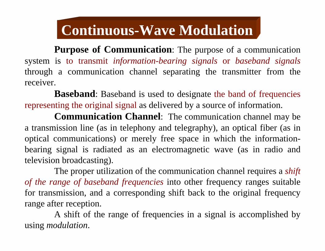
Continuous-Wave Modulation
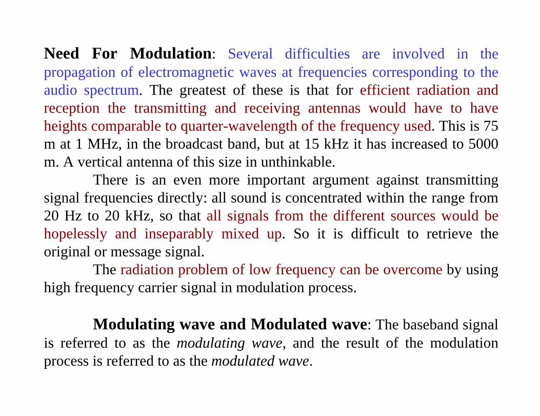
Need For Modulation: Several difficulties are involved in the propagation of electromagnetic waves at frequencies corresponding to the audio spectrum. The greatest of these is that for efficient radiation and reception the transmitting and receiving antennas would have to have heights comparable to quarter-wavelength of the frequency used. This is 75 m at 1 MHz, in the broadcast band, but at 15 kHz it has increased to 5000 m. A vertical antenna of this size in unthinkable.
There is an even more important argument against transmitting signal frequencies directly: all sound is concentrated within the range from 20 Hz to 20 kHz, so that all signals from the different sources would be hopelessly and inseparably mixed up. So it is difficult to retrieve the original or message signal.
The radiation problem of low frequency can be overcome by using high frequency carrier signal in modulation process.
Modulating wave and Modulated wave: The baseband signal is referred to as the modulating wave, and the result of the modulation process is referred to as the modulated wave.
Modulation is performed at the transmission end of the communication system.
Modulation: Modulation is defined as the process by which some characteristic of a carrier is varied in accordance with a modulating wave (signal).
In the process of modulation, some characteristic of a high-frequency sine wave (the carrier) is varied in accordance with the instantaneous values of the (modulating) signal.
A common form of the carrier is a sinusoidal wave.
Demodulation: The receiving end of the system, we usually require the original baseband to be restored. This is accomplished by using a process known as demodulation, which is reverse of the modulation process.
Since a common form of the carrier is a sinusoidal wave, in which case the modulation process referred as continuous-wave modulation.
Classification of Modulation:There are two forms of the continuous-wave modulations:
(a) Amplitude modulation (AM), and(b) Angle Modulation.
There are also two forms angle modulations:(a) Phase modulation (PM) and (b) Frequency modulation (FM).
Amplitude Modulation (AM): Amplitude modulation (AM) is defined as a process in which the amplitude of the carrier wave c(t) is varied about a mean value, linearly with the baseband signal m(t).
Let, a sinusoidal carrier wave c(t) defined by
c(t)=Accos(2πfct) (3.1)
where, Ac is the carrier amplitude and fc is the carrier frequency.
Let m(t) denote the baseband signal that carries the specification of the message. Then, an amplitude modulated (AM) wave may thus be described, in its most general form, as a function of time as follows:
s(t)=Ac[1+Kam(t)]cos(2πfct) (3.2)where, Ka is a constant called the amplitude sensitivity.
The carrier amplitude Ac and the message signal measured in volts, which case the amplitude sensitivity Ka is measured in volt-1.
Amplitude Modulation
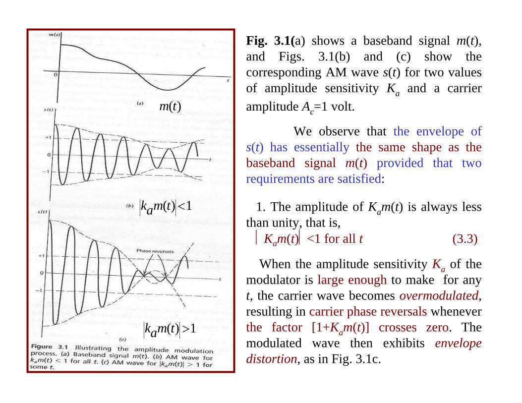
Fig. 3.1(a) shows a baseband signal m(t), and Figs. 3.1(b) and (c) show the corresponding AM wave s(t) for two values of amplitude sensitivity Ka and a carrier amplitude Ac=1 volt.
We observe that the envelope of s(t) has essentially the same shape as the baseband signal m(t) provided that two requirements are satisfied:
1)( <tmak
1)( >tmak
)(tm
1. The amplitude of Kam(t) is always less than unity, that is, Kam(t)<1 for all t (3.3)
When the amplitude sensitivity Ka of the modulator is large enough to make for any t, the carrier wave becomes overmodulated, resulting in carrier phase reversals whenever the factor [1+Kam(t)] crosses zero. The modulated wave then exhibits envelope distortion, as in Fig. 3.1c.
2. The carrier frequency fc is much greater than the highest frequency component W of the message signal m(t), that is
fc>>W (3.4)where, W is the message bandwidth.If the condition (3.4) is not satisfied, an envelope cannot be visualized
satisfactorily.
From Eq. (3.2), we find that the Fourier transform of the AM wave s(t) is given by
)]()([2)]()([2)( cffMcffMcAakcffcffcAfS ++−+++−= δδ
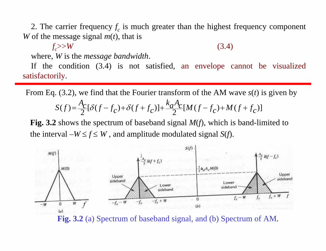
Fig. 3.2 shows the spectrum of baseband signal M(f), which is band-limited to the interval –W ≤ f ≤ W , and amplitude modulated signal S(f).
Fig. 3.2 (a) Spectrum of baseband signal, and (b) Spectrum of AM.
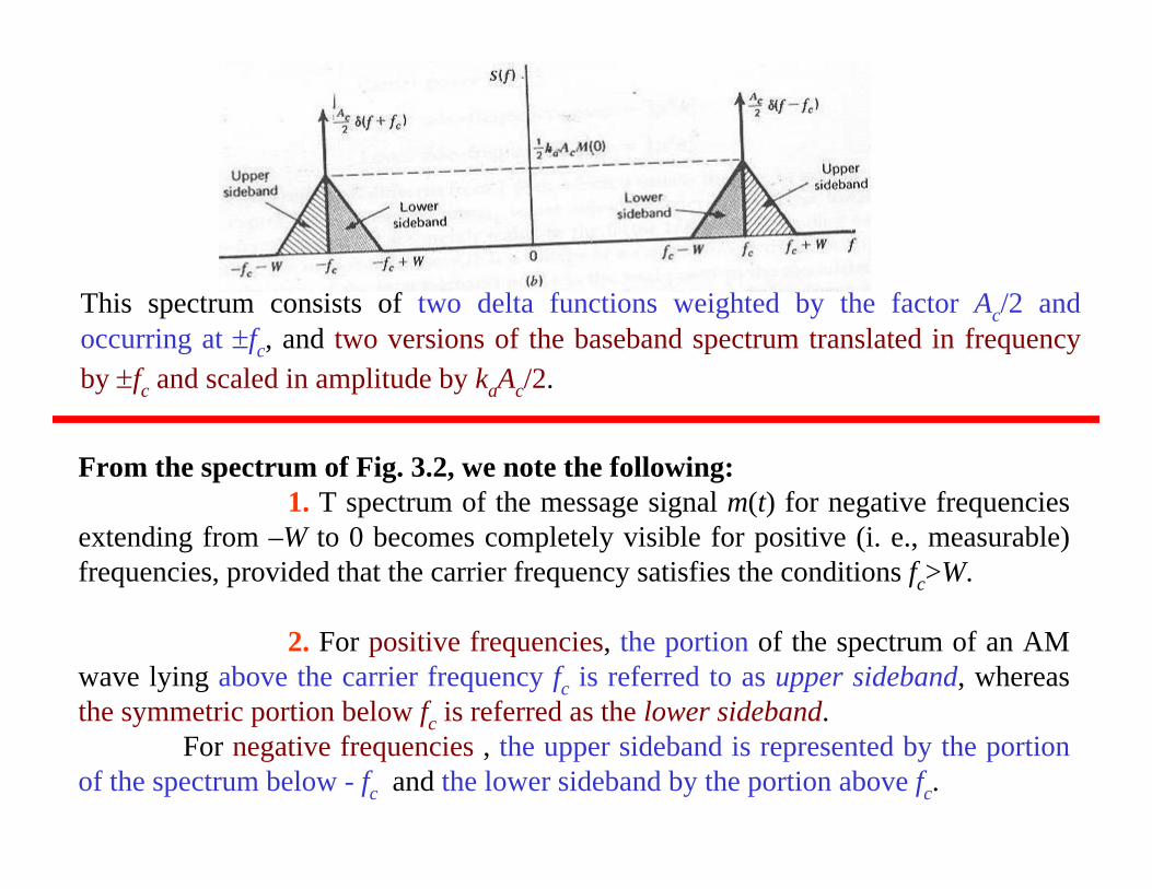
This spectrum consists of two delta functions weighted by the factor Ac/2 and occurring at ±fc, and two versions of the baseband spectrum translated in frequency by ±fc and scaled in amplitude by kaAc/2.
From the spectrum of Fig. 3.2, we note the following:1. T spectrum of the message signal m(t) for negative frequencies
extending from –W to 0 becomes completely visible for positive (i. e., measurable) frequencies, provided that the carrier frequency satisfies the conditions fc>W.
2. For positive frequencies, the portion of the spectrum of an AM wave lying above the carrier frequency fc is referred to as upper sideband, whereas the symmetric portion below fc is referred as the lower sideband.
For negative frequencies , the upper sideband is represented by the portion of the spectrum below - fc and the lower sideband by the portion above fc.
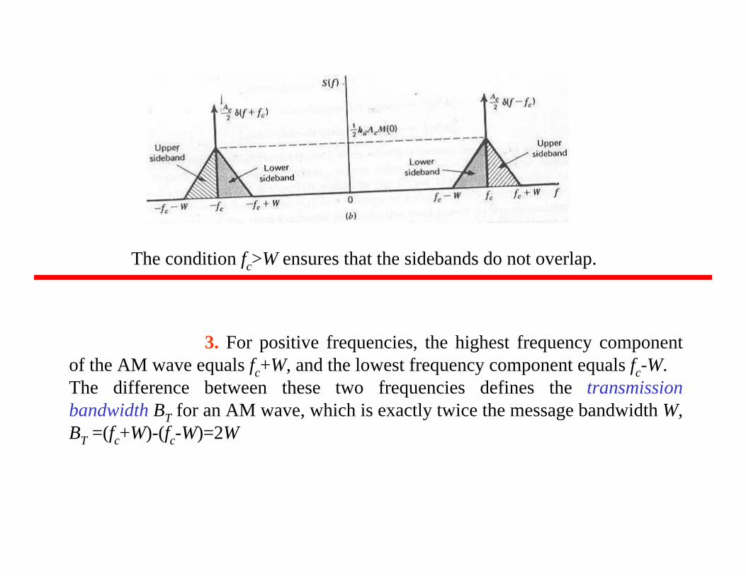
3. For positive frequencies, the highest frequency component of the AM wave equals fc+W, and the lowest frequency component equals fc-W.The difference between these two frequencies defines the transmission bandwidth BT for an AM wave, which is exactly twice the message bandwidth W,BT =(fc+W)-(fc-W)=2W
The condition fc>W ensures that the sidebands do not overlap.
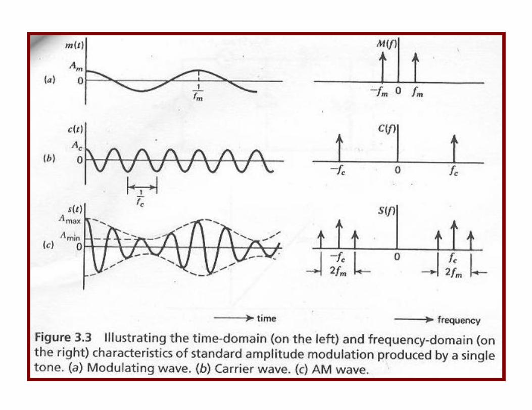
Single-Tone ModulationSingle Tone Signal: The signal which has only one frequency is called single tonesignal.
Consider a modulating wave m(t) that consists of a single tone or frequency component and a carrier wave c(t) can be written as follows:
m(t)=Amcos(2πfmt) c(t)=Accos(2πfct)where, Am and Ac are the amplitude of modulating wave and carrier wave, and fm
and fc are the frequency of modulating wave and carrier wave.
The corresponding AM wave is therefore given by:s(t)= Ac[1+Ka Amcos(2πfmt)]cos(2πfct)=Ac[1+µcos(2πfmt)]cos(2πfct) (3.7)Where, modulation factor, µ =Ka Am
To avoid envelope distortion due to overmodulation, the modulation factor µ must be kept below unity (i.e. µ<1).
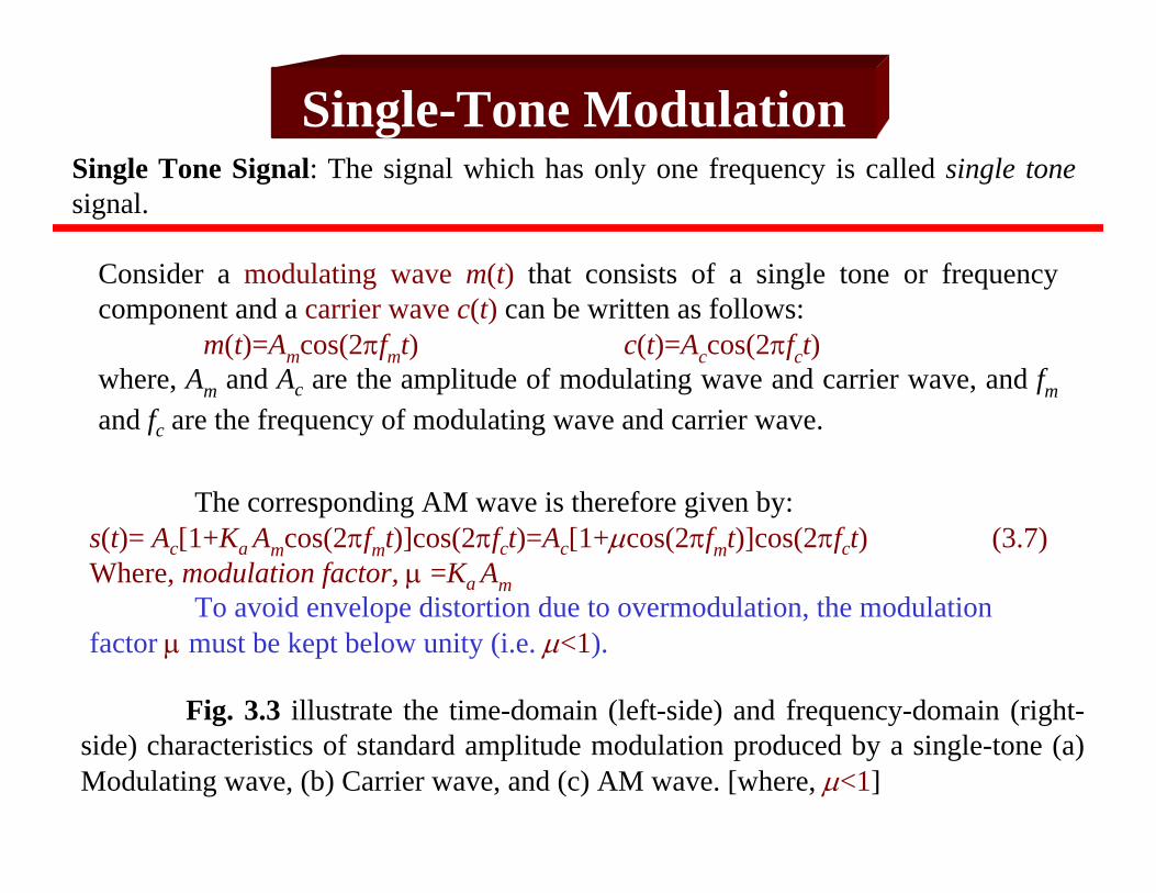
Fig. 3.3 illustrate the time-domain (left-side) and frequency-domain (right-side) characteristics of standard amplitude modulation produced by a single-tone (a) Modulating wave, (b) Carrier wave, and (c) AM wave. [where, µ<1]
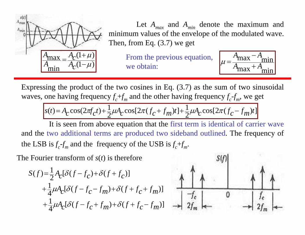
Let Amax and Amin denote the maximum and minimum values of the envelope of the modulated wave. Then, from Eq. (3.7) we get
)1()1(
minmax
µµ
−+=
cAcA
AA
minmaxminmax
AAAA
+−
=µFrom the previous equation, we obtain:
Expressing the product of the two cosines in Eq. (3.7) as the sum of two sinusoidal waves, one having frequency fc+fm and the other having frequency fc-fm, we get
])(2cos[21])(2cos[2
1)2cos()( tmfcfcAtmfcfcAtcfcAts −+++= πµπµπ
It is seen from above equation that the first term is identical of carrier waveand the two additional terms are produced two sideband outlined. The frequency of the LSB is fc-fm and the frequency of the USB is fc+fm.
)]()([41
)]()([41
)]()([21)(
mfcffmfcffcA
mfcffmfcffcA
cffcffcAfS
−+++−+
+++−−+
++−=
δδµ
δδµ
δδ
The Fourier transform of s(t) is therefore
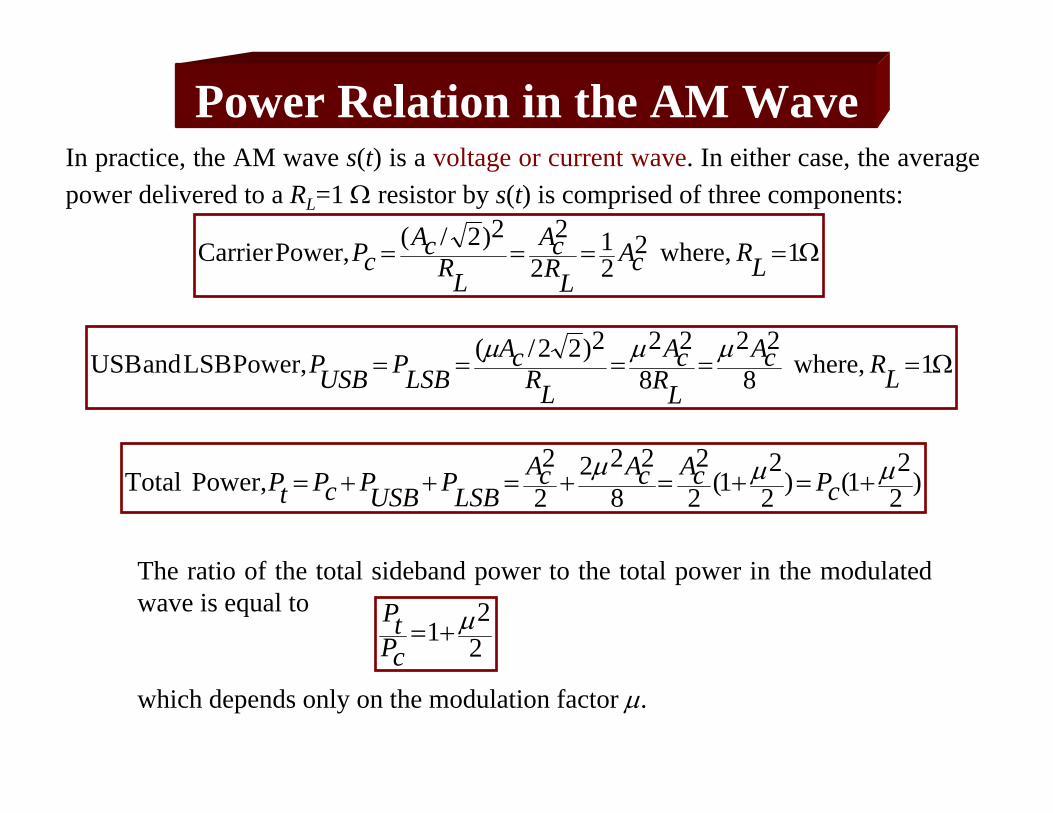
Power Relation in the AM WaveIn practice, the AM wave s(t) is a voltage or current wave. In either case, the average power delivered to a RL=1 Ω resistor by s(t) is comprised of three components:
Ω==== 1where,221
222)2/(Power,Carrier LRcALR
cA
LRcA
cP
Ω===== 1where,822
8222)22/(Power,LSBandUSB LRcA
LRcA
LRcA
LSBPUSBP µµµ
)22
1()22
1(22
8222
22
Power,Total µµµ +=+=+=++= cPcAcAcALSBPUSBPcPtP
The ratio of the total sideband power to the total power in the modulated wave is equal to
which depends only on the modulation factor µ.
22
1 µ+=cPtP
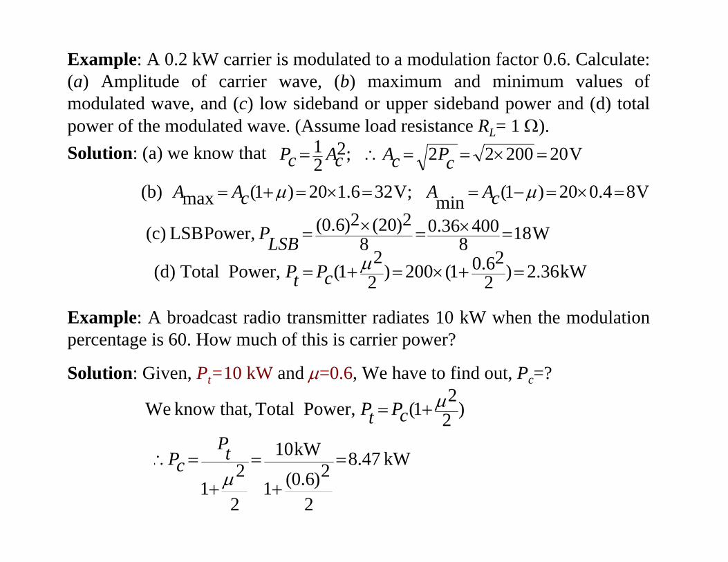
Example: A 0.2 kW carrier is modulated to a modulation factor 0.6. Calculate: (a) Amplitude of carrier wave, (b) maximum and minimum values of modulated wave, and (c) low sideband or upper sideband power and (d) total power of the modulated wave. (Assume load resistance RL= 1 Ω).Solution: (a) we know that V2020022;2
21 =×==∴= cPcAcAcP
V84.020)1(minV;326.120)1(max(b) =×=−==×=+= µµ cAAcAA
W18840036.0
82)20(2)6.0(Power,LSB (c) =×=×=LSBP
kW36.2)226.01(200)2
21(Power,Total(d) =+×=+= µ
cPtP
Example: A broadcast radio transmitter radiates 10 kW when the modulation percentage is 60. How much of this is carrier power?
)22
1(Power,Total that,know We µ+= cPtP
Solution: Given, Pt=10 kW and µ=0.6, We have to find out, Pc=?
kW47.8
2
2)6.0(1
kW10
2
21
=
+
=
+
=∴µtP
cP
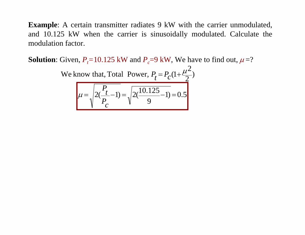
Example: A certain transmitter radiates 9 kW with the carrier unmodulated, and 10.125 kW when the carrier is sinusoidally modulated. Calculate the modulation factor.
)22
1(Power,Total that,know We µ+= cPtP
Solution: Given, Pt=10.125 kW and Pc=9 kW, We have to find out, µ=?
5.0)19125.10(2)1(2 =−=−=
cPtP
µ
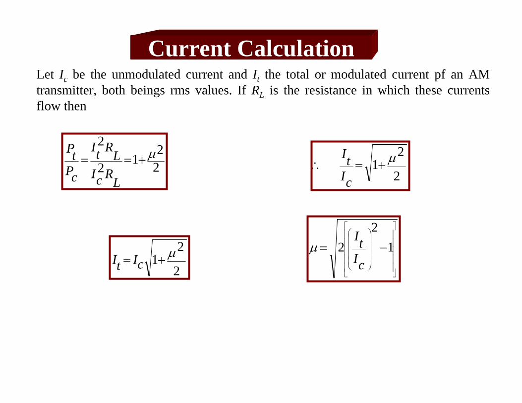
Current CalculationLet Ic be the unmodulated current and It the total or modulated current pf an AM transmitter, both beings rms values. If RL is the resistance in which these currents flow then
22
12
2µ+==
LRcILRtI
cPtP
2
21 µ+=∴
cItI
2
21 µ+= cItI ⎥
⎥⎥⎥⎥
⎦
⎤
⎢⎢⎢⎢⎢
⎣
⎡
⎟⎟⎟⎟
⎠
⎞
⎜⎜⎜⎜
⎝
⎛
−= 12
2cItIµ
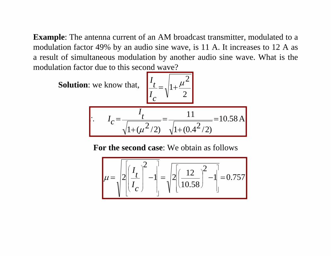
Example: The antenna current of an AM broadcast transmitter, modulated to a modulation factor 49% by an audio sine wave, is 11 A. It increases to 12 A as a result of simultaneous modulation by another audio sine wave. What is the modulation factor due to this second wave?
2
21 µ+=
cItISolution: we know that,
A58.10)2/24.0(1
11
)2/2(1=
+=
+=∴
µtIcI
757.012
58.101221
22 =−=−=
⎥⎥⎥⎥
⎦
⎤
⎢⎢⎢⎢
⎣
⎡
⎟⎟
⎠
⎞
⎜⎜
⎝
⎛
⎥⎥⎥⎥⎥
⎦
⎤
⎢⎢⎢⎢⎢
⎣
⎡
⎟⎟⎟⎟
⎠
⎞
⎜⎜⎜⎜
⎝
⎛
cItIµ
For the second case: We obtain as follows
Generation of AM waves
The AM waves can be generated by using two devices namely (a) the square-law modulator, and (b) the switching modulator.
To implement these two modulator, a nonlinear element is required. And these two devices are well-suited for low power modulation purpose.
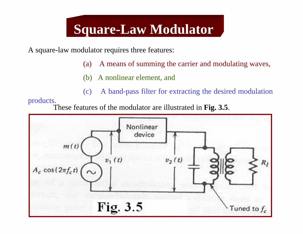
Square-Law ModulatorA square-law modulator requires three features:
(a) A means of summing the carrier and modulating waves,
(b) A nonlinear element, and
(c) A band-pass filter for extracting the desired modulation products.
These features of the modulator are illustrated in Fig. 3.5.
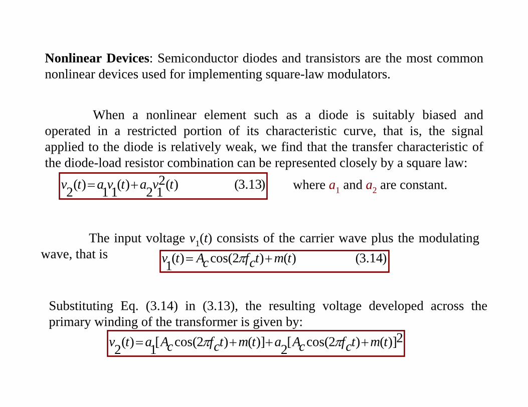
Nonlinear Devices: Semiconductor diodes and transistors are the most common nonlinear devices used for implementing square-law modulators.
where a1 and a2 are constant.
When a nonlinear element such as a diode is suitably biased and operated in a restricted portion of its characteristic curve, that is, the signal applied to the diode is relatively weak, we find that the transfer characteristic of the diode-load resistor combination can be represented closely by a square law:
)13.3()(212)(11)(2 tvatvatv +=
The input voltage v1(t) consists of the carrier wave plus the modulating wave, that is )14.3()()2cos()(1 tmtcfcAtv += π
Substituting Eq. (3.14) in (3.13), the resulting voltage developed across the primary winding of the transformer is given by:
2)]()2cos([2)]()2cos([1)(2 tmtcfcAatmtcfcAatv +++= ππ
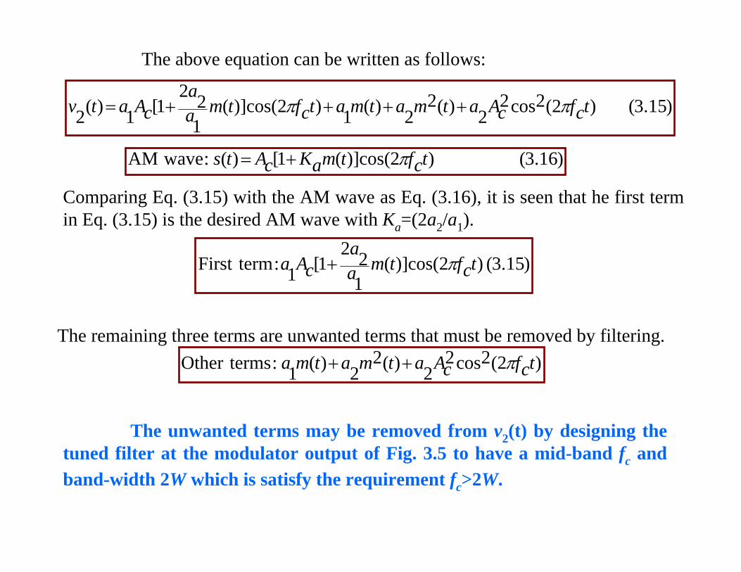
)15.3()2(2cos22)(2
2)(1)2cos()](122
1[1)(2 tcfcAatmatmatcftmaa
cAatv ππ ++++=
Comparing Eq. (3.15) with the AM wave as Eq. (3.16), it is seen that he first term in Eq. (3.15) is the desired AM wave with Ka=(2a2/a1).
)15.3()2cos()](122
1[1:termFirst tcftmaa
cAa π+
The remaining three terms are unwanted terms that must be removed by filtering. )2(2cos2
2)(22)(1:termsOther tcfcAatmatma π++
)16.3()2cos()](1[)(:waveAM tcftmaKcAts π+=
The unwanted terms may be removed from v2(t) by designing the tuned filter at the modulator output of Fig. 3.5 to have a mid-band fc and band-width 2W which is satisfy the requirement fc>2W.
The above equation can be written as follows:
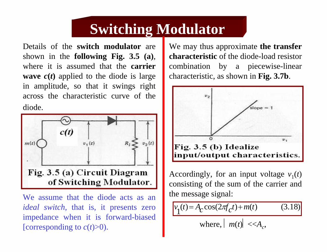
Switching ModulatorDetails of the switch modulator are shown in the following Fig. 3.5 (a), where it is assumed that the carrier wave c(t) applied to the diode is large in amplitude, so that it swings right across the characteristic curve of the diode.
We assume that the diode acts as an ideal switch, that is, it presents zero impedance when it is forward-biased [corresponding to c(t)>0).
We may thus approximate the transfer characteristic of the diode-load resistor combination by a piecewise-linear characteristic, as shown in Fig. 3.7b.
Accordingly, for an input voltage v1(t) consisting of the sum of the carrier and the message signal:
)18.3()()2cos()(1 tmtcfcAtv += π
where, m(t)<<Ac,
The Expression for the load voltage v2(t) is given by:
)19.3(0)(,00)(),(1)(2 ⎪⎩
⎪⎨
⎧
<
>=
tctctv
tv
We may express Eq. (3.19) mathematically as :)20.3()()]()2cos([)(2 tpgtmtcfcAtv += π
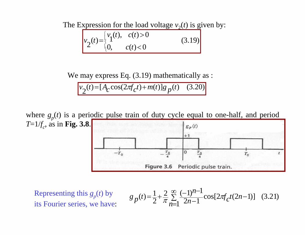
where gp(t) is a periodic pulse train of duty cycle equal to one-half, and period T=1/fc, as in Fig. 3.8.
)21.3(1
)]12(2cos[121)1(2
21)( ∑
∞
=−−
−−+=n
ntcfnn
tpg ππRepresenting this gp(t) by its Fourier series, we have:
Therefore, substituting Eq. (3.21) in (3.20), we find that the load voltage v2(t) consists of the sum of two components:
1. The components
which is the desired AM wave with amplitude sensitivity ka=4/πAc. The switching modulator is therefore made more sensitivity by reducing the carrier amplitude Ac; however, it must be maintained large enough to make the diode act like an ideal switch.
)2cos()](41[2 tcftmcA
cA ππ+
2. Unwanted components, the spectrum of which contains delta functions at 0, ±2fc, and ±4fc so on, and which occupy frequency intervals of width 2W centered at 0, ±3fc, ±5fc, and so on, where W is the message bandwidth.
The unwanted terms are removed from the load voltage v2(t) by means of a band-pass filter with mid-band frequency fc, and bandwidth 2W, provided that fc>2W.
Envelope-Detector
The process of demodulation is used to recover the original modulating wave from the incoming modulated wave; in effect, demodulation is the reverse of the modulation process.
The demodulation of an AM wave can be accomplished using various devices; here, we describe a simple and yet highlyeffective device known as the envelop-detector.
An envelop detector of the series type is shown in Fig. 3.7, which consists of a diode and a resistor-capacitor (RC) filter. The operation of this envelope detector is as follows.
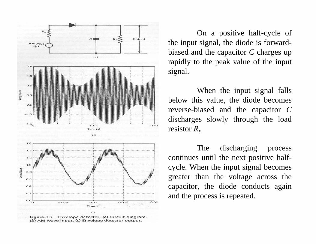
On a positive half-cycle of the input signal, the diode is forward-biased and the capacitor C charges up rapidly to the peak value of the input signal.
When the input signal falls below this value, the diode becomes reverse-biased and the capacitor Cdischarges slowly through the load resistor Rl.
The discharging process continues until the next positive half-cycle. When the input signal becomes greater than the voltage across the capacitor, the diode conducts again and the process is repeated.
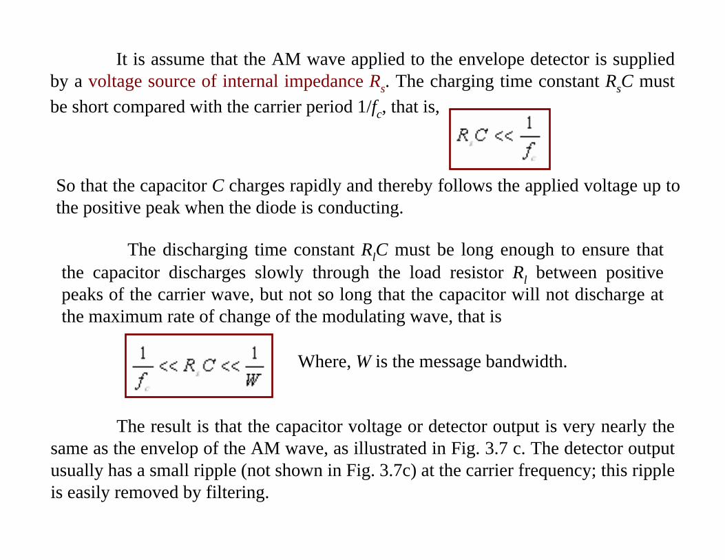
It is assume that the AM wave applied to the envelope detector is supplied by a voltage source of internal impedance Rs. The charging time constant RsC must be short compared with the carrier period 1/fc, that is,
So that the capacitor C charges rapidly and thereby follows the applied voltage up to the positive peak when the diode is conducting.
The discharging time constant RlC must be long enough to ensure that the capacitor discharges slowly through the load resistor Rl between positive peaks of the carrier wave, but not so long that the capacitor will not discharge at the maximum rate of change of the modulating wave, that is
Where, W is the message bandwidth.
The result is that the capacitor voltage or detector output is very nearly the same as the envelop of the AM wave, as illustrated in Fig. 3.7 c. The detector output usually has a small ripple (not shown in Fig. 3.7c) at the carrier frequency; this ripple is easily removed by filtering.