Embed Size (px)
Citation preview
Amplifiers with Improved Efficiency
Doherty Amplifier
Outphasing (LINC or Chireix) Amplifier
Envelope Tracking Amplifier
Envelope Elimination & Restoration Amplifier
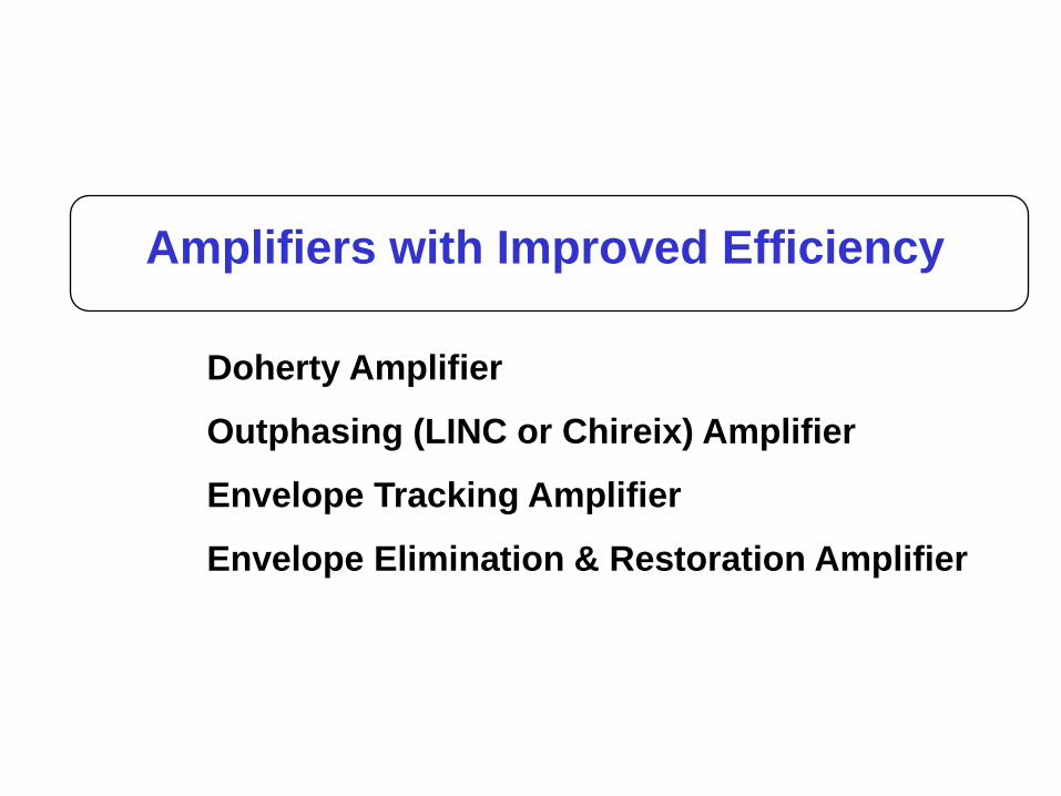
Strategies for Reduction of DC Power For
Low output Power Operation
Iout
Vout Vary bias current according to
Instantaneous power
“Dynamic biasing”
Iout
Vout V1 V2 V3
Vary bias current and voltage according to
Instantaneous power
“Envelope tracking and EER”
Iout
Vout
Vary load impedance according to
Instantaneous power
“Doherty and Chireix”
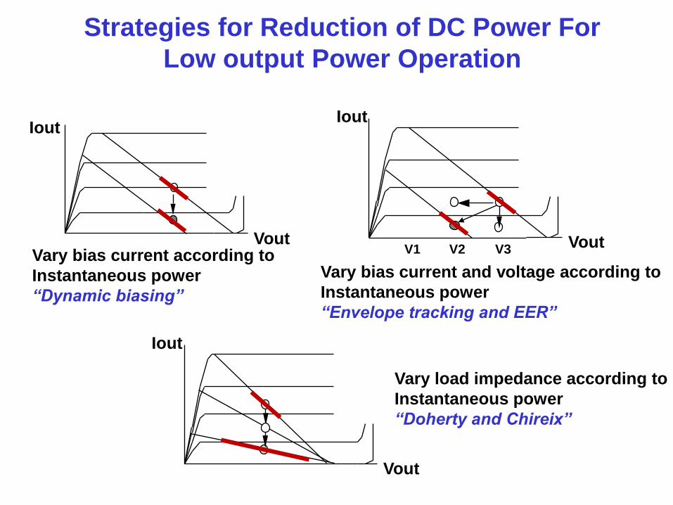
Envelope Tracking (ET) Technique
• Envelope Amplifier provides dynamic drain voltage
• Maximizes PA efficiency by keeping RF transistor
closer to saturation for all envelope amplitudes
Dynamic Drain Voltage
Time
In Envelope Tracking, PA is quasi-linear.
Input signal contains envelope and phase information.
Envelope
Amplifier
DC
Supply
RF
Signal Out
Vo
lta
ge
RF
Signal
In
RF
Amplifier
Envelope
Detector
Drain voltage tracks envelope
of RF signal
0
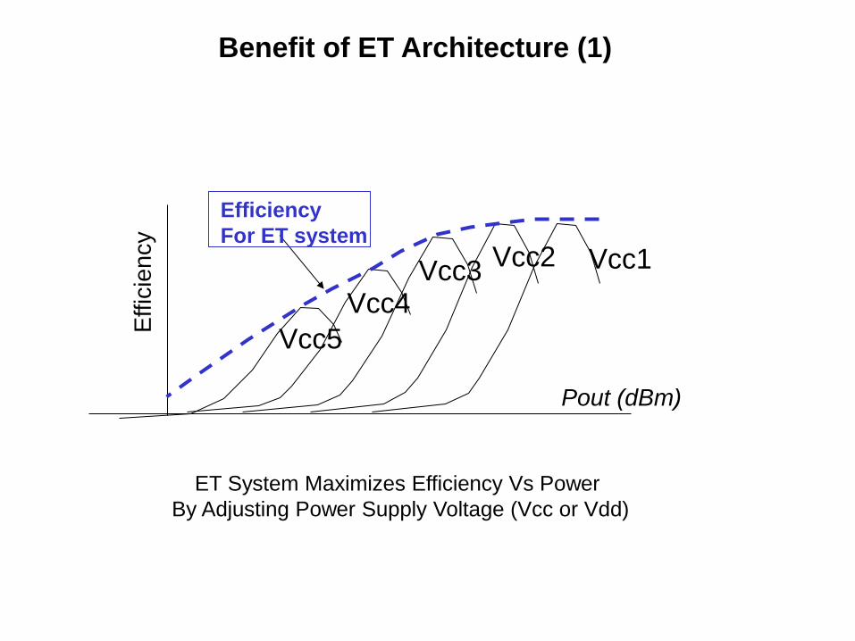
Benefit of ET Architecture (1)
Pout (dBm)
Effic
ien
cy
Vcc5
Vcc4 Vcc3
Vcc2 Vcc1
ET System Maximizes Efficiency Vs Power
By Adjusting Power Supply Voltage (Vcc or Vdd)
Efficiency
For ET system
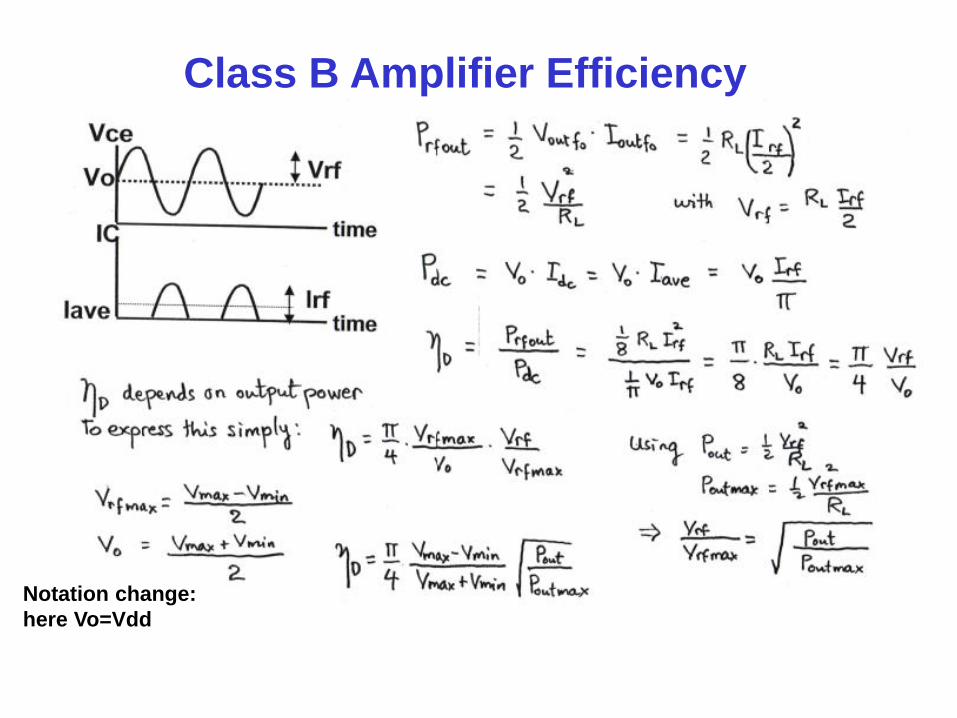
Class B Amplifier Efficiency
Notation change:
here Vo=Vdd
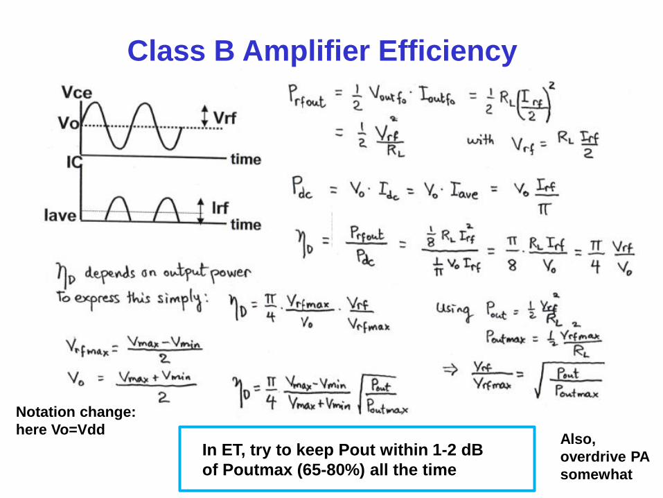
Class B Amplifier Efficiency
Notation change:
here Vo=Vdd
In ET, try to keep Pout within 1-2 dB
of Poutmax (65-80%) all the time
Also,
overdrive PA
somewhat
En
ve
lop
e &
Po
we
r S
up
ply
Vo
ltag
e (
no
rma
lize
d)
En
ve
lop
e &
Po
we
r S
up
ply
Vo
ltag
e (
no
rma
lize
d)
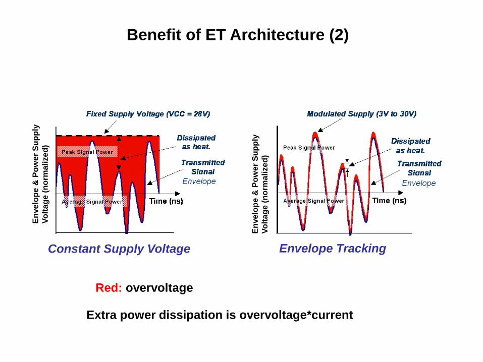
Constant Supply Voltage Envelope Tracking
Benefit of ET Architecture (2)
Extra power dissipation is overvoltage*current
Red: overvoltage
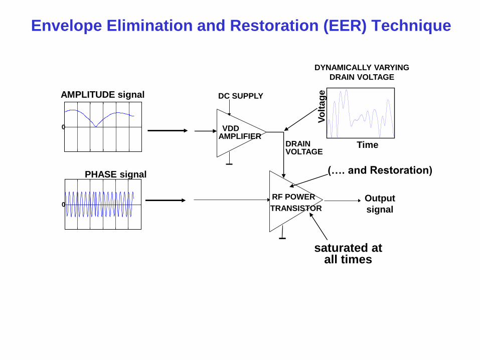
Envelope Elimination and Restoration (EER) Technique
saturated at all times
RF POWER
TRANSISTOR
VDD AMPLIFIER
DRAIN VOLTAGE
DC SUPPLY AMPLITUDE signal
0
PHASE signal
0 Output
signal
(…. and Restoration)
DYNAMICALLY VARYING
DRAIN VOLTAGE
Vo
lta
ge
Time
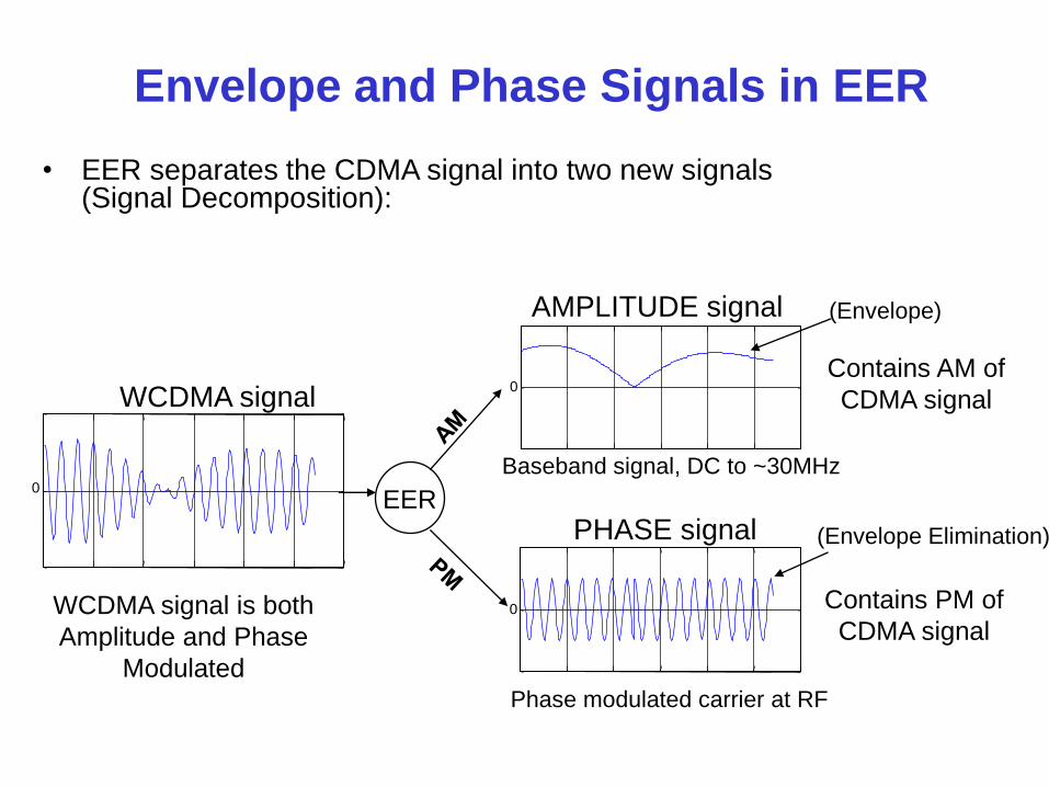
Envelope and Phase Signals in EER • EER separates the CDMA signal into two new signals (Signal Decomposition):
AMPLITUDE signal
0
PHASE signal
0
0
WCDMA signal
EER
WCDMA signal is both
Amplitude and Phase
Modulated
Contains AM of
CDMA signal
Contains PM of
CDMA signal
Baseband signal, DC to ~30MHz
Phase modulated carrier at RF
(Envelope Elimination)
(Envelope)
Earl McCune
saturated at all times
RF POWER
TRANSISTOR
VDD AMPLIFIER
DRAIN VOLTAGE
DC SUPPLY AMPLITUDE signal
0
PHASE signal
0 Output
signal
(…. and Restoration)
DYNAMICALLY VARYING
DRAIN VOLTAGE
Vo
ltag
e
Time Envelope
Amplifier
DC
Supply
RF
Signal
Out
RF
Signal
In
RF
Amplifier
Envelope
Detector
Drain voltage tracks
envelope of RF signal
0
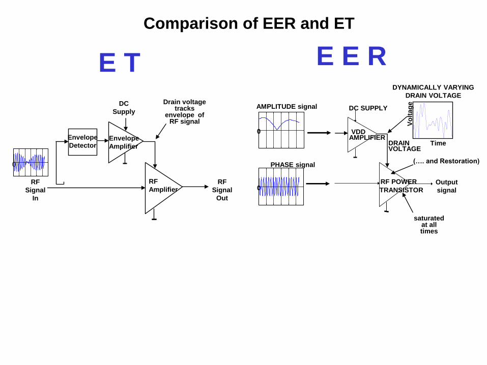
E T E E R
Comparison of EER and ET
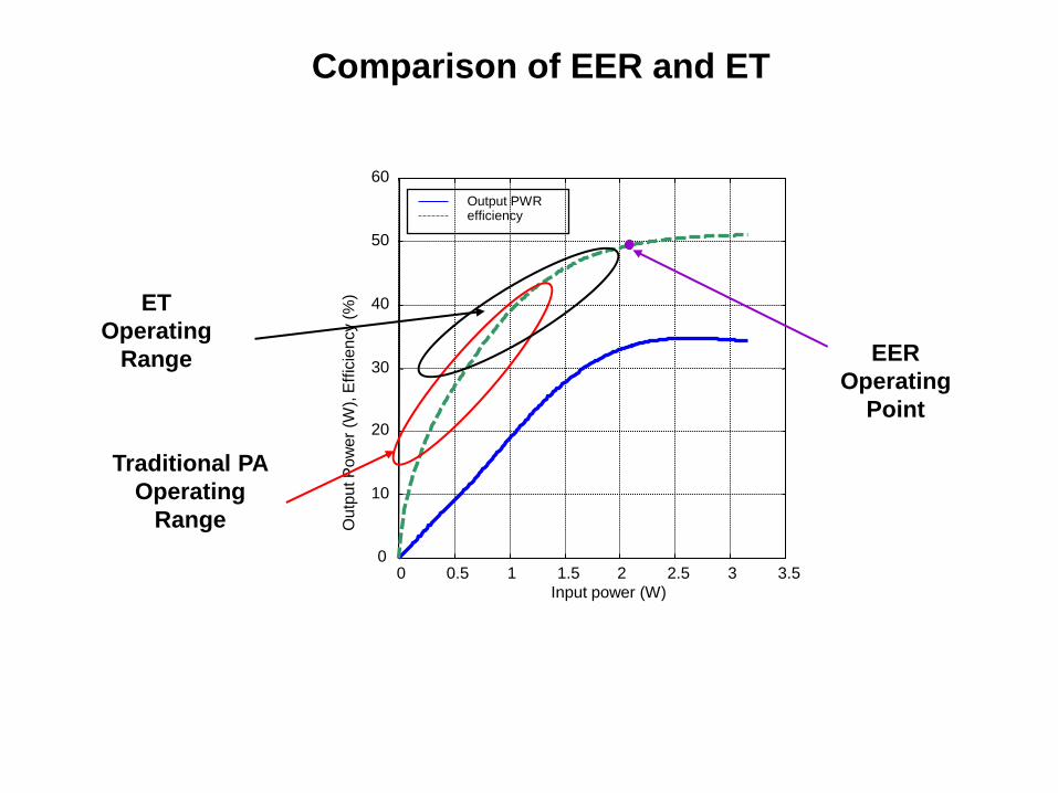
0 0.5 1 1.5 2 2.5 3 3.5 0
10
20
30
40
50
60
Input power (W)
Ou
tpu
t P
ow
er
(W),
Eff
icie
ncy (
%)
Output PWR efficiency
EER
Operating
Point
ET
Operating
Range
Traditional PA
Operating
Range
Comparison of EER and ET
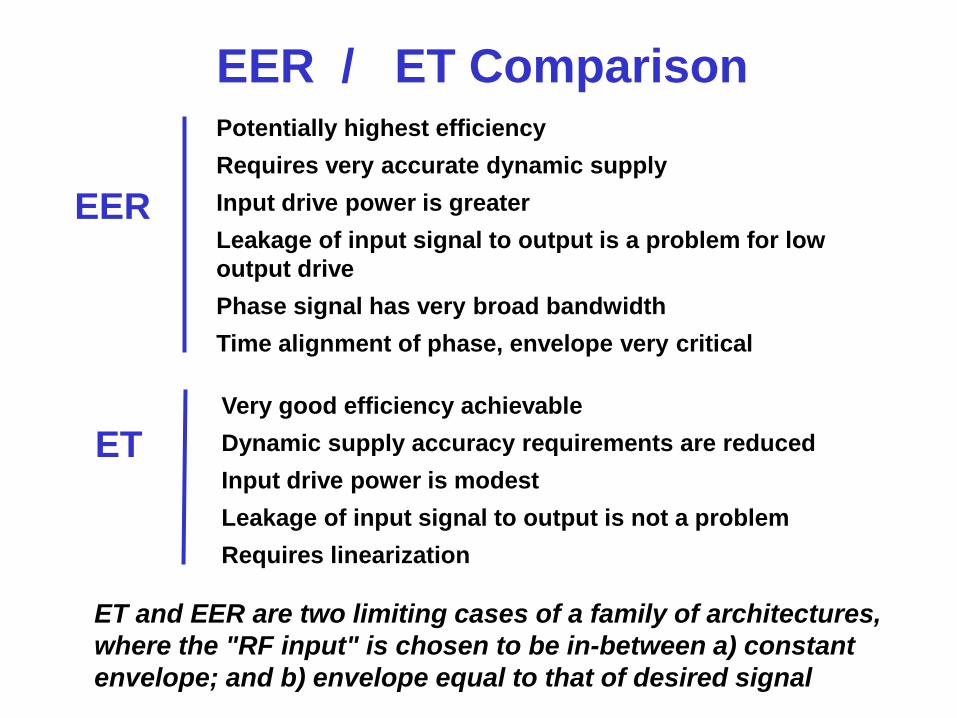
EER / ET Comparison
EER
Potentially highest efficiency
Requires very accurate dynamic supply
Input drive power is greater
Leakage of input signal to output is a problem for low
output drive
Phase signal has very broad bandwidth
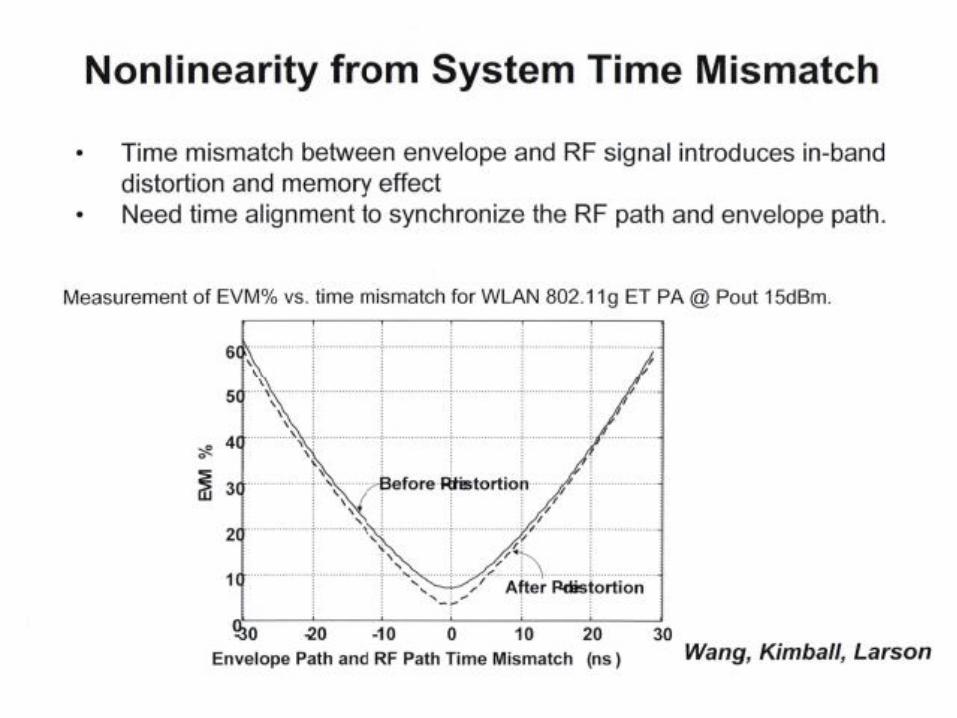
Time alignment of phase, envelope very critical
ET Very good efficiency achievable
Dynamic supply accuracy requirements are reduced
Input drive power is modest
Leakage of input signal to output is not a problem
Requires linearization
ET and EER are two limiting cases of a family of architectures,
where the "RF input" is chosen to be in-between a) constant
envelope; and b) envelope equal to that of desired signal
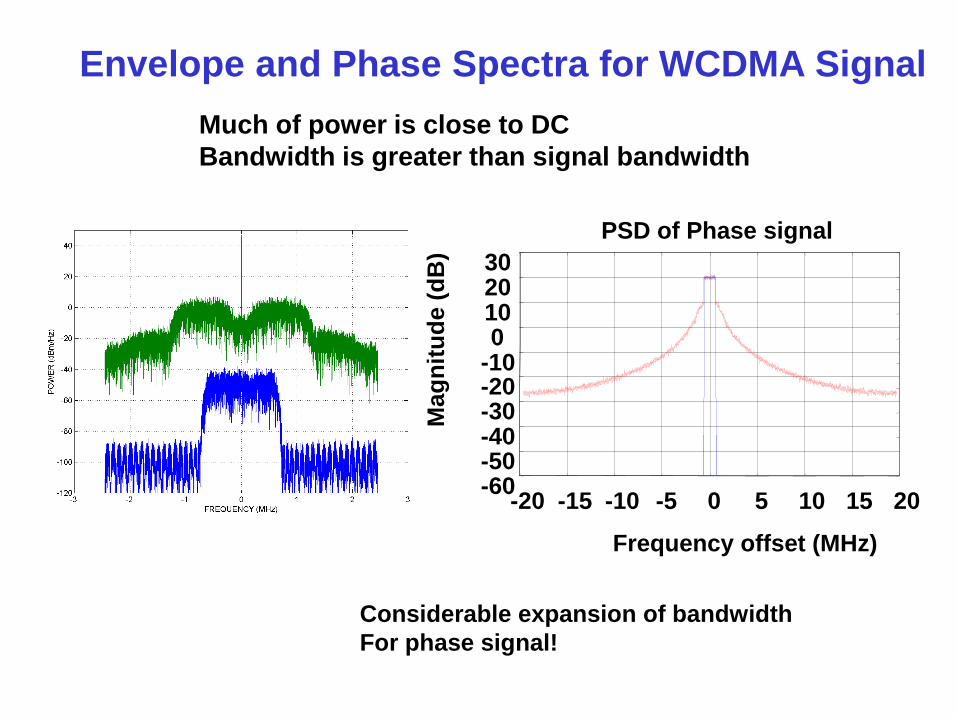
Envelope and Phase Spectra for WCDMA Signal
Much of power is close to DC
Bandwidth is greater than signal bandwidth
-20 -15 -10 -5 0 5 10 15 20 -60 -50 -40 -30 -20 -10 0 10 20 30
PSD of Phase signal
Frequency offset (MHz)
Mag
nit
ud
e (
dB
)
Considerable expansion of bandwidth
For phase signal!
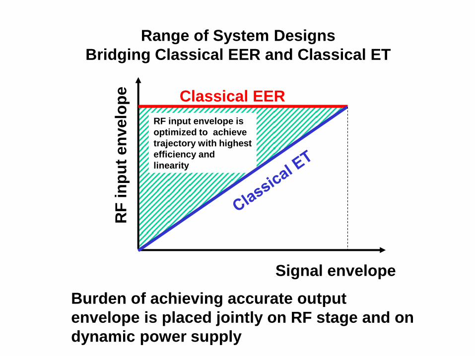
Signal envelope
RF
in
pu
t en
velo
pe
Classical EER
RF input envelope is
optimized to achieve
trajectory with highest
efficiency and
linearity
Range of System Designs
Bridging Classical EER and Classical ET
Burden of achieving accurate output
envelope is placed jointly on RF stage and on
dynamic power supply
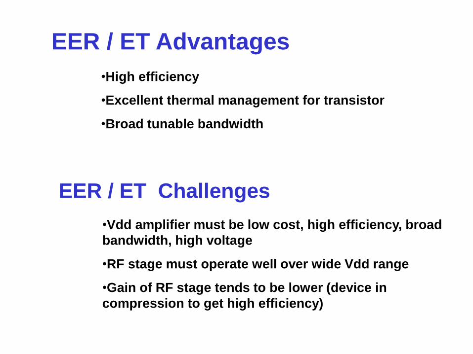
EER / ET Advantages
•High efficiency
•Excellent thermal management for transistor
•Broad tunable bandwidth
EER / ET Challenges
•Vdd amplifier must be low cost, high efficiency, broad
bandwidth, high voltage
•RF stage must operate well over wide Vdd range
•Gain of RF stage tends to be lower (device in
compression to get high efficiency)
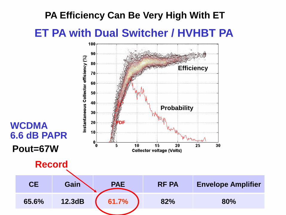
ET PA with Dual Switcher / HVHBT PA
CE Gain PAE RF PA Envelope Amplifier
65.6% 12.3dB 61.7% 82% 80%
WCDMA 6.6 dB PAPR
Record
Efficiency
Probability
Pout=67W
PA Efficiency Can Be Very High With ET
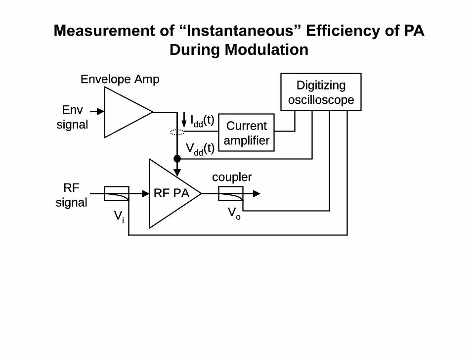
RF PA
Envelope Amp
Current
amplifier
Digitizing
oscilloscope
Vdd(t)
Idd(t)
VoVi
coupler
Env
signal
RF
signalRF PA
Envelope Amp
Current
amplifier
Digitizing
oscilloscope
Vdd(t)
Idd(t)
VoVi
coupler
Env
signal
RF
signal
Measurement of “Instantaneous” Efficiency of PA
During Modulation
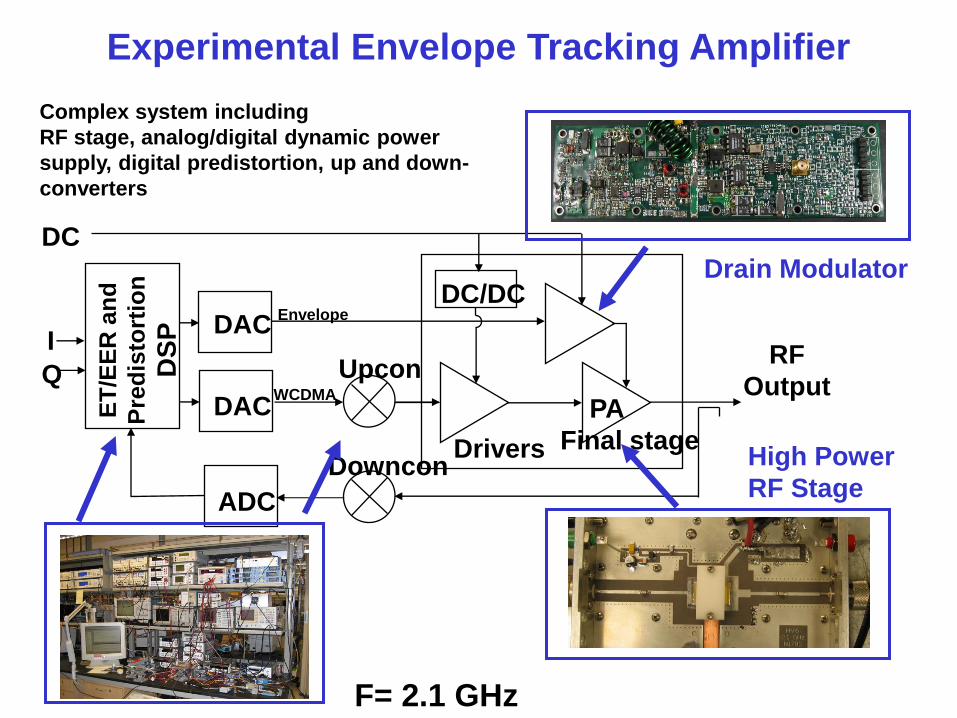
DAC
DC/DC
Drivers
DC
Upcon
DAC
Drain Modulator
WCDMA
RF
Output
Envelope
PA
Final stage
ET
/EE
R a
nd
Pre
dis
tort
ion
DS
P
I
Q
Downcon
ADC
Experimental Envelope Tracking Amplifier
High Power
RF Stage
F= 2.1 GHz
Complex system including
RF stage, analog/digital dynamic power
supply, digital predistortion, up and down-
converters
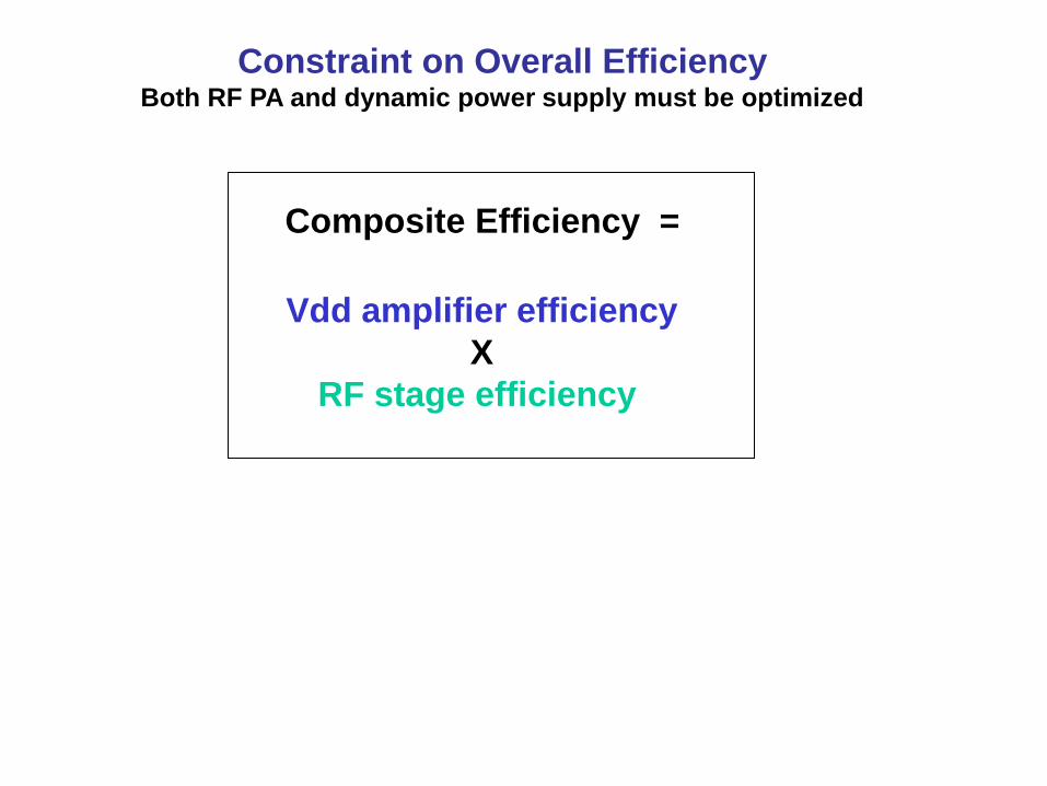
Vdd amplifier efficiency
X
RF stage efficiency
Composite Efficiency =
Constraint on Overall Efficiency Both RF PA and dynamic power supply must be optimized
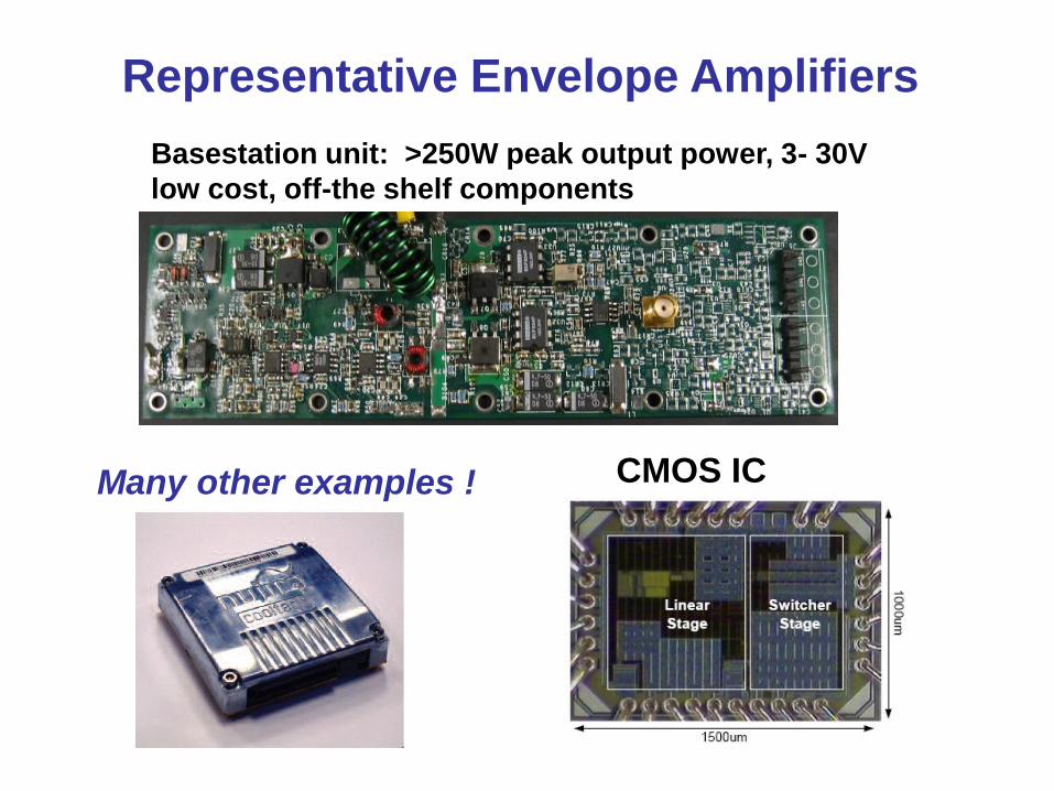
Representative Envelope Amplifiers
Basestation unit: >250W peak output power, 3- 30V
low cost, off-the shelf components
Many other examples ! CMOS IC
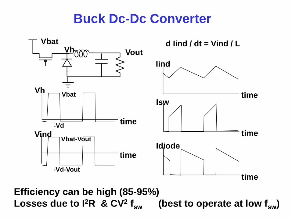
Buck Dc-Dc Converter
Vbat
Vout Vh
time
Vh Vbat
-Vd
time
Vind Vbat-Vout
-Vd-Vout
time
Iind
time
Isw
time
Idiode
d Iind / dt = Vind / L
Efficiency can be high (85-95%)
Losses due to I2R & CV2 fsw (best to operate at low fsw)
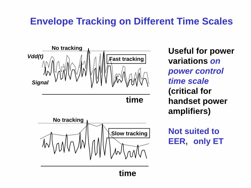
Envelope Tracking on Different Time Scales
time
time
No tracking
Fast tracking
No tracking
Slow tracking
Signal
Vdd(t) Useful for power
variations on
power control
time scale
(critical for
handset power
amplifiers)
Not suited to
EER, only ET
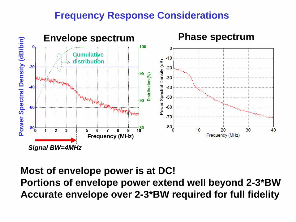
Frequency Response Considerations
Phase spectrum
Most of envelope power is at DC!
Portions of envelope power extend well beyond 2-3*BW
Accurate envelope over 2-3*BW required for full fidelity
Envelope spectrum
Po
wer
Sp
ectr
al
Den
sit
y (
dB
/bin
)
Frequency (MHz)
Signal BW=4MHz
Cumulative
distribution
Envelope
Signal
Current
Sense
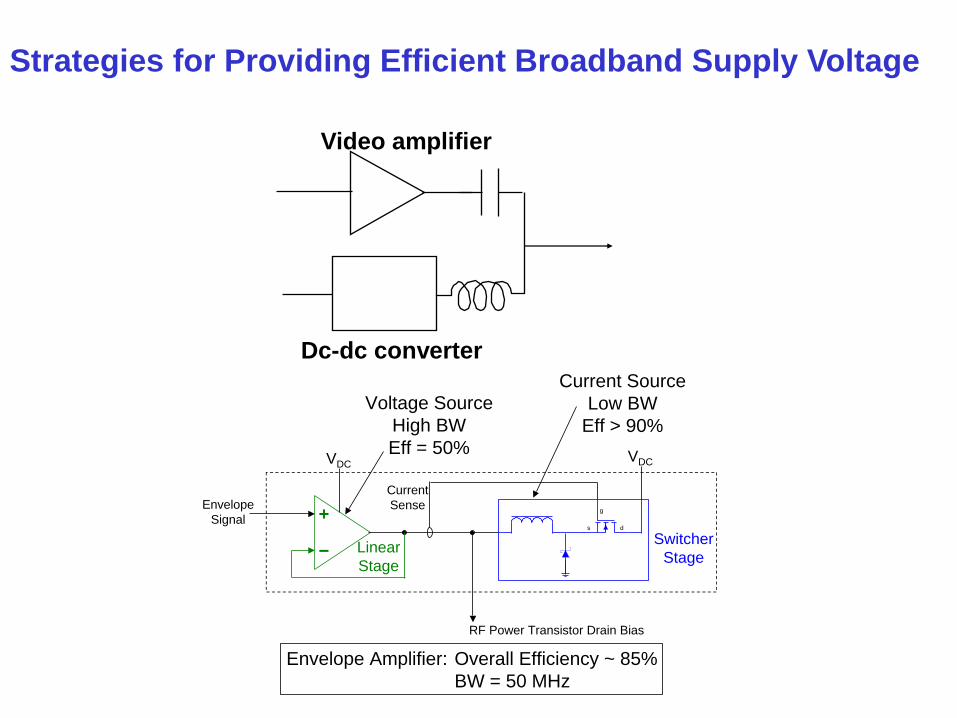
RF Power Transistor Drain Bias
Linear
Stage
g
s d
VDC
Switcher
Stage
Voltage Source
High BW
Eff = 50%
Current Source
Low BW
Eff > 90%
Envelope Amplifier: Overall Efficiency ~ 85%
BW = 50 MHz
VDC
Video amplifier
Dc-dc converter
Strategies for Providing Efficient Broadband Supply Voltage
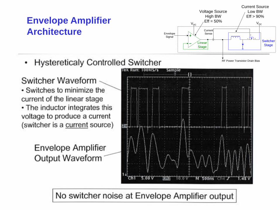
Envelope Amplifier
Architecture Envelope
Signal
Current
Sense
RF Power Transistor Drain Bias
Linear
Stage
g
s d
VDC
Switcher
Stage
Voltage Source
High BW
Eff = 50%
Current Source
Low BW
Eff > 90%
Envelope Amplifier: Overall Efficiency ~ 85%
BW = 50 MHz
VDC
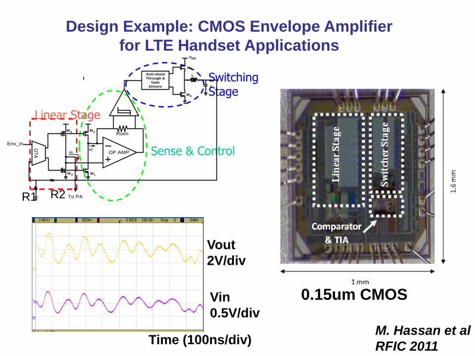
Design Example: CMOS Envelope Amplifier
for LTE Handset Applications
Linear Stage
Switching Stage
Sense & Control
Anti-shoot
Through &
Gate
Drivers
M6
V DD
L
M1
M2
M4
M3
OT
A
Env_in
To PA
Rsen
M5
OP AMP
c
idia
R2 R1
M. Hassan et al
RFIC 2011
0.15um CMOS
Time (100ns/div)
Vin
0.5V/div
Vout
2V/div
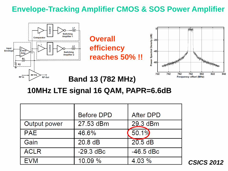
10MHz LTE signal 16 QAM, PAPR=6.6dB
Band 13 (782 MHz)
Envelope-Tracking Amplifier CMOS & SOS Power Amplifier
Overall
efficiency
reaches 50% !!
CSICS 2012
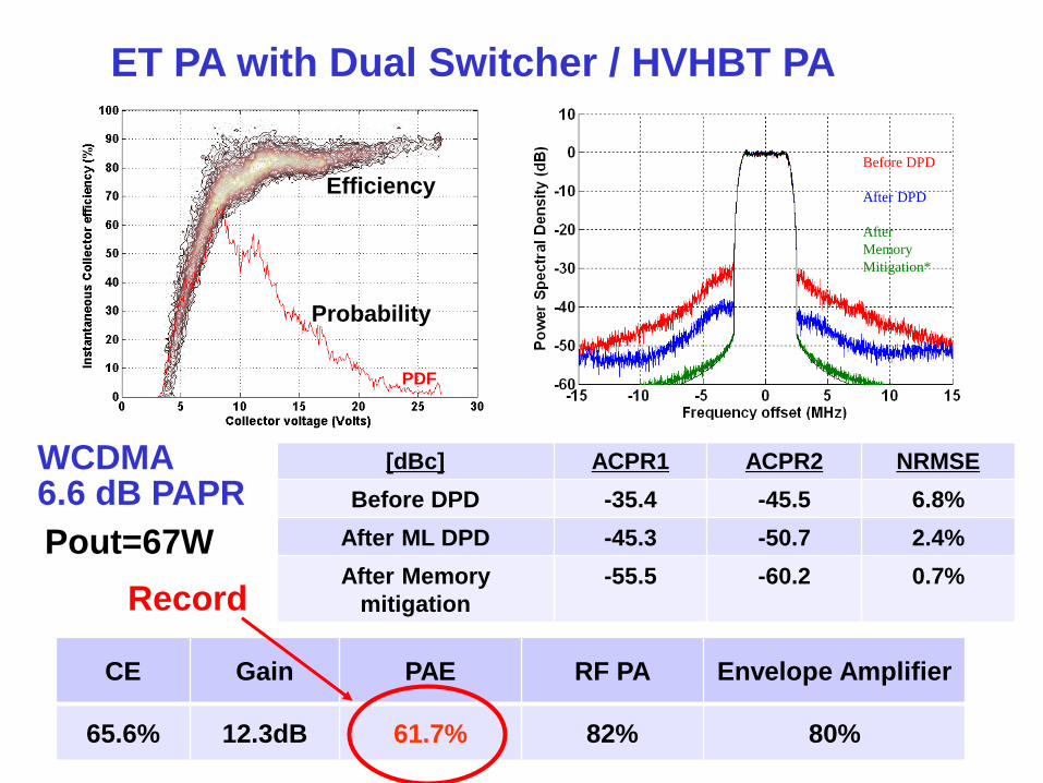
[dBc] ACPR1 ACPR2 NRMSE
Before DPD -35.4 -45.5 6.8%
After ML DPD -45.3 -50.7 2.4%
After Memory
mitigation
-55.5 -60.2 0.7%
ET PA with Dual Switcher / HVHBT PA
CE Gain PAE RF PA Envelope Amplifier
65.6% 12.3dB 61.7% 82% 80%
WCDMA 6.6 dB PAPR
Before DPD
After DPD
After
Memory
Mitigation*
Record
Efficiency
Probability
Pout=67W
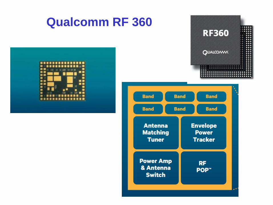
Qualcomm RF 360