Embed Size (px)
Citation preview
CPC - H03F - 2017.08
H03F
AMPLIFIERS (measuring, testing G01R; optical parametric amplifiers G02F;circuit arrangement with secondary emission tubes H01J 43/30; masers, lasersH01S; control of amplification H03G; coupling arrangements independent ofthe nature of the amplifiers, voltage dividers H03H; amplifiers capable only ofdealing with pulses H03K; repeater circuits in transmission lines H04B 3/36,H04B 3/58; application of speech amplifiers in telephonic communicationH04M 1/60, H04M 3/40)
Definition statement
This place covers:
• Linear amplification, there being linear relationship between the amplitudes of input and output,and the output having substantially the same waveform as the input;
• Dielectric amplifiers, magnetic amplifiers, and parametric amplifiers when used as oscillators orfrequency-changers;
• Constructions of active elements of dielectric amplifiers and parametric amplifiers if no provisionexists elsewhere.
The user is otherwise referred to the IPC definitions for the individual main groups of H03F whichfollow hereinafter, although the following IPC groups are not used in the internal ECLA classificationscheme. Subject matter covered by these groups is classified in the following ECLA groups: H03F1/44covered by H03F 1/42 H03F1/46 covered by H03F 1/42 H03F3/18 covered by H03F 3/00 H03F3/32covered by H03F 3/30 H03F7/06 covered by H03F 7/00
Provisions that are valid at a general level (e.g. of a kind appropriate to more than one of the maingroups) are provided in the sections that follow.
The following list is intended to assist the user.
Relationships with other classification places
The structural association with elements coupled with amplifiers can be classified either in H03F orin the subclass covering the element (or in both the subclasses), depending on which aspect is morerelevant.
In particular H03F units represented as "black boxes" in a specific application (e.g. a servo loopcontrol circuit for a motor) are in general not classified in H03F, unless a specific technical effect whichis relevant for H03F is achieved (e.g. linearity of amplification).
Components covered by specific subclasses (e.g. resistors, inductors, transmission lines, etc.):
• if relevant for their structural association with the amplifier are classified in H03F;
• if relevant only per se are not classified in H03F, but in the specific subclass.
References
Limiting references
This place does not cover:
Biomedical instrumentation amplifiers A61B 5/04
Measuring, testing G01R
Optical parametric amplifiers G02F
Analog calculators G06G 7/12
Musical instrument amplifiers (case of linear amplification) G10H
1
H03F (continued) CPC - H03F - 2017.08
Sound producing devices G10K
Sense amplifiers G11C 7/06
Variable transformers H01F 29/14
Circuit arrangements with secondary emission tubes H01J 43/30
Aerials H01Q
Masers, lasers H01S
Transference of modulation from one carrier to another H03D 7/00
Amplifiers capable only of dealing with pulses, electronic switches,comparators, logic circuits, PWM signals
H03K
Analog transmitter circuits H04B 1/04
Analog receiver circuits H04B 1/16
Repeater circuits in transmission lines H04B 3/36, H04B 3/58
Optical transmitters H04B 10/00
Optical receivers H04B10/158
Frequency-division multiplex system H04J 1/00, H04J 1/00
Baseband systems H04L 25/00
Digital transmitters H04L 27/04
Digital receivers H04L 27/06
Application of speech amplifiers in telephonic communication H04M 1/60, H04M 3/40
Television systems with video amplifiers, IF amplifiers H04N 5/148, H04N 9/647
Circuits for transducers, public address systems H04R 3/00, H04R 27/00
Informative references
Attention is drawn to the following places, which may be of interest for search:
Semiconductors or other solid state devices H01L
Nanotube transistors H01L 51/00
Waveguides, resonators H01P
Emergency protection circuit arrangements H02H
AC/DC, DC/DC, AC/AC power converters H02M
Generation of oscillations H03B
Modulation H03C
Demodulation H03D
Control of amplification H03G
Coupling arrangements independent of the nature of the amplifiers,voltage dividers, attenuators
H03H
Control of generators of electronic oscillations or pulses, e.g. phaselocked loops
H03L
A/D and D/A converters, sigma delta modulators H03M
2
H03F (continued) CPC - H03F - 2017.08
Special rules of classification
As general remark, it must be noted that multiple classification symbols may be given. The philosophyis to classify documents in several sub-groups as the case may be, i.e. the classifier should not stopthe classification task once that the first suitable EC symbol is found, but he should continue to assignEC symbols until all the aspects have been properly classified.
The subclass has a very large number of related technical areas, e.g.:
• "application" fields such as transmitters, receivers, voltage regulators, multimedia devices, etc.
Indexing Code orthogonal classification
In addition to one or more classification symbols relating to the invention information,where appropriate, one or more Indexing Code symbols relating to orthogonal classification(H03F 2200/03 - H03F 2200/555), i.e. covering aspects which are spanning over one or more groups,should be allocated for the following ranges:
H03F 1/00 H03F 1/565
H03F 3/181 H03F 3/213
H03F 3/24 H03F 3/72
Vacuum tube amplifiers classification
The following IPC groups, which are mostly related to discharge tube amplifiers or general typeamplifiers, are used to classify circuit topologies based also on vacuum tubes, valve amplifiers, due tohistorical reasons (see vacuum tube amplifier in the "Glossary of terms" section below):
H03F 1/04 H03F 1/07
H03F 1/13
H03F 1/16
H03F 1/20
H03F 1/24
H03F 1/28
H03F 1/33
H03F 1/36
H03F 1/40
H03F 1/50
H03F 1/54
H03F 3/02
H03F 3/181
H03F 3/189
H03F 3/22
H03F 3/28
H03F 3/36
3
H03F (continued) CPC - H03F - 2017.08
H03F 3/40
H03F 3/44
H03F 3/48
H03F 3/52
H03F 3/64
Glossary of terms
In this place, the following terms or expressions are used with the meaning indicated:
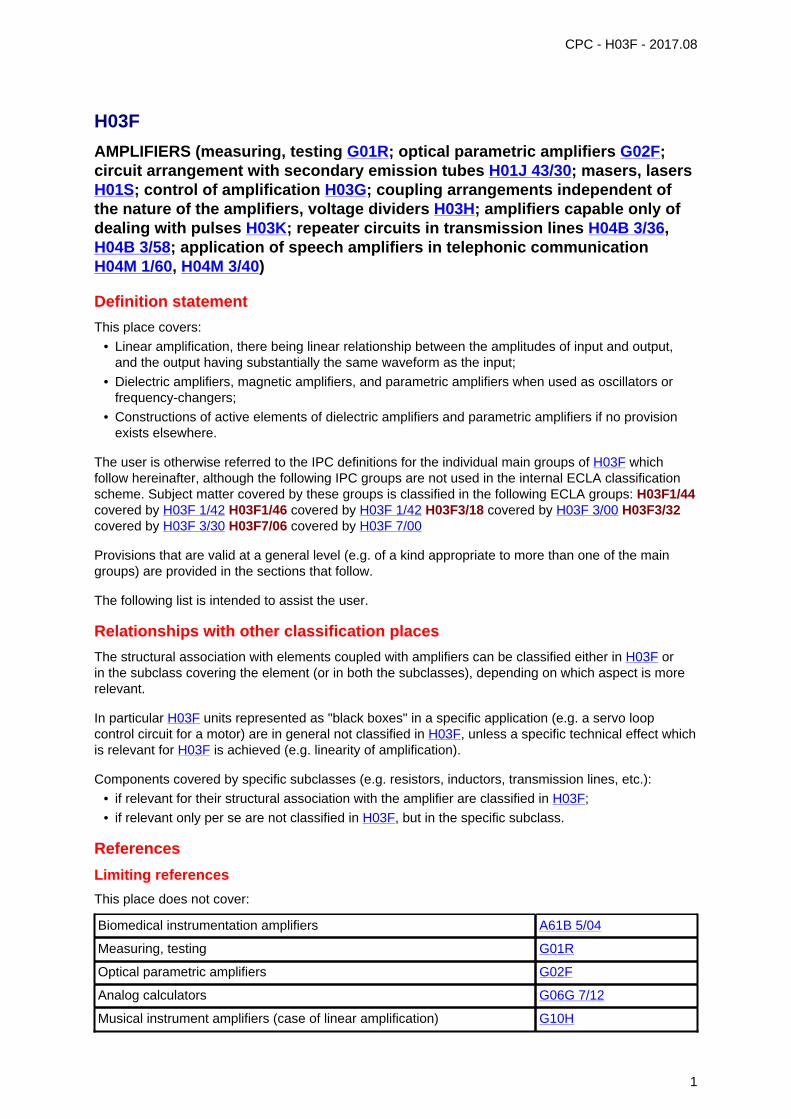
Class A
Amplifying devices operating in class Aconduct in their linear range over the whole of the input cycle.
Class B
Amplifying devices operating in class Bconduct in their linear range half of the time and are turned off forthe other half
Class AB
Amplifying devices operating in class ABconduct in their linear range for more than half of the time
Class C
Amplifying devices operating in class Cconduct in their linear range for less than half of the time
Class D
In the basic class-D amplifier the input signal is convertedinto a sequence of pulse width modulated (PWM) pulses via acomparator (C). Said PWM sequence is amplified via switchingamplifying devices and filtered in order to produce an amplifiedreplica of said input signal at the output.
4
H03F (continued) CPC - H03F - 2017.08
Class E
The basic topology of class-E amplifier includes a transistor T,operated as a switch, a shunt capacitor (C1) which includes theintrinsic transistor output capacitance, RF choke inductor (L1), aload resistor R, a series resonance circuit (Co, Lo), and an excessinductance XL. The reactive elements shape the current andvoltage waveforms across the transistor as shown. Thus as currentflows, there is essentially no voltage across the device and a highlyefficient switching power amplifier is achieved.
Class F
In realizing a class F amplifier, the active device operates primarilyas a switch and the output network, generally, is designedto yield short circuit impedances at even harmonics of thefundamental frequency and to yield open circuit impedances at oddharmonics of the fundamental frequency. (drawing extracted fromUS4717884)
5
H03F (continued) CPC - H03F - 2017.08
Class G
The Class G amplifiers(which use "rail switching" to decrease power consumptionand increase efficiency) provide several power rails at differentvoltages (HV, LV) and switch between them as the signal outputapproaches each level. Thus, the amplifier increases efficiency byreducing the wasted power at the output transistors.
Class H
Class-H amplifiers take the idea ofclass G one step further creating an infinitely variable supply rail.This is done by modulating the supply rails (VCC, VEE) so that therails are only a few volts larger than the output signal at any giventime. The output stage operates at its maximum efficiency all thetime. Switched-mode power supplies can be used to create thetracking rails.
Class S
Class S amplifiers are used essentially for RF transmitters oras tracking power supply building blocks. The basic architectureconsists of a modulator, e.g., of delta-sigma type, a fast broadbandswitch-mode amplifier, and an advanced filter at the output. Thebig advantage of the concept is that it can potentially be driven witha digital input without A/D conversion at the input.
6
H03F (continued) CPC - H03F - 2017.08
Totem pole
Amplifier with two or more amplifyingelements having their DC paths in series with the load, the controlelectrode of each element being excited by at least part of theinput signal (drawing extracted from US3986132).
Distributed amplifier
The input/output terminalsof the amplifying elements are connected in series throughrespective distributed elements. (drawing extracted fromUS2005285680)
Doherty Amplifier
Amplifier using a main andone or several auxiliary peaking amplifiers wherein the load isconnected to the main amplifier using an impedance inverter.(drawing extracted from WO2011097114)
Push Pull
The amplifying devices areeach used for amplifying the opposite halves of the input signal.
7
H03F (continued) CPC - H03F - 2017.08
Single Ended Push Pull
Push pull amplifier whereinthe output terminals of the amplifying elements are tied together asa single ended output without additional balun elements.
Differential amplifier
the basic differential amplifieramplifies the difference between two voltages; the outputvoltage is determined according to the following equation:
wherein Ac is thecommon mode gain and Ad is the differential mode gain.
Common mode rejection ratio the common-mode rejection ratio (CMRR) indicates the abilityof the amplifier to accurately cancel voltages that are commonto both inputs. The common-mode rejection ratio is defined as:
8
H03F (continued) CPC - H03F - 2017.08
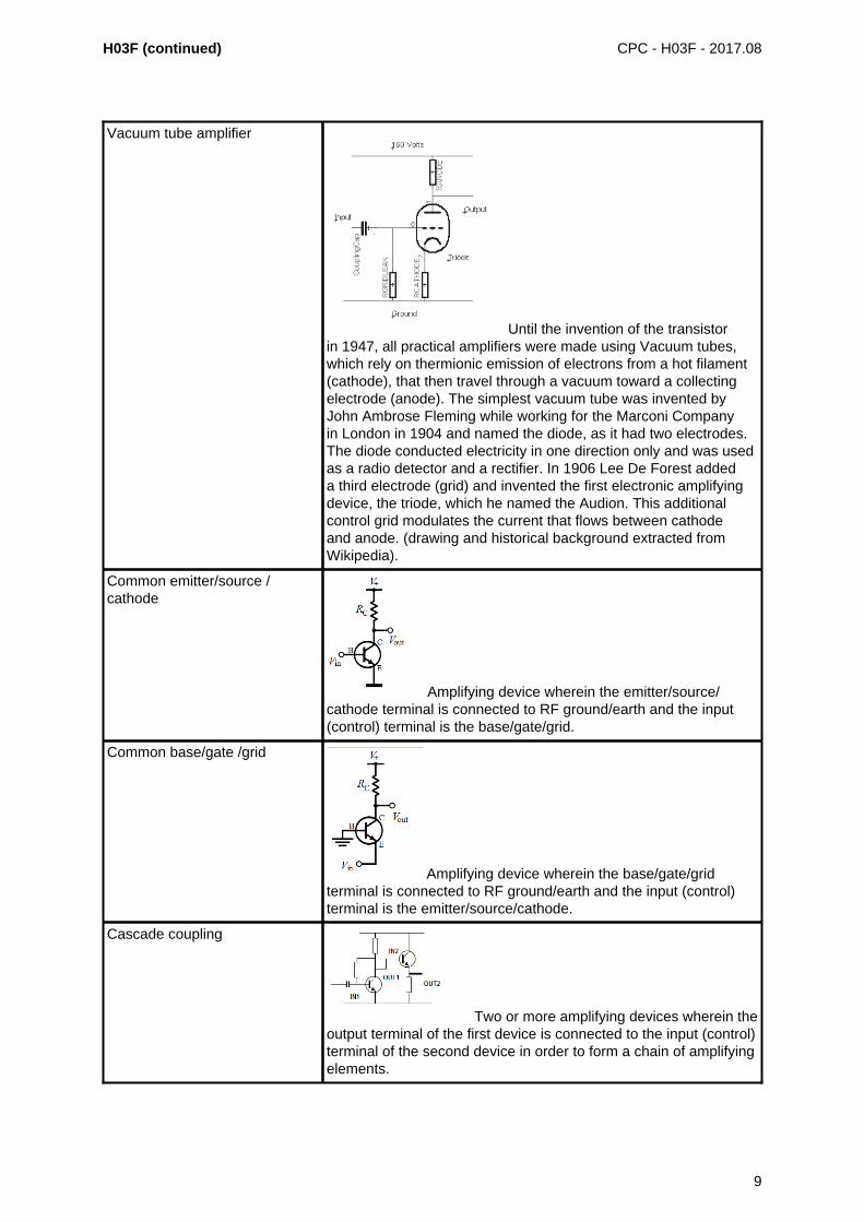
Vacuum tube amplifier
Until the invention of the transistorin 1947, all practical amplifiers were made using Vacuum tubes,which rely on thermionic emission of electrons from a hot filament(cathode), that then travel through a vacuum toward a collectingelectrode (anode). The simplest vacuum tube was invented byJohn Ambrose Fleming while working for the Marconi Companyin London in 1904 and named the diode, as it had two electrodes.The diode conducted electricity in one direction only and was usedas a radio detector and a rectifier. In 1906 Lee De Forest addeda third electrode (grid) and invented the first electronic amplifyingdevice, the triode, which he named the Audion. This additionalcontrol grid modulates the current that flows between cathodeand anode. (drawing and historical background extracted fromWikipedia).
Common emitter/source /cathode
Amplifying device wherein the emitter/source/cathode terminal is connected to RF ground/earth and the input(control) terminal is the base/gate/grid.
Common base/gate /grid
Amplifying device wherein the base/gate/gridterminal is connected to RF ground/earth and the input (control)terminal is the emitter/source/cathode.
Cascade coupling
Two or more amplifying devices wherein theoutput terminal of the first device is connected to the input (control)terminal of the second device in order to form a chain of amplifyingelements.
9
H03F (continued) CPC - H03F - 2017.08
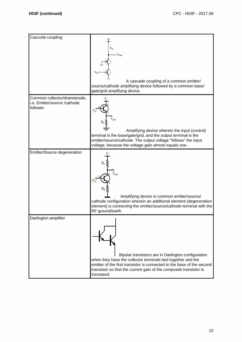
Cascode coupling
A cascade coupling of a common emitter/source/cathode amplifying device followed by a common base/gate/grid amplifying device.
Common collector/drain/anode,i.e. Emitter/source /cathodefollower
Amplifying device wherein the input (control)terminal is the base/gate/grid, and the output terminal is theemitter/source/cathode. The output voltage "follows" the inputvoltage, because the voltage gain almost equals one.
Emitter/Source degeneration
Amplifying device in common emitter/source/cathode configuration wherein an additional element (degenerationelement) is connecting the emitter/source/cathode terminal with theRF ground/earth.
Darlington amplifier
Bipolar transistors are in Darlington configurationwhen they have the collector terminals tied together and theemitter of the first transistor is connected to the base of the secondtransistor so that the current gain of the composite transistor isincreased.
10
H03F (continued) CPC - H03F - 2017.08
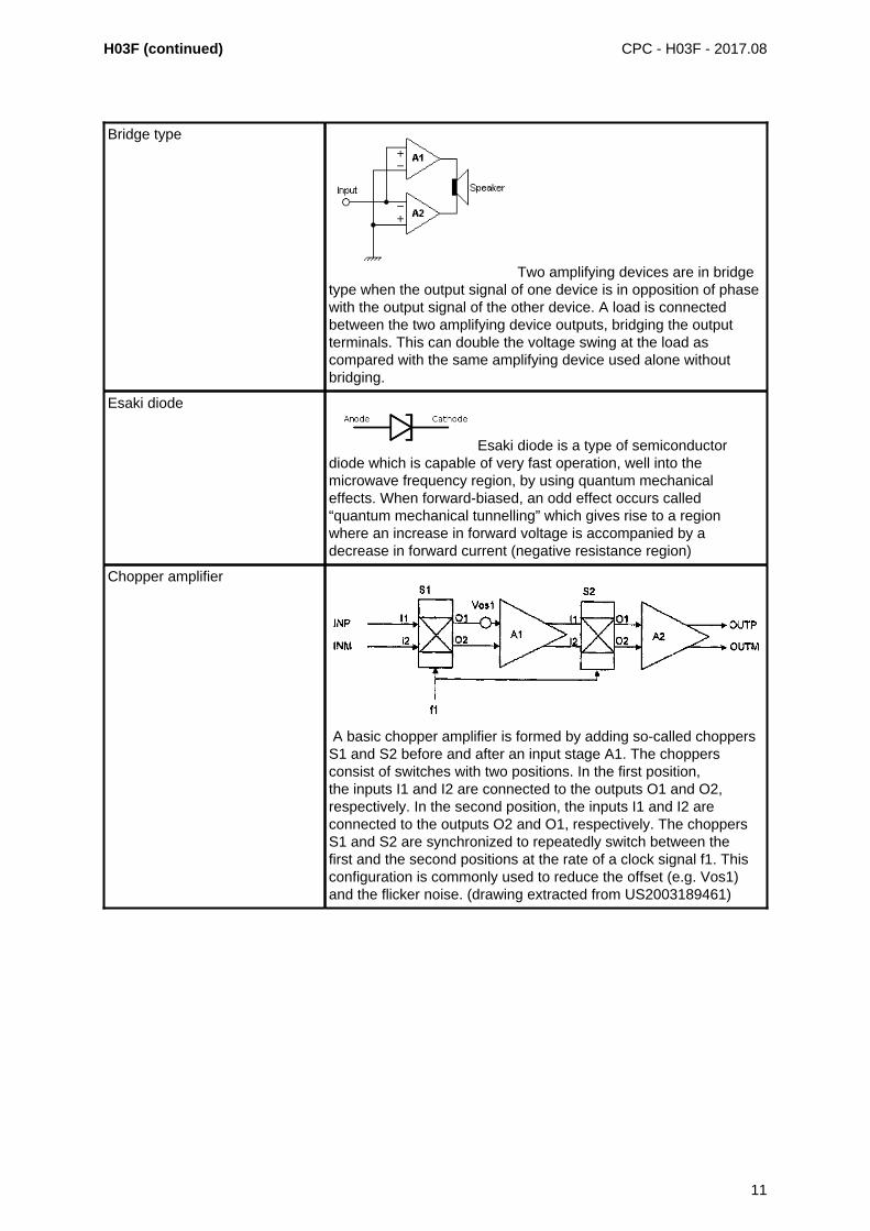
Bridge type
Two amplifying devices are in bridgetype when the output signal of one device is in opposition of phasewith the output signal of the other device. A load is connectedbetween the two amplifying device outputs, bridging the outputterminals. This can double the voltage swing at the load ascompared with the same amplifying device used alone withoutbridging.
Esaki diode
Esaki diode is a type of semiconductordiode which is capable of very fast operation, well into themicrowave frequency region, by using quantum mechanicaleffects. When forward-biased, an odd effect occurs called“quantum mechanical tunnelling” which gives rise to a regionwhere an increase in forward voltage is accompanied by adecrease in forward current (negative resistance region)
Chopper amplifier
A basic chopper amplifier is formed by adding so-called choppersS1 and S2 before and after an input stage A1. The choppersconsist of switches with two positions. In the first position,the inputs I1 and I2 are connected to the outputs O1 and O2,respectively. In the second position, the inputs I1 and I2 areconnected to the outputs O2 and O1, respectively. The choppersS1 and S2 are synchronized to repeatedly switch between thefirst and the second positions at the rate of a clock signal f1. Thisconfiguration is commonly used to reduce the offset (e.g. Vos1)and the flicker noise. (drawing extracted from US2003189461)
11
H03F (continued) CPC - H03F - 2017.08
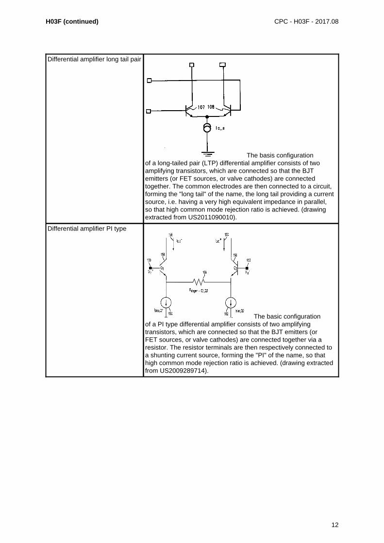
Differential amplifier long tail pair
The basis configurationof a long-tailed pair (LTP) differential amplifier consists of twoamplifying transistors, which are connected so that the BJTemitters (or FET sources, or valve cathodes) are connectedtogether. The common electrodes are then connected to a circuit,forming the "long tail" of the name, the long tail providing a currentsource, i.e. having a very high equivalent impedance in parallel,so that high common mode rejection ratio is achieved. (drawingextracted from US2011090010).
Differential amplifier PI type
The basic configurationof a PI type differential amplifier consists of two amplifyingtransistors, which are connected so that the BJT emitters (orFET sources, or valve cathodes) are connected together via aresistor. The resistor terminals are then respectively connected toa shunting current source, forming the "PI" of the name, so thathigh common mode rejection ratio is achieved. (drawing extractedfrom US2009289714).
12
H03F (continued) CPC - H03F - 2017.08
Pseudo differential amplifier
The basic configuration of a pseudodifferential amplifier consists of two amplifying transistors, whereinthe BJT emitters (or FET sources, or valve cathodes) are notconnected together but directly coupled to the ground. Thus, sincethe difference between I1 and I2 is output in proportion to thedifference between gate signals Va, Vb, the configuration acts asa differential transconductance amplifier (drawing extracted fromUS2009115461).
Reflex amplifier
In a basic reflex amplifier anAC input signal is amplified and then rectified and, using thesame circuit elements, the fed back resultant rectified DC signalis again amplified. The reflex circuit thus achieves two stagesof amplification, plus rectification, in a single stage. (drawingextracted from US2863066).
13
H03F (continued) CPC - H03F - 2017.08
Travelling Wave Tube Amplifier(TWTA)
A travelling wave tube (TWT) integrated with a regulated powersupply and protection circuits is referred to as a travelling wave-tube amplifier (TWTA). The basic configuration of a TWT is anelongated vacuum tube with an electron gun (a heated cathodethat emits electrons) at one end. A magnetic containment fieldaround the tube focuses the electrons into a beam, which thenpasses down the middle of an RF circuit (wire helix or coupledcavity) that stretches from the RF input to the RF output, theelectron beam finally striking a collector at the other end. Adirectional coupler, which can be either a waveguide or anelectromagnetic coil, fed with the low-powered radio signal thatis to be amplified, is positioned near the emitter, and induces acurrent into the helix. The RF circuit acts as a delay line, in whichthe RF signal travels at near the same speed along the tube as theelectron beam. The electromagnetic field due to the RF signal inthe RF circuit interacts with the electron beam, causing bunchingof the electrons (an effect called velocity modulation), and theelectromagnetic field due to the beam current then induces morecurrent back into the RF circuit (i.e. the current builds up and thusis amplified as it passes down). A second directional coupler,positioned near the collector, receives an amplified version of theinput signal from the far end of the RF circuit. (drawing extractedfrom US5500621).
14
H03F (continued) CPC - H03F - 2017.08
Klystron
A klystron amplifies RF signals by converting the kinetic energyin a DC electron beam into radio frequency power. A beam ofelectrons is produced by a thermionic cathode (a heated pelletof low work function material), and accelerated by high-voltageelectrodes (typically in the tens of kilovolts). This beam is thenpassed through an input cavity. RF energy is fed into the inputcavity at, or near, its natural frequency to produce a voltage whichacts on the electron beam. The electric field causes the electronsto bunch: electrons that pass through during an opposing electricfield are accelerated and later electrons are slowed, causing thepreviously continuous electron beam to form bunches at the inputfrequency. To reinforce the bunching, a klystron may containadditional "buncher" cavities. The RF current carried by the beamwill produce an RF magnetic field, and this will in turn excite avoltage across the gap of subsequent resonant cavities. In theoutput cavity, the developed RF energy is coupled out. The spentelectron beam, with reduced energy, is captured in a collector.
Envelope Elimination andRestoration (EER)
TheEnvelope elimination and restoration technique was first proposedin 1952 by L.R. Kahn as a way to linearise nonlinear amplifiers.In Kahn's approach, an RF input signal is processed by twoparallel paths. In one path, the envelope of the RF input signal is"eliminated" using a limiting amplifier that removes any amplitudemodulation and which provides a phase modulated signal. In theother path, the RF input signal envelope is detected, amplified,and applied to the PA as an amplitude modulating power supplyvoltage. The EER technique allows the phase modulated signal tobe amplified with high efficiency using a saturated power amplifier,which has an amplitude modulating power supply voltage, in orderto restore the RF signal envelope at the output of said amplifierand to obtain linear amplification of the RF input signal.
15
H03F (continued) CPC - H03F - 2017.08
Envelope Tracking (ET)
In the Envelope Trackingconfiguration, the power amplifier is fed with a fully-modulated RFsignal (RFin) at the input and supplied with a modulated drain bias(Vout) in accordance with the envelope of the modulated signal(Venv). As a result, the power amplifier at all times is kept nearsaturation where the efficiency is highest. (drawing extracted fromUS7808323)
Charge amplifier
A chargeamplifier is a current integrator driven by an electrical source withcapacitive nature such as a piezoelectric sensor. Contrary towhat its name may suggest, a charge amplifier does not amplifythe electric charge present at its input (it can amplify only theexciting input voltage). The charge amplifier just transfers the inputcharge to another reference capacitor and produces an outputvoltage equal to the voltage across the reference capacitor. Thusthe output voltage is proportional to the charge of the referencecapacitor and, respectively, to the input charge; hence the circuitacts as a charge-to-voltage converter. Charge amplifiers areusually constructed using op-amps with a feedback capacitor.(drawing extracted from GB2381977)
Note: all the drawings of the present section, when not explicitly indicated, have been extracted fromWikipedia.
Synonyms and Keywords
In patent documents, the following abbreviations are often used:
RF Radio Frequency
HF High Frequency, Hoch-Frequenz (German). Haute Fréquence(French)
NF (German) Nieder-Frequenz (German)
NF Noise Figure
LF Low Frequency
16
H03F (continued) CPC - H03F - 2017.08
BF (French) Basse Fréquence (French)
LNA Low Noise Amplifier
MMIC Microwave Monolithic Integrated Circuit
IC Integrated Circuit
OP-AMP Operational Amplifier
FET Field Effect Transistor
TEC (French) Transistor à Effet de Champ (French)
AC Alternate Current
DC Direct Current
DAT Distributed Active Transformer
SEPP Single Ended Push Pull
BALUN Balanced/Unbalanced or Unbalanced/Balanced
EMI Electromagnetic Interference
ESD Electro Static Discharge
TD Time Domain
PD Predistorter
BiFET Bipolar and Field Effect Transistor
CMMR Common-Mode Rejection Ratio
CCCS Current Controlled Current Source
CCVS Current Controlled Voltage Source
VCVS Voltage Controlled Voltage Source
VCCS Voltage Controlled Current Source
TIA Trans-Impedance Amplifier
OTA Operational Transconductance Amplifier
TWT Travelling Wave Tube
PA Power Amplifier
DPA Doherty Power Amplifier
MMPA Multi-Mode Power Amplifier
TWTA Travelling Wave Tube Amplifier
LTP Long Tailed Pair
EER Envelope Elimination and Restoration
ET Envelope Tracking
BTL Bridged Tied Load
17
CPC - H03F - 2017.08
H03F 1/00
Details of amplifiers with only discharge tubes, only semiconductor devices oronly unspecified devices as amplifying elements
Definition statement
This place covers:
Details of amplifiers with only discharge tubes, only semiconductor devices or only unspecifieddevices as amplifying elements, wherein said details are addressing a specific technical effect for theamplification:
Raise the efficiency
Reduce detrimental influences of internal impedances of the amplifying elements
Reduce influence of noise generated by amplifying elements
Reduce influence of variations of temperature or supply voltage or other physical parameters
Reduce non-linear distortion (except when using negative feedback)
Negative feedback with or without positive feedback
Positive feedback without negative feedback
Bandwidth extension
Protection
Modification of input or output impedances
The technical effect is specified according to the IPC definitions for the individual subgroups ofH03F 1/00 which follow hereinafter.
Special rules of classification
A document may be temporarily allocated in the main group H03F 1/00 only for EPO internalcirculation, e.g. to receive it from neighbouring field classifiers via the classification code.
H03F 1/02
Modifications of amplifiers to raise the efficiency, e.g. gliding Class A stages,use of an auxiliary oscillation
Definition statement
This place covers:
Modifications of amplifiers to raise the efficiency, wherein said modification comprises the followingtechniques:
dynamic bias control based on the input/output signal
supply control based on the input/output signal
selection of one or more amplifiers from a plurality of amplifier
reduction of the number of DC current paths
use of particular circuit topologies, e.g. Doherty amplifier, LINC Amplifier
18
H03F 1/02 (continued) CPC - H03F - 2017.08
use of discharge tube amplifiers acting also as modulators.
References
Limiting references
This place does not cover:
Transmitter circuits with power amplifiers having gain or transmissionpower control, with means for improving efficiency
H04B 2001/0416,H04B 2001/045
Informative references
Attention is drawn to the following places, which may be of interest for search:
Amplitude modulation by converting angle modulation to amplitudemodulation
H03C 1/50
Gain control details, gain control by varying the supply voltage, gaincontrol dependent on the supply voltage
H03G 1/00, H03G 3/004,H03G 3/007
Transmission power control H04W 52/04
H03F 1/08
Modifications of amplifiers to reduce detrimental influences of internalimpedances of amplifying elements (wide-band amplifiers with inter-stagecoupling networks incorporating these impedances H03F 1/42; eliminatingtransit-time effects in vacuum tubes H01J 21/34)
Definition statement
This place covers:
Modification of amplifiers to achieve frequency stabilisation or signal isolation among amplifyingstages, wherein said modification comprises the following techniques:
use of particular circuit topologies, e.g. transimpendance amplifier, cascode amplifier
use of amplifying elements with multiple electrode connections
use of attenuating means
use of neutralising means, e.g. Miller effect compensation circuitry, pole/zero cancellations in thetransfer function
use of distributed coupling
References
Limiting references
This place does not cover:
Eliminating transit-time effects in vacuum tubes H01J 21/34
19
H03F 1/08 (continued) CPC - H03F - 2017.08
Application-oriented references
Examples of places where the subject matter of this place is covered when specially adapted, used fora particular purpose, or incorporated in a larger system:
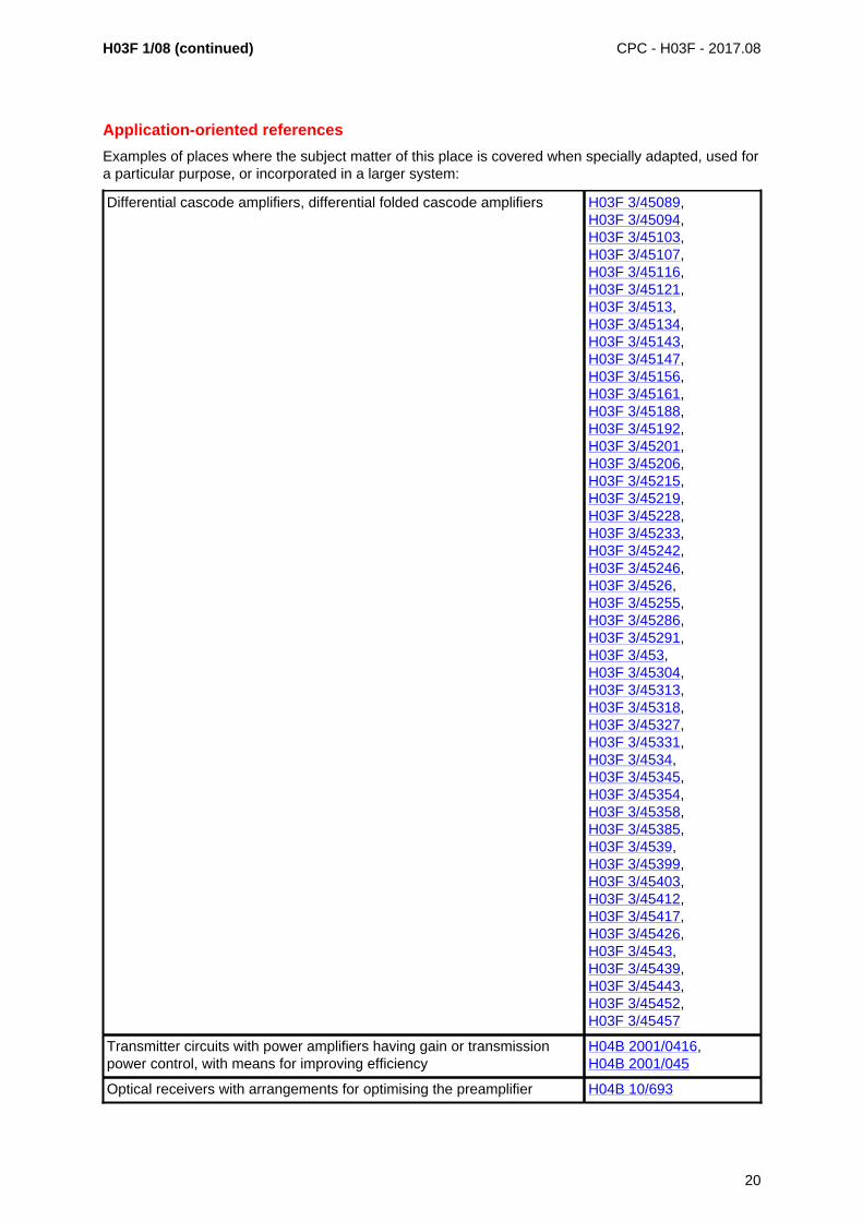
Differential cascode amplifiers, differential folded cascode amplifiers H03F 3/45089,H03F 3/45094,H03F 3/45103,H03F 3/45107,H03F 3/45116,H03F 3/45121,H03F 3/4513,H03F 3/45134,H03F 3/45143,H03F 3/45147,H03F 3/45156,H03F 3/45161,H03F 3/45188,H03F 3/45192,H03F 3/45201,H03F 3/45206,H03F 3/45215,H03F 3/45219,H03F 3/45228,H03F 3/45233,H03F 3/45242,H03F 3/45246,H03F 3/4526,H03F 3/45255,H03F 3/45286,H03F 3/45291,H03F 3/453,H03F 3/45304,H03F 3/45313,H03F 3/45318,H03F 3/45327,H03F 3/45331,H03F 3/4534,H03F 3/45345,H03F 3/45354,H03F 3/45358,H03F 3/45385,H03F 3/4539,H03F 3/45399,H03F 3/45403,H03F 3/45412,H03F 3/45417,H03F 3/45426,H03F 3/4543,H03F 3/45439,H03F 3/45443,H03F 3/45452,H03F 3/45457
Transmitter circuits with power amplifiers having gain or transmissionpower control, with means for improving efficiency
H04B 2001/0416,H04B 2001/045
Optical receivers with arrangements for optimising the preamplifier H04B 10/693
20
H03F 1/08 (continued) CPC - H03F - 2017.08
Informative references
Attention is drawn to the following places, which may be of interest for search:
Wide-band amplifiers with inter-stage coupling networks incorporatingthese impedences
H03F 1/42
Distributed amplifiers using coupling networks with distributed constants H03F 3/605
Gain control in emitter coupled or cascode amplifiers H03G 1/0023
Modifications of control circuit to reduce distortion caused by control H03G 1/04
Muting circuits H03G 3/26, H03G 3/34
Amplitude limiters H03G 11/00
Glossary of terms
In this place, the following terms or expressions are used with the meaning indicated:
Current steering cascode cascode amplifier formed by at least two common gate transistorswhich are both coupled to the drain terminal of the input commonsource transistor, in order to steer the current at that terminalamong different paths.
Synonyms and Keywords
In patent documents, the following words/expressions are often used with the meaning indicated:
"cascade" "cascode".
H03F 1/26
Modifications of amplifiers to reduce influence of noise generated byamplifying elements
References
Limiting references
This place does not cover:
Modifications of amplifiers to reduce influence of variations of supplyvoltage in case of switching on or off of a power supply, i.e. popping noisereduction
H03F 1/305
Constructional modification of discharge tubes amplifiers H01J 23/11
Application-oriented references
Examples of places where the subject matter of this place is covered when specially adapted, used fora particular purpose, or incorporated in a larger system:
Chopper amplifiers H03F 3/38
Transmitter circuits with means for limiting noise H04B 1/0475
21
CPC - H03F - 2017.08
H03F 1/30
Modifications of amplifiers to reduce influence of variations of temperatureor supply voltage {or other physical parameters (in differential amplifiersH03F 3/45479)}
Definition statement
This place covers:
Modifications of amplifiers to reduce influence of variations of temperature or supply voltage, or otherphysical parameters, wherein said modifications comprise:
bias stabilisation circuits
drifting protection circuits
using a switching device and eventually digital means
case of switching on or off a power supply
case of push-pull configuration
References
Limiting references
This place does not cover:
Differential amplifiers characterised by the way of common mode signalrejection
H03F 3/45479
Application-oriented references
Examples of places where the subject matter of this place is covered when specially adapted, used fora particular purpose, or incorporated in a larger system:
Push-pull amplifiers H03F 3/26
Single-ended push-pull (SEPP) H03F 3/30
Informative references
Attention is drawn to the following places, which may be of interest for search:
Voltage, current regulators G05F 1/10, G05F 3/02
Muting circuits H03G 3/26, H03G 3/34
Glossary of terms
In this place, the following terms or expressions are used with the meaning indicated:
Popping noise audible noise which is present when switching on or off the powersupply
22
H03F 1/30 (continued) CPC - H03F - 2017.08
Synonyms and Keywords
In patent documents the following expressions are often used as synonyms:
Popping noise pop effect, plop noise, clic
H03F 1/32
Modifications of amplifiers to reduce non-linear distortion (by negativefeedback H03F 1/34)
Definition statement
This place covers:
Modifications of amplifiers to reduce non-linear distortion, wherein said modifications comprise:
using feedforward circuits
using predistortion circuits, which are implemented with feedback, or via multiple paths, or in audioamplifiers, or with nonlinear elements, or acting on cartesian and polar parameters
case of differential amplifiers
case of single ended push pull amplifiers
References
Limiting references
This place does not cover:
Modifications of amplifiers to reduce non-linear distortion by negativefeedback
H03F 1/34
Application-oriented references
Examples of places where the subject matter of this place is covered when specially adapted, used fora particular purpose, or incorporated in a larger system:
Analog transmitter circuits with power amplifiers with linearisation usingpredistortion and using feed-forward
H04B 2001/0425,H04B 2001/0441
Analog transmitter circuits with means for limiting distortions H04B 1/0483,H04B 1/0475
Digital transmitters using predistortion H04L 27/367
Special rules of classification
Indexing Code orthogonal classification
In addition to one or more classification symbols relating to the invention information,where appropriate, one or more Indexing Code symbols relating to orthogonal classification(H03F 2201/3203 - H03F 2201/3236), i.e. covering aspects which are spanning over one or more ECsubgroups, should be allocated for the following sub-groups range: H03F 1/32 - H03F 1/3241.
23
CPC - H03F - 2017.08
H03F 1/34
Negative-feedback-circuit arrangements with or without positive feedback(H03F 1/02 - H03F 1/30, H03F 1/38 - H03F 1/50, H03F 3/50 take precedence; {forrejection of common mode signals H03F 3/45479})
Definition statement
This place covers:
Negative-feedback-circuit arrangements with or without positive feedback, wherein said arrangementscomprises:
adaptations for reducing the non-linear distortion
hybrid or directional couplers
transformers.
References
Limiting references
This place does not cover:
Differential amplifiers for the rejection of common mode signals H03F 3/45479
Application-oriented references
Examples of places where the subject matter of this place is covered when specially adapted, used fora particular purpose, or incorporated in a larger system:
Analog transmitter circuits with means for limiting distortions H04B 1/0483,H04B 1/0475
H03F 1/38
Positive-feedback circuit arrangements without negative feedback
References
Informative references
Attention is drawn to the following places, which may be of interest for search:
Generation of oscillation H03B
H03F 1/42
Modifications of amplifiers to extend the bandwidth
Definition statement
This place covers:
Modifications of amplifiers to extend the bandwidth, wherein the modifications comprise:
periodic amplifiers
aperiodic amplifiers, i.e. wherein aperiodic means that there is no resonant circuit present.
24
H03F 1/42 (continued) CPC - H03F - 2017.08
References
Application-oriented references
Examples of places where the subject matter of this place is covered when specially adapted, used fora particular purpose, or incorporated in a larger system:
Pulse shaping by amplifying H03K 5/02
Analog transmitter circuits with means for limiting distortions H04B 1/0483,H04B 1/0475
Optical receivers with bandwidth control H04B 10/6932
Glossary of terms
In this place, the following terms or expressions are used with the meaning indicated:
Inductive peaking an inductor is placed in the amplifying circuit to extend thebandwidth of amplification.
H03F 1/52
Circuit arrangements for protecting such amplifiers {(monitoring arrangementsG01R 31/28; increasing reliability in communication systems, e.g. usingredundancy H04B 1/74)}
Definition statement
This place covers:
Circuit arrangements for protecting such amplifiers, wherein the arrangements comprises:
using redundant amplifying elements
using protective devices, e.g. diodes.
References
Limiting references
This place does not cover:
Protection from temperature drifting H03F 1/30
Vacuum tube testing G01R 31/25
Application-oriented references
Examples of places where the subject matter of this place is covered when specially adapted, used fora particular purpose, or incorporated in a larger system:
Monitoring arrangements G01R 31/28
Analog transmitter details for increasing reliability H04B 1/74
Informative references
Attention is drawn to the following places, which may be of interest for search:
Emergency protective circuit arrangements H02H 7/20
25
H03F 1/52 (continued) CPC - H03F - 2017.08
Over voltage protection in integrated circuits H02H 9/046
Frequency-division multiplex system with monitoring arrangements H04J 1/16, H04J 1/16
H03F 1/56
Modifications of input or output impedances, not otherwise provided for
Definition statement
This place covers:
Modifications of input or output impedances, not otherwise provided for, wherein said modificationsmay comprise:
matching and tuning circuits which are specifically designed for RF amplifiers
circuit adaptations in class E,F,E/F amplifiers.
References
Application-oriented references
Examples of places where the subject matter of this place is covered when specially adapted, used fora particular purpose, or incorporated in a larger system:
High frequency amplifiers H03F 3/189
Switching amplifiers in general H03F 3/217
Class E amplifiers H03F 3/2176
Amplifiers in which coupling networks have distributed constants H03F 3/60
Informative references
Attention is drawn to the following places, which may be of interest for search:
Matching with passive networks H03H 7/38
Matching with active networks H03H 11/28
H03F 3/00
Amplifiers with only discharge tubes or only semiconductor devices asamplifying elements
Definition statement
This place covers:
Electronic amplifiers based on tubes or semiconductors.
Amplifiers are classified according to topology (e.g., push-pull, emitter follower, differential) and/oraccording to use (e.g., LF, HF) and/or according to the amplifying element (e.g., tubes, tunnel diodes)and/or according to special functionality (e.g., multi-channel amplifiers, gated amplifiers).
Amplifiers with both tubes and semiconductors are classified in H03F 5/00.
Amplifiers based on other amplification principles such as magnetic, dielectric, mechanical/acoustic,superconductivity, etc., are classified in subgroups H03F 7/00-H03F 21/00.
26
H03F 3/00 (continued) CPC - H03F - 2017.08
Special rules of classification
A document may be temporarily allocated in the main group H03F 3/00 only for EPO internalcirculation, e.g. to receive it from neighbouring field classifiers via the classification code.
H03F 3/005
{using switched capacitors, e.g. dynamic amplifiers; using switched capacitorsas resistors in differential amplifiers (H03F 3/45 takes precedence)}
Definition statement
This place covers:
Amplifiers with switched capacitors used as synthesized resistors.
References
Limiting references
This place does not cover:
Amplifiers with charge pump- or other switched capacitor based powersupplies
H03F 1/02
Modulator/demodulator (chopper) amplifiers H03F 3/38
Chopper/auto-zero amplifiers for offset/noise reduction in differentialamplifiers
H03F 3/45
Informative references
Attention is drawn to the following places, which may be of interest for search:
Switched capacitor filters H03H 19/004
H03F 3/02
with tubes only (subsequent sub-groups take precedence)
References
Limiting references
This place does not cover:
Travelling wave tube amplifiers H03F 3/58
H03F 3/08
controlled by light
Definition statement
This place covers:
Amplifiers controlled by light, that is, for optically generated or transferred signals, e.g.,transimpedance amplifiers for fiber optic links, optical isolation amplifiers.
27
H03F 3/08 (continued) CPC - H03F - 2017.08
References
Application-oriented references
Examples of places where the subject matter of this place is covered when specially adapted, used fora particular purpose, or incorporated in a larger system:
Optical receivers H04B10/158
H03F 3/082
{with FET's (H03F 3/085 takes precedence)}
Definition statement
This place covers:
Amplifiers controlled by light, wherein the amplifier comprises FETs, e.g., JFET or CMOStransimpedance amplifiers for fiber optic links.
H03F 3/085
{using opto-couplers between stages}
Definition statement
This place covers:
Amplifiers controlled by light, wherein the amplifier comprises optically coupled stages, e.g., opticalisolating amplifiers.
H03F 3/087
{with IC amplifier blocks (H03F 3/085 takes precedence)}
Definition statement
This place covers:
Amplifiers controlled by light, wherein the amplifier has functional units such as op-amps, i.e., notshowing transistor level circuit details.
H03F 3/10
with diodes {(parametric amplifiers H03F 7/00)}
Definition statement
This place covers:
Amplifiers using diodes as an amplifying element, e.g., negative resistance diodes such as Gunn,IMPATT, Esaki (tunnel) diodes.
References
Limiting references
This place does not cover:
Switching amplifiers with freewheeling diodes H03F 3/217
28
CPC - H03F - 2017.08
H03F 3/12
with Esaki diodes
Definition statement
This place covers:
Amplifiers using Esaki (tunnel) diodes as an amplifying element.
H03F 3/14
with amplifying devices having more than three electrodes or more than twoPN junctions
Definition statement
This place covers:
Amplifiers with semiconductor amplifying devices having more than three electrodes, e.g., dual-gateMOSFETs, back-gate controlled MOSFETs, multi-emitter/collector BJTs. Note: by semiconductoramplifying devices is understood transistors; opamps and the like are not included, even if theyhave more than three terminals. Cascode amplifiers using dual-gate MOSFETs are classified inH03F 1/223.
H03F 3/16
with field-effect devices
Definition statement
This place covers:
Amplifiers with semiconductor field-effect amplifying devices, e.g., MOSFETs, JFETs, MESFETs.
H03F 3/165
{with junction-FET's}
Definition statement
This place covers:
Amplifiers with semiconductor junction field-effect amplifying devices, e.g., JFETs, MESFETs (but notMOSFETs).
H03F 3/181
Low frequency amplifiers, e.g. audio preamplifiers
Definition statement
This place covers:
Low frequency amplifiers, in most cases which are suitable for amplification of audio signals.
References
Informative references
Attention is drawn to the following places, which may be of interest for search:
Switching amplifiers H03F 3/217
29
H03F 3/181 (continued) CPC - H03F - 2017.08
Gain control in low frequency amplifiers H03G 3/3005,H03G 7/002, H03G 7/007,H03G 3/3089
Circuits for loudspeakers, microphones H04R 3/00
H03F 3/189
High frequency amplifiers, e.g. radio frequency amplifiers
Definition statement
This place covers:
High frequency amplifiers, e.g. radio frequency amplifiers, as detailed circuits or integrated circuitblocks.
References
Application-oriented references
Examples of places where the subject matter of this place is covered when specially adapted, used fora particular purpose, or incorporated in a larger system:
Amplifiers in which coupling networks have distributed constant H03F 3/60
IF amplifier circuits specially adapted for B&W TV H04N 5/4446
Informative references
Attention is drawn to the following places, which may be of interest for search:
Switching amplifiers H03F 3/217
High frequency adaptations of semiconductors H01L 23/66
Gain control in high frequency amplifiers, bandpass amplifiers H03G 3/3036,H03G 3/3052
Synonyms and Keywords
In patent documents, the following abbreviations are often used:
HBT Heterojunction Bipolar Transistor
HEMT High Electron Mobility Transistor
H03F 3/20
Power amplifiers, e.g. Class B amplifiers, Class C amplifiers(H03F 3/26 - H03F 3/30 take precedence)
Definition statement
This place covers:
Power amplifiers in general. e.g. class B amplifiers, Class C amplifiers, Class D amplifiers, ClassE amplifiers, Class F amplifiers, Class G amplifiers, Class H amplifiers, Class S amplifiers, orcombination of power amplifiers, or integrated circuits wherein the circuit topology is based on lumpedelements.
30
H03F 3/20 (continued) CPC - H03F - 2017.08
References
Limiting references
This place does not cover:
Push pull amplifiers H03F 3/26
Single ended push pull amplifiers H03F 3/30
Combination of amplifiers in which coupling networks have distributedconstant
H03F 3/602
Application-oriented references
Examples of places where the subject matter of this place is covered when specially adapted, used fora particular purpose, or incorporated in a larger system:
Multi-channel amplifiers H03F 3/68
Analog transmitters H04B 1/02
Digital transmitters H04L 27/04
Special rules of classification
Documents which are addressing a power amplifier in general are usually not classified in thissubgroup, but are allocated to the corresponding subgroups:
H03F 3/21
H03F 3/211
H03F 3/213
H03F 3/217
H03F 3/22
H03F 3/24
Indexing Code deep-indexing classification
In addition to one or more classification symbols relating to the invention information, whereappropriate, one or more Indexing Code symbols relating to deep-indexing classification(H03F 2203/21103 - H03F 2203/21196), i.e. covering embodiment aspects, should be allocated for thefollowing sub-group: H03F 3/211
H03F 3/217
Class D power amplifiers; Switching amplifiers
Definition statement
This place covers:
Amplifiers using switches as amplifying elements, e.g., class D audio amplifiers, class E, class F, classS RF amplifiers, as well as control circuitry such as PCM-PWM conversion etc.
31
H03F 3/217 (continued) CPC - H03F - 2017.08
References
Limiting references
This place does not cover:
Amplifiers with switched-mode (e.g., tracking) power supplies H03F 1/02
Chopper/auto-zero amplifiers H03F 3/38; H03F 3/45
Gated amplifiers H03F 3/72
Application-oriented references
Examples of places where the subject matter of this place is covered when specially adapted, used fora particular purpose, or incorporated in a larger system:
MRI gradient amplifiers G01R 33/3852
DC-AC converters H02M 3/00
Deaf-aid sets H04R 25/00
Stereophonic systems H04S
Special rules of classification
Multiple classification symbols may be given, e.g., a stereo full-bridge class D audio power amplifierwith protection means and anti pop-noise means would be classified in H03F 3/68, H03F 3/2173,H03F 1/52, H03F 1/305, and possibly also somewhere in H04S. A class D MRI gradient amplifierwould be classified in both G01R 33/3852 and H03F 3/217. An RF amplifier with a class D amplifierused as a tracking power supply (aka class S) would be classified in the relevant H03F 1/02 sub-group, as well as in H03F 3/217 (provided that the class D amplifier is shown in some detail), andpossibly also in H03F 3/189, for example.
H03F 3/2171
{with field-effect devices (H03F 3/2173 - H03F 3/2178 take precedence)}
Definition statement
This place covers:
Switching amplifiers using FET switches as amplifying elements.
H03F 3/2173
{of the bridge type}
Definition statement
This place covers:
Switching amplifiers with half- or full-bridges.
32
CPC - H03F - 2017.08
H03F 3/2175
{using analogue-digital or digital-analogue conversion (H03F 3/2173 takesprecedence)}
Definition statement
This place covers:
Switching amplifiers for digital input signals, or having explicit ADCs or DACs.
H03F 3/2176
{Class E amplifiers}
Definition statement
This place covers:
Class E RF amplifiers.
References
Limiting references
This place does not cover:
Class F RF amplifiers (see the "Glossary of terms" section above). These are classified in otherrelevant H03F 3/217 subgroups.
H03F 3/2178
{using more than one switch or switching amplifier in parallel or in series(H03F 3/2173, H03F 3/2175 take precedence)}
Definition statement
This place covers:
Switching amplifiers with one or more switches (e.g., segmented transistors in RF amplifiers) or outputstages (such as in staggered phase class D amplifiers) in parallel or in series, cooperating to producea common output signal.
References
Limiting references
This place does not cover:
Combinations of a switching amplifier and a linear amplifier to produce asingle output signal (but a H03F 3/217 sub-group should still be given, byvirtue of the switching amplifier).
H03F 3/211
Multi-channel amplifiers H03F 3/68
33
CPC - H03F - 2017.08
H03F 3/22
with tubes only (H03F 3/24 takes precedence)
Definition statement
This place covers:
Power amplifiers with tubes (thermionic valves only).
References
Limiting references
This place does not cover:
Tube power amplifiers for radio transmitters H03F 3/24
Tube push-pull amplifiers (two tubes connected to either side of atransformer primary with a center tap connected to a supply voltage anddriven out of phase).
H03F 3/28
Tube single-ended push-pull amplifiers (tubes connected in series acrosstwo supply rails and the output signal taken at the node common to thetubes)
H03F 3/30
H03F 3/26
Push-pull amplifiers; Phase-splitters therefor (duplicated single-ended push-pull arrangements or phase-splitters therefor H03F 3/30)
Definition statement
This place covers:
Push-pull amplifiers (see the push-pull configuration in the "Glossary of terms" section above) andphase-splitters therefor, i.e. the phase splitter circuitry which is suitable for driving them.
References
Limiting references
This place does not cover:
Duplicated single-ended push-pull arrangements or phase-splitterstherefor
H03F 3/30
Single-ended sense amplifiers G11C 7/067
H03F 3/30
Single-ended push-pull {[SEPP]} amplifiers {(single-ended sense amplifiersG11C 7/067)}; Phase-splitters therefor
Definition statement
This place covers:
Single-ended push-pull amplifiers (see the SEPP configuration in the "Glossary of terms" sectionabove) and phase-splitters therefor, i.e. the phase splitter circuitry which is suitable for driving them.
34
H03F 3/30 (continued) CPC - H03F - 2017.08
References
Limiting references
This place does not cover:
Switching amplifiers H03F 3/217
Single-ended sense amplifiers G11C 7/067
Special rules of classification
It must be noted that the expression "common drain output", which is present in the definition ofsubgroup H03F 3/301, relates to a common drain configuration for the output transistors (see the"Glossary of terms" section above), therefore it relates to the source terminals of the output transistorsbeing tied together to form the output terminal.
Similar consideration applies for the expression "common source output", which is present in thedefinition of subgroup H03F 3/3022, and which relates to a common source configuration of the outputtransistors (see the "Glossary of terms" section above), i.e. the drain terminals of the output transistorsbeing tied together to form the output terminal.
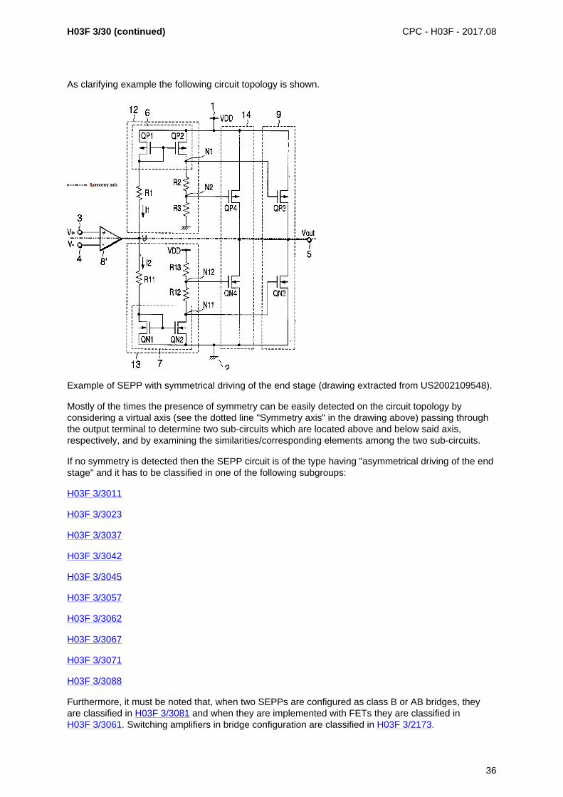
Furthermore, in the following subgroups the expression "symmetrical driving of the end stage" ispresent:
H03F 3/3016
H03F 3/3028
H03F 3/305
H03F 3/3059
H03F 3/3064
H03F 3/3076
From a circuital topology point of view, it relates to the presence of symmetry in the driving stagecircuitry of the SEPP, i.e. if the driving signal path for one of the output transistor has the same/corresponding/complementary elements of the driving signal path of the other output transistor.
35
H03F 3/30 (continued) CPC - H03F - 2017.08
As clarifying example the following circuit topology is shown.
Example of SEPP with symmetrical driving of the end stage (drawing extracted from US2002109548).
Mostly of the times the presence of symmetry can be easily detected on the circuit topology byconsidering a virtual axis (see the dotted line "Symmetry axis" in the drawing above) passing throughthe output terminal to determine two sub-circuits which are located above and below said axis,respectively, and by examining the similarities/corresponding elements among the two sub-circuits.
If no symmetry is detected then the SEPP circuit is of the type having "asymmetrical driving of the endstage" and it has to be classified in one of the following subgroups:
H03F 3/3011
H03F 3/3023
H03F 3/3037
H03F 3/3042
H03F 3/3045
H03F 3/3057
H03F 3/3062
H03F 3/3067
H03F 3/3071
H03F 3/3088
Furthermore, it must be noted that, when two SEPPs are configured as class B or AB bridges, theyare classified in H03F 3/3081 and when they are implemented with FETs they are classified inH03F 3/3061. Switching amplifiers in bridge configuration are classified in H03F 3/2173.
36
H03F 3/30 (continued) CPC - H03F - 2017.08
Indexing Code orthogonal classification
In addition to one or more EC symbols relating to the invention information, whereappropriate, one or more Indexing Code symbols relating to orthogonal classification(H03F 2203/30003 - H03F 2203/30156), i.e. covering aspects which are spanning over one or moreEC subgroups, should be allocated for this subgroup.
H03F 3/34
Dc amplifiers in which all stages are dc-coupled (H03F 3/45 takes precedence)
Definition statement
This place covers:
DC amplifiers which are formed by IC blocks, semiconductors or tubes, in which all the amplifyingstages are DC coupled, e.g. without using capacitive or switching elements, which are not specific forRF amplifiers or audio amplifiers and which have circuit topologies that are not related to other H03Fclassification symbols.
References
Limiting references
This place does not cover:
Differential amplifiers H03F 3/45
References out of a residual place
Examples of places in relation to which this place is residual:
Low frequency amplifiers H03F 3/181
High frequency amplifiers H03F 3/189
Power amplifiers H03F 3/20
Informative references
Attention is drawn to the following places, which may be of interest for search:
DC current or voltage control circuits G05F 3/02
H03F 3/38
Dc amplifiers with modulator at input and demodulator at output; Modulatorsor demodulators specially adapted for use in such amplifiers ({switchedcapacitor amplifiers H03F 3/005}; modulators in general H03C; demodulators ingeneral H03D; amplitude modulation of pulses in general H03K 7/02; amplitudedemodulation of pulses in general H03K 9/02)
Definition statement
This place covers:
DC amplifiers wherein only the AC signal is passed through the amplifying units, the DC signal isdecoupled via switching elements, e.g. see the Chopper amplifier configuration in the "Glossary ofterms" section above.
37
H03F 3/38 (continued) CPC - H03F - 2017.08
References
Application-oriented references
Examples of places where the subject matter of this place is covered when specially adapted, used fora particular purpose, or incorporated in a larger system:
Switched capacitor amplifiers H03F 3/005
Switching amplifiers H03F 3/217
Differential amplifiers H03F 3/45
Arrangements for measuring bio-electric currents or voltages A61B 5/04
Arrangements for measuring currents or voltages or for indicatingpresence or sign thereof by using conversion of dc into ac
G01R 19/18
Informative references
Attention is drawn to the following places, which may be of interest for search:
Modifications of amplifiers to reduce influence of noise generated byamplifying elements
H03F 1/26
Modulation H03C
Demodulation H03D
Switched capacitor networks H03H 19/004
Amplitude modulation of pulses in general H03K 7/02
Amplitude demodulation of pulses in general H03K 9/02
H03F 3/42
Amplifiers with two or more amplifying elements having their dc paths in serieswith the load, the control electrode of each element being excited by at leastpart of the input signal, e.g. so-called totem-pole amplifiers
Definition statement
This place covers:
In most cases totem-pole amplifiers, see the "Glossary of terms" section above, which areimplemented via semiconductor elements or tubes.
H03F 3/45
Differential amplifiers (differential sense amplifiers G11C 7/062)
Definition statement
This place covers:
Differential amplifiers in general and characterised by the technology used, the circuit topologies, andthe way that the common mode signals are rejected.
38
H03F 3/45 (continued) CPC - H03F - 2017.08
References
Limiting references
This place does not cover:
Measuring currents or voltages from sources with high internal resistanceby means of measuring circuits with high input impedance, e.g. OP-amplifiers
G01R 19/0023
Operational amplifiers for addition or subtraction in analog calculators G06G 7/14
Differential sense amplifiers G11C 7/062
Logic comparators H03K 5/24
Optical receivers with offset control of the differential preamplifier H04B 10/6933
Differential drivers H04L 25/0272
Informative references
Attention is drawn to the following places, which may be of interest for search:
Gain control in emitter coupled or cascode amplifiers H03G 1/0023
Tuned filters, switched capacitor networks H03H 7/12, H03H 19/004
Special rules of classification
Pseudo differential amplifiers (see the "Glossary of terms" section above) are usually classified inH03F 3/4508, H03F 3/45179, H03F 3/45278, H03F 3/45376.
Furthermore, it is common practice at EPO, when classifying semiconductor differential amplifiers, toconsider first the technology of the amplifying transistors and the circuit topology information, in orderto classify under one of the subgroups belonging to H03F 3/45076.
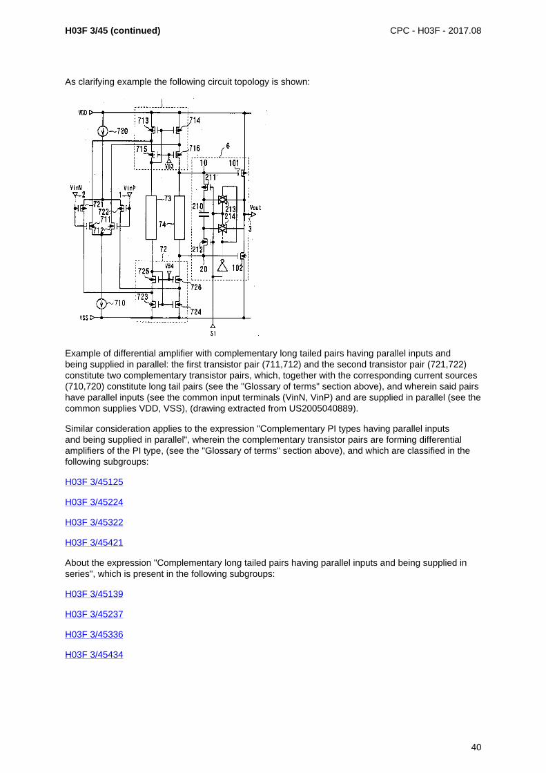
About circuit topology, the expression "Complementary long tailed pairs having parallel inputs andbeing supplied in parallel" is present in the following subgroups:
H03F 3/45112
H03F 3/4521
H03F 3/45309
H03F 3/45408
39
H03F 3/45 (continued) CPC - H03F - 2017.08
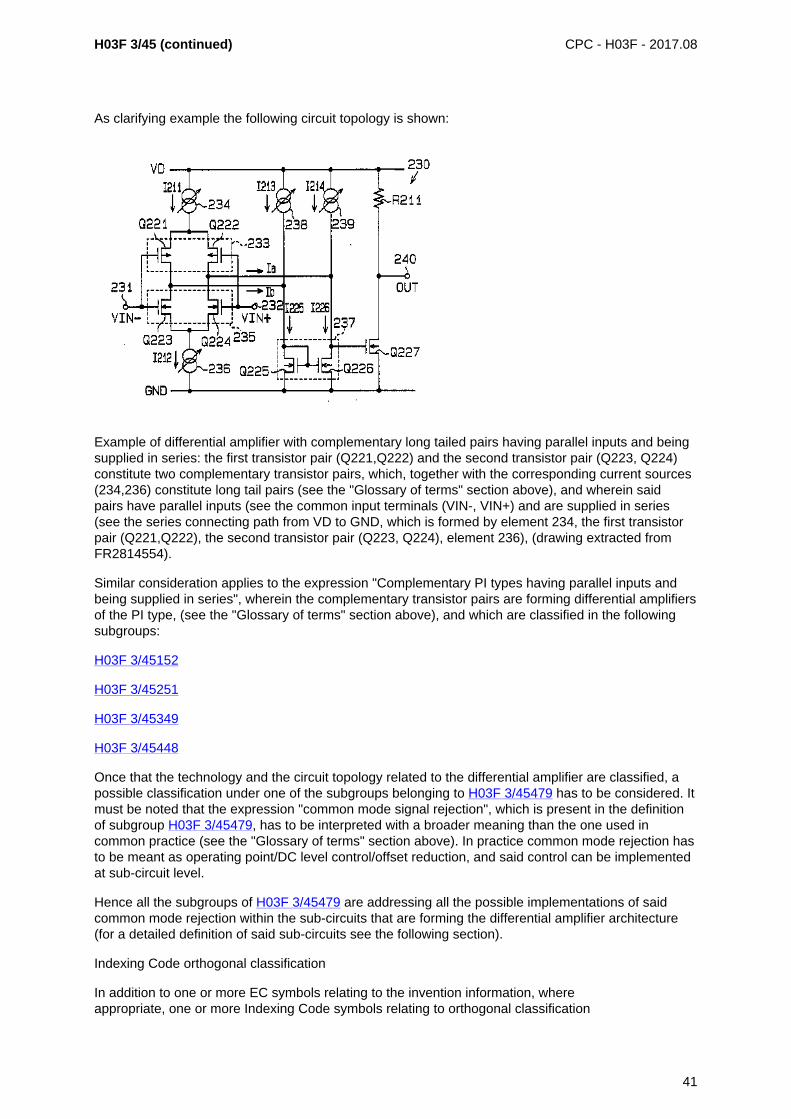
As clarifying example the following circuit topology is shown:
Example of differential amplifier with complementary long tailed pairs having parallel inputs andbeing supplied in parallel: the first transistor pair (711,712) and the second transistor pair (721,722)constitute two complementary transistor pairs, which, together with the corresponding current sources(710,720) constitute long tail pairs (see the "Glossary of terms" section above), and wherein said pairshave parallel inputs (see the common input terminals (VinN, VinP) and are supplied in parallel (see thecommon supplies VDD, VSS), (drawing extracted from US2005040889).
Similar consideration applies to the expression "Complementary PI types having parallel inputsand being supplied in parallel", wherein the complementary transistor pairs are forming differentialamplifiers of the PI type, (see the "Glossary of terms" section above), and which are classified in thefollowing subgroups:
H03F 3/45125
H03F 3/45224
H03F 3/45322
H03F 3/45421
About the expression "Complementary long tailed pairs having parallel inputs and being supplied inseries", which is present in the following subgroups:
H03F 3/45139
H03F 3/45237
H03F 3/45336
H03F 3/45434
40
H03F 3/45 (continued) CPC - H03F - 2017.08
As clarifying example the following circuit topology is shown:
Example of differential amplifier with complementary long tailed pairs having parallel inputs and beingsupplied in series: the first transistor pair (Q221,Q222) and the second transistor pair (Q223, Q224)constitute two complementary transistor pairs, which, together with the corresponding current sources(234,236) constitute long tail pairs (see the "Glossary of terms" section above), and wherein saidpairs have parallel inputs (see the common input terminals (VIN-, VIN+) and are supplied in series(see the series connecting path from VD to GND, which is formed by element 234, the first transistorpair (Q221,Q222), the second transistor pair (Q223, Q224), element 236), (drawing extracted fromFR2814554).
Similar consideration applies to the expression "Complementary PI types having parallel inputs andbeing supplied in series", wherein the complementary transistor pairs are forming differential amplifiersof the PI type, (see the "Glossary of terms" section above), and which are classified in the followingsubgroups:
H03F 3/45152
H03F 3/45251
H03F 3/45349
H03F 3/45448
Once that the technology and the circuit topology related to the differential amplifier are classified, apossible classification under one of the subgroups belonging to H03F 3/45479 has to be considered. Itmust be noted that the expression "common mode signal rejection", which is present in the definitionof subgroup H03F 3/45479, has to be interpreted with a broader meaning than the one used incommon practice (see the "Glossary of terms" section above). In practice common mode rejection hasto be meant as operating point/DC level control/offset reduction, and said control can be implementedat sub-circuit level.
Hence all the subgroups of H03F 3/45479 are addressing all the possible implementations of saidcommon mode rejection within the sub-circuits that are forming the differential amplifier architecture(for a detailed definition of said sub-circuits see the following section).
Indexing Code orthogonal classification
In addition to one or more EC symbols relating to the invention information, whereappropriate, one or more Indexing Code symbols relating to orthogonal classification
41
H03F 3/45 (continued) CPC - H03F - 2017.08
(H03F 2203/45002 - H03F 2203/45732), i.e. covering aspects which are spanning over one or moreEC subgroups, should be allocated for this subgroup.
Said aspects are mainly based on the following sub-circuits, which can be determined in a long tailedpair, PI type, and, although with limitations, in special types of differential amplifiers, e.g. pseudo-differential amplifier:
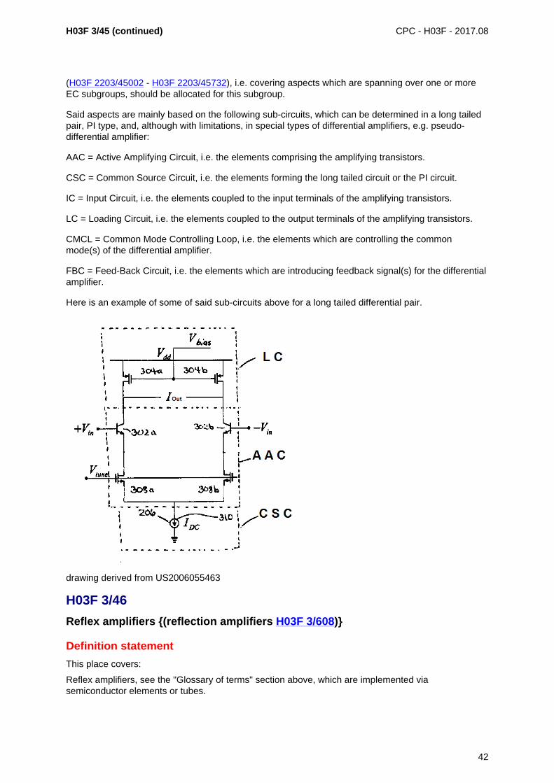
AAC = Active Amplifying Circuit, i.e. the elements comprising the amplifying transistors.
CSC = Common Source Circuit, i.e. the elements forming the long tailed circuit or the PI circuit.
IC = Input Circuit, i.e. the elements coupled to the input terminals of the amplifying transistors.
LC = Loading Circuit, i.e. the elements coupled to the output terminals of the amplifying transistors.
CMCL = Common Mode Controlling Loop, i.e. the elements which are controlling the commonmode(s) of the differential amplifier.
FBC = Feed-Back Circuit, i.e. the elements which are introducing feedback signal(s) for the differentialamplifier.
Here is an example of some of said sub-circuits above for a long tailed differential pair.
drawing derived from US2006055463
H03F 3/46
Reflex amplifiers {(reflection amplifiers H03F 3/608)}
Definition statement
This place covers:
Reflex amplifiers, see the "Glossary of terms" section above, which are implemented viasemiconductor elements or tubes.
42
H03F 3/46 (continued) CPC - H03F - 2017.08
References
Limiting references
This place does not cover:
Reflection amplifiers H03F 3/608
Application-oriented references
Examples of places where the subject matter of this place is covered when specially adapted, used fora particular purpose, or incorporated in a larger system:
Receivers comprising at least one semiconductor device having three ormore electrodes
H04B 1/24
H03F 3/50
Amplifiers in which input is applied to, or output is derived from, an impedancecommon to input and output circuits of the amplifying element, e.g. cathodefollower
Definition statement
This place covers:
Amplifiers in cathode follower, source follower, emitter follower configuration (see the "Glossary ofterms" section above).
References
Application-oriented references
Examples of places where the subject matter of this place is covered when specially adapted, used fora particular purpose, or incorporated in a larger system:
Delay circuits H03K 5/13
Special rules of classification
Indexing Code deep-indexing classification
In addition to one or more classification symbols relating to the invention information, whereappropriate, one or more Indexing Code symbols relating to deep-indexing classification(H03F 2203/5003 - H03F 2203/5045), i.e. covering embodiment aspects, should be allocated for thissubgroup.
H03F 3/54
Amplifiers using transit-time effect in tubes or semiconductor devices(parametric amplifiers H03F 7/00; solid state travelling-wave devicesH01L 45/02)
Definition statement
This place covers:
Amplifiers using transit-time effects, mostly Klystrons or Travelling Wave Tubes (TWT) see the"Glossary of terms" section above.
43
H03F 3/54 (continued) CPC - H03F - 2017.08
References
Application-oriented references
Examples of places where the subject matter of this place is covered when specially adapted, used fora particular purpose, or incorporated in a larger system:
Solid state travelling-wave devices H01L 45/02
Informative references
Attention is drawn to the following places, which may be of interest for search:
Parametric amplifiers H03F 7/00
Travelling wave tubes in general H01J 25/34
Resonators of the waveguide type H01P 7/00
H03F 3/60
Amplifiers in which coupling networks have distributed constants, e.g. withwaveguide resonators (H03F 3/54 takes precedence)
Definition statement
This place covers:
Amplifiers having distributed coupling networks, e.g. transmission lines, the so called microwaveamplifiers.
References
Limiting references
This place does not cover:
Amplifiers using transit-time effect, e.g. TWTA H03F 3/54
Parametric amplifiers H03F 7/00
Application-oriented references
Examples of places where the subject matter of this place is covered when specially adapted, used fora particular purpose, or incorporated in a larger system:
Class E amplifiers H03F 3/2176
Reflex amplifiers H03F 3/46
Multi-channel amplifiers H03F 3/68
Aerials or aerial systems providing at least two radiating patterns, beam-forming means
H01Q 25/00, H01Q 3/40
Informative references
Attention is drawn to the following places, which may be of interest for search:
Modification of amplifiers by use of distributed coupling, i.e. distributedlumped elements
H03F 1/18
Amplifiers having more than three electrodes with field-effect devices H03F 3/16
44
H03F 3/60 (continued) CPC - H03F - 2017.08
High frequency amplifiers H03F 3/189
High frequency adaptations of semiconductors H01L 23/66
Coupling devices of the waveguide type H01P 5/00
H03F 3/62
Two-way amplifiers
Definition statement
This place covers:
Two-way amplifiers, which are implemented via semiconductor elements or tubes and which aretypically employed to amplify the signal levels of forward and reverse signals.
References
Informative references
Attention is drawn to the following places, which may be of interest for search:
Multiport networks H03H 7/48
Hybrid arrangements for transceivers H04B 1/58
Intermediate station arrangements for frequency-division multiplexsystems
H04J 1/10, H04J 1/10
H03F 3/66
Amplifiers simultaneously generating oscillations of one frequency andamplifying signals of another frequency
Definition statement
This place covers:
Amplifying-mixing devices for achieving a special technical effect, e.g. interference reduction.
References
Informative references
Attention is drawn to the following places, which may be of interest for search:
Modifications of amplifiers to reduce non-linear distortion H03F 1/32
Transference of modulation from one carrier to another H03D 7/00
45
CPC - H03F - 2017.08
H03F 3/68
Combinations of amplifiers, e.g. multi-channel amplifiers for stereophonics{(power amplifiers using a combination of several semiconductor amplifiersH03F 3/211; combinations of amplifiers using coupling networks withdistributed constants H03F 3/602)}
Definition statement
This place covers:
Stereo amplifiers or multi-channel amplifiers in the low frequency range.
Multi-band amplifiers in the high frequency range, wherein multiple outputs are present.
References
Limiting references
This place does not cover:
Aerials, beam-forming means H01Q 25/00, H01Q 3/40
Circuits for stereophonic arrangements H04R 5/04
Informative references
Attention is drawn to the following places, which may be of interest for search:
Low frequency amplifiers H03F 3/181
Power amplifiers using a combination of several semiconductor amplifiers H03F 3/211
Switching amplifiers H03F 3/217
Combinations of amplifiers using coupling networks with distributedconstants
H03F 3/602
H03F 3/70
Charge amplifiers
Definition statement
This place covers:
Charge amplifiers, see the "Glossary of terms" section above.
References
Limiting references
This place does not cover:
Charge pumps for DC/DC power converters H02M 3/07
Charge pumps for automatic control of frequency or phase circuits H03L 7/0891
46
H03F 3/70 (continued) CPC - H03F - 2017.08
Application-oriented references
Examples of places where the subject matter of this place is covered when specially adapted, used fora particular purpose, or incorporated in a larger system:
Measuring acceleration by piezo-electric pick-up G01P 15/09
Integrators using operational amplifier and capacitor and resistor in thefeedback loop
G06G 7/186
Sense amplifiers G11C 7/06
H03F 3/72
Gated amplifiers, i.e. amplifiers which are rendered operative or inoperative bymeans of a control signal
Definition statement
This place covers:
Amplifiers which are enabled or disabled by means of a control signal, e.g. via a controlled switch.
References
Informative references
Attention is drawn to the following places, which may be of interest for search:
Gain control in amplifiers H03G 3/00
Electronic switching or gating H03K 17/00
Special rules of classification
Indexing Code deep-indexing classification
In addition to one or more classification symbols relating to the invention information, whereappropriate, one or more Indexing Code symbols relating to deep-indexing classification(H03F 2203/7203 - H03F 2203/7239), i.e. covering embodiment aspects, should be allocated for thissubgroup.
H03F 7/00
Parametric amplifiers ({H03F 19/00 takes precedence}; devices orarrangements for the parametric generation or amplification of light, infra-redor ultra-violet waves G02F 1/39)
Definition statement
This place covers:
Parametric amplifiers, i.e., wherein a component parameter such as capacitance or inductance isvaried to achieve amplification. .
47
CPC - H03F - 2017.08
H03F 7/02
using variable-inductance element; using variable-permeability element
Definition statement
This place covers:
Parametric amplifiers where inductance/permeability is varied to achieve amplification.
H03F 7/04
using variable-capacitance element; using variable-permittivity element
Definition statement
This place covers:
Parametric amplifiers where capacitance/permittivity is varied to achieve amplification.
H03F 9/00
Magnetic amplifiers
Definition statement
This place covers:
Amplifiers using saturable reactors as amplifying elements (aka mag-amps).
H03F 9/02
current-controlled, i.e. the load current flowing in both directions through amain coil
Definition statement
This place covers:
Magnetic amplifiers where an AC load current flows in a main coil, controlled by the current in a controlcoil.
H03F 9/04
voltage-controlled, i.e. the load current flowing in only one direction through amain coil, e.g. Logan circuits (H03F 9/06 takes precedence)
Definition statement
This place covers:
Magnetic amplifiers where a load current flows in one direction in a main coil, and typically in the otherdirection in another main coil, controlled by the current in a control coil, e.g., a control coil in a centerleg of a transformer controlling two main coils in two outer legs.
48
CPC - H03F - 2017.08
H03F 9/06
Control by voltage time integral, i.e. the load current flowing in only onedirection through a main coil, whereby the main coil winding also can be usedas a control winding, e.g. Ramey circuits
Definition statement
This place covers:
Magnetic amplifiers where the load current is auto-commutated by the main coil, the core beingperiodically reset by a control coil.
H03F 11/00
Dielectric amplifiers
Definition statement
This place covers:
Amplifiers using non-linear (hysteretic) dielectric elements to achieve amplification.
H03F 13/00
Amplifiers using amplifying element consisting of two mechanically- oracoustically-coupled transducers, e.g. telephone-microphone amplifier
Definition statement
This place covers:
Amplifiers with intermediate mechanical or acoustic energy transfer .
H03F 15/00
Amplifiers using galvano-magnetic effects not involving mechanicalmovement, e.g. using Hall effect
Definition statement
This place covers:
Amplifiers relying on galvano-magnetic effects, i.e., which arise when a conductor or semiconductorplaced in a magnetic field carries current, such as the Hall-effect.
H03F 17/00
Amplifiers using electroluminescent element or photocell
Definition statement
This place covers:
Amplifiers relying on intermediate transformation into light to achieve amplification.
49
H03F 17/00 (continued) CPC - H03F - 2017.08
References
Limiting references
This place does not cover:
Amplifiers controlled by light, e.g., for fiber optic links H03F 3/08
Amplifiers with optical coupling between stages H03F 3/085
H03F 21/00
{Amplifiers not covered by groups H03F 3/00 - H03F 19/00 (dynamo-electricamplifiers H02K)}
Definition statement
This place covers:
Amplifiers not covered elsewhere, e.g., relying on radioactivity, or using esoteric semiconductorstructures.
50


![Natural Rubber and Reclaimed Rubber Composites – A ... · Common coupling agents are silanes, isocynanates, maleated polymers and titanate-based compounds [30]. An ideal coupling](https://img.pdfslide.us/doc/110x75/5f0843a27e708231d42125ff/natural-rubber-and-reclaimed-rubber-composites-a-a-common-coupling-agents.jpg)


![The Parani-SD1100 - kanda.com · PDF fileThe Parani-SD1100 has an extension option so that users ... DAT-G01R - DAT5-G01R 300 meters DAT5-G01R - DAT5-G01R 400 meters [Antennas] SAT-G01R](https://img.pdfslide.us/doc/110x75/5a7229997f8b9a98538d6583/the-parani-sd1100-kandacom-nbsppdf-filethe-parani-sd1100-has-an.jpg)


![Bluetooth Serial Adapter, SD1000 - Lemos InternationalDAT-G01R - DAT5-G01R 300 meters DAT5-G01R - DAT5-G01R 400 meters [Antennas] SAT-G01R: +1dBi Stub Antenna DAT-G01R: +3dBi Dipole](https://img.pdfslide.us/doc/110x75/6116036f2f7ac33c53401077/bluetooth-serial-adapter-sd1000-lemos-international-dat-g01r-dat5-g01r-300.jpg)