Embed Size (px)
Citation preview
Application ReportSLOA035D–September 1999–Revised May 2015
Amplifiers and Bits: An Introduction to SelectingAmplifiers for Data Converters
Bruce Carter, Patrick Rowland, Jim Karki, Perry Miller................................ High Performance Linear Products
ABSTRACTThis application report discusses various considerations that must be taken into account when interfacinggeneral-purpose amplifiers and analog-to-digital converters. The report discusses bandwidth, resolution,analog ADC input drive, and power supply considerations for both parts.
Contents1 Introduction ................................................................................................................... 32 The Importance of Buffering................................................................................................ 33 Bandwidth..................................................................................................................... 4
3.1 Feedback Theory ................................................................................................... 43.2 Closed Loop Bandwidth............................................................................................ 53.3 Gain Bandwidth Safety Margin.................................................................................... 73.4 Gain Bandwidth Dependence on Supply Voltage .............................................................. 8
4 Slew Rate ..................................................................................................................... 95 Noise and Bits................................................................................................................ 9
5.1 Noise From the Graph ............................................................................................ 105.2 Noise From the nV or μV/√Hz Specification ................................................................... 105.3 Total Harmonic Distortion Plus Noise .......................................................................... 115.4 Signal to Noise Ratio ............................................................................................. 115.5 SINAD............................................................................................................... 125.6 Effective Number of Bits (ENOB) ............................................................................... 135.7 ADC Bits............................................................................................................ 135.8 ADC Input .......................................................................................................... 145.9 Drive Current....................................................................................................... 155.10 Slew Rate – Revisited ............................................................................................ 165.11 Settling Time ....................................................................................................... 165.12 Signal Bias ......................................................................................................... 175.13 Input Offsets ....................................................................................................... 18
6 Power Supply ............................................................................................................... 186.1 Power and Ground Planes ....................................................................................... 186.2 Input/Output Voltage Range ..................................................................................... 18
7 Summary .................................................................................................................... 188 References .................................................................................................................. 199 Appendix A: Design Example – Cellular Telephone Base Station................................................... 20
9.1 ADC Considerations .............................................................................................. 209.2 ADC Requirements for Processing GSM Signal .............................................................. 20
List of Figures
1 Amplifier and ADC ........................................................................................................... 32 Open Loop Bode Plot of an Operational Amplifier ...................................................................... 43 Closed Loop Bode Plot ..................................................................................................... 54 Noninverting Gain Stage.................................................................................................... 5
All trademarks are the property of their respective owners.
1SLOA035D–September 1999–Revised May 2015 Amplifiers and Bits: An Introduction to Selecting Amplifiers for DataConvertersSubmit Documentation Feedback
Copyright © 1999–2015, Texas Instruments Incorporated
www.ti.com
5 Noninverting Stage With Loop Broken .................................................................................... 66 Inverting Gain Stage......................................................................................................... 67 Effect of Inverting Stage Components on Gain .......................................................................... 78 Safety Margin Limiting Bandwidth ......................................................................................... 79 Typical Gain Bandwidth Product Graph (TLV2460) ..................................................................... 810 Slew Rate ..................................................................................................................... 911 Noise Characteristic of a Typical Operational Amplifier............................................................... 1012 SNR and THD Pictorial .................................................................................................... 1213 ADC Error Sources......................................................................................................... 1414 Amplifier–ADC Interface................................................................................................... 1415 Example Base Station Application ....................................................................................... 1516 Fully Differential Input to the ADC ....................................................................................... 1517 Circuit Simplification ....................................................................................................... 1618 Settling Time Limitation.................................................................................................... 1719 Input Signal Biasing Circuits .............................................................................................. 1720 Input Offset Voltage (VIO) .................................................................................................. 1821 Example of Buffer Operational Amplifier Design ....................................................................... 21
List of Tables
1 Safety Margin vs Gain Error................................................................................................ 82 Signal to Noise Ratio vs Converter Bits ................................................................................. 113 Operational Amplifier Requirements ..................................................................................... 21
2 Amplifiers and Bits: An Introduction to Selecting Amplifiers for Data SLOA035D–September 1999–Revised May 2015Converters Submit Documentation Feedback
Copyright © 1999–2015, Texas Instruments Incorporated
A/DDigitalSystem
Amplifier
Sensor or OtherAnalog Input
www.ti.com Introduction
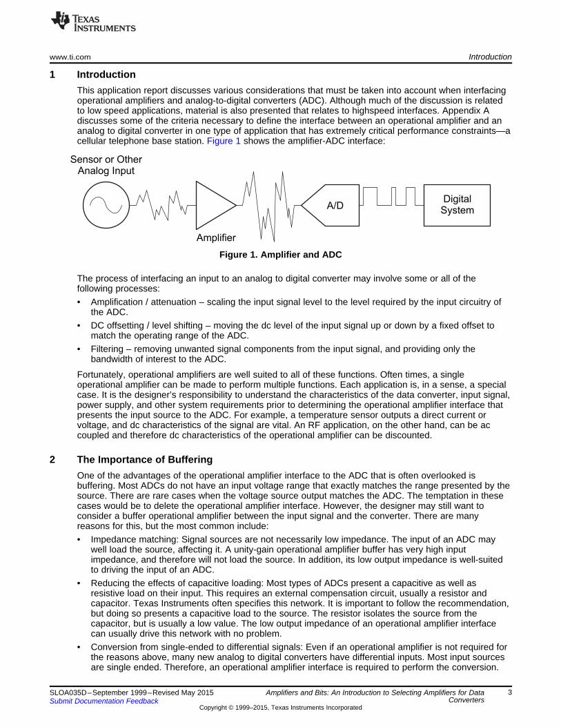
1 IntroductionThis application report discusses various considerations that must be taken into account when interfacingoperational amplifiers and analog-to-digital converters (ADC). Although much of the discussion is relatedto low speed applications, material is also presented that relates to highspeed interfaces. Appendix Adiscusses some of the criteria necessary to define the interface between an operational amplifier and ananalog to digital converter in one type of application that has extremely critical performance constraints—acellular telephone base station. Figure 1 shows the amplifier-ADC interface:
Figure 1. Amplifier and ADC
The process of interfacing an input to an analog to digital converter may involve some or all of thefollowing processes:• Amplification / attenuation – scaling the input signal level to the level required by the input circuitry of
the ADC.• DC offsetting / level shifting – moving the dc level of the input signal up or down by a fixed offset to
match the operating range of the ADC.• Filtering – removing unwanted signal components from the input signal, and providing only the
bandwidth of interest to the ADC.
Fortunately, operational amplifiers are well suited to all of these functions. Often times, a singleoperational amplifier can be made to perform multiple functions. Each application is, in a sense, a specialcase. It is the designer’s responsibility to understand the characteristics of the data converter, input signal,power supply, and other system requirements prior to determining the operational amplifier interface thatpresents the input source to the ADC. For example, a temperature sensor outputs a direct current orvoltage, and dc characteristics of the signal are vital. An RF application, on the other hand, can be accoupled and therefore dc characteristics of the operational amplifier can be discounted.
2 The Importance of BufferingOne of the advantages of the operational amplifier interface to the ADC that is often overlooked isbuffering. Most ADCs do not have an input voltage range that exactly matches the range presented by thesource. There are rare cases when the voltage source output matches the ADC. The temptation in thesecases would be to delete the operational amplifier interface. However, the designer may still want toconsider a buffer operational amplifier between the input signal and the converter. There are manyreasons for this, but the most common include:• Impedance matching: Signal sources are not necessarily low impedance. The input of an ADC may
well load the source, affecting it. A unity-gain operational amplifier buffer has very high inputimpedance, and therefore will not load the source. In addition, its low output impedance is well-suitedto driving the input of an ADC.
• Reducing the effects of capacitive loading: Most types of ADCs present a capacitive as well asresistive load on their input. This requires an external compensation circuit, usually a resistor andcapacitor. Texas Instruments often specifies this network. It is important to follow the recommendation,but doing so presents a capacitive load to the source. The resistor isolates the source from thecapacitor, but is usually a low value. The low output impedance of an operational amplifier interfacecan usually drive this network with no problem.
• Conversion from single-ended to differential signals: Even if an operational amplifier is not required forthe reasons above, many new analog to digital converters have differential inputs. Most input sourcesare single ended. Therefore, an operational amplifier interface is required to perform the conversion.
3SLOA035D–September 1999–Revised May 2015 Amplifiers and Bits: An Introduction to Selecting Amplifiers for DataConvertersSubmit Documentation Feedback
Copyright © 1999–2015, Texas Instruments Incorporated
O
I
V A
V 1 A=
+ b
Open Loop Gain: A
Gain
(dB
)
100
60
40
20
0
1 10 100 1k 10k 100k 1M
Frequency (Hz)
80
120
Bandwidth www.ti.com
This conversion can be accomplished with single-ended operational amplifiers, but is more readilyaccomplished by use of a fully differential operational amplifier.
3 BandwidthChoosing an ADC that meets the system requirements for bandwidth is the first priority. Otherconsiderations such as power or interface also come into play, but once the bandwidth of the ADC hasbeen determined, an amplifier can be chosen to go with it. Applications observe Nyquist and sample atgreater than twice the highest frequency of interest to avoid aliasing. If the Nyquist limit were the onlyimportant factor, then this discussion could stop here. Unfortunately, the question of how much bandwidthis enough? is far more complicated.
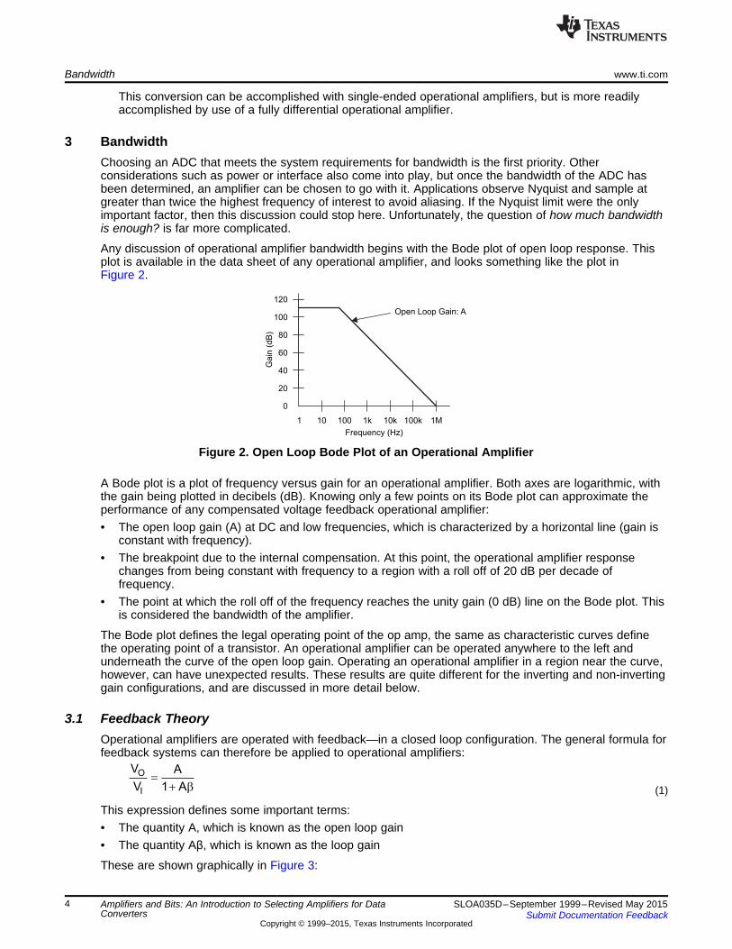
Any discussion of operational amplifier bandwidth begins with the Bode plot of open loop response. Thisplot is available in the data sheet of any operational amplifier, and looks something like the plot inFigure 2.
Figure 2. Open Loop Bode Plot of an Operational Amplifier
A Bode plot is a plot of frequency versus gain for an operational amplifier. Both axes are logarithmic, withthe gain being plotted in decibels (dB). Knowing only a few points on its Bode plot can approximate theperformance of any compensated voltage feedback operational amplifier:• The open loop gain (A) at DC and low frequencies, which is characterized by a horizontal line (gain is
constant with frequency).• The breakpoint due to the internal compensation. At this point, the operational amplifier response
changes from being constant with frequency to a region with a roll off of 20 dB per decade offrequency.
• The point at which the roll off of the frequency reaches the unity gain (0 dB) line on the Bode plot. Thisis considered the bandwidth of the amplifier.
The Bode plot defines the legal operating point of the op amp, the same as characteristic curves definethe operating point of a transistor. An operational amplifier can be operated anywhere to the left andunderneath the curve of the open loop gain. Operating an operational amplifier in a region near the curve,however, can have unexpected results. These results are quite different for the inverting and non-invertinggain configurations, and are discussed in more detail below.
3.1 Feedback TheoryOperational amplifiers are operated with feedback—in a closed loop configuration. The general formula forfeedback systems can therefore be applied to operational amplifiers:
(1)
This expression defines some important terms:• The quantity A, which is known as the open loop gain• The quantity Aβ, which is known as the loop gain
These are shown graphically in Figure 3:
4 Amplifiers and Bits: An Introduction to Selecting Amplifiers for Data SLOA035D–September 1999–Revised May 2015Converters Submit Documentation Feedback
Copyright © 1999–2015, Texas Instruments Incorporated
O O F
GI I G
G F
V V RAIf A desired closed loop gain, 1
A RV V R1
R R
= >> = +
´
+
+
Open Loop Gain: A
Gain
(dB
)
100
60
40
20
0
1 10 100 1k 10k 100k 1M
Frequency (Hz)
80
120
AClosed Loop Gain:
1 A+ b
1+Aβ
www.ti.com Bandwidth
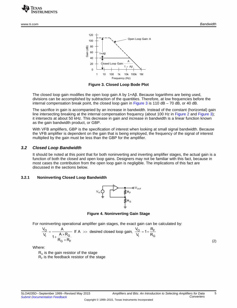
Figure 3. Closed Loop Bode Plot
The closed loop gain modifies the open loop gain A by 1+Aβ. Because logarithms are being used,divisions can be accomplished by subtraction of the quantities. Therefore, at low frequencies before theinternal compensation break point, the closed loop gain in Figure 3 is 110 dB – 70 dB, or 40 dB.
The sacrifice in gain is accompanied by an increase in bandwidth. Instead of the constant (horizontal) gainline intersecting breaking at the internal compensation frequency (about 100 Hz in Figure 2 and Figure 3);it intersects at about 50 kHz. This decrease in gain and increase in bandwidth is a linear function knownas the gain bandwidth product, or GBP.
With VFB amplifiers, GBP is the specification of interest when looking at small signal bandwidth. Becausethe VFB amplifier is dependent on the gain that is being employed, the frequency of the signal of interestmultiplied by the gain must be less than the GBP for the amplifier.
3.2 Closed Loop BandwidthIt should be noted at this point that for both noninverting and inverting amplifier stages, the actual gain is afunction of both the closed and open loop gains. Designers may not be familiar with this fact, because inmost cases the contribution from the open loop gain is negligible. The implications of this fact arediscussed in the sections below.
3.2.1 Noninverting Closed Loop Bandwidth
Figure 4. Noninverting Gain Stage
For noninverting operational amplifier gain stages, the exact gain can be calculated by:
(2)
Where:RG is the gain resistor of the stageRF is the feedback resistor of the stage
5SLOA035D–September 1999–Revised May 2015 Amplifiers and Bits: An Introduction to Selecting Amplifiers for DataConvertersSubmit Documentation Feedback
Copyright © 1999–2015, Texas Instruments Incorporated
F
G F
A R
R R
- ´
+
F
O G F O F
GI I G
G F
A R
V R R V RIf A desired closed loop gain,
A RV V R1
R R
- ´
+
= >> = -
´
+
+
O F
I G
V R1
V R= +
G
G F
R
R R+
Bandwidth www.ti.com
Figure 5. Noninverting Stage With Loop Broken
The quantity is the proportion of output voltage fed back the input (from the voltage divider rule).
Equation 2 defines the noninverting closed loop gain. The point at which the closed loop gain intersectsthe open loop gain curve of the operational amplifier is the closed loop bandwidth. Therefore, the gainbandwidth product (GBP) is equal to:
GBP = (noninverting closed loop gain) x (closed loop bandwidth) (3)
Designers are probably much more familiar with the expression , but should keep in mind it isan approximation based on infinite open loop gain.
3.2.2 Inverting Closed Loop Bandwidth
Figure 6. Inverting Gain Stage
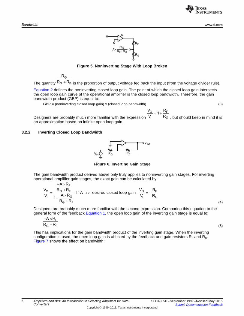
The gain bandwidth product derived above only truly applies to noninverting gain stages. For invertingoperational amplifier gain stages, the exact gain can be calculated by:
(4)
Designers are probably much more familiar with the second expression. Comparing this equation to thegeneral form of the feedback Equation 1, the open loop gain of the inverting gain stage is equal to:
(5)
This has implications for the gain bandwidth product of the inverting gain stage. When the invertingconfiguration is used, the open loop gain is affected by the feedback and gain resistors RF and RG.Figure 7 shows the effect on bandwidth:
6 Amplifiers and Bits: An Introduction to Selecting Amplifiers for Data SLOA035D–September 1999–Revised May 2015Converters Submit Documentation Feedback
Copyright © 1999–2015, Texas Instruments Incorporated
www.ti.com Bandwidth
Figure 7. Effect of Inverting Stage Components on Gain
For the unity gain stage, where RG = RF, the gain is reduced by 1/2.
This effect can be calculated visually on the open loop Bode plot. Simply draw a horizontal linecorresponding to the reduced gain to the compensation break point frequency, then draw a diagonal lineparallel to the original open loop plot down to the 0 dB axis. This is the adjusted gain plot for the op ampstage with inverting gain resistors.
Another way of expressing this is that for an inverting amplifier of gain one, half of the output signal is fedback, similar to a noninverting gain of 2.
Therefore, high-speed applications, where the speed of the interface is the dominant requirement, shoulduse the noninverting configuration. If common mode rejection, noise, and harmonic distortion are thedominant requirements, then the inverting configuration should be used.
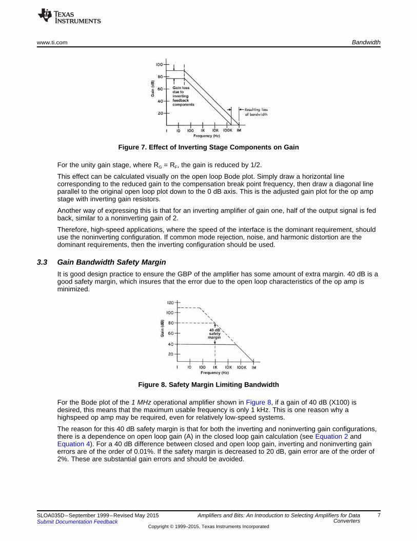
3.3 Gain Bandwidth Safety MarginIt is good design practice to ensure the GBP of the amplifier has some amount of extra margin. 40 dB is agood safety margin, which insures that the error due to the open loop characteristics of the op amp isminimized.
Figure 8. Safety Margin Limiting Bandwidth
For the Bode plot of the 1 MHz operational amplifier shown in Figure 8, if a gain of 40 dB (X100) isdesired, this means that the maximum usable frequency is only 1 kHz. This is one reason why ahighspeed op amp may be required, even for relatively low-speed systems.
The reason for this 40 dB safety margin is that for both the inverting and noninverting gain configurations,there is a dependence on open loop gain (A) in the closed loop gain calculation (see Equation 2 andEquation 4). For a 40 dB difference between closed and open loop gain, inverting and noninverting gainerrors are of the order of 0.01%. If the safety margin is decreased to 20 dB, gain error are of the order of2%. These are substantial gain errors and should be avoided.
7SLOA035D–September 1999–Revised May 2015 Amplifiers and Bits: An Introduction to Selecting Amplifiers for DataConvertersSubmit Documentation Feedback
Copyright © 1999–2015, Texas Instruments Incorporated
Bandwidth www.ti.com
If more accuracy is needed, the safety margin should be increased. Utilizing op amps with high gainbandwidth products at lower gains can do this. If accuracy is a more important consideration than noise,more than one op amp operated at a lower gain is better than a single op amp operated at high gain.Accuracy increases dramatically as the safety margin is increased. For a safety margin of 60 dB, the gainerrors are in the order of 0.0001%. Table 1 shows the effect of safety margin on gain accuracy forinverting and noninverting stages.
Table 1. Safety Margin vs Gain Error
Safety Margin (dB) Inverting Gain Error (%) Non-inverting Gain Error (%)0 66.6 5010 16.7 9.0920 1.96 0.9930 0.2 0.099940 0.02 0.0150 0.002 0.00160 0.0002 0.000170 0.00002 0.0000180 0.000002 0.00001
These figures come from Equation 2 and Equation 4. For a given safety margin, a noninverting stage haslower gain error.
There is an additional problem associated with the open loop dependence. Referring to Figure 8, there isa slight frequency dependence associated with the closed loop gain. The safety factor at 1 kHz is 40 dB,at 100 Hz the safety margin has increased to 60 dB. Therefore, there is a slight change in gain.
Most designers are unaware of the open loop effects on operational amplifier gain circuits because theyare used to designing with low gains, utilizing operational amplifiers with high gain bandwidth products.The error produced by the open loop gain of the operational amplifier is much less than the accuracy ofthe resistors used to define the closed loop gain. It is somewhat analogous to the case of special relativity.The really bizarre effects of special relativity do not show up until one is traveling very close to the speedof light. The really bizarre effects of open loop gain on closed loop gain do not show up until one isoperating with a low safety margin.
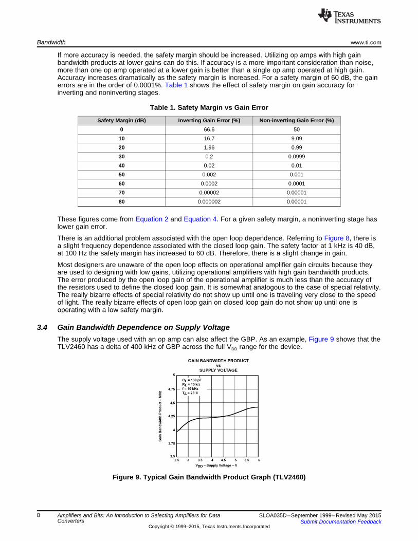
3.4 Gain Bandwidth Dependence on Supply VoltageThe supply voltage used with an op amp can also affect the GBP. As an example, Figure 9 shows that theTLV2460 has a delta of 400 kHz of GBP across the full VDD range for the device.
Figure 9. Typical Gain Bandwidth Product Graph (TLV2460)
8 Amplifiers and Bits: An Introduction to Selecting Amplifiers for Data SLOA035D–September 1999–Revised May 2015Converters Submit Documentation Feedback
Copyright © 1999–2015, Texas Instruments Incorporated
www.ti.com Slew Rate
4 Slew RateAnother specification that is of interest with respect to large signal bandwidth is slew rate (SR). Slew ratebecomes important when signal levels are large (close to the voltage rails of the operational amplifier), orsignals have a non-sinusoidal nature (square waves, pulses, triangle waves, sawtooth waves, ramps, etc.)These waveforms have harmonic content that may exceed the bandwidth of the operational amplifier.
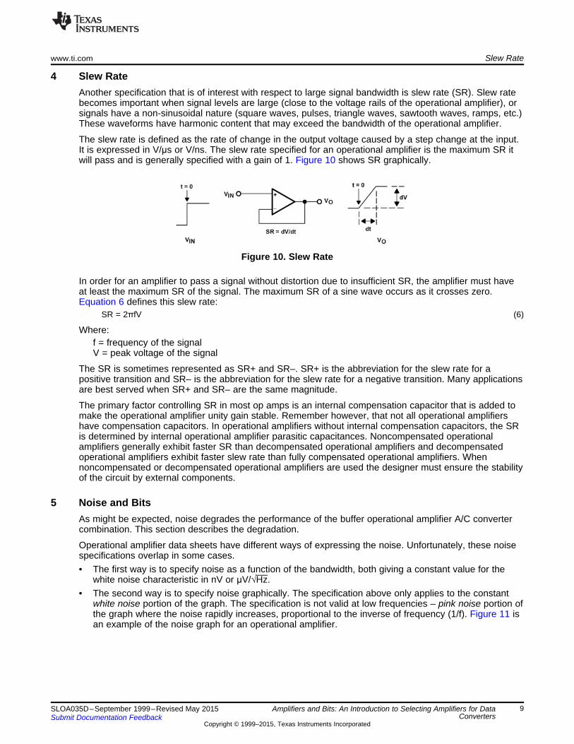
The slew rate is defined as the rate of change in the output voltage caused by a step change at the input.It is expressed in V/μs or V/ns. The slew rate specified for an operational amplifier is the maximum SR itwill pass and is generally specified with a gain of 1. Figure 10 shows SR graphically.
Figure 10. Slew Rate
In order for an amplifier to pass a signal without distortion due to insufficient SR, the amplifier must haveat least the maximum SR of the signal. The maximum SR of a sine wave occurs as it crosses zero.Equation 6 defines this slew rate:
SR = 2πfV (6)
Where:f = frequency of the signalV = peak voltage of the signal
The SR is sometimes represented as SR+ and SR–. SR+ is the abbreviation for the slew rate for apositive transition and SR– is the abbreviation for the slew rate for a negative transition. Many applicationsare best served when SR+ and SR– are the same magnitude.
The primary factor controlling SR in most op amps is an internal compensation capacitor that is added tomake the operational amplifier unity gain stable. Remember however, that not all operational amplifiershave compensation capacitors. In operational amplifiers without internal compensation capacitors, the SRis determined by internal operational amplifier parasitic capacitances. Noncompensated operationalamplifiers generally exhibit faster SR than decompensated operational amplifiers and decompensatedoperational amplifiers exhibit faster slew rate than fully compensated operational amplifiers. Whennoncompensated or decompensated operational amplifiers are used the designer must ensure the stabilityof the circuit by external components.
5 Noise and BitsAs might be expected, noise degrades the performance of the buffer operational amplifier A/C convertercombination. This section describes the degradation.
Operational amplifier data sheets have different ways of expressing the noise. Unfortunately, these noisespecifications overlap in some cases.• The first way is to specify noise as a function of the bandwidth, both giving a constant value for the
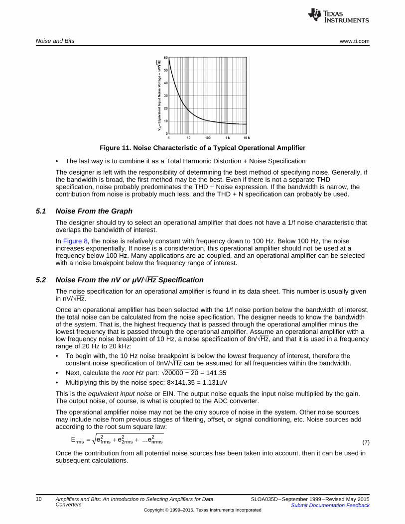
white noise characteristic in nV or μV/√Hz.• The second way is to specify noise graphically. The specification above only applies to the constant
white noise portion of the graph. The specification is not valid at low frequencies – pink noise portion ofthe graph where the noise rapidly increases, proportional to the inverse of frequency (1/f). Figure 11 isan example of the noise graph for an operational amplifier.
9SLOA035D–September 1999–Revised May 2015 Amplifiers and Bits: An Introduction to Selecting Amplifiers for DataConvertersSubmit Documentation Feedback
Copyright © 1999–2015, Texas Instruments Incorporated
2 2 2
rms 1rms 2rms nrmsE e e ...e= + +
Noise and Bits www.ti.com
Figure 11. Noise Characteristic of a Typical Operational Amplifier
• The last way is to combine it as a Total Harmonic Distortion + Noise Specification
The designer is left with the responsibility of determining the best method of specifying noise. Generally, ifthe bandwidth is broad, the first method may be the best. Even if there is not a separate THDspecification, noise probably predominates the THD + Noise expression. If the bandwidth is narrow, thecontribution from noise is probably much less, and the THD + N specification can probably be used.
5.1 Noise From the GraphThe designer should try to select an operational amplifier that does not have a 1/f noise characteristic thatoverlaps the bandwidth of interest.
In Figure 8, the noise is relatively constant with frequency down to 100 Hz. Below 100 Hz, the noiseincreases exponentially. If noise is a consideration, this operational amplifier should not be used at afrequency below 100 Hz. Many applications are ac-coupled, and an operational amplifier can be selectedwith a noise breakpoint below the frequency range of interest.
5.2 Noise From the nV or μV/√Hz SpecificationThe noise specification for an operational amplifier is found in its data sheet. This number is usually givenin nV/√Hz.
Once an operational amplifier has been selected with the 1/f noise portion below the bandwidth of interest,the total noise can be calculated from the noise specification. The designer needs to know the bandwidthof the system. That is, the highest frequency that is passed through the operational amplifier minus thelowest frequency that is passed through the operational amplifier. Assume an operational amplifier with alow frequency noise breakpoint of 10 Hz, a noise specification of 8n/√Hz, and that it is used in a frequencyrange of 20 Hz to 20 kHz:• To begin with, the 10 Hz noise breakpoint is below the lowest frequency of interest, therefore the
constant noise specification of 8nV/√Hz can be assumed for all frequencies within the bandwidth.• Next, calculate the root Hz part: √20000 − 20 = 141.35• Multiplying this by the noise spec: 8×141.35 = 1.131μV
This is the equivalent input noise or EIN. The output noise equals the input noise multiplied by the gain.The output noise, of course, is what is coupled to the ADC converter.
The operational amplifier noise may not be the only source of noise in the system. Other noise sourcesmay include noise from previous stages of filtering, offset, or signal conditioning, etc. Noise sources addaccording to the root sum square law:
(7)
Once the contribution from all potential noise sources has been taken into account, then it can be used insubsequent calculations.
10 Amplifiers and Bits: An Introduction to Selecting Amplifiers for Data SLOA035D–September 1999–Revised May 2015Converters Submit Documentation Feedback
Copyright © 1999–2015, Texas Instruments Incorporated
SNR dB 1.76n
6.02
-
=
2 2 2
rms 1rms 2rms nrmsE e e ...e= + +
( )Harmonic Voltages + Noise VoltagesTHD N 100%
Fundamental
é ù+ = ´ê ú
ê úë û
S
www.ti.com Noise and Bits
5.3 Total Harmonic Distortion Plus NoiseThe total harmonic distortion plus noise op amp parameter, THD+N, is defined as the ratio of the RMSnoise voltage plus the RMS harmonic voltage of the fundamental signal to the fundamental RMS voltagesignal at the output. It is expressed in dBc or percent (%).
The dBc is a common usage, and is a relative term with a variable reference, like dB alone. It means dBreferenced to a carrier level. For example, Spurious signals less than –50 dBc means that spurioussignals will be at least 50 dB less than some specified carrier level present (which also means 50 dB lessthan the desired signal).
THD + N compares the frequency content of the output signal to the frequency content of the input.Ideally, if the input signal is a pure sine wave, the output signal is a pure sine wave. Due to nonlinearityand noise sources within the op amp, the output is never pure.
To state another way, THD + N is the ratio of all other frequency components to the fundamental.
(8)
Typically an operational amplifier must be operated at or below its recommended operating conditions torealize low THD.
Unfortunately, if the THD is coupled with the noise in this way, the designer may have no choice but toadd the noise calculated from the nV or μV/√Hz specification to the THD+N specification. Fortunately,these two specifications are uncorrelated, and are therefore added according to the root sum squaredmethod:
(9)
5.4 Signal to Noise RatioThe title of this section is descriptive of this specification. It can be approached from the operationalamplifier side of the interface as well as the ADC converter side, and the performance of the two matched.In practice, the operational amplifier signal to noise ratio should be much better than that of the ADCconverter, to avoid limiting its performance.
Assuming that the noise level is now known, the signal level divided by the noise level, gives the signal tonoise ratio. If both are expressed in dB, the noise level can simply be subtracted from the signal level.
The ADC signal to noise ratio can also be determined in terms of the bits of the converter:SNR dB = 6.02 X n + 1.76 (10)
or
(11)
Equation 11 is a quick approximation of the number of converter bits required for the application. It is validfor sinusoidal signal signals only, and assumes 0 INL and 0 DNL error in the converter. A simple table canbe constructed for the number of data converter bits versus SNR:
Table 2. Signal to Noise Ratio vs Converter Bits
Number of Bits (n) SNR (dB)4 25.848 49.9210 61.9612 7414 86.0416 98.818 110.1220 122.16
11SLOA035D–September 1999–Revised May 2015 Amplifiers and Bits: An Introduction to Selecting Amplifiers for Data ConvertersSubmit Documentation Feedback
Copyright © 1999–2015, Texas Instruments Incorporated
Signal THD NSINAD SNR D
THD N
+ += + =
+
( )( )
All Frequency ComponentsSINAD
All Frequency Components - Fundamental Component=
S
S
Noise and Bits www.ti.com
Table 2. Signal to Noise Ratio vs Converter Bits (continued)Number of Bits (n) SNR (dB)
22 134.224 146.24
5.5 SINADOnce the Total Harmonic Distortion + Noise (THD + N) specification is known, it can be used to calculatethe SINAD. A brief introduction to the SINAD is in order.
SINAD is a figure of merit used to describe the quality of the signal. It is basically a measure of thedistortion present in an audio signal due to noise and harmonics. The general form for mathematicalexpression of SINAD is as follows:
(12)
The SINAD ratio of the modulated signal is computed by removing the fundamental signal and then byexpressing the RMS value of the remaining power spectrum in decibels relative to the RMS value of thissame power spectrum in which the fundamental signal has been removed. The ratio of the compositesignal to the noise plus distortion component is the SINAD ratio.
SINAD can also be defined as:
(13)
Hence the name SINAD (Signal to Noise And Distortion)
NOTE: These numbers are scalar and not in dB.
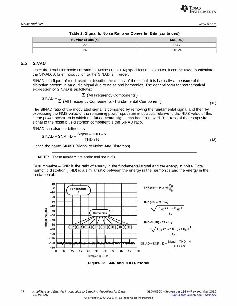
To summarize – SNR is the ratio of energy in the fundamental signal and the energy in noise. Totalharmonic distortion (THD) is a similar ratio between the energy in the harmonics and the energy in thefundamental.
Figure 12. SNR and THD Pictorial
12 Amplifiers and Bits: An Introduction to Selecting Amplifiers for Data SLOA035D–September 1999–Revised May 2015Converters Submit Documentation Feedback
Copyright © 1999–2015, Texas Instruments Incorporated
N
Vfullscale1 LSB
2 1
=
-
( )10
THD N%20log THD N dB
100
+æ ö= +ç ÷
è ø
THD N%THD N
100
+= +
( )SINAD dB 1.76ENOB
6.02
é ù-ë û=
www.ti.com Noise and Bits
5.6 Effective Number of Bits (ENOB)A given converter is advertised as having a certain number of bits, the common sizes being given in Table2 above. The converter itself has limitations that degrade its own performance. These are discussed in thenext section. The SNR and THD of the buffer op amp degrade the performance of the ADC conversionsystem, lowering the number of meaningful (effective) bits of information that it can provide to the dataprocessing elements of the system.
SINAD takes into account the harmonics and the noise energy, and thus produces a real SNR that canlead to the effective number of bits. ENOB is defined as:
(14)
Data converter specifications offer either SNR + D or THD + N in dB; thus, this equation is easy to use.Conversely, amplifier specifications usually specify SNR + D or THD + N in percent instead of dB. Thisrequires some mathematical manipulation to use the same equations.
Translating percent to dB is straightforward. For example, the following steps translate THD + N% to THD+ N dB, but the same steps can be used to translate SNR + D or SINAD from percent to dB.
(15)
Then:20 log (THD + N) = (THD + N) dB (16)
This can be put into one mathematical expression,
(17)
but it is often useful to have the intermediate step of a scalar number, because Equation 15 is also statedin scalar numbers. To use this equation in dB, remember:
logBA = A × logB and thus, Equation 13 in dB is :SINAD dB = SNR + D dB = (THD + N dB)–1 = –(THD + N) dB (18)
The ability to convert between percent and dB simplifies matching the appropriate SINAD specificationsbetween an amplifier and an ADC. Ideally, choosing an amplifier and an ADC that have the same SINADrealizes the full potential of the signal chain. In practice, choosing an amplifier that has a slightly higherSINAD ensures that it does not degrade the system performance.
For example, the TLV1572 ADC has a typical SNR+D of 58 dB that equates to an ENOB of 9.35 bits. Anamplifier like the TLV2770 is an excellent choice to drive this ADC. The TLV2770 has more than sufficientGBP (5.1 MHz typical) to place significant gain on the input signal. Also, the THD+N graphs in the back ofthe TLV2770 data sheet match the performance of the TLV1572 in nearly all cases, with the onlyexception being a relatively high supply voltage and high signal gain.
5.7 ADC BitsAn ADC specification that varies with VCC levels is the size of one least significant bit (LSB). Thisbecomes clear with Equation 19:
(19)
Where n = resolution of the ADC
For the case of a 12-bit (ENOB) ADC, moving from a 5-V to 3-V full-scale range results in a reduction insize of 1 LSB from 1.22 mV to 732 μV. For an ADC like the TLV1572 with a VCC range of 2.7 to 5.5 V, thisresults in a range of LSB size (5.37 mV to 2.64 mV). The main concern is that, particularly in moving asystem to a lower voltage, the LSB does not shrink to the point of being susceptible to system parasitics.
The ADC is not a perfect component. There are errors that affect its accuracy. These errors affect theleast significant bits and act as a limitation to ultimate system accuracy.
13SLOA035D–September 1999–Revised May 2015 Amplifiers and Bits: An Introduction to Selecting Amplifiers for DataConvertersSubmit Documentation Feedback
Copyright © 1999–2015, Texas Instruments Incorporated
Noise and Bits www.ti.com
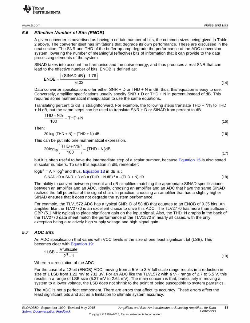
Figure 13. ADC Error Sources
These errors are of three different types:• Differential nonlinearity, where the input voltage step size is not the same for each change in output
code. It is shown in Figure 13(a).• Offset error, where all of the input voltages have to be a fixed value above or below the ideal to
produce changes in output code. It is shown in Figure 13(b).• Gain error, which means that the change in voltage to produce digital codes is below or above the
ideal gain / output code function. It is a cumulative error, shown in Figure 13(c).
These error sources are usually combined in the ADC data sheet and expressed as their sum. Thisspecification is known as the integral nonlinearity (INL) of the ADC. It is the responsibility of the designerto understand these error sources and their implications. Ideally, a data converter would have zero bits ofINL. In practice, however, the INL can be as large as 1/2 bit before the data converter has to bedowngraded in ENOB. INL larger than 1/2 bit can be tolerated only if the source of the error is offset in anac-coupled system. The designer may be forced to specify an ADC with more bits than originally thought,so that throwing away least significant bits can eliminate the INL error.
As conversion frequency increases, the ENOB will decrease. The reason is obvious—the conversionneeds to be done with less and less settling time, and therefore more unpredictability in the value of inputvoltage.
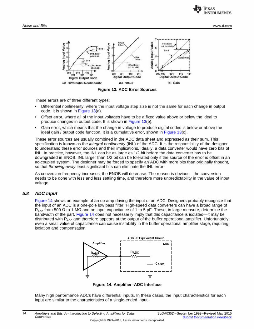
5.8 ADC InputFigure 14 shows an example of an op amp driving the input of an ADC. Designers probably recognize thatthe input of an ADC is a one-pole low pass filter. High-speed data converters can have a broad range ofRADC from 500 Ω to 1 MΩ and an input capacitance of 1 to 5 pF. These, in large measure, determine thebandwidth of the part. Figure 14 does not necessarily imply that this capacitance is isolated—it may bedistributed with RADC and therefore appears at the output of the buffer operational amplifier. Unfortunately,even a small value of capacitance can cause instability in the buffer operational amplifier stage, requiringisolation and compensation.
Figure 14. Amplifier–ADC Interface
Many high performance ADCs have differential inputs. In these cases, the input characteristics for eachinput are similar to the characteristics of a single-ended input.
14 Amplifiers and Bits: An Introduction to Selecting Amplifiers for Data SLOA035D–September 1999–Revised May 2015Converters Submit Documentation Feedback
Copyright © 1999–2015, Texas Instruments Incorporated
www.ti.com Noise and Bits
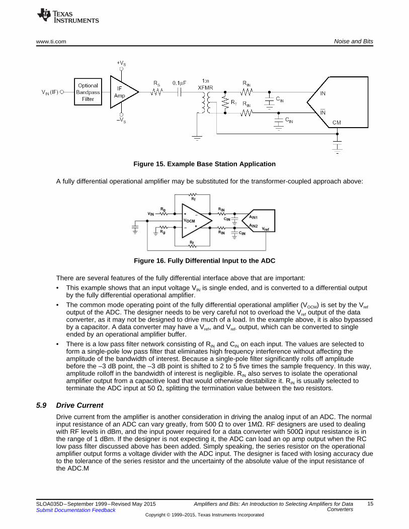
Figure 15. Example Base Station Application
A fully differential operational amplifier may be substituted for the transformer-coupled approach above:
Figure 16. Fully Differential Input to the ADC
There are several features of the fully differential interface above that are important:• This example shows that an input voltage VIN is single ended, and is converted to a differential output
by the fully differential operational amplifier.• The common mode operating point of the fully differential operational amplifier (VOCM) is set by the Vref
output of the ADC. The designer needs to be very careful not to overload the Vref output of the dataconverter, as it may not be designed to drive much of a load. In the example above, it is also bypassedby a capacitor. A data converter may have a Vref+ and Vref- output, which can be converted to singleended by an operational amplifier buffer.
• There is a low pass filter network consisting of RIN and CIN on each input. The values are selected toform a single-pole low pass filter that eliminates high frequency interference without affecting theamplitude of the bandwidth of interest. Because a single-pole filter significantly rolls off amplitudebefore the –3 dB point, the –3 dB point is shifted to 2 to 5 five times the sample frequency. In this way,amplitude rolloff in the bandwidth of interest is negligible. RIN also serves to isolate the operationalamplifier output from a capacitive load that would otherwise destabilize it. RIN is usually selected toterminate the ADC input at 50 Ω, splitting the termination value between the two resistors.
5.9 Drive CurrentDrive current from the amplifier is another consideration in driving the analog input of an ADC. The normalinput resistance of an ADC can vary greatly, from 500 Ω to over 1MΩ. RF designers are used to dealingwith RF levels in dBm, and the input power required for a data converter with 500Ω input resistance is inthe range of 1 dBm. If the designer is not expecting it, the ADC can load an op amp output when the RClow pass filter discussed above has been added. Simply speaking, the series resistor on the operationalamplifier output forms a voltage divider with the ADC input. The designer is faced with losing accuracy dueto the tolerance of the series resistor and the uncertainty of the absolute value of the input resistance ofthe ADC.M
15SLOA035D–September 1999–Revised May 2015 Amplifiers and Bits: An Introduction to Selecting Amplifiers for DataConvertersSubmit Documentation Feedback
Copyright © 1999–2015, Texas Instruments Incorporated
V(t)I Where t 0.
R= =
Noise and Bits www.ti.com
There are two ways of dealing with this problem. One is to delete the RC low pass filter completely, andlive with potential high frequency interference and the input capacitance of the ADC, which could causeoperational amplifier instability and is obviously undesirable.
The other is to use auto calibration techniques to compensate for these tolerances, throwing away a fewbits of conversion on the high and low end of the ADC conversion range. This assumes that the inputsignal is ac-coupled, and dc accuracy is not important.
5.10 Slew Rate – RevisitedWhen dealing with the ADC input itself, and the ADC used with a compensating low pass filter, there arerise time issues associated with the RC time constants involved. These show up as slew rate limitations,as discussed in the slew rate above. This discussion, however, describes the components external to theoperational amplifier that affect slew rate – the compensating low pass filter, and the ADC input. Thecapacitors affect the slew rate because the driving voltage must charge them.
This charge time is governed by the equation:V(t) = Voe-(t/RC) (20)
Where: Vo is the steady state V on the capacitor.
Assuming the input voltage at the voltage source (Vs) is steady from t = – ∞ up until t = 0, it can bedetermined that Vo = Vs. The simple explanation is that, in a dc steady state, the capacitor acts like anopen circuit, thus having the same voltage as Vs.
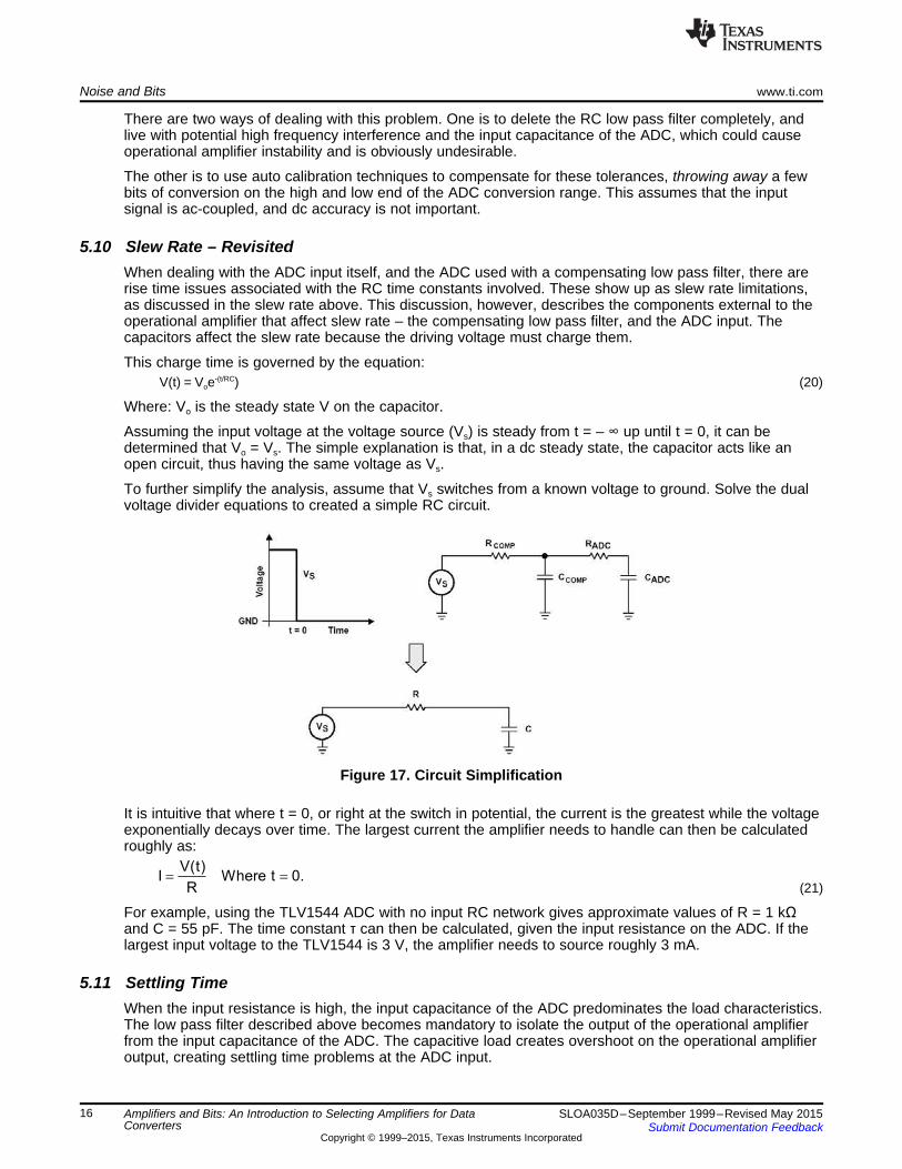
To further simplify the analysis, assume that Vs switches from a known voltage to ground. Solve the dualvoltage divider equations to created a simple RC circuit.
Figure 17. Circuit Simplification
It is intuitive that where t = 0, or right at the switch in potential, the current is the greatest while the voltageexponentially decays over time. The largest current the amplifier needs to handle can then be calculatedroughly as:
(21)
For example, using the TLV1544 ADC with no input RC network gives approximate values of R = 1 kΩand C = 55 pF. The time constant τ can then be calculated, given the input resistance on the ADC. If thelargest input voltage to the TLV1544 is 3 V, the amplifier needs to source roughly 3 mA.
5.11 Settling TimeWhen the input resistance is high, the input capacitance of the ADC predominates the load characteristics.The low pass filter described above becomes mandatory to isolate the output of the operational amplifierfrom the input capacitance of the ADC. The capacitive load creates overshoot on the operational amplifieroutput, creating settling time problems at the ADC input.
16 Amplifiers and Bits: An Introduction to Selecting Amplifiers for Data SLOA035D–September 1999–Revised May 2015Converters Submit Documentation Feedback
Copyright © 1999–2015, Texas Instruments Incorporated
www.ti.com Noise and Bits
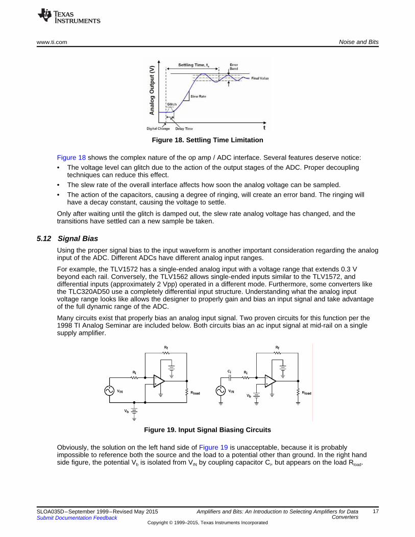
Figure 18. Settling Time Limitation
Figure 18 shows the complex nature of the op amp / ADC interface. Several features deserve notice:• The voltage level can glitch due to the action of the output stages of the ADC. Proper decoupling
techniques can reduce this effect.• The slew rate of the overall interface affects how soon the analog voltage can be sampled.• The action of the capacitors, causing a degree of ringing, will create an error band. The ringing will
have a decay constant, causing the voltage to settle.
Only after waiting until the glitch is damped out, the slew rate analog voltage has changed, and thetransitions have settled can a new sample be taken.
5.12 Signal BiasUsing the proper signal bias to the input waveform is another important consideration regarding the analoginput of the ADC. Different ADCs have different analog input ranges.
For example, the TLV1572 has a single-ended analog input with a voltage range that extends 0.3 Vbeyond each rail. Conversely, the TLV1562 allows single-ended inputs similar to the TLV1572, anddifferential inputs (approximately 2 Vpp) operated in a different mode. Furthermore, some converters likethe TLC320AD50 use a completely differential input structure. Understanding what the analog inputvoltage range looks like allows the designer to properly gain and bias an input signal and take advantageof the full dynamic range of the ADC.
Many circuits exist that properly bias an analog input signal. Two proven circuits for this function per the1998 TI Analog Seminar are included below. Both circuits bias an ac input signal at mid-rail on a singlesupply amplifier.
Figure 19. Input Signal Biasing Circuits
Obviously, the solution on the left hand side of Figure 19 is unacceptable, because it is probablyimpossible to reference both the source and the load to a potential other than ground. In the right handside figure, the potential Vb is isolated from VIN by coupling capacitor Ci, but appears on the load Rload.
17SLOA035D–September 1999–Revised May 2015 Amplifiers and Bits: An Introduction to Selecting Amplifiers for DataConvertersSubmit Documentation Feedback
Copyright © 1999–2015, Texas Instruments Incorporated
Noise and Bits www.ti.com
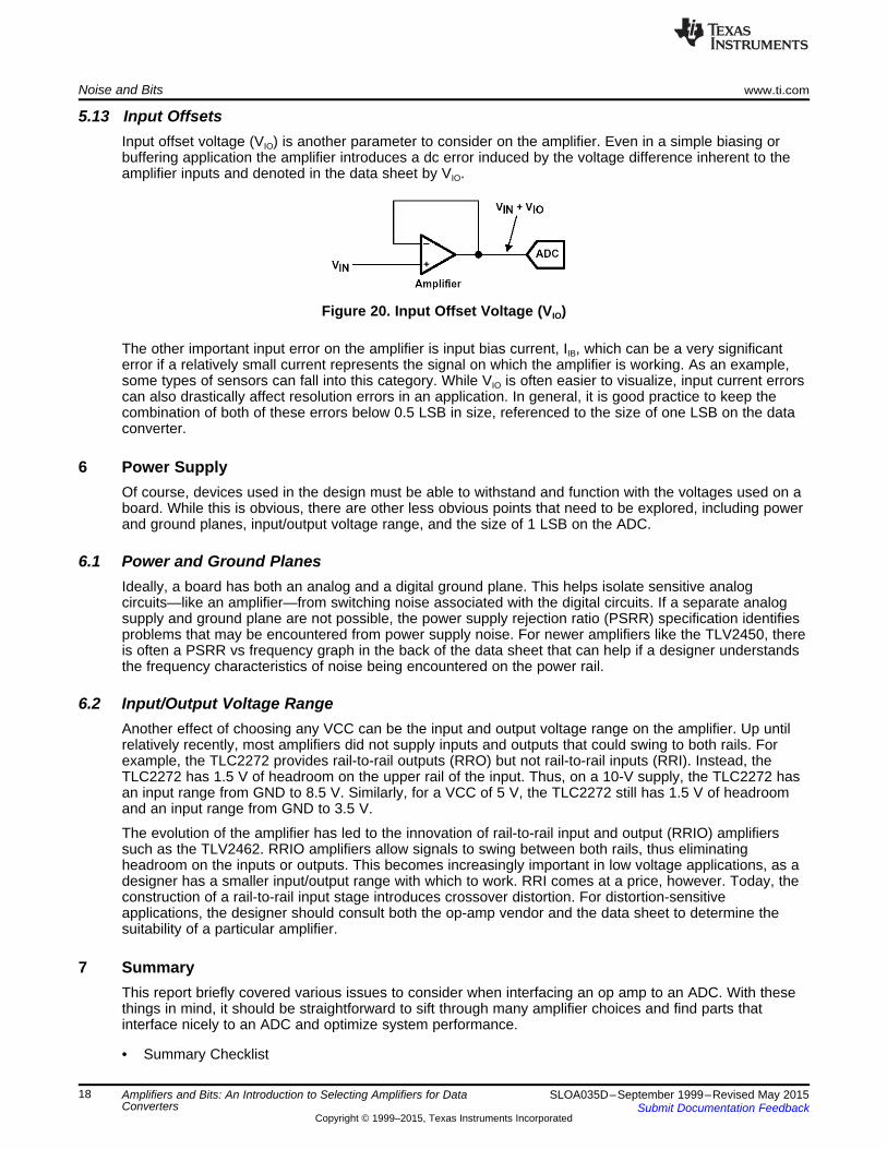
5.13 Input OffsetsInput offset voltage (VIO) is another parameter to consider on the amplifier. Even in a simple biasing orbuffering application the amplifier introduces a dc error induced by the voltage difference inherent to theamplifier inputs and denoted in the data sheet by VIO.
Figure 20. Input Offset Voltage (VIO)
The other important input error on the amplifier is input bias current, IIB, which can be a very significanterror if a relatively small current represents the signal on which the amplifier is working. As an example,some types of sensors can fall into this category. While VIO is often easier to visualize, input current errorscan also drastically affect resolution errors in an application. In general, it is good practice to keep thecombination of both of these errors below 0.5 LSB in size, referenced to the size of one LSB on the dataconverter.
6 Power SupplyOf course, devices used in the design must be able to withstand and function with the voltages used on aboard. While this is obvious, there are other less obvious points that need to be explored, including powerand ground planes, input/output voltage range, and the size of 1 LSB on the ADC.
6.1 Power and Ground PlanesIdeally, a board has both an analog and a digital ground plane. This helps isolate sensitive analogcircuits—like an amplifier—from switching noise associated with the digital circuits. If a separate analogsupply and ground plane are not possible, the power supply rejection ratio (PSRR) specification identifiesproblems that may be encountered from power supply noise. For newer amplifiers like the TLV2450, thereis often a PSRR vs frequency graph in the back of the data sheet that can help if a designer understandsthe frequency characteristics of noise being encountered on the power rail.
6.2 Input/Output Voltage RangeAnother effect of choosing any VCC can be the input and output voltage range on the amplifier. Up untilrelatively recently, most amplifiers did not supply inputs and outputs that could swing to both rails. Forexample, the TLC2272 provides rail-to-rail outputs (RRO) but not rail-to-rail inputs (RRI). Instead, theTLC2272 has 1.5 V of headroom on the upper rail of the input. Thus, on a 10-V supply, the TLC2272 hasan input range from GND to 8.5 V. Similarly, for a VCC of 5 V, the TLC2272 still has 1.5 V of headroomand an input range from GND to 3.5 V.
The evolution of the amplifier has led to the innovation of rail-to-rail input and output (RRIO) amplifierssuch as the TLV2462. RRIO amplifiers allow signals to swing between both rails, thus eliminatingheadroom on the inputs or outputs. This becomes increasingly important in low voltage applications, as adesigner has a smaller input/output range with which to work. RRI comes at a price, however. Today, theconstruction of a rail-to-rail input stage introduces crossover distortion. For distortion-sensitiveapplications, the designer should consult both the op-amp vendor and the data sheet to determine thesuitability of a particular amplifier.
7 SummaryThis report briefly covered various issues to consider when interfacing an op amp to an ADC. With thesethings in mind, it should be straightforward to sift through many amplifier choices and find parts thatinterface nicely to an ADC and optimize system performance.
• Summary Checklist
18 Amplifiers and Bits: An Introduction to Selecting Amplifiers for Data SLOA035D–September 1999–Revised May 2015Converters Submit Documentation Feedback
Copyright © 1999–2015, Texas Instruments Incorporated
www.ti.com References
– Bandwidth – amplifier GBP vs ADC speed– Resolution – amplifier SINAD vs ADC ENOB– Analog Input– –τ, drive current, and input signal vs ADC analog input range– Power – amplifier PSRR, amplifier I/O voltage range, and ADC LSB
8 References1. Electric Circuit Analysis Second Edition, by Johnson, Johnson, and Hilburn Copyright 1992, Prentice
Hall, Englewood Cliffs NJ2. DSP/Analog Technologies 1998 Seminar Series, by Texas Instruments Incorporated Copyright 19983. Op Amps for Everyone, Ron Mancini, Editor, Texas Instruments (SLOD006), Copyright 20004. Intuitive Operational Amplifier, Thomas M. Frederickson, Mc Graw Hill, Copyright 1988
19SLOA035D–September 1999–Revised May 2015 Amplifiers and Bits: An Introduction to Selecting Amplifiers for DataConvertersSubmit Documentation Feedback
Copyright © 1999–2015, Texas Instruments Incorporated
2s
qn
qP
12R=
Appendix A: Design Example – Cellular Telephone Base Station www.ti.com
9 Appendix A: Design Example – Cellular Telephone Base Station
9.1 ADC ConsiderationsAny discussion of the performance of a cellular base station design must center on the performance of thedata converter used to digitize the intermediate frequency (IF) bandwidth. The proper selection of dataconverter determines, to a large degree, the RF performance of the base station. Therefore, the choice ofdata converter is usually made long before the designer begins the design of an op amp interface. Thedesigner must make certain that the op amp interface does not act as a limiting function in overall systemperformance.
The dc nonlinearity performance is not nearly as important in a communications ADC as it is in aninstrumentation ADC because signals are band limited. The dynamic performance of the ADC is critical incommunications applications. The overall receiver system specifications depend heavily on ADC dynamicperformance. Characteristics of the data converter include:• Effective number of bits (ENOB) – is usually measured and specified at the system operating
frequency, so it is a real performance measurement.• Spurious Free dynamic range (SFDR) – determines the ADC’s ability to separate an incoming signal
from ADC noise spikes.• Total Harmonic Distortion (THD) – is a measure of the distortion that the ADC adds to the signal.• Signal-to-noise ratio (SNR) – includes ADC noise and noise from other sources.• Sampling Rate• Full scale range (FSR)
9.2 ADC Requirements for Processing GSM SignalThe data converter requirements for a cellular base station also depend on the communications protocolselected. The two most common are CDMA and GSM. This example focuses on GSM. It is beyond thescope of this document to examine the details of the GSM specification, but some of the high points are:• SNRTHERMAL = 9 dB for GSM-900• Process gain required = 24 dB (fS/BW)• Selected ADCSNR = 37 dB better than thermal• Baseband converter = 46 dB SNR• SNRADC = (46-24) = 22 dB• ENOB (effective number of bits) = (SNR-1.76) / 6.02 = 3.36 bits signal (4 bits required)• Interferer = 40 dB ≈ 6.3 bits
The mean squared quantization power is , where qs is the quantization step size and R is theADC input resistance, typically 600 Ω to 1000 Ω. Communication ADCs similar to the THS1052 andTHS1265 typically have a full-scale range (FSR) of 1 Vpp to 2 Vpp. Based on the assumption of a 50 Ωinput/output termination, the quantization noise power for a 12 bit, 65 MSPS ADC is –74 dBm. Thereceiver noise power in a noise-limited receiver can be computed as the thermal noise power in the givenreceiver BW plus the receiver noise figure.
For a 200 kHz BW GSM channel, TA = 25°C, and 4 to 6 dB NF, the receiver noise power is –115 dBm. Toboost the receiver noise to the quantization noise power level requires a gain of 42 dB. The smallest 1%bit error-rate (BER) for GSM-900 is –104 dBm, thus the SNR at baseband due to the thermal noisecomponent is given by SNRTHERMAL = Eb/No = –104 dBm +115 dBm = 9 dBm. For a raw BER to be 1% in aGSM system, testing and standard curves indicate that a baseband SNR of 9 dB is needed for thisperformance.
The process gain is Gp = fs / BW = 52 x 106 / 200 x 103 = 2.6 x 102 = 24 dB where the GSM channel BW is200 kHz and fs is 52 MHz (ADC sampling frequency). The converter noise at baseband should be muchbetter than the radio noise (thermal noise plus process gain), hence the converter noise at baseband =SNRADC + process gain (Gp).
20 Amplifiers and Bits: An Introduction to Selecting Amplifiers for Data SLOA035D–September 1999–Revised May 2015Converters Submit Documentation Feedback
Copyright © 1999–2015, Texas Instruments Incorporated
+
-
OPA685
C347 pF
C4
.1 μF
C5
4.7 pF
R5
49.9 Ω
R149.9 Ω
R2619 Ω
VOCM
VIN
R4
2 kΩ
R6
R3
619 Ω
C2100 nF
IN+
IN-
VOCM
ADS809
www.ti.com Appendix A: Design Example – Cellular Telephone Base Station
SNRADC is selected as 37 dB better than SNRTHERMAL; baseband converter noise is 9 dB + 37 dB = 45 dB.SNRADC required to meet the GSM-900 standard is (46-24) dB = 22 dB. The ENOB of the ADC must be =(SNR-1.76) / 6.02 at 4 bits. Assuming that the filter attenuates the interferer by 50 dB, the interferer dropsfrom 113 dBm to –53 dBm, or 40 dB above the GSM signal. The number of bits required to accommodatethe interferer is 40 dB / 6 dB / bit = 6.3 bits. Six bits are required to accommodate the interferer, 4 bits arerequired for the GSM signal, and 2 bits are required for headroom, so we need a 12-bit converter.
Table 3. Operational Amplifier Requirements
Parameter Value OPA685 UnitNoise voltage 2.7 to 8 2.7 nV/√HzNoise current 1 to 30 11.9 pA/√Hz
THD 70 to 95 82 dBcSlew Rate 260 to 3500 1700 V/µS
Small signal bandwidth 200 to 600 900 MHzLarge signal bandwidth ≥100 135 MHz
Common-mode input voltage 3 ±2.9 VSupply voltage ±5 ±5V V
Settling time 8 to 20 15 nSOutput current 40 to 100 80 mA
Output impedance ≤ 20 0.02 ΩPSRR -60 -64 dBCMRR -70 50 dB
Input offset voltage 10 ± 5 mV
The SFDR and IMD are the key ADC/DAC parameters that influence operational amplifier selection. Aminimum requirement is that the op amp’s SFDR or IMD, measured at the operating frequency, is 5 dB to10 dB better than the converter’s equivalent specifications. A perfect 12-bit ADC has a SFDR or IMD of 72dB, and the operational amplifier should have a SFDR or IMD of 77 dB to 82 dB. Fast settling time ismandatory because the ADC must settle within a fraction of an LSB in the ADC sampling time.
Low voltage systems are popular now, and the designer must be aware that ac specifications are onlyvalid at the test supply voltage. Operating the operational amplifier at different supply voltages changestheir ac specifications.
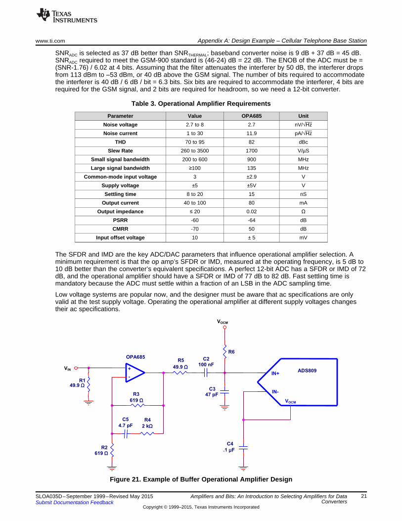
Figure 21. Example of Buffer Operational Amplifier Design
21SLOA035D–September 1999–Revised May 2015 Amplifiers and Bits: An Introduction to Selecting Amplifiers for DataConvertersSubmit Documentation Feedback
Copyright © 1999–2015, Texas Instruments Incorporated
Revision History www.ti.com
This is an example of an ADC buffer operational amplifier design. The input is terminated with R1, a49.9-Ω resistor. The OPA685 is a current feedback amplifier, operated at a noninverting gain of 2 (as setby R3 and R2). C5 and R4 are compensation components (never put a capacitor directly across thefeedback of a current feedback amplifier). The 49.9-Ω resistor in series with the amplifier output (R5), incombination with the 47 pF capacitor to ground (C3), are compensation for the input capacitance of theADC converter. R5 also isolates the output of the amplifier from a capacitive load. C2 ac-couples theamplifier output, and R6 to VOCM biases the input voltage up to the common mode range of the converter.Its value is not critical.
Revision History
Changes from C Revision (November 2010) to D Revision ........................................................................................... Page
• Changed format to current TI application report template. .......................................................................... 1
NOTE: Page numbers for previous revisions may differ from page numbers in the current version.
22 Revision History SLOA035D–September 1999–Revised May 2015Submit Documentation Feedback
Copyright © 1999–2015, Texas Instruments Incorporated
IMPORTANT NOTICE
Texas Instruments Incorporated and its subsidiaries (TI) reserve the right to make corrections, enhancements, improvements and otherchanges to its semiconductor products and services per JESD46, latest issue, and to discontinue any product or service per JESD48, latestissue. Buyers should obtain the latest relevant information before placing orders and should verify that such information is current andcomplete. All semiconductor products (also referred to herein as “components”) are sold subject to TI’s terms and conditions of salesupplied at the time of order acknowledgment.TI warrants performance of its components to the specifications applicable at the time of sale, in accordance with the warranty in TI’s termsand conditions of sale of semiconductor products. Testing and other quality control techniques are used to the extent TI deems necessaryto support this warranty. Except where mandated by applicable law, testing of all parameters of each component is not necessarilyperformed.TI assumes no liability for applications assistance or the design of Buyers’ products. Buyers are responsible for their products andapplications using TI components. To minimize the risks associated with Buyers’ products and applications, Buyers should provideadequate design and operating safeguards.TI does not warrant or represent that any license, either express or implied, is granted under any patent right, copyright, mask work right, orother intellectual property right relating to any combination, machine, or process in which TI components or services are used. Informationpublished by TI regarding third-party products or services does not constitute a license to use such products or services or a warranty orendorsement thereof. Use of such information may require a license from a third party under the patents or other intellectual property of thethird party, or a license from TI under the patents or other intellectual property of TI.Reproduction of significant portions of TI information in TI data books or data sheets is permissible only if reproduction is without alterationand is accompanied by all associated warranties, conditions, limitations, and notices. TI is not responsible or liable for such altereddocumentation. Information of third parties may be subject to additional restrictions.Resale of TI components or services with statements different from or beyond the parameters stated by TI for that component or servicevoids all express and any implied warranties for the associated TI component or service and is an unfair and deceptive business practice.TI is not responsible or liable for any such statements.Buyer acknowledges and agrees that it is solely responsible for compliance with all legal, regulatory and safety-related requirementsconcerning its products, and any use of TI components in its applications, notwithstanding any applications-related information or supportthat may be provided by TI. Buyer represents and agrees that it has all the necessary expertise to create and implement safeguards whichanticipate dangerous consequences of failures, monitor failures and their consequences, lessen the likelihood of failures that might causeharm and take appropriate remedial actions. Buyer will fully indemnify TI and its representatives against any damages arising out of the useof any TI components in safety-critical applications.In some cases, TI components may be promoted specifically to facilitate safety-related applications. With such components, TI’s goal is tohelp enable customers to design and create their own end-product solutions that meet applicable functional safety standards andrequirements. Nonetheless, such components are subject to these terms.No TI components are authorized for use in FDA Class III (or similar life-critical medical equipment) unless authorized officers of the partieshave executed a special agreement specifically governing such use.Only those TI components which TI has specifically designated as military grade or “enhanced plastic” are designed and intended for use inmilitary/aerospace applications or environments. Buyer acknowledges and agrees that any military or aerospace use of TI componentswhich have not been so designated is solely at the Buyer's risk, and that Buyer is solely responsible for compliance with all legal andregulatory requirements in connection with such use.TI has specifically designated certain components as meeting ISO/TS16949 requirements, mainly for automotive use. In any case of use ofnon-designated products, TI will not be responsible for any failure to meet ISO/TS16949.
Products ApplicationsAudio www.ti.com/audio Automotive and Transportation www.ti.com/automotiveAmplifiers amplifier.ti.com Communications and Telecom www.ti.com/communicationsData Converters dataconverter.ti.com Computers and Peripherals www.ti.com/computersDLP® Products www.dlp.com Consumer Electronics www.ti.com/consumer-appsDSP dsp.ti.com Energy and Lighting www.ti.com/energyClocks and Timers www.ti.com/clocks Industrial www.ti.com/industrialInterface interface.ti.com Medical www.ti.com/medicalLogic logic.ti.com Security www.ti.com/securityPower Mgmt power.ti.com Space, Avionics and Defense www.ti.com/space-avionics-defenseMicrocontrollers microcontroller.ti.com Video and Imaging www.ti.com/videoRFID www.ti-rfid.comOMAP Applications Processors www.ti.com/omap TI E2E Community e2e.ti.comWireless Connectivity www.ti.com/wirelessconnectivity
Mailing Address: Texas Instruments, Post Office Box 655303, Dallas, Texas 75265Copyright © 2015, Texas Instruments Incorporated