Embed Size (px)
Citation preview
Amorphous oxide alloys as interfacial layers withbroadly tunable electronic structures for organicphotovoltaic cellsNanjia Zhoua,b,1, Myung-Gil Kimc,1, Stephen Loserc, Jeremy Smithc, Hiroyuki Yoshidad, Xugang Guoa,b, Charles Songc,Hosub Jine, Zhihua Chenf, Seok Min Yoonc, Arthur J. Freemane, Robert P. H. Changa,b,2, Antonio Facchettic,f,2,and Tobin J. Marksa,b,c,2
aDepartment of Materials Science and Engineering, Northwestern University, Evanston, IL 60208; bArgonne Northwestern Solar Energy Research Center,Northwestern University, Evanston, IL 60208; cDepartment of Chemistry and the Materials Research Center, Northwestern University, Evanston, IL 60208;dGraduate School of Advanced Integration Science, Chiba University, Chiba, 263-8522, Japan; eDepartment of Physics, Northwestern University, Evanston,IL 60208; and fMaterials Department, Polyera Corporation, Skokie, IL 60077
Contributed by Tobin J. Marks, May 9, 2015 (sent for review March 5, 2015; reviewed by David Ginger and David S. Ginley)
In diverse classes of organic optoelectronic devices, controllingcharge injection, extraction, and blocking across organic semi-conductor–inorganic electrode interfaces is crucial for enhancingquantum efficiency and output voltage. To this end, the strategyof inserting engineered interfacial layers (IFLs) between electricalcontacts and organic semiconductors has significantly advancedorganic light-emitting diode and organic thin film transistor per-formance. For organic photovoltaic (OPV) devices, an electronicallyflexible IFL design strategy to incrementally tune energy levelmatching between the inorganic electrode system and the organicphotoactive components without varying the surface chemistrywould permit OPV cells to adapt to ever-changing generationsof photoactive materials. Here we report the implementation ofchemically/environmentally robust, low-temperature solution-pro-cessed amorphous transparent semiconducting oxide alloys, In-Ga-Oand Ga-Zn-Sn-O, as IFLs for inverted OPVs. Continuous variation ofthe IFL compositions tunes the conduction band minima over abroad range, affording optimized OPV power conversion efficien-cies for multiple classes of organic active layer materials and estab-lishing clear correlations between IFL/photoactive layer energeticsand device performance.
interface | amorphous oxide | photovoltaic | interfacial layers
Solar to electrical energy conversion technologies have re-ceived great attention as abundant and sustainable resources
(1–5). The diffuse nature of solar energy requires low-cost, large-area devices while maintaining high power conversion efficiency(PCE) (3). As a universal design strategy, many of the emergingthin film photovoltaic (PV) technologies such as bulk heterojunction(BHJ) organic, perovskite, quantum dot (QD), and CIGS (Cu-In-Ga-Se) solar cells are fabricated using a trilayer architecture, wherelight absorbers are sandwiched between two electrodes coated withvarious interfacial layers (IFLs) (6–9). Stringent requirements gov-ern ideal IFL materials design. Energetically, their respective bandpositions should match those of the photoinduced built-in potentialsto provide energetically continuous carrier transport pathways andto accommodate the maximum allowed output voltage. In re-cent reports, PV performance enhancement via IFL energetictuning has been demonstrated for very specific BHJ organic,QD, and perovskite cell compositions (6, 8, 10, 11). However,true IFL energetic tunability has not been achieved and offers achallenging opportunity to optimize device performance.Fabricable from energetically diverse organic active layers,
organic photovoltaics (OPVs) provide an excellent test bed fortuning IFL energetics and are the subject of this study. The basicBHJ OPV architecture contains a mesoscopically heterogeneousand isotropic, phase-separated donor–acceptor blend—a strategyto overcome the relatively short exciton diffusion lengths (∼10nm) (2, 12, 13), sandwiched between hole-transporting (HT) and
electron-transporting (ET) IFLs (2). These IFLs function to ac-commodate the cell built-in fields, to assist carrier extraction, andto suppress parasitic carrier recombination (2, 14–16). Indeed,studies on interfacial modification of HT electrodes verify thatchanging the band alignment profoundly affects OPV open circuitvoltage (Voc) and carrier lifetimes (17). Over the past decade,extensive efforts have focused on band gap engineering of OPVactive layer materials, mainly by tuning the donor material highestoccupied molecular orbital (HOMO) and lowest unoccupiedmolecular orbital (LUMO) energetics to enhance built-in poten-tials and maximize photon harvesting efficiency (18, 19). Conse-quently, compatible HT IFLs have been developed to tune theirvalence band minima (VBM) or HOMO energies to match that ofa specific organic donor. In contrast, because of historical limita-tions in acceptor diversity, far less effort has been devoted todeveloping ET IFLs—to date, a few ET IFLs have been used ininverted OPVs, primarily TiOx, ZnOx, several polymers, self-as-sembled monolayers, and cross-linked fullerenes (11, 14–16, 20–24). Nevertheless, most of these materials have fixed band edgepositions, significantly limiting their adaptability to emerging OPVmaterials systems with acceptors having different LUMO en-ergies. The recent emergence of promising nonfullerene OPV
Significance
The development of system-independent and non–material-spe-cific interfacial layers (IFLs) to facilitate efficient charge collectionis of crucial importance for organic photovoltaic (OPV) cell per-formance. Here we report a broadly applicable IFL design strat-egy using solution-processed amorphous oxide semiconductorswhere their energetics can be tuned by varying the elementalcomposition without varying the surface chemistry. Based on theenergetic requirements of specific organic active layers, theseoxides can be readily designed with dialed-in energy levels. UsingOPV solar cells as a test bed, we use a broad series of photoactivebulk heterojunction materials to demonstrate the effectivenessof these electronically tunable oxides for optimizing the perfor-mance of diverse OPV material sets.
Author contributions: N.Z., M.-G.K., R.P.H.C., A.F., and T.J.M. designed research; N.Z.,M.-G.K., S.L., J.S., H.Y., X.G., C.S., H.J., Z.C., S.M.Y., and A.J.F. performed research;N.Z., M.-G.K., S.L., J.S., H.Y., X.G., C.S., H.J., Z.C., S.M.Y., and A.J.F. analyzed data; andN.Z., M.-G.K., R.P.H.C., A.F., and T.J.M. wrote the paper.
Reviewers: D.G., University of Washington; and D.S.G., National Renewable EnergyLaboratory.
The authors declare no conflict of interest.1N.Z. and M.-G.K. contributed equally to this work.2To whom correspondence may be addressed. Email: [email protected], [email protected], or [email protected].
This article contains supporting information online at www.pnas.org/lookup/suppl/doi:10.1073/pnas.1508578112/-/DCSupplemental.
www.pnas.org/cgi/doi/10.1073/pnas.1508578112 PNAS | June 30, 2015 | vol. 112 | no. 26 | 7897–7902
CHEM
ISTR
Y
acceptors—n-type small molecules and polymers having diverseelectronic structures (1, 25–29)—illustrates the need for a de-sign strategy to create ET IFLs with broadly tunable energylevels. Furthermore, moving from oxides, to polymers, to self-assembled materials incurs large, unpredictable variations insurface chemistry, compounding the challenge in energy levelpositioning. Also, factors such as adsorbates, interfacial dipoles,molecular orientations, and interface states confound predictableIFL/organic semiconductor interfacial energy alignment (30)and challenge precise, continuous energy level tuning for tra-ditional organic semiconductor or vacuum deposited oxide IFLs.Thus, straightforwardly prepared ET IFL materials having broadlytunable conduction band minima (CBM) and work functions foradjusting band alignment would provide generalizable means tooptimize current generation OPV performance and accommodateemerging organic donor/acceptor pairs.We report here an ET IFL design strategy using solution-pro-
cessed amorphous metal oxide alloys. Continuous CBM tunabilityis achieved by alloying two or more electronically dissimilar ox-ides, realized by precursor compositional adjustment. We showthat band edge energies can be dialed-in for indium–gallium oxide(a-IGO) and gallium–zinc–tin oxide (a-GZTO) (Zn:Sn = 1:1) IFLs,providing CBM tunability over 3.5–4.6 eV. The resulting films haveexcellent chemical/environmental stability, conformal coating, andgood electron mobilities, ideal for solar cells as verified with severalOPV classes where the IFL CBMs are systematically tuned to op-timize performance. This includes acceptors with LUMO energiesfrom −4.1 eV to −3.5 eV. To our knowledge, these results are thefirst example of band structure tuning in solution-processed amor-phous oxide IFLs. Furthermore, the amorphous character enablesflexible OPV fabrication by coating amorphous oxide electrodes.Note that the oxide CBM energies and acceptor LUMO en-
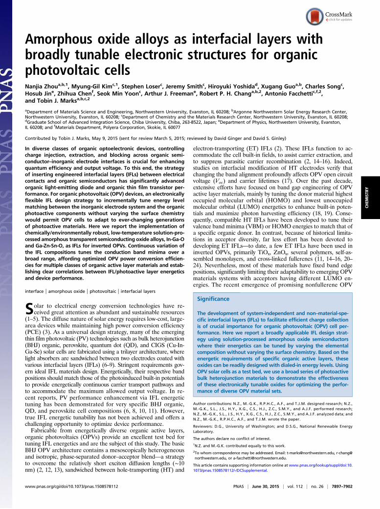
ergies are verified here by low-energy inverse photoemissionspectroscopy (LEIPS) which provides excellent energy resolutionand precision (∼0.1 eV) and negligible sample damage to or-ganics (31, 32) (see more in SI Appendix, Figs. S2 and S3). It willbe seen that OPV PV metrics closely track the IFL CBMs andcan be optimized for the five BHJ OPV material sets in Fig. 1B,PBDT-BTI:PDI-CN2; PTB7:PC71BM [poly[[4,8-bis[(2-ethylhexyl)oxy]-benzo[1,2-b:4,5-b’]dithiophene-2,6-diyl][3-fluoro-2-[(2-ethyl-hexyl)-carbonyl]-thieno[3,4-b]thiophenediyl]]:[6,6]-phenyl-C71-butyricacid methyl ester)] (33); PTB7:ICBA (PTB7: indene-C60 bisadduct)
(34); PTB7:P(NDI2OD-T2) [PTB7: poly[N,N’-bis(2-octyldodecyl)-naphthalene-1,4,5,8-bis(dicarboximide)-2,6-diyl]-alt-5,5′-(2,2’-bithiophene)] (35); and PDTG-TPD:PC71BM (poly-dithienogermole-thienopyrrolodione: PC71BM) (18).
Results and DiscussionIFL Design and Electronic Structure Characterization. Ideal OPVIFLs should achieve charge-selective transport with proper bandedge alignment and good optical transparency (14). For classicalpolycrystalline semiconductors such as GaAs-InAs, alloying chemi-cally similar constituents is known to achieve incremental band edgedisplacements (36–39). Olson et al. (39) achieved band alignment inpolycrystalline Zn1-xMgxO electrodes to reduce band offset in poly-mer-oxide solar cells and to maximize the Voc. Band gap manipu-lation is also possible in a-Si1-xGex:H materials (40). Amorphousoxide semiconductors generally have excellent optical transparency,smooth surfaces, mechanical flexibility, and highly dispersed ns-stateconduction bands with good electron mobility (41, 42). Furthermore,the excellent transport and optical properties of amorphous oxidesemiconductor-based transistors and transparent oxide conductorsargues that the low tail and midgap state densities should minimizeOPV recombination sites and yield electron-selective IFLs (41, 42).Additionally, the localized O 2p based valence bands, which aretypically deep and poorly dispersed, should block hole injection fromtypical organic donor HOMOs (43). Although compositional in-vestigations on amorphous oxides have been reported in Zn1-xBaxO,Zn1-xSrxO, and Ga1-xZnxO systems (44, 45), systematic band align-ment tuning via doping such oxides has not been demonstrated.In this study, In2O3, ZnO, and SnO2 are chosen as host matrices
because they have high electron mobilities and deep VBMs (46, 47)and, judging from ITO (Fig. 1B), should offer CBMs which spanthe LUMO energies of important classes of high-efficiency invertedOPV active layers. Ga2O3 is used as a dopant to shift the hostmatrix CBMs. It is known that bulk alloys of In2O3 + SnO2 withGa2O3 exhibit a broad range of amorphous phases, high opticaltransparency, and good electron mobilities (41, 46). Unlike capital-intensive physical vapor deposition techniques (pulsed laser de-position, sputtering, etc.), the fabrication of high-quality amorphousfilms is simple and achieved by mixing the metal precursor solutionsin the desired ratios, spin-coating in ambient, then annealing thefilms at moderate temperatures. This process is compatible withflexible plastic substrates. Fig. 1A shows a TEM cross-sectionalimage of a completed OPV with an a-IGO-50 (50% mol Ga) IFL.The nanobeam electron diffraction pattern reveals a halo, in-dicating amorphous character. Furthermore, mechanically flexibleOPVs can be fabricated using high-conductivity, amorphous zinc-indium-tin oxide (a-ZITO) electrodes on plastic substrates (48) (SIAppendix, Fig. S4). These double-layer amorphous electrodes arewell-matched in properties, yielding flexible devices with acceptableperformance versus their rigid counterparts. Also, using these IFLsin inverted OPVs enhances device ambient stability. Thus, PTB7:PC71BM inverted solar cells fabricated with a-IGO (60% Ga) ex-hibit excellent temporal stability (SI Appendix, Fig. S19), compa-rable to those reported using ZnO IFLs (20).To probe IFL film microstructure, composition, and surface
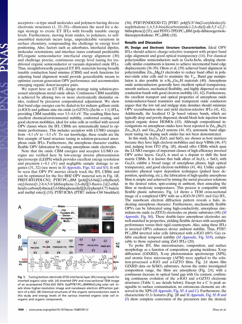
morphology as a function of composition, grazing incidence X-raydiffraction (GIXRD), X-ray photoemission spectroscopy (XPS),and atomic force microscopy (AFM) were applied to the solu-tion-processed a-IGO and a-GZTO films. Fig. 2A shows filmGIXRD data on Si/SiO2 substrates. Across the entire investigatedcomposition range, the films are amorphous (Fig. 2A), with acontinuous increase in optical band gap with Ga content, confirm-ing continuous evolution of the a-IGO and a-GZTO electronicstructures (Table 1; see details below). Except for a C 1s peak as-signable to surface contamination, no extraneous elements are ob-served in the XPS (SI Appendix, Fig. S5 A and C). Furthermore, thecharacteristic O 1s features (Fig. 2B and SI Appendix, Fig. S5 B andD) show complete conversion of the precursors into the desired,
Fig. 1. Tuning bottom electrode (ITO) interfacial layer (IFL) energy levels forinverted organic solar cells. (A) Inverted OPV and cross-sectional TEM imageof an as-prepared ITO/a-IGO (50% Ga)/PTB7:PC71BM/MoO3/Ag solar cell. In-sets show higher-resolution image and nanobeam electron diffraction pat-tern of a-IGO. (B) Chemical structures of the organic semiconductors used inthis study and energy levels of the various inverted organic solar cell in-organic and organic components.
7898 | www.pnas.org/cgi/doi/10.1073/pnas.1508578112 Zhou et al.
condensed oxide lattice. The lowest binding energy peak at ∼530–531 eV is assigned to the M-O-M lattice O, the peak at ∼531–532eV to M-OH or defect O, and the peak at ∼532–533 eV toadsorbed O species (46). Additionally, AFM data show that all ofthese films on glass/ITO substrates exhibit roughnesses <1.58 nm(Fig. 2C and SI Appendix, Fig. S6).Regarding IFL energy level tunability, if the CBMs are prin-
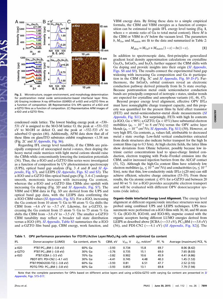
cipally composed of unoccupied metal s-states, then doping theheavy metal oxide matrices with light metal cations should raisethe CBMs while concomitantly lowering the ionization potentials(36). Thus, the a-IGO and a-GZTO film series were investigatedas a function of composition by UV photoemission spectroscopy(UPS), optical band gap analysis (Fig. 3 A and B and SI Ap-pendix, Fig. S7), and LEIPS (SI Appendix, Figs. S2 and S3). Thea-IGO and a-GZTO film optical band gaps (Fig. 3 A–C) undergosmooth, monotonic increases with increasing Ga content,whereas the a-IGO and a-GZTO film CBMs also upshift withincreasing Ga doping (Fig. 3D and SI Appendix, Fig. S7). TheVBM and CBM data in Fig. 3D are derived from the UPS andoptical band gap data, with the LEIPS data confirming thea-IGO CBM values (SI Appendix, Fig. S3). For a-IGO, increasingthe Ga content from 10 atom % Ga to 90 atom % Ga shifts theCBM from −4.6 eV to −3.7 eV. Likewise, for a-GZTO, in-creasing the Ga content from 15 atom % Ga to 75 atom % Gashifts the CBM from −3.8 eV to −3.5 eV. The smaller a-GZTOCBM tunability may reflect a broader tail state distributionversus a-IGO (49). SI Appendix, Table S3 summarizes the a-IGOand a-GZTO film band gap, CBM energy, work function, and
VBM energy data. By fitting these data to a simple empiricalformula, the CBM and VBM energies as a function of compo-sition can be estimated to guide IFL energy level tuning (Eq. 1,where x = atomic ratio of Ga to total metal content). Here M isthe CBM or VBM in eV below the vacuum level. The parametersb, MGa, and Mmatrix are fit to the data and summarized in Table 2:
Malloy =MGax+Mmatrixð1− xÞ− bxð1− xÞ. [1]
In addition to spectroscopic data, first-principles generalizedgradient local density approximation calculations on crystallineGa2O3, InGaO3, and In2O3 further support the CBM shifts withGa doping and provide insights into their origin (SI Appendix,Figs. S8 and S9). The results connect the experimental band gapwidening with increasing Ga composition and Ga 4s participa-tion in the CBM (Fig. 3C and SI Appendix, Fig. S9 D–F). Fur-thermore, the InGaO3 orbital contours reveal an electronicconduction pathway derived primarily from In 5s state overlap.Because posttransition metal oxide semiconductor conductionbands are principally composed of isotropic s states, similar trendsare expected for crystalline and amorphous variants (41, 46, 47).Beyond proper energy level alignment, effective OPV IFLs
must have nonnegligible charge transport capacity, and this prop-erty was quantified for the present films by field effect transistor(FET) and metal–semiconductor–metal diode measurements (SIAppendix, Fig. S11). Not surprisingly, FETs with high In contents(a-IGO, Ga < 90%; a-GZTO, Ga < 45%) have substantial electronmobilities (μe ∼ 10−3 to 8 cm2/Vs) versus the OPV active layerblends (μe ∼ 10−4 cm2/Vs; SI Appendix, Fig. S11) (50). However, atvery high IFL Ga contents, μe values fall, attributable to decreasedmetal s state overlap. Low-field vertical conductivities extractedfrom diode structures also indicate better transport for the high Incontent films (up to 0.3 S/m). At high electric fields, the latter filmsshow deviations from Ohmic behavior, possibly because low in-trinsic carrier concentrations lead to space-charge limited con-duction, electron trapping with Poole–Frenkel emission into theCBM, and/or increased injection barriers from the Al/CsF contact(51, 52). Although the high-Ga content films have relatively lowelectron mobilities (μe ≤ 10−4 cm2/Vs) and conductivities (σ0 ≤ 10−5
S/m), note that thin, low-conductivity oxide IFLs (≤20 nm) can stillachieve efficient, selective charge extraction (53–55). From theseresults, the Ga atomic content ≤ 45% for a-GZTO and between 20and 80 wt % for a-IGO provides acceptable electron transportand will be evaluated with different OPV donor/acceptor sys-tems (vide infra).
Organic–Oxide Interfacial Energy Level Alignment. The energy levelalignment at different organic/oxide interface structures was nextprobed using combined UPS and LEIPS techniques. UPS mea-surements were performed on a-IGO films with 30, 60, and 80 atom% Ga (IGO-30, IGO-60, and IGO-80), stepwise coated with theorganic acceptors having different LUMO energies derived fromLEIPS as described above [ICBA (∼−3.5 eV), PC71BM (∼−3.8 eV)(56), and PDI-CN2 (∼−4.1 eV) (SI Appendix, Fig. S2)]. The
Fig. 2. Microstructure, oxygen environment, and morphology determinationfor posttransition metal oxide semiconductor-based interfacial layer films.(A) Grazing incidence X-ray diffraction (GIXRD) of a-IGO and a-GZTO films asa function of composition. (B) Representative O1s XPS spectra of a-IGO anda-GZTO films as a function of composition. (C) Representative AFM images ofa-IGO and a-GZTO films.
Table 1. OPV performance parameters for ITO/IFL/Active Layer/MoO3/Ag cells with optimized Ga content
IFL Donor:acceptor (LUMO) Ga content, atom % CBM, eV VOC, V JSC, mA/cm2 FF, % Average (maximum) PCE, %
a-IGO PTB7:PC71BM (−3.8 eV) 60% Ga −3.93 0.734 15.8 69.7 8.06 (8.42)a-GZTO PTB7:PC71BM (−3.8 eV) 30% Ga −3.76 0.735 15.1 69.0 7.65 (8.03)a-IGO PTB7:ICBA (−3.5 eV) 70% Ga −3.82 0.902 10.6 45.9 4.41 (4.86)
PBDT-BTI: PDI-CN2 (−4.1 eV) 30% Ga −4.41 0.745 4.48 40.3 1.45 (1.53)PTB7:P(NDI2OD-T2) (−3.8 eV) 60% Ga −3.93 0.81 6.51 47.7 2.52 (2.55)PDTG-TPD: PC71BM (−3.8 eV) 60% Ga −3.93 0.853 13.1 69.8 7.79 (7.94)
Note that the complete parameters for OPVs based on different active layers and using a-IGO/a-GZTO with varying Ga content are presented in SIAppendix, Figs. S15–S17.
Zhou et al. PNAS | June 30, 2015 | vol. 112 | no. 26 | 7899
CHEM
ISTR
Y
complete energy level diagrams of the organic-coated oxides areshown in SI Appendix, Figs. S12–S14. Note that the vacuum levelshifts are determined from the UPS cutoff energies of the secondaryelectrons. The LUMO energies are determined by LEIPS for theorganic acceptors, whereas the oxide CBMs are from the VBM +optical bandgaps (Fig. 2A and SI Appendix, Fig. S7) because theoxide exciton binding energies are expected to be negligible.Comparing different a-IGO/organic junctions in SI Appendix, Figs.S12–S14, important differences are found in the energy offsets,ΔELUMO-acceptor – ECBM-oxide, for the different a-IGO/organic junc-tions. For ICBA, this offset decreases going from IGO-30 (∼0.7 eV)and IGO-60 (∼0.7 eV) to IGO-80 (∼0.2 eV) (SI Appendix, Figs. S12–S14). It is therefore expected that IGO-80 offers preferential energyalignment for ICBA-based OPVs. The large energy offsets betweenthis acceptor and a-IGOswithGa content<80 atom%will likely leadto thermionic losses for electron collection (39, 57). For PC71BM, theLUMO energy matches with the IGO-60 and IGO-80 CBMs rela-tively well. Last, for PDI-CN2, the energy offset is minimized forIGO-30 and IGO-60, whereas its LUMOenergy is located well belowthe CBM of IGO-80, likely creating a charge injection barrier whichimpedes transport through these junctions and promotes surfacerecombination (39, 58, 59) (SI Appendix, Figs. S12–S14).
Inverted OPV Performance. To investigate oxide IFL effects onOPV performance, device response was evaluated as a functionof (i) a-IGO vs. a-GZTO IFL compositions with the same BHJactive layer donor–acceptor blend, (ii) IFL effects with BHJacceptors having different LUMO energies, and (iii) the sameBHJ donor with acceptors possessing the similar LUMO ener-gies. In the first study, PTB7:PC71BM cells were fabricated usingboth a-IGO and a-GZTO IFLs to define the composition effects.From the results in SI Appendix, Fig. S12, the energy offset be-tween ICBA and IGO-80 is minimized, whereas lower atom %Ga causes unfavorable energy alignment with ICBA. SI Appen-dix, Fig. S18, shows the trend of Voc, short circuit currents (Jscs),fill factors (FFs), and PCEs for PTB7:PCBM cells fabricatedon a-IGO and a-GZTO with varying Ga contents. As shown in
SI Appendix, Fig. S18 B–D, the Jscs, FFs, and PCEs of deviceswith both a-IGO and a-GZTO initially rise with increasing Gacontent (although the conductivities of both IFLs are similar),then fall for higher Ga contents in both oxide families. Themaximum performance occurs at 60–70 atom % Ga (CBM =∼−3.93 to −3.82) and 30 atom % Ga (CBM = −3.76) for a-IGOand a-GZTO, respectively, which indicates that the CBM levelsare optimally positioned relative to the PC71BM LUMO, asshown in Table 1 and SI Appendix, Fig. S18 and Table S6. Theincreased Jsc, FF, and PCE parameters can be attributed to thefavorable alignment noted above between the ICBA LUMO andthe IFL CBMs. The fact that both oxides function optimally whenCBM energies match the LUMO energies of PC71BM provides aninternal consistency check and strongly confirms the generality ofthe present IFL energetic tuning strategy for different oxides.In the second set of experiments, a-IGO composition effects
were investigated for BHJ OPVs with acceptors having differentLUMO energies. Regarding donors, PTB7 was used with ICBA(and PC71BM), whereas the low-lying HOMO polymer PBDT-BTI was used in combination with PDI-CN2 because it affordsa large Voc. As noted above, broad IFL CBM tunability to ac-commodate current and emerging BHJ acceptors is a critical taskfor next-generation OPVs. As shown in SI Appendix, Figs. S12–S14, the combination of IGO-80/ICBA, IGO-60 or IGO-80/PC71BM, and IGO-30 or IGO-60/PDI-CN2 achieves optimalenergy level alignment and minimum energy offsets (<0.2 eV) inthe corresponding heterojunctions. From the data in Fig. 4 E–Hand SI Appendix, Fig. S16, the resulting OPVs using these threeacceptors indeed exhibit maximum performance for the optimalIFL–acceptor pairing. For all three active layer/oxide combina-tions, PTB7:ICBA, PTB7:PC71BM, and PBDT-BTI:PDI-CN2, thedevice characteristics agree well with the UPS/LEIPS-derived energyalignment results, showing optimal device metrics at 70–80, 60–70,and 30–60 atom % Ga, respectively. Besides the trend in PCE, thevariations in FF also closely track the ΔELUMO-acceptor – ECBM-oxideenergy offsets described above. This finding confirms that interfacialenergy alignment has a direct consequence for device FF attributedto variation of interfacial charge transport properties which ulti-mately affect the OPV series and shunt resistance (10, 17, 60,61). From these results, the significance of IFL CBM tuning foremerging OPV systems is clearly evident.Finally, to probe the generality with other donor–acceptor pairs,
IFL effects were investigated for OPVs based on three well-studiedhigh-performance OPV systems with PC71BM and P(NDI2OD-T2) as the acceptors. The results for PTB7:PC71BM (describedabove), dithienogermole-thienopyrrolodione (PDTG-TPD):PC71BM,and PTB7:P(NDI2OD-T2) all-polymer solar cells (11, 18, 27) arecompared in SI Appendix, Fig. S17 and Tables S8 and S9. Despitelarge differences in chemical and structural properties, bothPC71BM and P(NDI2OD-T2) have similar ELUMO = ∼−3.8 eV(SI Appendix, Fig. S2) (56), and although absolute performancemetrics differ, note that the metrics of all three OPV typesconsistently track each other, reaching performance maxima at60 atom % Ga (CBM = −3.93 eV).
Fig. 3. Tuning the band edges of amorphous oxide semiconductors viacomposition. (A) Plots showing band gap derivation from optical trans-mission spectra for a-IGO films as a function of Ga content. (B) Represen-tative UPS spectra of a-IGO films as a function of atom % Ga content.(C) Optical band gap dependence on Ga content in a-IGO and a-GZTO films.(D) CBM and VBM energy dependences on atom % Ga content in a-IGO anda-GZTO films determined by UPS and the measured optical band gap.
Table 2. Fitting parameters for the empirical Eq. 1 describingthe variation of CBM and VBM with Ga content in a-IGO anda-GZTO films
Material MGa, eV Mmatrix, eV b, eV
a-IGOVBM 7.88 7.00 0.70CBM 3.50 4.73 0.60
a-GZTOVBM 7.70 7.37 0.08CBM 3.20 3.87 −0.47
7900 | www.pnas.org/cgi/doi/10.1073/pnas.1508578112 Zhou et al.
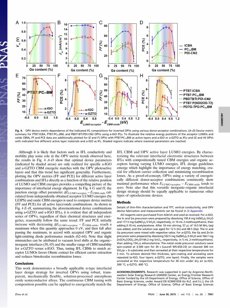
Although it is likely that factors such as IFL conductivity andmobility play some role in the OPV metric trends observed here,the results in Fig. 4 A–D show that optimal device parameters(indicated by shaded areas) are only realized for specific a-IGOand a-GZTO CBM energetic matches with the OPV photoactivelayers and that this trend has significant generality. Furthermore,plotting the OPV metrics (FF and PCE) for different active layercombinations and IFLs directly as a function of the relative positionof LUMO and CBM energies provides a compelling picture of theimportance of interfacial energy alignment. In Fig. 4 G and H, thejunction energy offset parameter ΔELUMO-acceptor – ECBM-oxide cal-culated from independently obtained acceptor LUMO energies (byLEIPS) and oxide CBM energies is used to compare device metrics(FF and PCE) for all active layer/oxide combinations. As shown inFig. 4 E–H, summarizing the aforementioned device combinationsusing a-GZTO and a-IGO IFLs, it is evident that all independentseries of OPVs, regardless of their chemical structures and ener-getics, reasonably follow the same trend: FF and PCE initiallyincrease with decreasing ΔELUMO-acceptor – ECBM-oxide, reach amaximum when this quantity approaches 0 eV, and then fall afterpassing the maximum, in accord with accepted OPV and organiclight-emitting diode performance models (62–64). Note that slightmismatches can be attributed to vacuum level shifts at the organic–inorganic interfaces (30, 65) and the smaller range of CBM tunabilityfor a-GZTO versus a-IGO. Thus, tuning IFL CBMs to match ac-ceptor LUMOs favors Ohmic contact for efficient carrier extractionand reduces bimolecular recombination losses.
ConclusionsThis work demonstrates a broadly applicable n-type interfaciallayer design strategy for inverted OPVs using robust, trans-parent, mechanically flexible, solution-processed amorphousoxide semiconductor alloys. The continuous CBM tuning withcomposition possible can be applied to energetically match the
IFL CBM and OPV active layer LUMO energies. By charac-terizing the relevant interfacial electronic structures betweenIFLs with compositionally tuned CBM energies and organic ac-ceptors having varying LUMO energies, IFL design guidelinesemerge which highlight the importance of energy matching, cru-cial for efficient carrier collection and minimizing recombinationlosses. As a proof-of-concept, OPVs using a variety of energeti-cally different donor:acceptor combinations consistently showmaximal performance when ELUMO-acceptor – ECBM-oxide tends tozero. Note also that this versatile inorganic–organic interfacialdesign strategy should be equally applicable to numerous othertypes of optoelectronic devices.
MethodsDetails of thin-film characterization and TFT, vertical conductivity, and OPVdevice fabrication and measurements can be found in SI Appendix.
All reagents were purchased from Aldrich and used as received. For a-IGO,the In and Ga precursors were prepared by dissolving 195.4 mg In(NO3)3·5H2Oand 177.5 mg Ga(NO3)3·5·5H2O, respectively, in 10 mL 2-methoxyethanol, thenadding 0.10 mL acetylacetone. After 10 min stirring, 57 μL of 14.5 M NH3 (aq)was added, and the solution was aged for 12 h (In) and 48 h (Ga). The In andGa precursors were mixed with respective ratios. For a-GZTO, the Ga and Zn-Snprecursors were prepared by dissolving 532.5 mg Ga(NO3)3·5.5H2O and 164.7 mgZn(CH3COO)2·2H2O/144.2 mg SnCl2, respectively, in 5 mL 2-methoxyethanol,then adding 154 μL ethanolamine. The metal oxide precursor solutions werespin-coated at 3,500 rpm for 30 s (Laurell WS-650-23) on cleaned 300 nmSiO2/p + Si substrates and then annealed at their respective temperatures for5 min. To achieve desired film thickness, spin-coating and annealing wererepeated (a-IGO, four layers; a-GZTO, one layer). Finally, the samples wereannealed at the respective temperature for 30 min under dry air (a-IGO,300 °C; a-GZTO, 400 °C).
ACKNOWLEDGMENTS. Research was supported in part by Argonne–North-western Solar Energy Research (ANSER) Center, an Energy Frontier ResearchCenter funded by the US Department of Energy, Office of Science, Office ofBasic Energy Sciences, under Award DE-SC0001059 (to N.Z. and S.L.); the USDepartment of Energy, Office of Science, Office of Basic Energy Sciences
Fig. 4. OPV device metric dependence of the indicated IFL compositions for inverted OPVs using various donor:acceptor combinations. (A–D) Device metricsummary for PTB7:ICBA, PTB7:PC71BM, and PBDT-BTI:PDI-CN2 OPVs using a-IGO IFLs. To illustrate the relative energy positions of the acceptor LUMOs andoxide CBMs, FF and PCE data are additionally plotted for (E and F) OPVs with PTB7:PC71BM as active layers and a-IGO or a-GZTO as IFLs and (G and H) OPVswith indicated five different active layer materials and a-IGO as IFL. Shaded regions indicate where maximal parameters are reached.
Zhou et al. PNAS | June 30, 2015 | vol. 112 | no. 26 | 7901
CHEM
ISTR
Y
under Award DE-FG02-08ER46536 (to C.S., S.M.Y., A.J.F., and H.J.); Office ofNaval Research Multi-University Research Initiative (ONR MURI) N00014-11-1-0690 (to J.S.); Japan Science and Technology Office Presto and Japan So-ciety for the Promotion of Science KAKENHI Grant 26288007 (to H.Y.); andthe Northwestern University Materials Research Science and Engineering
Center under National Science Foundation (NSF) Grant DMR-1121262 (toM.-G.K.). We thank the Integrated Molecular Structure Education andResearch Center (IMSERC) for characterization facilities supported by North-western University, NSF under NSF CHE-0923236 and CHE-9871268 (1998),Pfizer, and the State of Illinois.
1. Anthony JE (2010) Small-molecule, nonfullerene acceptors for polymer bulk hetero-junction organic photovoltaics. Chem Mater 23(3):583–590.
2. Li G, Zhu R, Yang Y (2012) Polymer solar cells. Nat Photonics 6(3):153–161.3. Lewis NS, Nocera DG (2006) Powering the planet: Chemical challenges in solar energy
utilization. Proc Natl Acad Sci USA 103(43):15729–15735.4. Lipomi DJ, Bao Z (2011) Stretchable, elastic materials and devices for solar energy
conversion. Energy Environ Sci 4(9):3314–3328.5. Jeong S, et al. (2012) Hybrid silicon nanocone-polymer solar cells. Nano Lett 12(6):
2971–2976.6. Zhou H, et al. (2014) Photovoltaics. Interface engineering of highly efficient perov-
skite solar cells. Science 345(6196):542–546.7. Snaith HJ (2013) Perovskites: The emergence of a new era for low-cost, high-efficiency
solar cells. J Phys Chem Lett 4(21):3623–3630.8. Chuang C-HM, Brown PR, Bulovi�c V, BawendiMG (2014) Improved performance and stability
in quantum dot solar cells through band alignment engineering. Nat Mater 13(8):796–801.9. Repins I, et al. (2008) 19·9%-efficient ZnO/CdS/CuInGaSe2 solar cell with 81·2% fill
factor. Prog Photovolt Res Appl 16(3):235–239.10. Chen L-M, Xu Z, Hong Z, Yang Y (2010) Interface investigation and engineering—Achieving
high performance polymer photovoltaic devices. J Mater Chem 20(13):2575–2598.11. He Z, et al. (2012) Enhanced power-conversion efficiency in polymer solar cells using
an inverted device structure. Nat Photonics 6(9):591–595.12. Bartelt JA, et al. (2013) The importance of fullerene percolation in the mixed regions
of polymer–fullerene bulk heterojunction solar cells. Adv Energy Mater 3(3):364–374.13. Yu G, Gao J, Hummelen JC, Wudl F, Heeger AJ (1995) Polymer photovoltaic cells:
Enhanced efficiencies via a network of internal donor-acceptor heterojunctions. Sci-ence 270(5243):1789–1791.
14. Steim R, Kogler FR, Brabec CJ (2010) Interface materials for organic solar cells. J MaterChem 20(13):2499–2512.
15. Zhou Y, et al. (2012) A universal method to produce low-work function electrodes fororganic electronics. Science 336(6079):327–332.
16. Ma H, Yip H-L, Huang F, Jen AKY (2010) Interface engineering for organic electronics.Adv Funct Mater 20(9):1371–1388.
17. Knesting KM, et al. (2013) ITO interface modifiers can improve VOC in polymer solarcells and suppress surface recombination. J Phys Chem Lett 4(23):4038–4044.
18. Small CE, et al. (2012) High-efficiency inverted dithienogermole-thienopyrrolodione-based polymer solar cells. Nat Photonics 6(2):115–120.
19. You J, et al. (2013) A polymer tandem solar cell with 10.6% power conversion effi-ciency. Nat Commun 4:1446.
20. Sun Y, Seo JH, Takacs CJ, Seifter J, Heeger AJ (2011) Inverted polymer solar cells in-tegrated with a low-temperature-annealed sol-gel-derived ZnO Film as an electrontransport layer. Adv Mater 23(14):1679–1683.
21. Ahlswede E, Hanisch J, Powalla M (2007) Comparative study of the influence of LiF,NaF, and KF on the performance of polymer bulk heterojunction solar cells. Appl PhysLett 90(16):163504.
22. Kim JY, et al. (2007) Efficient tandem polymer solar cells fabricated by all-solutionprocessing. Science 317(5835):222–225.
23. Hsieh C-H, et al. (2010) Highly efficient and stable inverted polymer solar cells in-tegrated with a cross-linked fullerene material as an interlayer. J Am Chem Soc132(13):4887–4893.
24. Litzov I, Brabec C (2013) Development of efficient and stable inverted bulk hetero-junction (BHJ) solar cells using different metal oxide interfaces. Materials 6(12):5796–5820.
25. Holcombe TW, et al. (2011) Steric control of the donor/acceptor interface: Implications inorganic photovoltaic charge generation. J Am Chem Soc 133(31):12106–12114.
26. Moore JR, et al. (2011) Polymer blend solar cells based on a high-mobility naph-thalenediimide-based polymer acceptor: Device physics, photophysics and morphol-ogy. Adv Energy Mater 1(2):230–240.
27. Zhou N, et al. (2014) Morphology-performance relationships in high-efficiency all-polymer solar cells. Adv Energy Mater 4(3):1300785.
28. Zang Y, et al. (2014) Integrated molecular, interfacial, and device engineering towardshigh-performance non-fullerene based organic solar cells. Adv Mater 26(32):5708–5714.
29. Mori D, Benten H, Okada I, Ohkita H, Ito S (2014) Highly efficient charge-carriergeneration and collection in polymer/polymer blend solar cells with a power con-version efficiency of 5.7%. Energy Environ Sci 7(9):2939–2943.
30. Ishii H, Sugiyama K, Ito E, Seki K (1999) Energy level alignment and interfacial electronicstructures at organic/metal and organic/organic interfaces. Adv Mater 11(8):605–625.
31. Yoshida H (2012) Near-ultraviolet inverse photoemission spectroscopy using ultra-lowenergy electrons. Chem Phys Lett 539-540(29):180–185.
32. Yoshida H (2014) Measuring the electron affinity of organic solids: An indispensablenew tool for organic electronics. Anal Bioanal Chem 406(9-10):2231–2237.
33. Liang Y, et al. (2010) For the bright future-bulk heterojunction polymer solar cellswith power conversion efficiency of 7.4%. Adv Mater 22(20):E135–E138.
34. He Y, Chen H-Y, Hou J, Li Y (2010) Indene-C(60) bisadduct: A new acceptor for high-performance polymer solar cells. J Am Chem Soc 132(4):1377–1382.
35. Yan H, et al. (2009) A high-mobility electron-transporting polymer for printed tran-sistors. Nature 457(7230):679–686.
36. Wang ZJ, Tanaka I (2009) Conduction-band structures of wurtzite ZnO solid solutionsby first principles calculations. Mater Trans 50(5):1067–1070.
37. Wei S-H, Zhang SB, Zunger A (2000) First-principles calculation of band offsets, opticalbowings, and defects in CdS, CdSe, CdTe, and their alloys. J Appl Phys 87(3):1304–1311.
38. Dolginov LM, Eliseev PG, Mil’vidskiı̆ MG (1976) Multicomponent semiconductor solidsolutions and their laser applications. Sov J Quantum Electron 6(7):1381–1393.
39. Olson DC, et al. (2007) Band-offset engineering for enhanced open-circuit voltage inpolymer–oxide hybrid solar cells. Adv Funct Mater 17(2):264–269.
40. Stutzmann M, Street RA, Tsai CC, Boyce JB, Ready SE (1989) Structural, optical, and spinproperties of hydrogenated amorphous silicon-germanium alloys. J Appl Phys 66(2):569–592.
41. Kamiya T, Hosono H (2010) Material characteristics and applications of transparentamorphous oxide semiconductors. NPG Asia Mater 2(1):15–22.
42. Perkins JD, et al. (2010) Amorphous transparent conductors for PV applications. 201035th IEEE Photovoltaic Specialists Conference (PVSC) (Inst Electr Electron Eng, NewYork), pp 000989–000991.
43. Walsh A, Da Silva JLF, Yan Y, Al-Jassim MM, Wei S-H (2009) Origin of electronic andoptical trends in ternary In2O3(ZnO)n transparent conducting oxides (n=1,3,5): Hy-brid density functional theory calculations. Phys Rev B 79(7):073105.
44. Pachoumi O, Li C, Vaynzof Y, Banger KK, Sirringhaus H (2013) Improved performanceand stability of inverted organic solar cells with sol–gel processed, amorphous mixedmetal oxide electron extraction layers comprising alkaline earth metals. Adv EnergyMater 3(11):1428–1436.
45. Ratcliff EL, et al. (2012) Surface composition, work function, and electrochemicalcharacteristics of gallium-doped zinc oxide. Thin Solid Films 520(17):5652–5663.
46. KimM-G, Kanatzidis MG, Facchetti A, Marks TJ (2011) Low-temperature fabrication ofhigh-performance metal oxide thin-film electronics via combustion processing. NatMater 10(5):382–388.
47. Charlene C, Kai-Chen C, Evgeniy C, Jerzy K (2011) Crystalline In–Ga–Zn–O density ofstates and energy band structure calculation using density function theory. Jpn J ApplPhys 50(9R):091102.
48. Zhou N, et al. (2014) Ultraflexible polymer solar cells using amorphous zinc-indium-tinoxide transparent electrodes. Adv Mater 26(7):1098–1104.
49. Hosono H, Nomura K, Ogo Y, Uruga T, Kamiya T (2008) Factors controlling electrontransport properties in transparent amorphous oxide semiconductors. J Non-CrystSolids 354(19-25):2796–2800.
50. Nakamura J-i, Murata K, Takahashi K (2005) Relation between carrier mobility andcell performance in bulk heterojunction solar cells consisting of soluble poly-thiophene and fullerene derivatives. Appl Phys Lett 87(13):132105.
51. O’Dwyer JJ (1973) The Theory of Electrical Conduction and Breakdown in Solid Di-electrics (Clarendon Press, Oxford).
52. Lovejoy TC, et al. (2012) Band bending and surface defects in β-Ga2O3. Appl Phys Lett100(18):181602.
53. Irwin MD, et al. (2011) Structural and electrical functionality of NiO interfacial films inbulk heterojunction organic solar cells. Chem Mater 23(8):2218–2226.
54. Stubhan T, et al. (2013) Overcoming interface losses in organic solar cells by applyinglow temperature, solution processed aluminum-doped zinc oxide electron extractionlayers. J Mater Chem A 1(19):6004–6009.
55. Ratcliff EL, et al. (2013) Investigating the influence of interfacial contact properties onopen circuit voltages in organic photovoltaic performance: Work function versusselectivity. Adv Energy Mater 3(5):647–656.
56. Yoshida H (2014) Low-energy inverse photoemission study on the electron affinities offullerene derivatives for organic photovoltaic cells. J Phys Chem C 118(42):24377–24382.
57. Schulz P, et al. (2014) Interface energetics in organo-metal halide perovskite-basedphotovoltaic cells. Energy Environ Sci 7(4):1377–1381.
58. Blumstengel S, et al. (2010) Band-offset engineering in organic/inorganic semi-conductor hybrid structures. Phys Chem Chem Phys 12(37):11642–11646.
59. Braun S, SalaneckWR, FahlmanM (2009) Energy-level alignment at organic/metal andorganic/organic interfaces. Adv Mater 21(14-15):1450–1472.
60. Guerrero A, Ripolles-Sanchis T, Boix PP, Garcia-Belmonte G (2012) Series resistance inorganic bulk-heterojunction solar devices: Modulating carrier transport with fuller-ene electron traps. Org Electron 13(11):2326–2332.
61. Cowan SR, et al. (2014) Chemically controlled reversible and irreversible extractionbarriers via stable interface modification of zinc oxide electron collection layer inpolycarbazole-based organic solar cells. Adv Funct Mater 24(29):4671–4680.
62. Veinot JGC, Marks TJ (2005) Toward the ideal organic light-emitting diode. Theversatility and utility of interfacial tailoring by cross-linked siloxane interlayers. AccChem Res 38(8):632–643.
63. Scharber MC, et al. (2006) Design rules for donors in bulk-heterojunction solar cells—Towards 10% energy-conversion efficiency. Adv Mater 18(6):789–794.
64. Servaites JD, Ratner MA, Marks TJ (2011) Organic solar cells: A new look at traditionalmodels. Energy Environ Sci 4(11):4410–4422.
65. El-Sayed A, et al. (2013) Understanding energy-level alignment in donor-acceptor/metal interfaces from core-level shifts. ACS Nano 7(8):6914–6920.
7902 | www.pnas.org/cgi/doi/10.1073/pnas.1508578112 Zhou et al.

![1 Interfacial Rheology System. 2 Background of Interfacial Rheology Interfacial Shear Stress Interfacial Shear Viscosity = [ ]](https://img.pdfslide.us/doc/110x75/56649d1f5503460f949f3d29/1-interfacial-rheology-system-2-background-of-interfacial-rheology-interfacial.jpg)