Embed Size (px)
Citation preview

© Hans de Vries, [email protected] V0.83 May 9, 2000, San Francisco, CA, page 1
AMD�s Mustang versus Intel�s Willamette (A performance analysis for high tech investors)
AMD�s near term future looks rosy with Spitfire and Thunderbird getting ready to take on Celeron II and Coppermine with higher frequencies and superior cycle for cycle performance. Here we want to take a look at the next round in the battle for the PC market planned for Q4 of this year: AMD�s Mustang versus Intel�s Willamette. It seems that Willamette�s design team felt that it would possibly be the last IA-32 processor which Intel would ever make with the upcoming arrival of the IA-64 architecture processors: Itanium, McKinley, Madison and Deerfield. All these processors have dual instruction sets. They pulled all the latest tricks out the book in a now or never fashion like the Instruction Trace Cache with pre-decoded instructions. Its hyper pipelined design allowed Intel to run it at a speedy 1.5 GHz during its introduction at this year�s IDF in Palm Springs and it left the world puzzled with its 3GHz double-pumped ALUs Will there be a price war again? Will we see a repetition of previous years when Intel dominated the high end of the market and could afford the price war at the low end of the market? Or will AMD be able keep the performance advantage with Mustang? There is clearly no time left for AMD to come with a complete new micro architecture design to battle Willa-mette. This will have to be Sledgehammer role. Luckily as it turns out for AMD are there other ways than micro architecture alone to increase its processors performance on a short term. It was only days after AMD�s litho-graphy system supplier ASML early April�s announce-ment that it would start shipping its new high quality volume production machines in Q2 to enable 130 nm production in the second half of 2000, that the news (or rumors?) appeared from Tokyo, where Jerry Sanders III was holding a speech, that AMD would move to 130 nm design rules at the end of the year. Such a scaling may take the enhanced Athlon core to a frequency range of 1.5 GHz to 1.9 GHz. More than enough to counter the Willamette which Intel plans to introduce at 1.4 GHz. Is volume production at 130 nm (or maybe an intermediate step to 150 nm) already realistic? And if so, can�t Intel do just the same with Willamette? A small step for AMD but a huge leap for Intel This is how one might describe the move to 130 nm with copper interconnect. For AMD it�s relatively simple. (Relatively because nothing is really simple here) The production equipment in AMD�s fab 30 in Dresden was bought with a 180-130 nm copper process in mind from the start. What makes it much simpler now is that the new 130 nm lithography systems are able to work with the same 248 nm wavelength Krypton Fluor laser litho- graphy which is used for the 250 nm and the 180 nm process nodes. Until recently it was believed that 130 nm would require the next step in optical lithography which
utilizes a 193 nm Argon Fluor laser. A new optical wavelength requires a complete new set of photo resist tools and although most pieces fit together right now, it�s not believed that reliable volume production can be started before the second Half of 2001.
130 nm volume production lithography system. ASML PAS5500/750E The development of two new mask techniques allows the use of 248 nm lithography for 130 nm processing. The first technique is called Alternate Phase Shifting. It allows some of the details to be made really small, like 90 nm and below. The 100 nm effective gate length of the new Thunderbirds from Dresden is made possible with this technique. The second new mask technique is called OPC for Optical Proximity Correction, which allows a much more general scaling. The masks go through a (sort of) geo- metrical high-pass filter to undo the blurring that occurs during the photographic projection because the laser�s wavelength (248 nm) is much longer than the process details. Thin lines (scattering bars) and small points (serifs) are added to the mask. See the picture below.
pattern data and SEMs from MicroUnity Systems Engineering The new lithography systems now available have better overlay accuracy and a higher quality lens system. The Numerical Aperture of the lens (0.7) and its high partial coherence make it all together possible to produce 130 nm in volume. Only the most critical layers of the chip need these advanced tools. All other layers can use

AMD�s Mustang versus Intel�s Willamette A performance analysis for high tech investors, continued
© Hans de Vries, [email protected] V0.83 May 9, 2000, San Francisco, CA, page 2
Mustang
Willamette & Foster
Gallatin H2 2001
Estimated Frequency ranges
180 nm 1.3 GHz ..1.7 GHz 150 nm 1.3 GHz ..1.7 GHz 1.5 GHz ..1.9 GHz 130 nm 1.5 GHz ..1.9 GHz
Estimated Processor Die sizes
512 kB 1 MB 256 kB 1.5 MB ? 180 nm 170 mm2 298 mm2 150 nm 96 mm2 120 mm2 118 mm2 207 mm2 130 nm 72 mm2 90 mm2
Estimated on die L2 cache sizes
512 kB 1 MB 256 kB 1.5 MB ? 180 nm 34 mm2 67 mm2 30 mm2 157 mm2 150 nm 24 mm2 47 mm2 21 mm2 109 mm2 130 nm 18 mm2 35 mm2
current tools. AMD is in the fortunate position that it can fully re-use the equipment that it has installed up to now in its new Dresden Megafab. Currently it does about 600 wafers starts a week. This will be increased to 5000 a week at the end of 2001. Intels 130 nm copper process Intel with its huge size and many megafabs made the choice to delay the move to copper interconnects to the 130 nm node which is planed for the end of 2001. Intel adheres to its �copy EXACTLY!� strategy: All fabs use the same processes and equipment to produce Intel�s processors. Intel wanted to avoid the risk of transforming all its production lines to a new technique using new tools that only just became available in quantities not enough to satisfy Intel�s needs. Intel has been historically very conservative with new kinds of semiconductor processes. The transition to copper is quite a revolutionary move for Intel. Copper just becomes too important at the 130 nm node. The inlaid dual-damascene process for copper requires a completely new tool-set as compared to the aluminum etch process. Most layers of the chip are inter-connect layers. So a lot of equipment has to be replaced. It prepared itself for 130 nm production also by placing a 100+ Million dollar megaorder for 193 nm lithography systems at SVG half a year ago. The entire order has to be delivered before the end of Q1 2001. A price war is not likely Now here we have the big dilemma for Intel. Disturbing the current transition process may do more harm than good. It probably will want to extend its latest aluminum process to 150 nm. Going a step further will require the new SVG systems. Intel might provide pre-production samples for Special Edition systems in order to save it�s face. Just like it did now with its 1 GHz copper-mine systems. But it seems unlikely that it will have the production muscle at the high for a the price war at the low end. The estimated frequency ranges How fast can Willamette be? The original design goal was for the Willamette to be about 40% faster than the P6 core to make the Willamette the first microprocessor ever to break the 1 GHz barrier. (Intel�s VP Steve Smith at the Microprocessor Forum �98). The P6 was expected to go not much further than 700 MHz in 180 nm. Early Intel OEM presentations (April, 1999) showed an expected 1.1 GHz Willamette against a 666 MHz Athlon in late 2000. The spectators estimated about 43 SpecInt�95 from the shown bar-graphs against 20 for the Athlon. The 666 MHz was the maximum speed that Intel expected the Athlon to reach by the end of 2000! What a difference a year makes� The presentation of Glenn Hinton at Intel�s Developers Forum this year shows 10 of the 12 stages of the P6 pipeline against 20 pipeline-stages of the Willamette. This 20:10 ratio made several people
suggest that the Willamette could get twice as fast as the current Coppermine. This might be too simple. The Willamette does not need to decode instructions anymore since it gets fully decoded instructions from the Trace Cache. The Willamette pipeline shows however a huge number (>10) of stages devoted to the united reordering unit for integer and floating point operations. A better indicator for a maximum speed may be the level 1 Data Cache, which takes 2 cycles on both the P6 and the Willamette! Both are virtually indexed and physically taged (They contain TLB�s) The Data Cache looks like a speed delimiter here. A 40% speed increase might be achieved by going to a smaller Cache size, or maybe by the 4:1 reduction of the TLB�s which is the result of going from a 32 byte cache-line (P6) to a 128 byte cache-line for the Willamette. A 4-way 16 kbyte data-cache would have only 4x32 is 128 physical address tags instead of the 512 of the P6. Increasing the cache-line length by a factor of four causes some nasty per-formance penalties (see later on) which are only justi-fiable if one can increase the all important clock frequency. Later on we�ll see how including the four virtual address tags to the four physical tags can decrease the cache latency. We use the linear scaling rules for the frequency estimates. The frequency for 130 nm is thus (180/130) times the frequency at 180 nm.
Table 1: Frequency and die size estimations

AMD�s Mustang versus Intel�s Willamette A performance analysis for high tech investors, continued
© Hans de Vries, [email protected] V0.83 May 9, 2000, San Francisco, CA, page 3
The estimated Die sizes An on chip level 2 caches consumes a big chunk of a processors die. Our estimates are based on existing stand- alone L2 cache chips from Intel and Motorola. The latter shares its copper process technology with AMD. Here they are: The XCM63R836RS3.3 from Motorola and a Xeon L2 (Foster L3) Cache chip from from Intel.
Table 2. This overview clearly shows the advantages of local tungsten interconnect as used by Motorola and AMD. The SRAM cell size is significantly smaller even with less aggressive design rules. Intel is one of the few companies who declined the use of local interconnect. We expect that the size of the Mustang core would not be that different from the current Athlon core which measures some 100 mm2 at 180 nm. U.S. Bancorp Piper Jaffray's analyst Ashok Kumar mentions 170 mm2 as Willamette's die size in a report on Intel (June 2, 2000) This would mean that the actual core size excluding the 256 kbyte L2 cache would be in the order of 140 mm2. This is twice the size of the Coppermine core (70 mm2) and larger then most estimates until now including our own. We'll use this number until we get a different one. Estimating the integer performance bandwidth Let us first have a look at the integer performance from a bandwidth point of view: How many operations support the instruction decoders, the level 1 cache, the level 2 cache and the main memory. (The last one just to show how hopelessly slow it is!) When we�ve got an idea about these basic numbers then we can have a look at things like the branch-miss-prediction-penalty, instruc-tion re-ordering, data-dependencies and latencies Table 3 shows the results of the calculations explained in detail in the box on the next page. The Athlon has 3 integer ALUs while the Willamette has 2 double-pumped ALUs that provide effectively the same bandwidth as four normal ALUs. We�ll study the double pumped ALUs in detail further on in this analysis. The maximum Integer performance bandwidth is reached by staying within the small x86 register-file. Both the Athlon and the Willamette reach 4.5 billion operations at 1.5 GHz, which is the frequency that we will use for this table. The Willamette is limited to 3 ALU operations per cycle by the Trace Cache, which delivers 6 micro-ops every 2 cycles. For 3 operations per cycle we need six registers to read from and three to
write to. So we�re out of registers already in the first cycle! It is clear that we need to go to memory to do something useful with our ALUs. For the performance bandwidth calculations for memory-to-memory opera-tions we use functions of the type C=op(A,B) such as C=A+B or C=A&B. All three operands are supposed to be in different memory locations. The table shows that the Athlon is a wider super-scalar processor than the Willamette. This is because the Athlon pipeline handles three macro-ops per cycle versus three micro-ops for the Willamette. A macro-op preserves more of the original x86 instruction. It keeps the ALU operation together with the Load. (and optionally Store) A micro-op (P6, Willamette) is either an ALU function, a Load or a Store. Stores that use indexed addressing are split into more than one micro-op according to the Software developer�s guide of the Willamette. Athlon�s three Address Generators can handle the maximum bandwidth provided by the instruction stream. Athlon�s Data Cache itself however has just two I/O ports for two loads, two reads or a load and a store per cycle. The Willamette has single Load and Store units like the P6. This limits the instruction stream of the Willamette. The P6 instruction decoders can generate only one load and one store per cycle to the same memory address. The Willamette performance would be reduced to the P6 numbers if this limitation is still there.
Table 3. Integer performance bandwidth
All numbers at 1.5 GHz
Athlon
Willamette
ALU register-to-register performance bandwidth
4.5 Bops
4.5 Bops
ALU memory-to-memory instruction stream
1.5 Bops
1.12 Bops (P6=0.5)
ALU memory-to-memory address generator units
1.5 Bops
0.75 Bops (P6=0.5)
ALU memory-to-memory L1 data cache bandwidth
1.0 Bops
0.75 Bops (P6=0.5)
ALU memory-to-memory L2 cache bandwidth single I/O port of 512 bit
0.25 Bops
0.125 Bops
ALU memory-to-memory L2 cache bandwidth single I/O port of 256 bit
0.125 Bops
0.0625 Bops
ALU memory-to-memory DRAM: from row buffers PC266 versus. 2 x PC800
0.0056 Bops
0.0042 Bops
ALU memory-to-memory DRAM: from memory array PC266 versus. 2 x PC800
0.0017 Bops
0.0015 Bops
L2 Cache Chips
Motorola
Intel
Bytes 1 Megabyte 2 Megabyte Die size 83 mm2 209 mm2 SRAM cell size 3.97 um2 5.6 um2 Process rules 0.20 um2 0.18 um2 Eff Gate Length 0.15 um2 0.14 um2 Interconnect Copper Aluminum Local Interconnect Tungsten None

AMD�s Mustang versus Intel�s Willamette A performance analysis for high tech investors, continued
© Hans de Vries, [email protected] V0.83 May 9, 2000, San Francisco, CA, page 4
---------------------------------------------------------------------
---------------------------------------------------------------------
Estimating the integer performance bandwidth First the Athlon. Its triple decoders can generate 3 macro-ops per cycle. Eachmacro-op can define an ALU operation plus a correspondingload and store to memory. Register to Register operations canrun at full speed: Three per cycle at 1.5 GHz gives us abandwidth of 4.5 billion operations per second. The threeoperations need six registers to read from and three to write to.So we are out of data registers already within the first cycle! Itis clear, we will have to go to memory in order to do somethinguseful with our ALUs. Lets first have a look to how our instruction decoders supportmemory access. A single macro-op can include an ALU operation plus a load (and optionally a store to the same addressbut this is not what we want). We will need an extra macro-op only to do the first of the two loads and another one for a storeto an independent address. We need three macro-ops for a single ALU function. Thus: The instruction decoders allow a33.3% effective use of the ALUs. The instructions are scheduled and dispatched to the threeALUs and three AGUs (Address Generator Units) Each ofthese AGUs can do either a load of a store to the level 1 datacache. The two loads and one store we need per ALUoperations means that we still have 33% efficiency here. Butwe�re not in the Cache yet! The actual level 1 Data Cache islimited to two ports, each of which can do either a load of astore. So now we�re down to 22%. At this point we canestimate our Integer ALU performance with memory data in thefirst level cache: 22.2% of 4.5 bops makes exactly 1.0 billionoperations per second. Actually here we might want toimprove the Athlon core for the Mustang design. There aremany smart ways do achieve the 33% or something close to it. Multiple writes or reads to the same 256 bit word can bemerged or combined into a single read or write operation forinstance. Now lets go to the second level cache. There is actually not somuch information about the second level caches of the Mustangand Willamette. The best we can do is to take is some rumorconsensus on recent L2 caches and use equal specifications forboth processors. We assume 2 cases, both exclusive. Thesecond cache has a higher bandwidth then found on the latestprocessors. 1: 256 bit wide I/O Port at full speed / exclusive 2: 512 bit wide I/O Port at full speed /exclusive We get at the second level cache if we cause first level cachemisses. We assume that A, B and C are all in different cachelines. So the cache lines of A, B and C must be moved from L2to L1. The victim cache lines in L1, which are about to beoverwritten, must be saved in L2. They are swapped to theoriginal L2 cache lines of A, B and C. So we have to move sixcache-lines over the bus. Now we can see what is so nastyabout long cache lines. The Athlon has 64 byte cache-lines (512 bit) which it inherited from the Alpha processor when the EV6bus was licensed. The P6 Pentium has shorter 32 byte cache-lines while Willamette has gone to very long 128 byte lines.
Thus for the first case: 6 x 512 is 12 cycles for a single ALU operation makes 36 cycles for three ALUs or 1/36 is 2.77% efficiency makes 125 million operations per second. And for the second cache: 6 x 512 is 6 cycles for a single ALU operation makes 18 cycles for three ALUs or 1/18 is 5.55% efficiency resulting in 250 million operations per second. And now we are ready to tackle the source of every computer architects frustration: the DRAM When A, B and C are in external DRAM then we have to move the 384 bytes to and from external PC266 DDR SDRAM we need a total of 6 x 8 = 48 cycles of 3.75 ns gives 180 ns. This is the number we can use if we are lucky enough to find the data in the row-buffers of open pages. The bandwidth in this case is good for some 5.6 million operations per second. However if we are not so lucky and have to go to the internal DRAM memory array itself then we need to add six times 18 cycles of 3.75 ns corresponding to the Row Cycle time since must pre-charge and re-open banks. We thus need a total of 6 x 26 is 156 cycles of 3.75 ns for a total of 585 ns, which is good for a mind-boggling 1.7 million operations per second Now the Willamette. The Trace Cache delivers three micro-ops per cycle. A micro op is either an ALU-op, a load-op or a store-op. There are two double-pumped ALUs which achieve the effective throughput of four ALUs. For the calculations we�ll use the number of four. The three micro-ops delivered each cycle can keep three out of four ALU sustained busy. We have thus an efficiency of 75% or 4.5 billion operations per second sustained for register-to-register operation. We need 4 micro-ops for an ALU to perform a memory-to-memory operation. Two loads, one store plus the ALU function itself. So we need 4 x 4 = 16 micro-ops for the four ALUs while the Trace Cache delivers 3 micro-ops per cycle. The Trace Cache thus limits the ALUs to 3/16 = 18.75% in memory-to-memory operations. The micro-ops go through this very long pipeline to be delivered at the ALUs and AGUs. There is one Load AGU and one Store AGU fully supported by the level one data cache. The single load AGU is the bottleneck. It has to be used eight times for the four ALUs. This limits the efficiency to 12.5% resulting in an ALU performanceof 0.75 billion operations per second for memory-to-memory operations. Then the level two cache. Because of the 128 byte cache lines we have to move twice as much data as the Athlon. A grand total of 768 bytes for a single ALU operation which results in a performance of 62.5 million operations per second for cache type 1 and 125 million operations per second for the second cache type. To move these 768 bytes to and from external DRDRAM (Two PC800 slots) needs a total of 6 x 32 = 192 cycles of 1.25 ns or 240 ns, which gives us some a mere 4.2 million operations per second for open pages We add six times 2x28 cycles of 1.25 ns corresponding to the Row Cycle time for the case that the wrong pages are open. Together this gives a total of 6 x 88 is 528 cycles of 1.25 ns or 660 ns per ALU operation good for 1.5 million operations per second

AMD�s Mustang versus Intel�s Willamette A performance analysis for high tech investors, continued
© Hans de Vries, [email protected] V0.83 May 9, 2000, San Francisco, CA, page 5
This might for instance be the case if the rumors are true that Willamette�s design team, which also designed the P6, has re-used the P6�s instruction decoder pipeline to fill the Trace Cache for the current version of the Willa-mette. Presumed that the decoded instructions are writ-ten to the Trace Cache in the same order. The 2nd Level cache performance bandwidth. There is not so much known about how the L2 caches will look like on the Mustang and the Willamette. We know that the Mustang will have an up to 1 Megabyte 16 way set-associative L2 cache but we know nothing about the width of the data ports or how many data ports there will be. Willamette may have the same 256 kbyte ATC cache as the Coppermine. We�ll use two types of caches for our calculations. The first one is similar to Copper-mine�s cache. The second one has double the bandwidth, which is higher than found on the latest processors. Both caches are presumed to be exclusive. Type 1) One I/O port, 256 bit wide full speed / exclusive Type 2) One I/O port, 512 bit wide full speed / exclusive The Athlon has twice the cache line size as the Copper-mine (64 byte versus 32 bytes). It needs two cycles to transfer a complete 512 bit cache line over the 256 bit I/O port. The Willamette reaches half the L2 performance of the Mustang with equal cache types simply because its cache lines are again twice as large with 128 bytes. Each access to A, B or C for our operation C = op(A,B) needs to transfer the complete 128 byte cache-line which contains them. (If A and B are in the same cache line then we would access the L1 cache for the second load and not the L2 cache anymore) We assume exclusive caches so we have to swap the victim cache-lines in L1, which would otherwise be overwritten, back to the lines in L2 that we just moved to L1. The main memory performance Well� performance is not really the word here. Just have a look at the table. Willamette�s new 400 MHz quad pumped Front Size Bus is three times faster than the P6 bus but it does not help very much for the numbers in the table here. This is mainly because its cache-line size goes up from 32 to 128 bytes. The real reason for the low performance lays in the memory however. The internal memory architecture of the Dynamic RAM has not improved much over the last 30 years. The annual improvement is in the order of 5% or so. The different DRAM types: SDRAM, DDR SDRAM and Rambus DRDRAM differ almost only in the I/O: The interface layer between the small row-buffers (sence amplifiers) and the outside world. The access time and bandwidth of these small row buffers is improving and it helps to upload data faster to on-chip cache. The latency of the much-heralded CAS 2 PC133 memories is however still pathetic: 15 ns access time for a buffer of 2 kbyte. Compare this to the 3 ns access time of Intel�s large 2 Mbyte L2 cache SRAM. Large L2 caches on chip are
finally going to free the processor architect from the DRAM, which seems to move further and further away from the processor itself. DRAM seems to end up as an intermediate between processor and hard-disc useful to improve the disc�s access time which is still slower�. Having said this: Compare the 4 ms access times of today�s fastest 15,000 RPM drives with an 8086 micro processor from 1978 which took over a micro-second to complete an average operation. The ratio is about 1:3000 which is not that far away from Mustang and Willamette accessing DRAM. Thus an 8 MHz 8086 paired with a fast hard disk which it has to access for each and every word would not be that much worse than a 1.5 GHz Mustang / Willamette in combination with DRAM! Just a final point: There�s no external L2 cache in our table since Mustang and Willamette do not use external L2 cache. Hereby some numbers for the external 1/3 speed level cache for an hypothetical 1.5 GHz Athlon (K75) and for a 1.5 GHz Foster which will use external L3 cache to complement its 256k on chip L2 cache. Athlon external L2: 1/3 speed L2 cache, 64 bit bus, 64 byte cache lines latency to first data: ~15..17 latency to last data: ~36..38 24 cycles per cache line � 10.4 mops Foster external L3: full (!) speed L3, 64 bit bus, 128 byte cache lines latency to first data: ~11..13 latency to last data: ~26..27 16 cycles per cache line � 15.6 mops We see that the performance bandwidth of the 1/3 speed Athlon L2 cache is 12 times less than the 256 bit wide on-chip cache. The difference between on-chip and external cache is thus more than the difference between external L2 cache and DRAM main memory! Bandwidth killers: code and data dependencies We now want to take a look at the effects that can potentially spoil our basic performance bandwidth num-bers: Branch-miss-prediction and data-dependencies. Let�s first have a look at the pipelines of the Athlon and the Willamette. The first big difference we notice is the absence of the instruction decoders in Willamette�s pipeline. The Willamette gets three fully decoded micro-ops per cycle from the trace cache. The second big difference is the implementation of the re-order units. The Willamette has one very long united re-order pipe-line for both integer and stack based floating point operations. The pipeline forks into a integer execution branch and a floating point one much later than the Athlon. The Athlon instruction decoder sends integer instructions to the integer branch and floating point instructions to the floating-point branch. Both branches have their own specialized re-order units. Willamette�s very long pipeline makes it very susceptible for branch miss-prediction errors. The penalty for miss-prediction is a pipeline stall of at least 20 cycles.

AMD�s Mustang versus Intel�s Willamette A performance analysis for high tech investors, continued
© Hans de Vries, [email protected] V0.83 May 9, 2000, San Francisco, CA, page 6
Data Cache
Execute FP6
Execute FP5
Execute FP4
Execute FP3
Execute FP2
Execute FP1
Drive
Data Cache
AGU
Branch Check
Flags
Execute Int.
Execute FP4
Execute FP3
Execute FP2
Execute FP1
FP registers
Schedule FP
Schedule FP
Rename FP
Remap Stack
Data Cache
Data Cache
Execute Int. and AGU
Schedule Int.
Instr. Decode
Early Decode
Align 2
Align 1
Scan
Fetch INSTRUCTION
FETCH
ATHLON WILLAMETTE
Branch miss-prediction loop
Branch miss-prediction loop
6 floating point stages?
THE PROCESSOR PIPELINES
FP registers
FP registers
floating point data
integer data
INSTRUC.EXECUTE
INSTRUCTION DECODE
INSTRUCTION REORDER
Integer Register File
Integer Register File
Dispatch
Dispatch
Schedulers
Schedulers
Schedulers
Queues
Rename
Rename
Allocate
Drive
Trace Cache Decoded
Instr. Fetch
Trace Cache next
Instr. Pointer
Two stages eliminated on the Mustang?
Both pipelines next to each other reveal some of the most important differences. Willamette�s pipeline does not show anydecoding stages. It gets fully decoded instructions from its Trace Cache. A second major difference is that Athlon�s pipelinebranches directly after decoding into separate integer and floating-point pipelines. Willamette has a twelve stage unified re-orderpipeline for both integer and stack based floating-point operations. Athlon�s floating point re-order pipeline contains five stageswhile the integer one is just 1½ stage long. The latter one enables early load accesses to the L1 data cache.
AMD�s Mustang versus Intel�s Willamette A performance analysis for high tech investors, continued
© Hans de Vries, [email protected] V0.83 May 9, 2000, San Francisco, CA, page 7
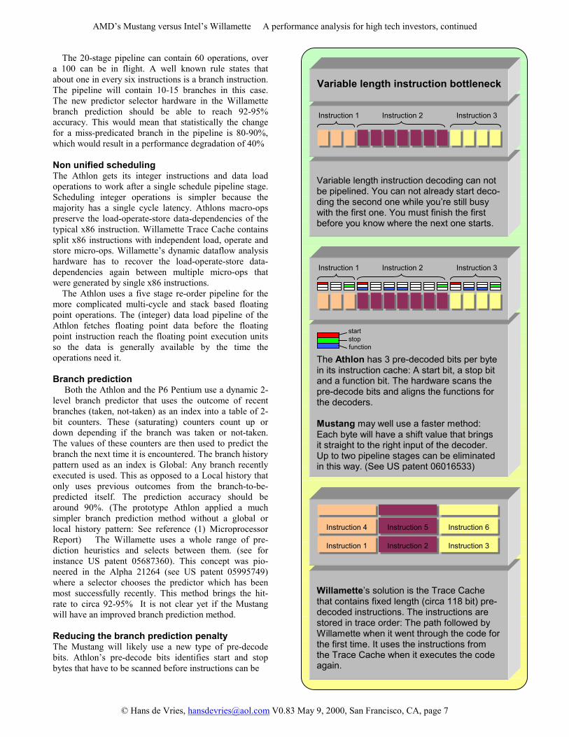
The 20-stage pipeline can contain 60 operations, over a 100 can be in flight. A well known rule states that about one in every six instructions is a branch instruction. The pipeline will contain 10-15 branches in this case. The new predictor selector hardware in the Willamette branch prediction should be able to reach 92-95% accuracy. This would mean that statistically the change for a miss-predicated branch in the pipeline is 80-90%, which would result in a performance degradation of 40% Non unified scheduling The Athlon gets its integer instructions and data load operations to work after a single schedule pipeline stage. Scheduling integer operations is simpler because the majority has a single cycle latency. Athlons macro-ops preserve the load-operate-store data-dependencies of the typical x86 instruction. Willamette Trace Cache contains split x86 instructions with independent load, operate and store micro-ops. Willamette�s dynamic dataflow analysis hardware has to recover the load-operate-store data-dependencies again between multiple micro-ops that were generated by single x86 instructions. The Athlon uses a five stage re-order pipeline for the more complicated multi-cycle and stack based floating point operations. The (integer) data load pipeline of the Athlon fetches floating point data before the floating point instruction reach the floating point execution units so the data is generally available by the time the operations need it. Branch prediction Both the Athlon and the P6 Pentium use a dynamic 2-level branch predictor that uses the outcome of recent branches (taken, not-taken) as an index into a table of 2-bit counters. These (saturating) counters count up or down depending if the branch was taken or not-taken. The values of these counters are then used to predict the branch the next time it is encountered. The branch history pattern used as an index is Global: Any branch recently executed is used. This as opposed to a Local history that only uses previous outcomes from the branch-to-be-predicted itself. The prediction accuracy should be around 90%. (The prototype Athlon applied a much simpler branch prediction method without a global or local history pattern: See reference (1) Microprocessor Report) The Willamette uses a whole range of pre-diction heuristics and selects between them. (see for instance US patent 05687360). This concept was pio-neered in the Alpha 21264 (see US patent 05995749) where a selector chooses the predictor which has been most successfully recently. This method brings the hit-rate to circa 92-95% It is not clear yet if the Mustang will have an improved branch prediction method. Reducing the branch prediction penalty The Mustang will likely use a new type of pre-decode bits. Athlon�s pre-decode bits identifies start and stop bytes that have to be scanned before instructions can be
Variable length instruction decoding can not be pipelined. You can not already start deco-ding the second one while you�re still busy with the first one. You must finish the first before you know where the next one starts.
Variable length instruction bottleneck
The Athlon has 3 pre-decoded bits per byte in its instruction cache: A start bit, a stop bit and a function bit. The hardware scans the pre-decode bits and aligns the functions for the decoders. Mustang may well use a faster method: Each byte will have a shift value that brings it straight to the right input of the decoder. Up to two pipeline stages can be eliminated in this way. (See US patent 06016533)
Instruction 1 Instruction 2 Instruction 3
Instruction 1 Instruction 2 Instruction 3
start stop function
Willamette�s solution is the Trace Cache that contains fixed length (circa 118 bit) pre-decoded instructions. The instructions are stored in trace order: The path followed by Willamette when it went through the code for the first time. It uses the instructions from the Trace Cache when it executes the code again.
Instruction 1 Instruction 2 Instruction 3
Instruction 4 Instruction 5 Instruction 6

AMD�s Mustang versus Intel�s Willamette A performance analysis for high tech investors, continued
© Hans de Vries, [email protected] V0.83 May 9, 2000, San Francisco, CA, page 8
Execute FP6
Execute FP5
Execute FP4
Execute FP3
Execute FP2
Execute FP1
ATHLON WILLAMETTE
Level 1 Cache miss after
branch miss-prediction loop
6 floating point stages?
Estimated pre-fetching
and pre-decoding
front-end
ATHLON, WILLAMETTELEVEL 2 MODES:
BLANK OR INVALID INSTRUCTION CACHE
CONTENTS
Trace Cachemiss after
branch miss-prediction loop
Coppermine front-end pipeline re-used?
Write instructions to Trace Cache
INSTRUCTIONFETCH
INSTRUCTIONDECODE
INSTRUC.EXECUTE
INSTRUCTIONREORDER
floating point data
integer data
Execute FP4
Execute FP3
Execute FP2
Execute FP1
Register File
Schedule
Schedule
Rename Reg
Remap Stack
Data Cache
Data Cache
Execute Int. and AGU
Schedule
Instr. Decode
Early Decode
Align 2
Align 1
scan
Pre-decode
Pre-decode
Level 2 Cache Acces
Level 2 Cache Acces
Level 2 Cache Acces
(Pre-) Fetch
Data Cache
Drive
Data Cache
AGU
Branch Check
Flags
Execute Int.
FP registers
FP registers
Integer Register File
Integer Register File
Dispatch
Dispatch
Schedulers
Schedulers
Schedulers
Queues
Rename
Rename
Allocate
Drive
X86 decode, Micro-op
generation
X86 decode, Micro-op
generation
X86 decode, Micro-op
generation
Level 2 Cache Access
Level 2 Cache Access
Branch Target Buffer
Trace CacheDecoded
Instr. Fetch
Trace Cachenext
Instr. Pointer
Two stages eliminated on the Mustang?

Mustang versus Willamette A performance analysis for high tech investors, continued
© Hans de Vries, [email protected] V0.83 May 9, 2000, San Francisco, CA, page 9
aligned for the Instruction decoders. US patent 06016533 describes pre-decode bits which include a shift value per byte which brings the various bytes of an instruction directly to the right inputs of the decoders. This would eliminate the scan stage and possibly one of the align stages. This would bring the branch penalty miss prediction down to > 8 cycles. If fetching data early from memory, ahead of the operations, is important then the Mustang can start loading data six cycles after the instruction cache access with two load ports in parallel. The Willamette in contrast needs fifteen cycles from the trace-cache access to the single load port data-cache before it can start loading. Branches based on floating point flags The floating point compare instructions introduced in the P6 Pentium generate the flags directly from floating point numbers, reducing the delay to detect a branch miss prediction. The branch miss prediction penalty in the Athlon is 4 cycles more for �floating-point� flag depen-dent branches because of the four cycle longer floating point re-order pipeline. In this case it is no longer the integer pipeline that determines the branch miss-predication delay but the floating point pipeline. Floating point data from memory is generally available before the floating point compare in the Athlon, reducing the total penalty compared with that of the Willamette where a load will stall a floating point operation that needs the data by three cycles. Eliminating branches. The conditional moves, which were also introduced by the P6 Pentium can sometimes replace the harder to predict conditional branches which are the result of if-then-else statements. The pipelines in �level 2� mode The level 2 cache has to be accessed in case of instructing cache / trace cache misses. The Athlon has to pre-decode the instructions before it writes them into the instruction cache while Willamette has to decode x86 into micro-ops that are stored in the trace cache. It is rumored and likely that Intel has re-used the P6 instruction decoder front-end in the Willamette where it now sits between the L2 cache and the trace cache. It would run at half the speed (see US patent 05828868). Variable length instruction decoding The decoding of variable length instructions can not be pipelined. It is not possible to start decoding future instruction while the previous instructions are still busy being decoded. This is because the start locations depend on the length of the preceding instructions. The sole purpose of the Trace Cache and Athlon�s pre-decoding bits is to circumvent this basic bottleneck of the x86 architecture.
Intel mentions that the branch prediction for the front-end and the trace cache are closely coupled. (See US Patent 6055630) This would allow the Willamette to run effectively like a 750 MHz Coppermine when there is no valid instruction data available in the Trace Cache. This is always the case when the Willamette runs for the first time through a piece of code. The trace cache provides the instructions whenever the code is executed for the next time. The trace cache can be kept to a reasonable size because of this high performance fall-back mode. We expect 128 entries x 4 ways = 512 lines of 6 instructions. Each instruction is circa 118 bits resulting in a trace cache of 45.3 kbyte compared to 16 kbyte for the Coppermine instruction cache. The Athlon uses a pre-decoding unit that operates on pre-fetched data from the L2 cache. We have estimated a total of six pipeline stages for this front end for the purpose of our branch-miss-prediction-penalty calcula-tions. If a single 128 bit line from the instruction line cache contains on average five instructions then it will take 6 + (5-1) = 10 cycles before a fully pre-decoded 128 bit line can be delivered to the instruction cache.
Table 4. Branch miss-predict penalties
Mustang Willamette
Integer conditional branch miss-prediction and Instruction cache hit
> 8 cycles
> 20 cycles
Floating point (register) conditional branch miss-prediction and Instruction cache hit
> 12 cycles
> 20 cycles
Floating point (memory) conditional branch miss-prediction and Instruction cache hit
> 12 cycles
> 23 cycles
Integer conditional branch miss-prediction and Instruction cache miss
> 18 cycles
> 28 cycles
Floating point (register) conditional branch miss-prediction and Instruction cache miss
> 22 cycles
> 28 cycles
Floating point (memory) conditional branch miss-prediction and Instruction cache miss
> 22 cycles
> 31 cycles
Instruction cache miss
1..10 cycles
> 1..8 cycles

Mustang versus Willamette A performance analysis for high tech investors, continued
© Hans de Vries, [email protected] V0.83 May 9, 2000, San Francisco, CA, page 10
Estimating the data dependency penalties One of the strongest points of Willamette�s new micro architecture seems to be the very low latencies for integer operations and data-cache load operations. Most performance improvement expectations are based on examples of series of integer instructions, some with access to the data cache. We need a sufficiently accurate model of the ALU and data cache load path to be able to compare the Willamette�s and Athlons integer perfor-mance. Such a model has been developed and is described below: Our model for the data dependency estimations The model described here is consistent with all currently available information. It predicts correctly all examples given by Intel. It also adheres to the rules of circuit design, which define how many logic levels can be implemented within a certain clock period depending on the logic process. Our starting point is a P6 type ALU, which handles the basic integer x86 operations within a single clock cycle. Exceptions are the P6 integer multiply and divide functions which take 4 cycles for the (pipelined) multiply and 12-36 cycles for the (non-pipelined) divide. The multiply is handled by separate hardware. The divide is handled by a sequencer, which may or may not utilize the basic ALU. We can separate the single cycle functions into two categories: (1) The important functions which are abundant in the average program like addition, subtraction, increment, decrement and logical functions like AND, OR XOR and NOT. We would like to see the shift function in this category but the current Willamette does not have an efficient implementation of the shift function. The documentation states that series of adds can be faster than small shifts. (2) The legacy functions, which are hardly ever used and are generally not emitted by C compilers. These include functions like rotate-through-carry, decimal-adjust-AL-after-addition, clear-carry-flag, ascii-adjust-after-subtrac-tion et-cetera. The implicit generation and use of flags is typical for the x86 instruction set. This is reflected in the ALU design that has a flags circuit at the end of the pipeline-stage. This circuit extracts information from the result like parity, sign and zero. The propagation delay of the flag logic consumes about 25% of the total cycle time. It thus reduces the obtainable frequency of the ALU by 25%. The flags are an inherent part of the result data. The flags are kept together with the data in the renamed register until the instruction that generated them is retired. Compilers use the flags only for conditional branches. Modern compilers will emit conditional moves whenever they can do so in order to avoid real branches. The carry is for example used in the 64-bit integer macros of the
compiler but the majority of the data operations in the average program does not need the implicit flags. The ALUs in the Willamette exploits this fact. They can bypass the result of one operation directly to an input of the next one, (before the flags are calculated) This is true for all the functions defined in group 1.
LFU
One �legacy� and two simple ALUs as found in stage 10 of the P6 processing Pipeline: �EXECUTE�
One �legacy� and four simple ALUs as located in our model of Willamette�s stage 17 �EXECUTE� and stage 18 �FLAGS� of the post Trace Cache proc-essing pipeline.
RF0
ALU
RENAMED / REAL REGISTERS and BYPASSES
flags
Legacy Function
Unit
ALU
RF1 flags
RF2 flags
ALU
RF3
ALU
flags
LFU
RF0
ALU
flags
Legacy Function
Unit
RF1 flags
ALU
RENAMED / REAL REGISTERS and BYPASSES
Willamette
P6 Pentium
RF3
Port 0 Port 1
Mustang versus Willamette A performance analysis for high tech investors, continued
© Hans de Vries, [email protected] V0.83 May 9, 2000, San Francisco, CA, page 11
Table 5. Integer ALU data dependency timing
All numbers in clock cycles
Athlon
Willamette
First
operation
Second operation
Second Starts after
Total
latency
Second Starts after
Total
Latency
add/sub
1
2
0.5
1.5
boolean
1
2
1.0
1.5
add/sub
shift/rot
1
2
2.0
4.0
add/sub
1
2
0.5
1.5
boolean
1
2
0.5
1.0
boolean
shift/rot
1
2
2.0
4.0
add/sub
1
2
2.0
3.0
boolean
1
2
2.0
2.5
shift/rot
shift/rot
1
2
2.0
4.0
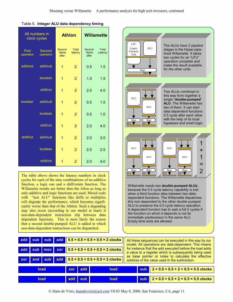
Willamette needs two double-pumped ALUs. because the 0.5 cycle latency capability is lost when a third function slips between two data-dependent functions. The Willamette dispatches this non-dependent to the other double pumped ALU to preserve the 0.5 cycle latency operation. A dependent function has to wait a full 2 cycles if the function on which it depends is not its immediate predecessor in the same ALU. Empty time slots are allowed.
LFU
RF0
ALU
flags
Legacy Function
Unit
The ALUs have 2 pipeline stages in the Hyper-pipe- lined Willamette. It takes two cycles for an �LFU� operation complete and make the result available for the other units
xor and sub add
load xor add load sub
0.5 + 0.5 + 0.5 + 0.5 = 2 clocks
2 + 0.5 + 0.5 + 2 + 0.5 = 5.5 clocks
add sub mov xor 0.5 + 0.5 + 0.5 + 0.5 = 2 clocks
add sub sub add 0.5 + 0.5 + 0.5 + 0.5 = 2 clocks
load add sub load sub 2 + 0.5 + 0.5 + 2 + 0.5 = 5.5 clocks
All these sequences can be executed in this way by ourmodel. All operations are data-dependent. This meansfor instance that the add executed before the load addsa value to a register which is subsequently being usedas base pointer or index to calculate the effectiveaddress of the value used in the subtraction.
RF0flags
ALU
ALU
RF1flags
RF0flags
ALU
ALU
RF1flags
RF2 flags
ALU
ALU
RF3 flags
1+1=2
Two ALUs combined in this way form together a single �double-pumped�ALU. The Willamette has two of them. It can start data dependent functions 0.5 cycle after each other with the help of its local bypasses and smart logic.
The table above shows the latency numbers in clockcycles for each of the nine combinations of an additivefunction, a logic one and a shift/rotate function. TheWillamette results are better then the Atlon as long asonly additive and logic functions are used. Mixed codewith �non ALU� functions like shifts or multiplieswill degrade the performance, which becomes signifi-cantly worse than that of the Athlon. Such a degradingmay also occur (according to our model at least) ifnon-data-dependent instruction slip between datadependent functions. This is most likely the reasonthat a second double-pumped ALU is added to whichnon-data-dependent instructions can be dispatched.

Mustang versus Willamette A performance analysis for high tech investors, continued
© Hans de Vries, [email protected] V0.83 May 9, 2000, San Francisco, CA, page 12
The P6 Pentium III has two integer ALUs. A complex one on port 0 which can handle both the elementary operations and the �legacy� operations. The other ALU on port 1 can only handle the elementary operations: addition, subtraction, logical functions but not the shift. Port 2 is used for the load address generator and port 3 and 4 are used for the store address generator. Willamette has 6 integer ports, ports 0 to 3 are used for the four ALUs and port 5 and 6 are used for the load and store address generator. The very long re-order pipeline for the integer execution unit suggest that Integer and Floating point operation are handled together like on the P6 Pentium and not separatly like on the Athlon. Where the two exactly split is not clear from the drawings. It seems that there are separate ports for integer and floating point units from separated register files. Integer Ports 0 and 1 are connected to one double pumped ALU while ports 2 and 3 are connected to the other. Two operations per cycle can be isued to these units. The load and store AGUs accept one operation per cycle. Pipelining the ALUs to two stages allows the frequency to be increased but doubles all the latencies in data-dependent code. This would have made the Willamette literally slower than a 1 GHz P6 Pentium in many cases. The reason behind the double-pumped ALU design must have been to reduce the latencies back again and if possible improve them over the P6 Pentium. The Data Cache has been kept within two cycles. This is probably the most important feature although it also limits the clock frequency. The AGU address adder allows the addition / subtraction of extra data in parallel with the normal address calculation according to our model. This is an improvement in the given example but the vast majority of loads does not use such a complex address calculation. The x86 address adder can already combine a base pointer, a shifted index and an immediate value without any ALU intervention. This is enough to handle most memory accesses. The ½ cycle latency feature improves the data-dependency characteristics of the Willamette well beyond the P6 Pentiums single cycle ALUs. It works however only for additive and logical instructions and looses much of its advantages if code is mixed with shifts, multiplies or if data independent operations slip between data-dependent ones. The performance stays memory access limited because of the single read port of the data cache. Our model shows that the ½ cycle latency capability is lost if a non-dependent instruction slips between two data dependent instructions. The latency will become a full 2 cycles in this case. A second double pumped ALU is needed to which the non-dependent instruction can be dispatched without disrupting the ½ cycle latency capability. The degradation caused by mixing code with shifts and multiplies can also be considerable. Adding for instance a single shr (shift right) function to Glenn Hinton example increases the number of cycles from 2 to 5! (See page 15) It is no wonder that Intel mentions that a series of adds can be faster than a small shift.
These two ALUs are 100% equivalent. There is no way to determine on the outside which of the two is inside! The second one may also be the ALU used in the Willamette. The first one has less propagation delay and is saver to implement.Glenn Hinton sheets show four ALUs working as two double pumped ALU�s. So we think the first version comes closest to the implementation.
RF0 flags
ALU
ALU
RF1 flags
eq.
RF0 flags
ALU
RF1 flags
Register loads on positive clock edge Register loads on negative clock edge Register loads on both clock edges
Both sides of the double pumped ALU have one basically empty slot. These empty slots allow them to work in their skewed �double pumped� fashion. The timing budget is thus used for 75%. This is a confirmation that the Willamette is designed for 50% higher speeds then the P6. (not 100%) 1.5 GHz against 1 GHz for the Pentium III: 4 (slots) x 1 GHz x 75% = 3 GHz ALU operation
RF0 flags
ALU
ALU
RF1 flags
Empty slot
Filled slot
Filled slot
Filled slot Empty slot
Filled slot
Filled slot
2:1 mux
Filled slot

Mustang versus Willamette A performance analysis for high tech investors, continued
© Hans de Vries, [email protected] V0.83 May 9, 2000, San Francisco, CA, page 13
physical address == physical tag
Our model: Willamette�s �Double- pumped" 3 GHz ALU Including the load- address generator and the read port of the data cache
�Incomplete Address� Decoder
carry select word-lines
Data
Cache Tags
(4-way)
virtual and physical
�Incomplete Address� Decoder
carry select word-lines
Data CacheRam
(4-way)
select between 4-ways
positive edge register
positive edge register
negative edge register
4:1 mux
Full 32 bitAddressAdder
EffectiveAddress( virtual )
negative edge register
6:2 CSA
positive edge register
A0 B0 L0
4:1 mux 4:1 mux
positive edge register
Flags Logic
positive edge register
TranslationLook-aside
Buffer
Effective Address
( physical )
4, 4 and 5 bit address adders
partly completed address
positive edge register
carries
DC
SEGMENT BASE DISPLACE-
INDEX MENT
add sub mov xor
load xor add load sub
0.5 + 0.5 + 0.5 + 0.5 = 2 clocks
2 + 0.5 + 0.5 + 2 + 0.5 = 5.5 clocks
Data Cache 2
Data Cache 1
AGU
Flags
Execute Int.
4x virtual tag
compare
select physical
tag
RENAMED REGISTERS, REAL REGISTERS and BYPASSES ( Provides four values for one single double-pumped ALU )
4xPT
L0
3:2 CSA Boolean function.
32 bit Adder
A0 B0
R0 ALU 0
LOADAGU
Two ALUs work as one
�double- pumped�
3 GHz ALU
DC R0 B1 L1 A1 �0�
L1
3:2 CSABoolean function.
32 bit Adder
A1 B1
R1ALU 1
R1 B0 L0A0�0�
R1 R1
Local Bypasses:Colored dots
are connected
�0�
Cache Hit
Flags Logic
RF0 RF1
4xVT VA
FLAGS 0
FLAGS 1resolve CF,OF
Mustang versus Willamette A performance analysis for high tech investors, continued
© Hans de Vries, [email protected] V0.83 May 9, 2000, San Francisco, CA, page 14
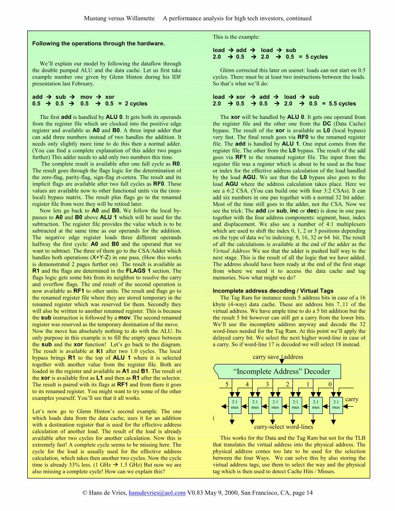
Following the operations through the hardware. We�ll explain our model by following the dataflow throughthe double pumped ALU and the data cache. Let us first takeexample number one given by Glenn Hinton during his IDFpresentation last February. add ���� sub ���� mov ���� xor 0.5 ���� 0.5 ���� 0.5 ���� 0.5 = 2 cycles The first add is handled by ALU 0. It gets both its operandsfrom the register file which are clocked into the positive edgeregister and available as A0 and B0. A three input adder thatcan add three numbers instead of two handles the addition. Itneeds only slightly more time to do this then a normal adder.(You can find a complete explanation of this adder two pagesfurther) This adder needs to add only two numbers this time. The complete result is available after one full cycle as R0. The result goes through the flags logic for the determination ofthe zero-flag, parity-flag, sign-flag et-cetera. The result and itsimplicit flags are available after two full cycles as RF0. These values are available now to other functional units via the (non-local) bypass matrix. The result plus flags go to the renamedregister file from were they will be retired later. Now lets go back to A0 and B0. We follow the local by-passes to A0 and B0 above ALU 1 which will be used for thesubtraction. The register file provides the value which is to besubtracted at the same time as our operands for the addition.The negative edge register loads three different operandshalfway the first cycle: A0 and B0 and the operand that wewant to subtract. The three of them go to the CSA/Adder whichhandles both operations (X+Y-Z) in one pass. (How this worksis demonstrated 2 pages further on) The result is available asR1 and the flags are determined in the FLAGS 1 section. Theflags logic gets some bits from its neighbor to resolve the carryand overflow flags. The end result of the second operation isnow available as RF1 to other units. The result and flags go tothe renamed register file where they are stored temporary in the renamed register which was reserved for them. Secondly theywill also be written to another renamed register. This is becausethe sub instruction is followed by a mov. The second renamedregister was reserved as the temporary destination of the move.Now the move has absolutely nothing to do with the ALU. Itsonly purpose in this example is to fill the empty space betweenthe sub and the xor function! Let�s go back to the diagram.The result is available at R1 after two 1.0 cycles. The localbypass brings R1 to the top of ALU 1 where it is selectedtogether with another value from the register file. Both areloaded in the register and available as A1 and B1. The result ofthe xor is available first as L1 and then as R1 after the selector.The result is paired with its flags at RF1 and from there it goesto its renamed register. You might want to try some of the otherexamples yourself. You�ll see that it all works. Let�s now go to Glenn Hinton�s second example. The onewhich loads data from the data cache, uses it for an additionwith a destination register that is used for the effective addresscalculation of another load. The result of the load is alreadyavailable after two cycles for another calculation. Now this isextremely fast! A complete cycle seems to be missing here. The cycle for the load is usually used for the effective addresscalculation, which takes then another two cycles. Now the cycletime is already 33% less. (1 GHz � 1.5 GHz) But now we arealso missing a complete cycle! How can we explain this?
This is the example: load ���� add ���� load ���� sub 2.0 ���� 0.5 ���� 2.0 ���� 0.5 = 5 cycles Glenn corrected this later on usenet: loads can not start on 0.5
cycles. There must be at least two instructions between the loads.So that�s what we�ll do: load ���� xor ���� add ���� load ���� sub 2.0 ���� 0.5 ���� 0.5 ���� 2.0 ���� 0.5 = 5.5 cycles The xor will be handled by ALU 0. It gets one operand fromthe register file and the other one from the DC (Data Cache)bypass. The result of the xor is available as L0 (local bypass)very fast. The final result goes via RF0 to the renamed registerfile. The add is handled by ALU 1. One input comes from theregister file. The other from the L0 bypass. The result of the addgoes via RF1 to the renamed register file. The input from theregister file was a register which is about to be used as the baseor index for the effective address calculation of the load handledby the load AGU. We see that the L0 bypass also goes to theload AGU where the address calculation takes place. Here wesee a 6:2 CSA. (You can build one with four 3:2 CSAs). It canadd six numbers in one pas together with a normal 32 bit adder.Most of the time still goes to the adder, not the CSA. Now wesee the trick: The add (or sub, inc or dec) is done in one passtogether with the four address components: segment, base, indexand displacement. We also see a number of 4:1 multiplexerswhich are used to shift the index 0, 1, 2 or 3 positions dependingon the type of data we�re indexing: 8, 16, 32 or 64 bit. The resultof all the calculations is available at the end of the adder as theVirtual Address We see that the adder is pushed half way to thenext stage. This is the result of all the logic that we have added.The address should have been ready at the end of the first stagefrom where we need it to access the data cache and tagmemories. Now what might we do? Incomplete address decoding / Virtual Tags The Tag Ram for instance needs 5 address bits in case of a 16
kbyte (4-way) data cache. These are address bits 7..11 of thevirtual address. We have ample time to do a 5 bit addition but thethe result 5 bit however can still get a carry from the lower bits.We�ll use the incomplete address anyway and decode the 32word-lines needed for the Tag Ram. At this point we�ll apply thedelayed carry bit. We select the next higher word-line in case ofa carry. So if word-line 17 is decoded we will select 18 instead. ( This works for the Data and the Tag Ram but not for the TLB
that translates the virtual address into the physical address. Thephysical address comes too late to be used for the selectionbetween the four Ways. We can solve this by also storing thevirtual address tags, use them to select the way and the physicaltag which is then used to detect Cache Hits / Misses.
carry-select word-lines
carry
0
2:1 mux
2:1 mux
2:1 mux
2:1 mux
2:1 mux
2:1 mux
1 3 2 5 4
carry save address
�Incomplete Address� Decoder

Mustang versus Willamette A performance analysis for high tech investors, continued
© Hans de Vries, [email protected] V0.83 May 9, 2000, San Francisco, CA, page 15
Floating Point / MMX / SSE2 / 3Dnow! We expect from Willamettes Basic Architecture Manual that the SSE2 units and Floating point units and jump execution units are also connected to ports 0..3. We have no information how. It seems that the Willamette has a united ROB (Re-Order Buffer) for integer and floating point operations just like the P6 Pentium. The manual states that �A few units do accept an operation every other cycle� No information is available which units but it is posible that these units are the SSE2 floating point add and multiply units. These 128 bit functions are executed in the P6 by two 64 bit operations, one after the other, so that only half of the floating point hardware is needed. This might stil be the case in the Willamette. Intel does not make any statement about the number of Gigaflops Willamette�s SSE2 unit�s achieve. One would expect Intel�s Marketing to add such a number to the list of Willamette�s features if the performance per clock cycle was realy doubled compared to the Pentium III.
If Willemette still uses two 64 bit operations for one 128 bit operation then we can conclude that the floating point, MMX/XMM and SSE/3Dnow! Performance of the Mustang and the Willamette are simular The Willamette can issue 6 operations per cycle in total. Two of them are the load and the store. The Athlon can issue 6 integer operations per cycle: 3 ALU operations and 3 load or load/store operations. It can further issue 3 Floating Point operations per cycle: - One FP multiply /MMX alu,multiply / 3Dnow! multiply - One FP add / MMX add / 3Dnow! add - One FP/MMX/3Dnow!/ Store operation The FP/MMX/3Dnow! Load operations are handled by the short integer pipeline which asures that data is mostly available on time or before it is needed as long as there are no L1 data cache misses.
xor add load sub
xor flags To renamed register file
add flags To renamed register file
AGU load To renamed register file
sub flags
5.5 clocks
xor add AGU load
xor
add
AGU load To renamed register file
To renamed register file Athlon
load
load
sub
sub To renamed register file
Willamette
8 clocks
add sub mov xor
To renamed register file add
sub
xor
flags
flags
flags To renamed register file
add
sub
xor To renamed register file
To renamed register file
To renamed register file
add sub xor 4 clocks
shr stall
shr flags
shr
shr
5 clocks
Athlon
To renamed register file
Willamette non-parallel data-dependent code sequences ALU 0
ALU 1
ALU 1
�LFU�
ALU 0
ALU 1
AGU
ALU 0
Final data to renamed
register file
Final data to renamed
register file
Final data to renamed
register file Final data to
renamed register file

Mustang versus Willamette A performance analysis for high tech investors, continued
© Hans de Vries, [email protected] V0.83 May 9, 2000, San Francisco, CA, page 16
L
3:2 CSA Boolean function.
32 bit Adder
A B
R
RF0 flags
ALU
ALU
RF1 flags
32 bit Adder
3:2 CSA X [31:0] Y [31:0] Z [31:0]
A [31:0] B [31:0]
CSA
X3 Y3 Z3
CSA
X2 Y2 Z2
CSA
X1 Y1 Z1
CSA
X0 Y0 Z0
CSA
X4 Y4 Z4
CSA
X5 Y5 Z5
CSA
X6 Y6 Z6
B0 A0 B2 A2 B1 A1 B3 A3 B6 A6 B5 A5 B4 A4
1st = INC or SUB
2nd = INC or SUB carry32 bit Adder
Z7
B7
Truth table for all 16 combinations of ADD, SUB, INC and DEC
first op second op
X Y Z
ADD ADD
X+Y+Z
ADD SUB
X+Y-Z
SUB ADD
X-Y+Z
SUB SUB
X-Y-Z
INC ADD
X+1+Z
INC SUB
X+1-Z
DEC ADD
X-1+Z
DEC SUB
X-1-Z
ADD INC
X+Y+1
SUB INC
X-Y+1
ADD DEC
X+Y-1
SUB DEC
X-Y-1
0 0 00 0 10 1 00 1 11 0 01 0 11 1 01 1 1
0 00 10 11 00 11 01 01 1
0 10 01 00 11 00 11 11 0
0 11 00 00 11 01 10 11 0
1 00 10 10 01 11 01 00 1
0 00 10 00 10 11 00 11 0
0 10 00 10 01 00 11 00 1
0 11 00 11 01 01 11 01 1
1 00 11 00 11 11 01 11 0
0 00 00 10 10 10 11 01 0
0 10 10 00 01 01 00 10 1
0 10 11 01 01 01 01 11 1
1 01 00 10 11 11 11 01 0
Data Cache 2
Execute FP4
Execute FP3
Execute FP2
Execute FP1
Drive
Data Cache 1
AGU
Branch Check
Flags
Execute Int.
Register File
SUB ADD
X-Y+Z
B1 A00 11 00 00 11 01 10 11 0
X0 Y0 Z0
B1
A0
Dual 8:1
multi plexer
Any combination of ADD, SUB, INC and DEC can be executed in one pass by the combination of this extended 3:2 CSA and a 32 bit adder.

Mustang versus Willamette A performance analysis for high tech investors, continued
© Hans de Vries, [email protected] V0.83 May 9, 2000, San Francisco, CA, page 17
Data dependent
operations (All numbers in nano seconds)
2.0 GHz
�single-pumped� ALU
1.5 GHz Willamette
1st op
2nd op
2nd
starts after
2nd
result ready
2nd
result output
2nd
starts after
2nd
result ready
2nd
result output
add/sub
0
1
1
0.33
1.00
1.33
Boolean Ex. AND
0
1
1
0.66
1.00
2.00
add/sub
shift
1
2
2
1.33
2.66
2.66
add/sub
0
1
1
0.33
1.00
1.33
boolean
0
1
1
0.33
0.66
1.33
boolean
shift
0
1
1
1.33
2.66
2.66
add/sub
1
2
2
1.33
2.00
2.66
boolean
0
1
1
1.33
1.66
2.66
shift
shift
1
2
1
1.33
2.66
2.66
positive edge register
A0 B0
RF0
B1 A1
RF1ALU 0
B0A0A1 B1
3:2 CSA
32 bit Adder
32 bitBarrelshifter
Flagslogic
3:2 CSA
32 bit Adder
32 bit Barrel shifter
Flags logic
positive edge register positive edge register
positive edge register
ALU 1
RENAMED / REAL REGISTERS and BYPASSES
example ALU for a 2.0 GHz processor (at 180 nm)
This example ALU shows that Willamette�s double-pumped ALU is not yet the end station of ALU design. It achieves a higher frequency and has better latency characteristics for most data-dependent combinations. It is a more �conservative� design in this sense that it doesn�t need negative edge-clocked flip-flops. It occupies two pipeline stages just like Willamette�s ALU. The most notable differences: The CSA function is also used for two-input and triple-input Boolean functions. See the examples below: One input is routed unmodified to the A-output if the result of a two input Boolean function has to be combined with an additive or a shift function. The second improvement is the inclusion of the shift and rotate functions. The third improvement is the parallel flags logic. The flags are not calculated after the end result is known but are calculated in parallel and arrive with the end result at the same time. The longest path of the x86 flags is the zero-after-additive-function path. It is most likely that the current Athlon already contains parallel flag logic. Just have a look a US patent number 05862065. The trick is to determine that A+B=0 before you know what A+B is. All zero flag detection tricks are in fact based on the detection of X+Y=0xffff This result can only occur if there is not a single carry during the addition. An adder without carry logic is the same as an XOR function thus: X+Y=0xffff means that X^Y=0xffff. The simplest way to here is to say (A-1)^B=0xffff. A decrementer is already much faster then an adder. AMD�s patent manages however to circumvent the decrement with a smart trick. The fourth improvement is the Boolean function after the additive and shift functions like (A+B)^C. Can you do parallel zero detection for these functions as well? Yes, most are quit simple except the AND which is harder to crack. (A+B) ^ C = 0 � A+B-C = 0 � use the 3:2 CSA! (A+B) | C = 0 � A+B = 0 and C = 0, et-cetera.
2:1 mux 2:1 mux
Boolean 2Boolean 2
AND OR
X&Y|Z
Bn An0 01 00 01 00 01 01 01 0
Xn Yn Zn
Bn
An
Dual8:1
multi plexer
XOR ADD
(X^Y)+Z
Bn An0 00 11 01 11 01 10 00 1

Mustang versus Willamette A performance analysis for high tech investors, continued
© Hans de Vries, [email protected] V0.83 May 9, 2000, San Francisco, CA, page 18
Conclusions: Clock Frequency The very long pipeline of the Willamette is no guarantee that it can reach much higher clock frequencies than currently presented. The pipeline is partly so long because many stages are allocated to a unified re-order pipeline which handles both integer and stack based floating-point operations. A basic 32 bit ALU function like an addition still fits within a single stage like in the Athlon or the P6. The Level 1 data cache also uses basically the same two stages as the Athlon and the P6. It is not unlikely that AMD can decrease the frequency gap (at similar process) with incremental pipeline improvements when it moves to subsequent processor generations. AMD seems to have a process advantage over Intel in its brand new fab 30 in Dresden for dual-damascene inlaid copper production and may move to 130 nm production already at the end of the year after an initial introduction of the Mustang at 150 nm. This would allow the Mustang to run at equal or maybe even higher frequencies as the Willamette at least until the second half of 2001 when Intel�s 130 nm copper process gets rolling after a major transformation of its production lines. Performance per cycle. It is not that easy to determine the performance of processors that have yet to be disclosed in some detail. Hereby the major conclusions from this document provided that the models we have developed are close enough to reality: Willamette The strongest point is the ALU that manages to offset the disadvantages of going from a single cycle ALU to a two stage ALU/flags pipeline. Its performance for data-dependent additive and logic functions is even signifi-cantly better than that of a single cycle ALU. It works only for additive and logical instruction however and looses much of its advantages if code is mixed with shifts, multiplies or if data independent operations slip between data-dependent ones. The performance stays memory access limited because of the single read port of the data cache. Willamette�s weakest point is probably the very long pipeline, which is very susceptible for branch-miss predictions. The branch prediction on the Willamette is improved from the two-level adaptive prediction of the P6 Pentium to a technique similar to a technique introduced by the Compaq Alpha 21264 in 1996: A Predictor Selector chooses the most successful predictor for a particular branch from a whole range of predictors. The improved branch prediction hardware in the Willamette is however unlikely to offset the much longer pipeline. The unified instruction re-order pipeline has 12 cycles. (Compared to an integer re-order pipe of only 1½ stage for the Athlon). This long pipeline also has to handle the loads and stores for both integer and floating point operations. We do predict an integer
performance improvement over the P6 Pentium in code specially written and compiled for the Willamette. Most existing code will probably suffer too much from branch miss-predictions and will show a lower performance per cycle than the P6 Coppermine. This might however be an acceptable offer for a 50% increase in frequency. Mustang The total on-chip cache (L1+L2) tripled from 128k for the Athlon to 384k for Thunderbird with a remarkable performance improvement. It will triple again for the Mustang. The Mustang will have up to 1Mb of L2 cache. The memory sub-system is by far the most important performance factor in processors above 1 GHz. The Mustang can include much more cache on die because of its smaller core size, its process technology: Copper and local tungsten interconnect and its process dimensions: 150-130 nm versus 180-150 nm for the Willamette. The improved pre-decoding bits in the instruction code may eliminate up to two complete pipeline stages: The scan stage and (not unlikely) one align stage, resulting in a reduced branch miss-prediction penalty. (US patent 05987235). An improved branch prediction method for the Mustang, similar to that of the Alpha 21264 or the Willamette would be highly desirable. There is no direct indication for this yet. The most we can say is that AMD is taking this subject very seriously. It improved the Athlon's prediction hardware significantly for the final production version. The prototype Athlons used a much simpler branch prediction. Maybe something like this will happen again for the Mustang. AMD is well aware of the method used by the Alpha 21264. All recently issued AMD patents concerning branch prediction refer to the 21264 patent! (US Patent 05758142). An interesting method which might reduce the on-chip L2 cache latency by potentially 50% is a technique called �Way-predicting� (US patent 06016533) The Mustang�s 1-MB L2 cache is a 16 way unified cache. The L2 cache is normally accessed only after a L1 cache miss. The L2 tags are checked concurrently with the L1 access so that only the L2 �way� which contains the data looked for is accessed after the cache miss. In theory it is possible to access all 16 ways of the L2 cache concurrently with each L1 access. The L2 data would then be immediately available after the L1 miss. This would however need excessive amounts of power dissipation. Way-prediction now tries to predict the L2 way so that only one way needs to be accessed concurrently with the L1 access. I can imagine possible cache line replacement algorithms that might have sufficient predictability. If AMD succeeds here then it can implement a L2 cache with a latency that looks more like a L1 cache. Another recent patent describes a speculative store buffer. A store to memory must normally wait until the outcome of a conditional branch is known. The speculative store buffer delays the actual write but is used for memory loads to the same address. A branch miss-prediction cancels the actual store to memory. While a hit will effectuate the write. (see US Patent 06067616)

Mustang versus Willamette A performance analysis for high tech investors, continued
© Hans de Vries, [email protected] V0.83 May 9, 2000, San Francisco, CA, page 19
Conclusion: Mustang versus Willamette If the conclusions that (a) Willamette would show a somewhat lower performance for existing code as the Coppermine, and (b) The Mustang would show a cycle for cycle improvement over the Thunderbird. Then we must conclude that the performance gap at equal frequency between the current Thunderbird and Coppermine will only grow in the case of the Mustang and Willamette. The basic advantages of the Mustang seems to be that it�s a wider super scalar processor than the Willamette and its short integer instruction pipeline is better resistant against branch miss predictions. If fetching data early from memory ahead of the operations is important then the Mustang can start loading data six cycles after the instruction cache access with two load ports in parallel. The Willamette in contrast needs fifteen cycles from the trace-cache access to the single load port data-cache before it can start loading. Every extra cycle increases the change for a branch miss prediction. The capability to include a much larger on-chip L2 cache on die is the other major advantage that Mustang has over Willamette in the performance race. The semiconductor process advantage of AMD will only be temporary until the second half of 2001. It seems likely however that Mustang still may have the lead at an equal process and thus at a somewhat lower frequency. The only way for Intel to reduce the gap on a short term seems to be to reconsider its server strategy and introduce a version of the Willamette with a large on-chip L2 cache. Even though a large on-chip L2 cache implemented with a 180-nm aluminum process without local interconnect needs a large die size in the 200 mm2 to 300 mm2 range. A large on-chip cache seems currently be reserved for a follow-up for Foster called Gallatin. Foster continues the Xeon tradition with its 256-kbyte on-chip L2 cache and a separate large full speed L3 cache chip in the package. AMD should aim to have a higher frequency micro architecture available before the end of 2001. The year 2002 may well show the race to 100 nm processors based on 193 nm ArF lithography systems. A 100 nm version of Sledgehammer with 2 MB L2 cache would have an approximate die size in the range of 80 to 90 mm2 depending on the extra core logic. It is not so long ago that microprocessor vendors like Intel were scared for smaller and smaller processor dies. They might be left with too much production capacity for the amount of processors needed by the market. Graphics and other system components needed to be integrated to keep the production lines running. Intel�s Timna is a result of such a strategy. Today it looks that smaller processor dies just help to produce the amount of processors required by the ever-increasing PC market fueled by the Internet. That the market will expand seems to be certain. This (technical) performance analysis may help to get an idea how it will be divided. Hans.
On line references: (1) Athlon in depth article in Micro Processor Report: http://chipanalyst.com/pc_processors/articles/v12/121401.pdf (2) Athlon presentations at the ISSCC �99 http://www.sscs.org/isscc/1999/digest/Monday.htm#5.4 and http://www.sscs.org/isscc/1999/digest/Monday.htm#5.5 (3) Athlon optimization guide http://www.amd.com/products/cpg/athlon/techdocs/pdf/22007.pdf (4) K6: instruction predecode bits patent http://www.patents.ibm.com/details?&pn10=US05689672 (5) Athlon: instruction pre-decode patents http://www.patents.ibm.com/details?pn=US06049863__ (6) Mustang(?): instruction pre-decode patent http://www.patents.ibm.com/details?pn=US05987235__ (7) Mustang(?): I cache with branch selectors patent http://www.patents.ibm.com/details?pn=US05995749__ (8) Mustang(?): Way prediction for L2 cache http://www.patents.ibm.com/details?pn=US06016533__ (9) Mustang(?): Speculative Store Buffer http://www.patents.ibm.com/details?pn=US06067616__ (10) Sledgehammer(?) 32 64-bit register file patent http://www.patents.ibm.com/details?pn=US06014739__ (11) Athlon: parallel zero flag patent http://www.patents.ibm.com/details?pn=US05862065__ (12) Athlon: flag renaming patent http://www.patents.ibm.com/details?pn=US05805853__ (13) AMD: effective and intermediate address patent http://www.patents.ibm.com/details?pn=US05583806__ (14) Intel: copy EXACTLY! Strategy http://developer.intel.com/technology/itj/q41998/articles/art_2.htm (15) Willamette presentation at IDF 2000 ftp://download.intel.com/ial/home/sp/idf/dtps01_ps.pdf (16) Willamette�s manuals http://developer.intel.com/design/processor/future/manuals/ (17) Willamette Trace Cache patent http://www.patents.ibm.com/details?&pn=US06018786__ (18)Willamette: core units running on (3) different clocks http://www.patents.ibm.com/details?pn=US05828868__ (19)Willamette: branch prediction maintenance http://www.patents.ibm.com/details?pn=US06055630__ (20) Willamette: multiple heuristics branch prediction http://www.patents.ibm.com/details?&pn10=US05687360 (21) Intel: effective and linear address calculation patent http://www.patents.ibm.com/details?pn=US05625582__ (22) Intel: flag renaming patent: http://www.patents.ibm.com/details?pn=US06047369__ (23) Intel: AGU (Address Generator Unit) Patent: http://www.patents.ibm.com/details?pn=US05590297__ (24) Intel: Pentium III Implementation tradeoffs http://developer.intel.com/technology/itj/Q21999/PDF/impliment.pdf (25) Intel: A 2 MByte Pipeline-Burst L2 Cache SRAM http://www.sscs.org/isscc/1999/digest/Tuesday.htm#11.6 (26) Motorola Copper 1 MegaByte L2 SRAM http://www.chipworks.com//Reports/Flyers/Mot8MSRAM.htm http://devel.penton.com/ed/Pages/magpages/june2298/digdes/0622de1.htm (27) Andreas Kaiser: Athlons branch prediction. http://www.s.netic.de/ak/k7doc.pdf
The author.