Embed Size (px)
Citation preview
Advanced Micro Devices
AMD SB820M Southbridge Databook
Publication #
47283 Revision: 2.10
Issue Date: Dec 2010
47283 Rev. 2.10 Dec 2010 AMD SB820M Southbridge Databook
© 2010 Advanced Micro Devices, Inc. All rights reserved.
The contents of this document are provided in connection with Advanced Micro Devices, Inc. (“AMD”) products. AMD makes no representations or warranties with respect to the accuracy or completeness of the contents of this publication and reserves the right to make changes to specifications and product descriptions at any time without notice. The information contained herein may be of a preliminary or advance nature and is subject to change without notice. No license, whether express, implied, arising by estoppel, or otherwise, to any intellectual property rights are granted by this publication. Except as set forth in AMD’s Standard Terms and Conditions of Sale, AMD assumes no liability whatsoever, and disclaims any express or implied warranty, relating to its products including, but not limited to, the implied warranty of merchantability, fitness for a particular purpose, or infringement of any intellectual property right.
AMD’s products are not designed, intended, authorized or warranted for use as components in systems intended for surgical implant into the body, or in other applications intended to support or sustain life, or in any other application in which the failure of AMD’s product could create a situation where personal injury, death, or severe property or environmental damage may occur. AMD reserves the right to discontinue or make changes to its products at any time without notice.
Trademarks AMD, the AMD Arrow logo, and combinations thereof are trademarks of Advanced Micro Devices, Inc.
Microsoft is a registered trademark of Microsoft Corporation.
PCI Express and PCIe are registered trademarks of PCI-SIG.
Other product names used in this publication are for identification purposes only and may be trademarks of their respective companies.
47283 Rev. 2.10 Dec 2010 AMD SB820M Southbridge Databook
Contents 3
Contents Chapter 1 Introduction ............................................................................................................ 12
1.1 Features of the SB820M Southbridge .............................................................................. 12
1.2 Part Numbers and Brandings ........................................................................................... 15
1.3 SB820M Southbridge Block Diagram ............................................................................. 18
1.4 Conventions and Notations .............................................................................................. 19
1.4.1 Pin Names ................................................................................................................ 19
1.4.2 Pin Types ................................................................................................................. 19
1.4.3 Numeric Representation ........................................................................................... 19
1.4.4 Register Field ........................................................................................................... 20
1.4.5 Acronyms and Abbreviations .................................................................................. 20
Chapter 2 Functional Description .......................................................................................... 22
2.1 EHCI USB 2.0 and OHCI USB 1.1 Controllers .............................................................. 22
2.1.1 USB Power Management ......................................................................................... 24
2.2 SMI/SCI Generation ........................................................................................................ 26
2.2.1 Event Sources for SCI .............................................................................................. 26
2.2.2 SMI Events............................................................................................................... 27
2.2.3 SMI/SCI Work Flow ................................................................................................ 27
2.3 LPC ISA Bridge ............................................................................................................... 29
2.3.1 LPC Interface Overview .......................................................................................... 29
2.3.2 LPC Module Block Diagram ................................................................................... 31
2.4 Real Time Clock .............................................................................................................. 31
2.4.1 Functional Blocks of RTC ....................................................................................... 31
2.5 Serial ATA Controller ..................................................................................................... 32
2.6 PCI Bridge ....................................................................................................................... 33
2.7 High Definition Audio ..................................................................................................... 34
2.7.1 HD Audio Codec Connections................................................................................. 34
2.8 Clock Generation ............................................................................................................. 34
2.9 Power Management/ACPI ............................................................................................... 36
Chapter 3 Ballout Assignment ................................................................................................ 37
Chapter 4 Pin Descriptions ..................................................................................................... 39
4.1 CPU Interface Pin Descriptions ....................................................................................... 39
47283 Rev. 2.10 Dec 2010 AMD SB820M Southbridge Databook
Contents 4
4.2 LPC Interface Pin Descriptions ....................................................................................... 40
4.3 A-Link Express II Interface Pin Descriptions .................................................................. 40
4.4 General Purpose PCI Express® Ports Interface ................................................................ 41
4.5 PCI Interface (PCI Host Bus and Internal PCI/PCI Bridge) ............................................ 41
4.6 USB Interface .................................................................................................................. 44
4.7 Flash Interface .................................................................................................................. 45
4.8 Serial ATA Interface ........................................................................................................ 46
4.9 HD Audio Interface ......................................................................................................... 47
4.10 Real Time Clock Interface ............................................................................................... 48
4.11 SPI ROM Interface .......................................................................................................... 48
4.12 Power Management Interface .......................................................................................... 49
4.13 SMBus Interface .............................................................................................................. 52
4.14 Reset / Clocks / ATE / JTAG ........................................................................................... 53
4.15 General Purpose I/O and General Event .......................................................................... 58
4.16 Keyboard and PS/2 Controller ......................................................................................... 68
4.17 Gigabit Ethernet Media Access Controller (GbE MAC) ................................................. 69
4.18 Infrared Interface ............................................................................................................. 71
4.19 Power and Ground ........................................................................................................... 71
4.20 Integrated Resistors .......................................................................................................... 73
4.21 Strap Information ............................................................................................................. 74
Chapter 5 Power Sequence and Timing ................................................................................. 79
5.1 Power Sequence ............................................................................................................... 79
5.2 Reset Timing .................................................................................................................... 85
5.2.1 ROMRST# ............................................................................................................... 85
5.2.2 System Reset ............................................................................................................ 86
5.2.3 PCIe® Reset .............................................................................................................. 87
5.3 Power Button Timing ....................................................................................................... 89
5.4 ACPI Timing .................................................................................................................... 90
5.4.1 S-State Timing ......................................................................................................... 90
5.4.2 S4 and S5 Timing..................................................................................................... 92
5.4.3 C-State Timing ......................................................................................................... 93
5.4.4 VID/FID Change Timing ......................................................................................... 95
47283 Rev. 2.10 Dec 2010 AMD SB820M Southbridge Databook
Contents 5
5.4.5 Timing Definitions and Descriptions ....................................................................... 97
5.4.6 Registers for S-State and C-State Timing ................................................................ 99
Chapter 6 Electrical Characteristics .................................................................................... 102
6.1 Absolute Ratings ............................................................................................................ 102
6.2 Functional Operating Range .......................................................................................... 102
6.3 DC Characteristics ......................................................................................................... 102
6.4 RTC Battery Current Consumption ............................................................................... 104
6.5 States of Power Rails during ACPI S1 to S5 States ...................................................... 105
6.6 System Clock Specifications ......................................................................................... 106
6.6.1 System Clock Descriptions .................................................................................... 106
6.6.2 System Clock Input Frequency Specifications ...................................................... 106
6.6.3 System Clock Output AC and DC Specifications.................................................. 106
Chapter 7 Package Information ........................................................................................... 110
7.1 Physical Dimensions ...................................................................................................... 110
7.2 Pressure Specification .................................................................................................... 111
7.3 Thermal Information ...................................................................................................... 111
7.4 Reflow Profile ................................................................................................................ 113
Chapter 8 Testability ............................................................................................................. 115
8.1 XOR Chain Test Mode .................................................................................................. 115
8.2 Test Control Signals ....................................................................................................... 115
8.2.1 Brief Description of an XOR Chain ....................................................................... 117
8.2.2 Description of the SB820M XOR Chain ............................................................... 118
Appendix A Pin Listing ............................................................................................................. 124
47283 Rev. 2.10 Dec 2010 AMD SB820M Southbridge Databook
List of Figures 6
List of Figures Figure 1: SB820M Branding Diagrams for (a) Engineer Sample, (b) Production ASIC A12, (c)
Production ASIC A13 .............................................................................................................. 16
Figure 2. Block Diagram Showing the Internal PCI Devices and Major Function Blocks ............. 18
Figure 3. USB Controllers Block Diagram ...................................................................................... 23
Figure 4. SMI/SCI Logic of the SB820M ........................................................................................ 28
Figure 5. SB820M LPC Bus System ............................................................................................... 29
Figure 6. Block Diagram of LPC Module ....................................................................................... 31
Figure 7. Block Diagram of Internal RTC ....................................................................................... 32
Figure 8. Block Diagram for the SATA Module ............................................................................. 33
Figure 9. HD Audio Codec Connections ......................................................................................... 34
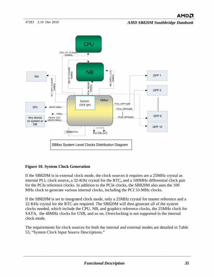
Figure 10. System Clock Generation ............................................................................................... 35
Figure 11: SB820M Ballout Assignment (Left) .............................................................................. 37
Figure 12: SB820M Ballout Assignment (Right) ............................................................................ 38
Figure 13. Straps Capture Timing .................................................................................................... 75
Figure 14. Power-on Sequence (S5 S0 S5) ............................................................................. 79
Figure 15. Power-on Sequence (S3 S0 S3) ............................................................................. 80
Figure 16. Timing for SB PWR_GOOD De-asserted to RSMRST# De-asserted ........................... 84
Figure 17. Measurement for RSMRST# Timing (T2A) .................................................................. 84
Figure 18. LDT_STP# Timing at First power-up, G3G5, or after RSMRST# Assertion ................ 85
Figure 19. ROM Reset Timing ........................................................................................................ 86
Figure 20. System Reset Timing ...................................................................................................... 87
Figure 21. PCIe® Reset Timing ....................................................................................................... 88
Figure 22. Power Button Timing ..................................................................................................... 89
Figure 23. S1-State Timing .............................................................................................................. 90
Figure 24. S3 State Timing .............................................................................................................. 91
Figure 25. S4 and S5 State Timing .................................................................................................. 92
Figure 26. C2/C3-State Timing........................................................................................................ 93
Figure 27. C3 Stutter Mode Timing ................................................................................................. 94
Figure 28. VID/FID Change Timing ............................................................................................... 95
Figure 29. C-State and VID/FID Change Flow Diagram ................................................................ 96
Figure 30. SB820M 23 mm x 23 mm 0.8 mm Pitch 605-FCBGA Package Outline ..................... 110
47283 Rev. 2.10 Dec 2010 AMD SB820M Southbridge Databook
List of Figures 7
Figure 31. RoHS/Lead-Free Solder (SAC305/405 Tin-Silver-Copper) Reflow Profile................ 114
Figure 32. Test Mode Capturing Sequence Timing ....................................................................... 116
Figure 33. A Generic XOR Chain.................................................................................................. 117
Figure 34. On-chip XOR Chain connectivity ................................................................................ 118
47283 Rev. 2.10 Dec 2010 AMD SB820M Southbridge Databook
List of Tables 8
List of Tables Table 1. Pin Type Codes .................................................................................................................. 19
Table 2. Acronyms and Abbreviations ............................................................................................ 20
Table 3. EHCI Support for Power Management States ................................................................... 24
Table 4. EHCI Power State Summary ............................................................................................. 25
Table 5. SCI Event Sources and Mapping into ACPI EventStatus .................................................. 26
Table 6. LPC Cycle List and Data Direction ................................................................................... 30
Table 7. CPU Interface Pin Descriptions ......................................................................................... 39
Table 8. LPC Interface Pin Descriptions ......................................................................................... 40
Table 9. A-Link Express II Interface Pin Descriptions .................................................................... 40
Table 10. General Purpose PCI Express® Ports Interface Pin Descriptions .................................... 41
Table 11. PCI Interface (PCI Host Bus and Internal PCI/PCI Bridge) Pin Description .................. 41
Table 12. USB Interface Pin Descriptions ....................................................................................... 44
Table 13. Flash Interface Pin Descriptions ...................................................................................... 45
Table 14. Serial ATA Interface Pin Descriptions ............................................................................ 46
Table 15. HD Audio Interface Pin Descriptions .............................................................................. 47
Table 16. Real Time Clock Interface ............................................................................................... 48
Table 17. SPI ROM Interface Pin Descriptions ............................................................................... 48
Table 18. Power Management Interface Pin Descriptions ............................................................... 49
Table 19. SMBus Interface Pin Descriptions ................................................................................... 52
Table 20. Reset/Clocks/ATE/JTAG Interface Pin Descriptions ...................................................... 53
Table 21. General Purpose I/O and General Event Pin Descriptions .............................................. 58
Table 22. Keyboard and PS/2 Controller Interface Pin Descriptions .............................................. 69
Table 23. RGMII/MII Pin Descriptions ........................................................................................... 70
Table 24. Gigabit Ethernet PHY Pin Descriptions .......................................................................... 70
Table 25. Infrared Interface Pin Descriptions .................................................................................. 71
Table 26. Power and Ground Pin Descriptions ................................................................................ 72
Table 27. Integrated Resistors .......................................................................................................... 74
Table 28. Standard Straps ................................................................................................................ 75
Table 29. Debug Straps .................................................................................................................... 77
Table 30. Power Sequence Timing .................................................................................................. 81
47283 Rev. 2.10 Dec 2010 AMD SB820M Southbridge Databook
List of Tables 9
Table 31. Power Sequence SB PWRGOOD, NB_PWRGOOD, and System Clock Timing (For Internal Clock Mode Only) ...................................................................................................... 82
Table 32. Power Sequence SB PWRGOOD, NB_PWRGD, and System Clock Timing (For External Clock Mode Only) ..................................................................................................... 82
Table 33. Rom Reset Timing for Various Platform Configurations ................................................ 86
Table 34. System Reset Timing ....................................................................................................... 87
Table 35. PCIe® Reset Timing ......................................................................................................... 88
Table 36. Timing Definitions and Descriptions ............................................................................... 97
Table 37. C3 Enter (Shaded)/Exit .................................................................................................... 98
Table 38. C3 Stutter Enter (Shaded)/Exit ........................................................................................ 98
Table 39. LdtCmd Enter (Shaded)/Exit ........................................................................................... 98
Table 40. S1 Enter (Shaded)/Exit .................................................................................................... 99
Table 41. S3 Enter (Shaded)/Exit .................................................................................................... 99
Table 42. S4 Enter (Shaded)/Exit .................................................................................................... 99
Table 43. Registers for Programming Sx and Cx-State Timing .................................................... 100
Table 44. Recommend Values for Programming Sx and Cx-State Timing ................................... 100
Table 45. DC Characteristics of the GPIO pins. ............................................................................ 102
Table 46. DC Characteristics of the PCI Interface ........................................................................ 102
Table 47. DC Characteristics of the CPU Interface ....................................................................... 103
Table 48. DC Characteristics of RSMRST# .................................................................................. 103
Table 49. DC Characteristics of SBPWRGD ................................................................................ 103
Table 50. DC Characteristics of the LPC Interface ....................................................................... 104
Table 51. RTC Battery Current Consumption (Preliminary Estimates) ........................................ 104
Table 52. States of Power Rails during ACPI S1 to S5 States ...................................................... 105
Table 53. System Clock Input Source Descriptions ...................................................................... 106
Table 54. System Clock Input Frequency Specifications .............................................................. 106
Table 55. NB_DISP_CLKP/N AC Specifications: (Non-Spread Clock) ...................................... 107
Table 56. CPU_HT_CLKP/N AC Specifications .......................................................................... 107
Table 57. 14-MHz/25-MHz/48-MHz Auxiliary Clock AC Specifications: .................................. 108
Table 58. PCI Clock AC Specifications ........................................................................................ 108
Table 59. SB820M 23 mm x 23 mm 0.8 mm Pitch 605-FCBGA Physical Dimensions ............... 110
Table 60. SB820M Thermal Limits ............................................................................................... 111
Table 61. SB820M Thermal Design Power for Different Platform Configurations ...................... 112
47283 Rev. 2.10 Dec 2010 AMD SB820M Southbridge Databook
List of Tables 10
Table 62. Recommended Board Solder Reflow Profile - RoHS/Lead-Free Solder ...................... 113
Table 63. Signals for the Test Controller of the SB820M ............................................................. 115
Table 64. Test Mode Signals ......................................................................................................... 115
Table 65. TEST0 Bit Sequence ...................................................................................................... 116
Table 66. Truth Table for an XOR Chain ...................................................................................... 117
Table 67. List of Pins on the SB820M XOR Chain and the Order of Connection ........................ 118
Table 68. Signals that are not part of the XOR chain .................................................................... 123
Table 69. Pin Listing by Interface .................................................................................................. 124
Table 70. Pin List by Signal Name ................................................................................................ 134
47283 Rev. 2.10 Dec 2010 AMD SB820M Southbridge Databook
Revision History 11
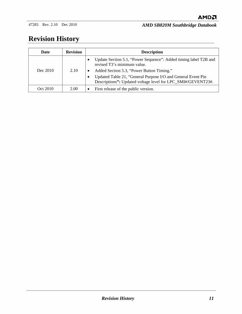
Revision History
Date Revision Description
Dec 2010 2.10
• Update Section 5.1, “Power Sequence”: Added timing label T2B and revised T3’s minimum value.
• Added Section 5.3, “Power Button Timing.” • Updated Table 21, “General Purpose I/O and General Event Pin
Descriptions”: Updated voltage level for LPC_SMI#/GEVENT23#. Oct 2010 2.00 • First release of the public version.
47283 Rev. 2.10 Dec 2010 AMD SB820M Southbridge Databook
Introduction 12
Chapter 1 Introduction
The AMD SB820M Southbridge integrates key I/O, communications, and audio features required in a state-of-the-art PC into a single device. It is specifically designed to operate with AMD’s integrated graphics processors (IGPs) and Northbridges (NBs) in mobile PCs.
1.1 Features of the SB820M Southbridge Processor Interface
Supports AMD mobile processors code-named “Champlain,” and “Geneva.”
A-Link Express II interface to
Northbridges
1-, 2-, or 4-lane A-Link Express II interface
Automatic detection of lane configuration on boot-up
Supports transfer rate of up to 2.5 GT/s per lane.
PCI Express® Controller
Two-lane PCI Express® (PCIe®) 1.x interface, supporting up to two general purpose devices. Supported configurations include:
1x2
2x1
PCI Host Bus Controller
Supports PCI bus at 33MHz
Supports PCI Rev. 2.3 specification
Supports up to 4 bus master devices
Supports 40-bit addressing
Interrupt steering supported for plug-n-play devices
Supports concurrent PCI operations
BIOS/hardware support to hide PCI device
Supports spread spectrum
USB Controllers
4 OHCI and 3 EHCI host controllers to support 14 USB 2.0 ports and 2 dedicated USB 1.1 ports
Supports ACPI S1 ~ S5
Supports USB keyboard/mouse functionality for legacy Operating Systems
USB debug port
Supports individual port disable capability
SMBus Controller
Supports SMBALERT # signal
Interrupt Controller
Supports IOAPIC/X-IO APIC mode for 24 channels of interrupts
Supports 8259 legacy mode for 15 interrupts
47283 2.10 Dec 2010 AMD SB820M Southbridge Databook
Introduction 13
Supports programmable level/edge triggering on each channels
Supports serial interrupt on quiet and continuous modes
DMA Controller
Two cascaded 8237 DMA controllers
Supports LPC DMA
Supports type F DMA
LPC host bus Controller
Supports LPC-based super I/O and flash devices
Supports two master/DMA devices
Supports TPM version 1.1/1.2 devices for enhanced security
Supports SPI devices
Supports a maximum SPI ROM size of 16MB
SATA Controller
Supports six Third generation SATA ports (backward compatible with Second and First generation devices)
Complies with SATA 2.6 specification
Supports two modes of operation:
IDE emulation mode
AHCI mode (compliant with AHCI specification revision 1.2)
RAID 0 and RAID 1 support
NCQ support
Device or Host Initiated Power Management (DIPM /HIPM) support
Hot plug support
e-SATA support
Notes: RAID is supported on all SIX SATA
ports.
Any of the six ports can be configured to a lower transfer rate of 3 or 1.5 Gbit/s for saving power.
Any of the six SATA ports can be used as e-SATA ports to support Second and First Generation devices. (Third generation SATA devices are not supported as per the SATA 3.0 Specification).
High Definition Audio
Four independent output streams (DMA)
Four independent input streams (DMA)
Multiple channels of audio output per stream
Supports up to 4 codecs
Up to 192kHz sample rate and 32-bit audio
64-bit addressing capability for DMA bus master and MSI
Unified Audio Architecture (UAA) compatible
HD Audio registers can be located anywhere in the 64-bit address space
47283 2.10 Dec 2010 AMD SB820M Southbridge Databook
Introduction 14
Supports 3.3V/1.5V dual-voltage interface for power saving
Timers
8254-compatible timer
Microsoft® High Precision Event Timer (HPET)
ACPI power management timer
Watchdog timer
Real Time Clock (RTC)
256-byte battery-backed CMOS RAM
Hardware supported century rollover
Hardware supported day-light saving feature
RTC battery monitoring feature Power Management
ACPI specification 3.0 compliant power management schemes
Supports CPU C1e, C2, C3, C3 pop-up, C4, and C5 states
Supports system S0, S1, S3, S4, and S5 states
Wakeup events for S1, S3, S4, and S5 generated by:
Any GEVENT pin
Any GPM pin
USB
Power Button
Internal RTC wakeup
SMI event
Consumer IR
CPU SMM support, generating SMI message upon power management events
CLKRUN# support for PCI power management
Provides clock generator and CPU STPCLK# control
ALPM (HIPM) on SATA
DIPM on SATA
Consumer IR
Media center infrared with wake from all states
Two transmitters
IR receiver and wideband learning receiver
Integrated Clock Function
Provides two auxiliary clocks, which can be configured to 25MHz, 14.318MHz, or 48MHz
Provides system clocks for CPU and NB HT link
Provides PCIe® clocks for A-Link Express II, graphics ( integrated or external) and up to nine GPP ports
47283 2.10 Dec 2010 AMD SB820M Southbridge Databook
Introduction 15
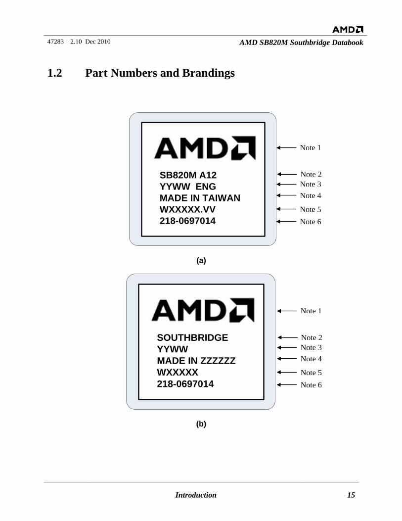
1.2 Part Numbers and Brandings
SB820M A12YYWW ENGMADE IN TAIWANWXXXXX.VV218-0697014
(a)
SOUTHBRIDGEYYWWMADE IN ZZZZZZWXXXXX218-0697014
(b)
Note 2
Note 1
Note 3 Note 4
Note 5 Note 6
Note 2
Note 1
Note 3 Note 4
Note 5 Note 6
47283 2.10 Dec 2010 AMD SB820M Southbridge Databook
Introduction 16
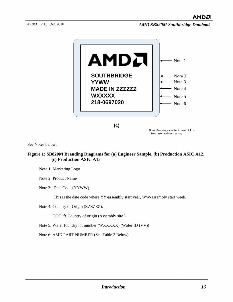
SOUTHBRIDGEYYWWMADE IN ZZZZZZWXXXXX218-0697020
(c)
See Notes below.
Figure 1: SB820M Branding Diagrams for (a) Engineer Sample, (b) Production ASIC A12, (c) Production ASIC A13
Note 1: Marketing Logo
Note 2: Product Name
Note 3: Date Code (YYWW)
This is the date code where YY-assembly start year, WW-assembly start week.
Note 4: Country of Origin (ZZZZZZ).
COO Country of origin (Assembly site )
Note 5: Wafer foundry lot number (WXXXXX) (Wafer ID (VV))
Note 6: AMD PART NUMBER (See Table 2 Below)
Note: Brandings can be in laser, ink, or mixed laser-and-ink marking.
Note 2
Note 1
Note 3 Note 4
Note 5 Note 6
47283 2.10 Dec 2010 AMD SB820M Southbridge Databook
Introduction 17
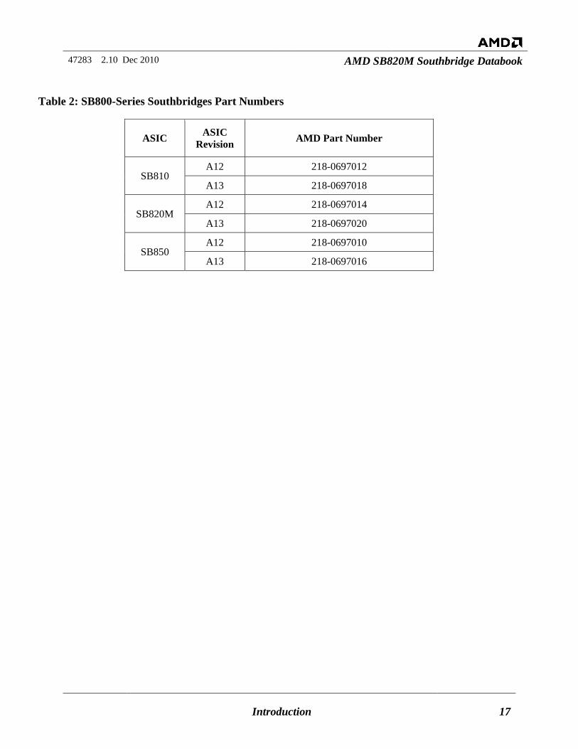
Table 2: SB800-Series Southbridges Part Numbers
ASIC ASIC Revision AMD Part Number
SB810 A12 218-0697012
A13 218-0697018
SB820M A12 218-0697014
A13 218-0697020
SB850 A12 218-0697010
A13 218-0697016
47283 2.10 Dec 2010 AMD SB820M Southbridge Databook
Introduction 18
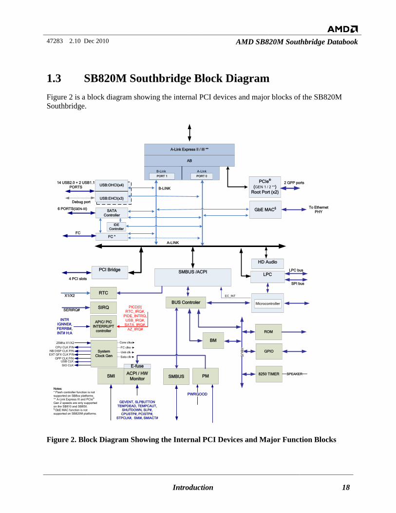
1.3 SB820M Southbridge Block Diagram Figure 2 is a block diagram showing the internal PCI devices and major blocks of the SB820M Southbridge.
SATAController
LPCPCI Bridge SMBUS /ACPI
AB
HD Audio
PORT 1 PORT 0
USB:OHCI(x4)
USB:EHCI(x3)
8250 TIMER
GPIO
BM
RTC
ACPI / HW Monitor SMBUS
ROM
BUS Controler
APIC/ PICINTERRUPT
controller
SMI
SIRQ
PM SPEAKER
GEVENT, SLPBUTTONTEMPDEAD, TEMPCAUT,
SHUTDOWN, SLP#,CPUSTP#, PCISTP#,
STPCLK#, SMI#, SMIACT#
INTRIGNNE#,FERRB#,INT# H:A
PWRGOOD
XB
US
A-LINK
B-LINK
PICD[0]RTC_IRQ#,
PIDE_INTRQ,USB_IRQ#,
SATA_IRQ#,AZ_IRQ#
X1/X2
14 USB2.0 + 2 USB1.1 PORTS
SERIRQ#
4 PCI slots
6 PORTS(GEN-III)
LPC bus
SPI bus
Debug port
B-Link A-Link
FC *FC
A-Link Express II / III **
PCIe® (GEN 1 / 2 **)
Root Port (x2)
2 GPP ports
GbE MAC§
E-fuse
EC_INT
System Clock Gen
25Mhz X1/X2
CPU CLK P/N
EXT GFX CLK P/NGPP CLK P/N
NB DISP CLK P/N
USB CLKSIO CLK
Core clks
FC clks
Usb clk
Sata clk
To Ethernet PHY
Microcontroller
Notes:* Flash controller function is not supported on SB8xx platforms.** A-Link Express III and PCIe® Gen 2 speeds are only supported on the SB810 and SB850.§ GbE MAC function is not supported on SB820M platforms.
IDEController
Figure 2. Block Diagram Showing the Internal PCI Devices and Major Function Blocks
47283 2.10 Dec 2010 AMD SB820M Southbridge Databook
Introduction 19
1.4 Conventions and Notations The following conventions are used throughout this manual.
1.4.1 Pin Names
Pins are identified by their pin names or ball references. All active-low signals are identified by the suffix ‘#’ in their names (e.g., GNT0#).
1.4.2 Pin Types
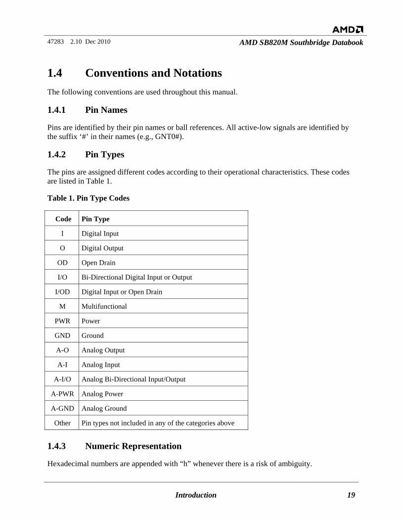
The pins are assigned different codes according to their operational characteristics. These codes are listed in Table 1.
Table 1. Pin Type Codes
Code Pin Type
I Digital Input
O Digital Output
OD Open Drain
I/O Bi-Directional Digital Input or Output
I/OD Digital Input or Open Drain
M Multifunctional
PWR Power
GND Ground
A-O Analog Output
A-I Analog Input
A-I/O Analog Bi-Directional Input/Output
A-PWR Analog Power
A-GND Analog Ground
Other Pin types not included in any of the categories above
1.4.3 Numeric Representation
Hexadecimal numbers are appended with “h” whenever there is a risk of ambiguity.
47283 2.10 Dec 2010 AMD SB820M Southbridge Databook
Introduction 20
Other numbers are in decimal.
Pins of identical functions but different running integers (e.g., “LAD3,” “LAD2,” “LAD3”) are referred to collectively by specifying their integers in square brackets and with colons (i.e., “LAD[3:0]”). A similar short-hand notation is used to indicate bit occupation in a register. For example, Command[15:10] refers to the bit positions 10 through 15 of the Command register.
1.4.4 Register Field
A field of a register is referred to by the format of [Register Name].[Register Field]. For example, “Commad.Memory Space” is the “Memory Space” field of the register “Command.”
1.4.5 Acronyms and Abbreviations
The following is a list of the acronyms and abbreviations used in this manual.
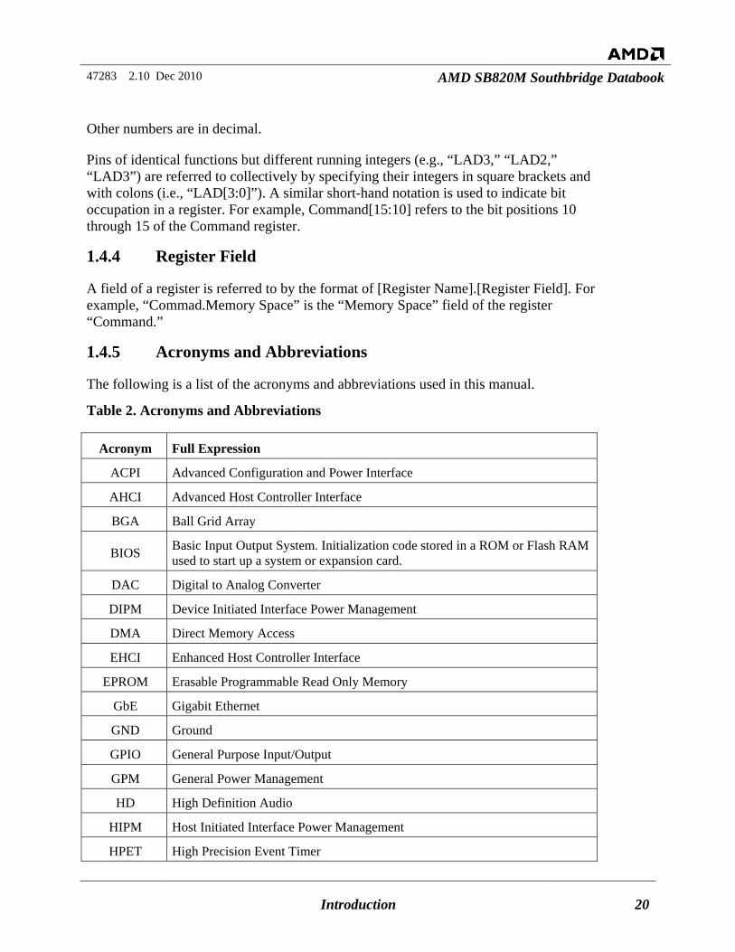
Table 2. Acronyms and Abbreviations
Acronym Full Expression
ACPI Advanced Configuration and Power Interface
AHCI Advanced Host Controller Interface
BGA Ball Grid Array
BIOS Basic Input Output System. Initialization code stored in a ROM or Flash RAM used to start up a system or expansion card.
DAC Digital to Analog Converter
DIPM Device Initiated Interface Power Management
DMA Direct Memory Access
EHCI Enhanced Host Controller Interface
EPROM Erasable Programmable Read Only Memory
GbE Gigabit Ethernet
GND Ground
GPIO General Purpose Input/Output
GPM General Power Management
HD High Definition Audio
HIPM Host Initiated Interface Power Management
HPET High Precision Event Timer
47283 2.10 Dec 2010 AMD SB820M Southbridge Databook
Introduction 21
Acronym Full Expression
I2C Inter-Integrated Circuit
IDE Integrated Drive Electronics
IR Infrared
ISA Industry Standard Architecture
JTAG Joint Test Access Group. An IEEE standard.
LPC Low Pin Count
MAC Medium Access Controller
MII Media Independent Interface
NCQ Native Command Queuing
OHCI Open Host Controller Interface
PCI Peripheral Component Interface
PCIe PCI Express®
PLL Phase Locked Loop
POST Power On Self Test
PD Pull-down Resistor
PU Pull-up Resistor
RAID Redundant Array of Inexpensive Disks
RGMII Reduced Gigabit Media Independent Interface
RTC Real Time Clock
SATA Serial ATA
SB-TSI Sideband Temperature Sensor Interface
SCI System Controller Interrupt
SMBus System Management Bus
SMI System Management Interrupt
SPI Serial Peripheral Interface
TPM Trusted Platform Module
USB Universal Serial Bus
47283 2.10 Dec 2010 AMD SB820M Southbridge Databook
Functional Description 22
Chapter 2 Functional Description
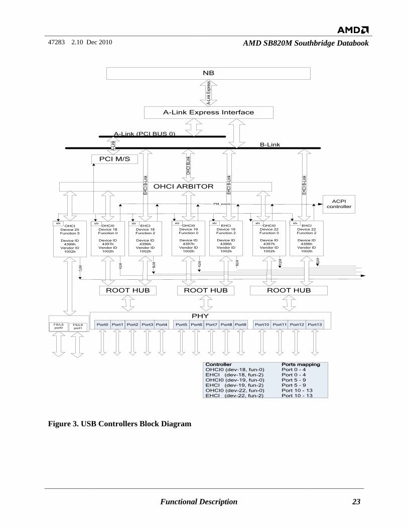
2.1 EHCI USB 2.0 and OHCI USB 1.1 Controllers Figure 3 is an internal block diagram for the SB’s USB controller.
47283 2.10 Dec 2010 AMD SB820M Southbridge Databook
Functional Description 23
ROOT HUB
PHY
OHCI0Device 18 Function 0
Device ID 4397h
Vendor ID 1002h
EHCIDevice 18 Function 2
Device ID 4396h
Vendor ID 1002h
OHCI ARBITOR
A-Li
nkA-Link Express Interface
A-Link (PCI BUS 0)
B-Link
A-Li
nk E
xpre
ss
NB
PCI M/S
slv slv
ACPIcontroller
INTA
EHCI
B-L
ink
INTB
ROOT HUB
INTA
EHCI
B-L
ink
INTB
OHCIDevice 20 Function 5
Device ID 4399h
Vendor ID 1002h
slv
OHC
I BLi
nk
FS/LS port1
Controller Ports mappingOHCI0 (dev-18, fun-0) Port 0 - 4EHCI (dev-18, fun-2) Port 0 - 4OHCI0 (dev-19, fun-0) Port 5 - 9EHCI (dev-19, fun-2) Port 5 - 9OHCI0 (dev-22, fun-0) Port 10 - 13EHCI (dev-22, fun-2) Port 10 - 13
INTCPort0 Port1 Port2 Port3 Port4 Port10 Port11 Port12 Port13
OHCI0Device 19 Function 0
Device ID 4397h
Vendor ID 1002h
EHCIDevice 19Function 2
Device ID 4396h
Vendor ID 1002h
slv slvOHCI0
Device 22 Function 0
Device ID 4397h
Vendor ID 1002h
EHCIDevice 22 Function 2
Device ID 4396h
Vendor ID 1002h
slv slv
EHCI
B-L
ink
INTA
INTB
ROOT HUB
Port5 Port6 Port7 Port8 Port9
PM_event
FS/LS port0
Figure 3. USB Controllers Block Diagram
47283 2.10 Dec 2010 AMD SB820M Southbridge Databook
Functional Description 24
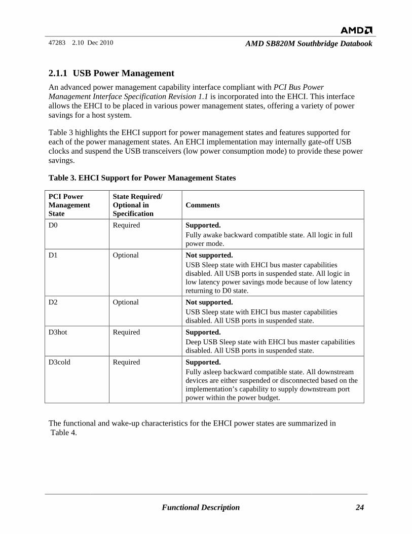
2.1.1 USB Power Management An advanced power management capability interface compliant with PCI Bus Power Management Interface Specification Revision 1.1 is incorporated into the EHCI. This interface allows the EHCI to be placed in various power management states, offering a variety of power savings for a host system.
Table 3 highlights the EHCI support for power management states and features supported for each of the power management states. An EHCI implementation may internally gate-off USB clocks and suspend the USB transceivers (low power consumption mode) to provide these power savings.
Table 3. EHCI Support for Power Management States
PCI Power Management State
State Required/ Optional in Specification
Comments
D0 Required Supported. Fully awake backward compatible state. All logic in full power mode.
D1 Optional Not supported. USB Sleep state with EHCI bus master capabilities disabled. All USB ports in suspended state. All logic in low latency power savings mode because of low latency returning to D0 state.
D2 Optional Not supported. USB Sleep state with EHCI bus master capabilities disabled. All USB ports in suspended state.
D3hot Required Supported. Deep USB Sleep state with EHCI bus master capabilities disabled. All USB ports in suspended state.
D3cold Required Supported. Fully asleep backward compatible state. All downstream devices are either suspended or disconnected based on the implementation’s capability to supply downstream port power within the power budget.
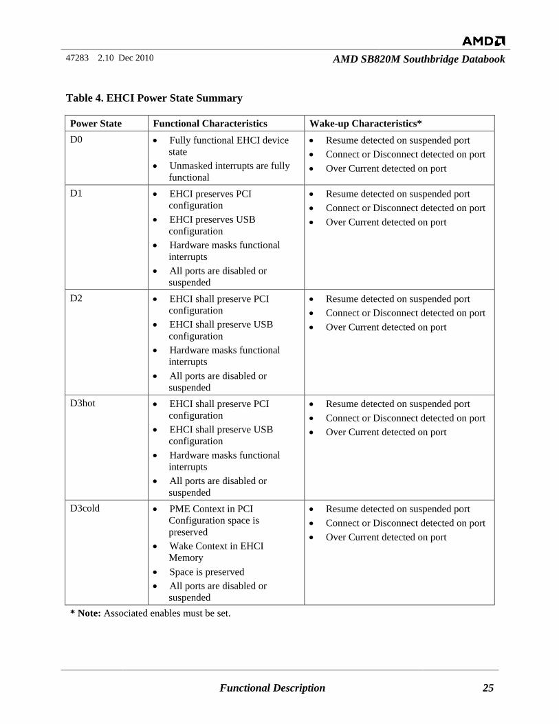
The functional and wake-up characteristics for the EHCI power states are summarized in Table 4.
47283 2.10 Dec 2010 AMD SB820M Southbridge Databook
Functional Description 25
Table 4. EHCI Power State Summary
Power State Functional Characteristics Wake-up Characteristics* D0 • Fully functional EHCI device
state • Unmasked interrupts are fully
functional
• Resume detected on suspended port • Connect or Disconnect detected on port • Over Current detected on port
D1 • EHCI preserves PCI configuration
• EHCI preserves USB configuration
• Hardware masks functional interrupts
• All ports are disabled or suspended
• Resume detected on suspended port • Connect or Disconnect detected on port • Over Current detected on port
D2 • EHCI shall preserve PCI configuration
• EHCI shall preserve USB configuration
• Hardware masks functional interrupts
• All ports are disabled or suspended
• Resume detected on suspended port • Connect or Disconnect detected on port • Over Current detected on port
D3hot • EHCI shall preserve PCI configuration
• EHCI shall preserve USB configuration
• Hardware masks functional interrupts
• All ports are disabled or suspended
• Resume detected on suspended port • Connect or Disconnect detected on port • Over Current detected on port
D3cold • PME Context in PCI Configuration space is preserved
• Wake Context in EHCI Memory
• Space is preserved • All ports are disabled or
suspended
• Resume detected on suspended port • Connect or Disconnect detected on port • Over Current detected on port
* Note: Associated enables must be set.
47283 2.10 Dec 2010 AMD SB820M Southbridge Databook
Functional Description 26
2.2 SMI/SCI Generation Certain system events are routable between SMI or SCI. When an event is routed to SMI, an SMI assertion message will be sent by the SB to the processor and it will enter SMM space. The SMI status remains active until the EOS bit is set. When the EOS is set, an SMI de-assertion message will be sent to the processor. If the event is routed to SCI, BIOS can then route it to any of the legacy interrupts (except IRQ8) or INT21 in the case of IOAPIC.
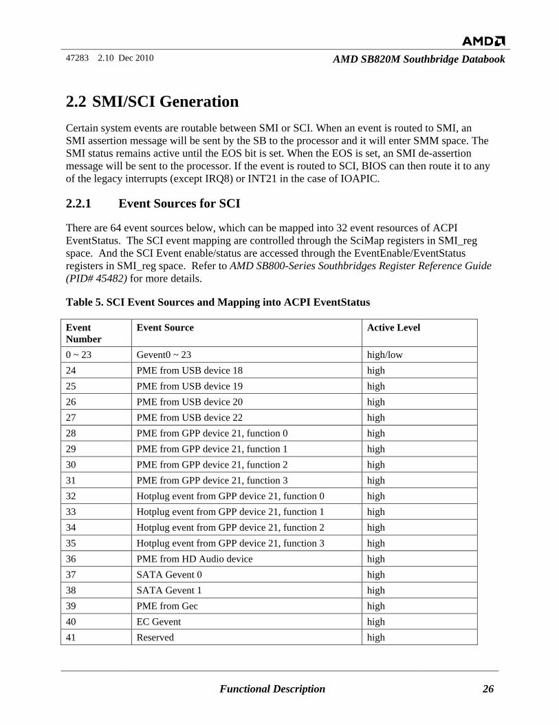
2.2.1 Event Sources for SCI
There are 64 event sources below, which can be mapped into 32 event resources of ACPI EventStatus. The SCI event mapping are controlled through the SciMap registers in SMI_reg space. And the SCI Event enable/status are accessed through the EventEnable/EventStatus registers in SMI_reg space. Refer to AMD SB800-Series Southbridges Register Reference Guide (PID# 45482) for more details.
Table 5. SCI Event Sources and Mapping into ACPI EventStatus
Event Number
Event Source Active Level
0 ~ 23 Gevent0 ~ 23 high/low 24 PME from USB device 18 high 25 PME from USB device 19 high 26 PME from USB device 20 high 27 PME from USB device 22 high 28 PME from GPP device 21, function 0 high 29 PME from GPP device 21, function 1 high 30 PME from GPP device 21, function 2 high 31 PME from GPP device 21, function 3 high 32 Hotplug event from GPP device 21, function 0 high 33 Hotplug event from GPP device 21, function 1 high 34 Hotplug event from GPP device 21, function 2 high 35 Hotplug event from GPP device 21, function 3 high 36 PME from HD Audio device high 37 SATA Gevent 0 high 38 SATA Gevent 1 high 39 PME from Gec high 40 EC Gevent high 41 Reserved high
47283 2.10 Dec 2010 AMD SB820M Southbridge Databook
Functional Description 27
Event Number
Event Source Active Level
42 PME from CIR high 43 Wake# pin high 44 FanThermal Gevent high 45 ASF Master Interrupt event high 46 ASF Slave interrupt event high 47 SMBUS0 interrupt high 48 TWARN event high 49 Traffic Monitor Gevent high 50~ 63 Reserved high
2.2.2 SMI Events
SB820M supports up to 160 sources to generate SMI. The SMI control/status are accessed through the registers defined in the SMI_Reg space. Refer to AMD SB800-Series Southbridges Register Reference Guide (PID# 45482) for more details.
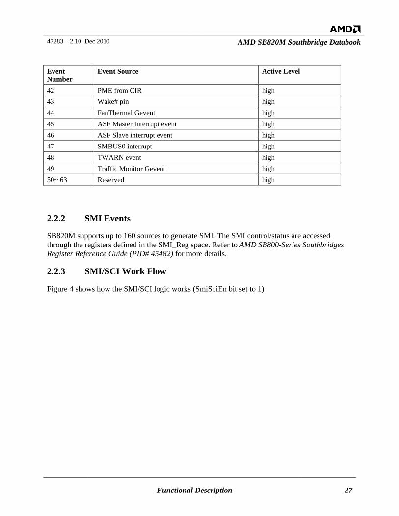
2.2.3 SMI/SCI Work Flow
Figure 4 shows how the SMI/SCI logic works (SmiSciEn bit set to 1)
47283 2.10 Dec 2010 AMD SB820M Southbridge Databook
Functional Description 28
One of the 50 Event Sources
Event Triggered? (SciTrig/edge
triggered)
SmiSciStatus is set
SMI is generated to host (APU)
BIOS SMI service routine acknowledges it by writing 1 to SmiSciStatus to clear
it
ACPI Event trigger logic sees falling edge of
SmiSciStatus
ACPI EventStatus is set and SCI is generated if
EventEnable is set
Yes
No
Figure 4. SMI/SCI Logic of the SB820M
47283 2.10 Dec 2010 AMD SB820M Southbridge Databook
Functional Description 29
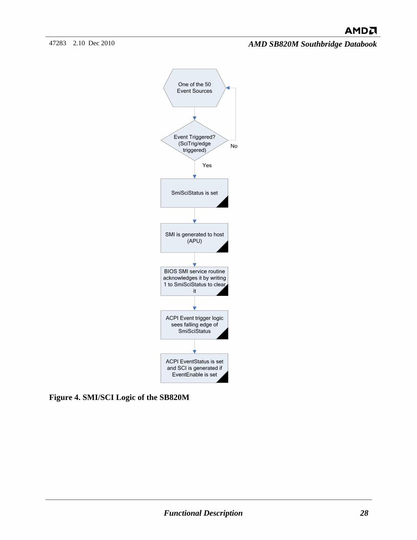
2.3 LPC ISA Bridge 2.3.1 LPC Interface Overview The Low Pin Count (LPC) bus interface is a cost-efficient, low-speed interface designed to support low-speed legacy (ISA, X-bus) devices. The LPC interface essentially eliminates the need of ISA and X-bus in the system. A typical setup of the system with LPC interface is shown in Figure 5. Here the ISA bus is internal to SB and is used for connecting to the legacy Direct Memory Access (DMA) logic. The LPC host controller is typically integrated into the Southbridge. It connects to the internal A-Link bus on one side and the LPC and Serial Peripheral Interface (SPI) buses on the other side.
LPC Device SPI Device
LPC Bridge SPI Bridge
A-Link Bus
Figure 5. SB820M LPC Bus System
Examples of LPC devices include Super I/O (disk controller, keyboard controller), BIOS RAM, audio, Trusted Platform Module (TPM), and system management controller. A BIOS ROM can also be populated on the SPI interface. The SB820M Southbridge can support an LPC or SPI type BIOS ROM. The ROM selection is determined by two strap pins (refer to Table 28. Standard Straps ) during RSMRST# assertion. In addition to the straps, software can change the ROM selection through programming in the PMIO registers.
The ISA interface is only used for legacy DMA operation. LPC host controller has the A-Link bus on one side and the LPC bus on the other. Some LPC signals are used for power management in mobile systems and are optional. A more detailed description of each signal is given later.
The host controller supports memory and I/O read/write, DMA read/write, and bus master memory I/O read/write. It supports up to two bus masters and seven DMA channels. A bus
47283 2.10 Dec 2010 AMD SB820M Southbridge Databook
Functional Description 30
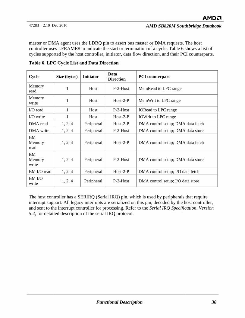
master or DMA agent uses the LDRQ pin to assert bus master or DMA requests. The host controller uses LFRAME# to indicate the start or termination of a cycle. Table 6 shows a list of cycles supported by the host controller, initiator, data flow direction, and their PCI counterparts.
Table 6. LPC Cycle List and Data Direction
Cycle Size (bytes) Initiator Data Direction PCI counterpart
Memory read 1 Host P-2-Host MemRead to LPC range
Memory write 1 Host Host-2-P MemWrit to LPC range
I/O read 1 Host P-2-Host IORead to LPC range I/O write 1 Host Host-2-P IOWrit to LPC range DMA read 1, 2, 4 Peripheral Host-2-P DMA control setup; DMA data fetch DMA write 1, 2, 4 Peripheral P-2-Host DMA control setup; DMA data store BM Memory read
1, 2, 4 Peripheral Host-2-P DMA control setup; DMA data fetch
BM Memory write
1, 2, 4 Peripheral P-2-Host DMA control setup; DMA data store
BM I/O read 1, 2, 4 Peripheral Host-2-P DMA control setup; I/O data fetch BM I/O write 1, 2, 4 Peripheral P-2-Host DMA control setup; I/O data store
The host controller has a SERIRQ (Serial IRQ) pin, which is used by peripherals that require interrupt support. All legacy interrupts are serialized on this pin, decoded by the host controller, and sent to the interrupt controller for processing. Refer to the Serial IRQ Specification, Version 5.4, for detailed description of the serial IRQ protocol.
47283 2.10 Dec 2010 AMD SB820M Southbridge Databook
Functional Description 31
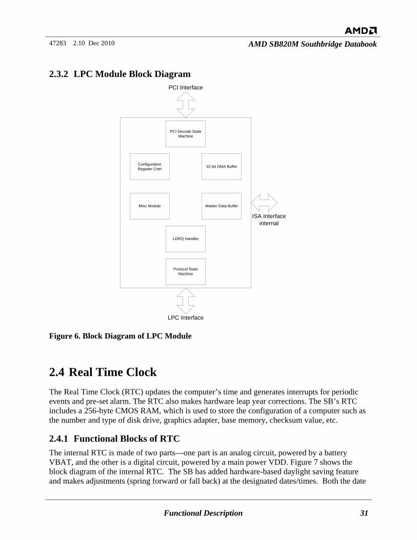
2.3.2 LPC Module Block Diagram
Configuration Register Cntrl 32-bit DMA Buffer
LDRQ Handler
Master Data Buffer
PCI Decode State Machine
Protocol State Machine
Misc Module
PCI Interface
LPC Interface
ISA Interface internal
Figure 6. Block Diagram of LPC Module
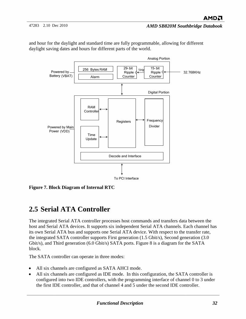
2.4 Real Time Clock The Real Time Clock (RTC) updates the computer’s time and generates interrupts for periodic events and pre-set alarm. The RTC also makes hardware leap year corrections. The SB’s RTC includes a 256-byte CMOS RAM, which is used to store the configuration of a computer such as the number and type of disk drive, graphics adapter, base memory, checksum value, etc.
2.4.1 Functional Blocks of RTC The internal RTC is made of two parts—one part is an analog circuit, powered by a battery VBAT, and the other is a digital circuit, powered by a main power VDD. Figure 7 shows the block diagram of the internal RTC. The SB has added hardware-based daylight saving feature and makes adjustments (spring forward or fall back) at the designated dates/times. Both the date
47283 2.10 Dec 2010 AMD SB820M Southbridge Databook
Functional Description 32
and hour for the daylight and standard time are fully programmable, allowing for different daylight saving dates and hours for different parts of the world.
256 Bytes RAM 29- bit Ripple
Counter
15- bit Ripple
Counter
1Hz32.768KHz
Analog Portion
Decode and Interface
Registers Frequency
Divider
Alarm
RAM Controller
Time Update
Digital Portion
To PCI Interface
Powered by Battery (VBAT)
Powered by Main Power (VDD)
Figure 7. Block Diagram of Internal RTC
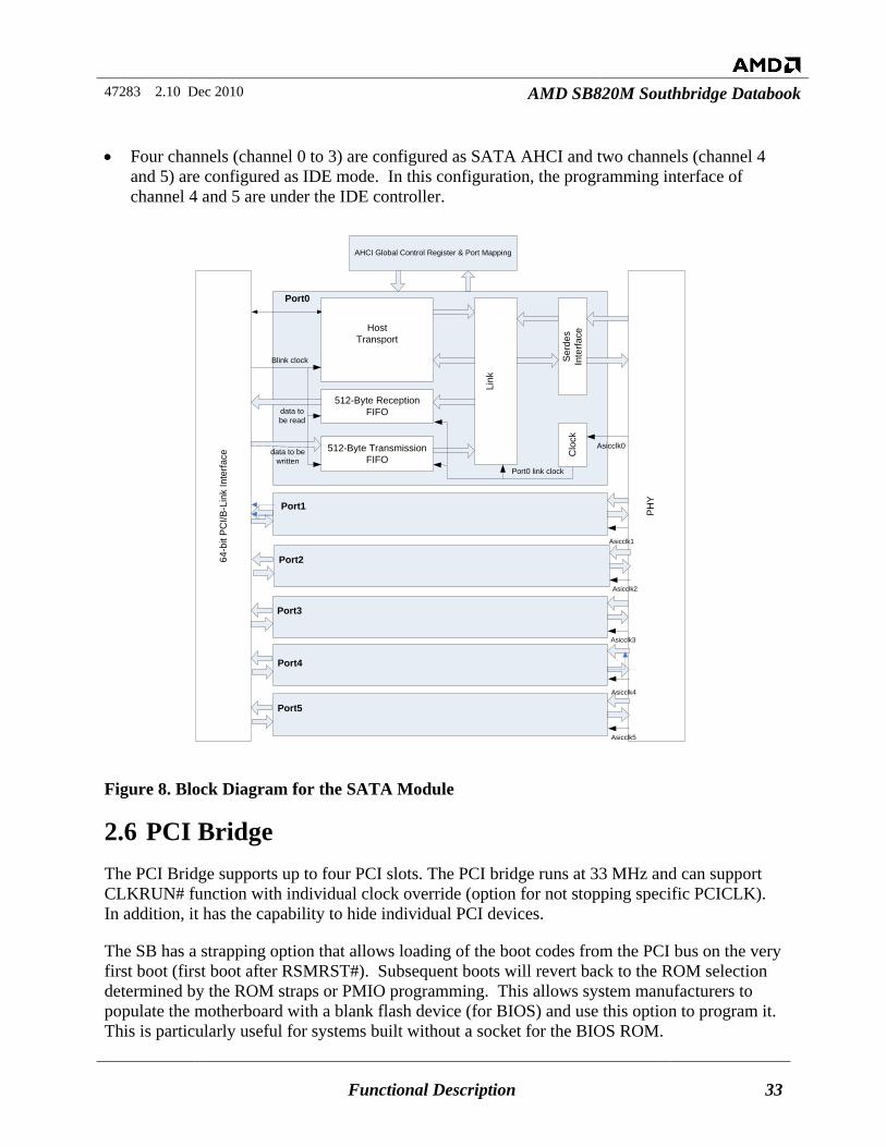
2.5 Serial ATA Controller The integrated Serial ATA controller processes host commands and transfers data between the host and Serial ATA devices. It supports six independent Serial ATA channels. Each channel has its own Serial ATA bus and supports one Serial ATA device. With respect to the transfer rate, the integrated SATA controller supports First generation (1.5 Gbit/s), Second generation (3.0 Gbit/s), and Third generation (6.0 Gbit/s) SATA ports. Figure 8 is a diagram for the SATA block.
The SATA controller can operate in three modes:
• All six channels are configured as SATA AHCI mode. • All six channels are configured as IDE mode. In this configuration, the SATA controller is
configured into two IDE controllers, with the programming interface of channel 0 to 3 under the first IDE controller, and that of channel 4 and 5 under the second IDE controller.
47283 2.10 Dec 2010 AMD SB820M Southbridge Databook
Functional Description 33
• Four channels (channel 0 to 3) are configured as SATA AHCI and two channels (channel 4 and 5) are configured as IDE mode. In this configuration, the programming interface of channel 4 and 5 are under the IDE controller.
512-Byte Reception FIFO
512-Byte Transmission FIFO
64-b
it PC
I/B-L
ink
Inte
rface
data to be read
data to be written
Serd
esIn
terfa
ce
PHY
Link
HostTransport
Clo
ck
Asicclk0
Port0 link clock
Blink clock
Port0
Port3
Port1
AHCI Global Control Register & Port Mapping
Asicclk3
Asicclk1
Port2
Asicclk2
Port4
Asicclk4
Port5
Asicclk5
Figure 8. Block Diagram for the SATA Module
2.6 PCI Bridge The PCI Bridge supports up to four PCI slots. The PCI bridge runs at 33 MHz and can support CLKRUN# function with individual clock override (option for not stopping specific PCICLK). In addition, it has the capability to hide individual PCI devices.
The SB has a strapping option that allows loading of the boot codes from the PCI bus on the very first boot (first boot after RSMRST#). Subsequent boots will revert back to the ROM selection determined by the ROM straps or PMIO programming. This allows system manufacturers to populate the motherboard with a blank flash device (for BIOS) and use this option to program it. This is particularly useful for systems built without a socket for the BIOS ROM.
47283 2.10 Dec 2010 AMD SB820M Southbridge Databook
Functional Description 34
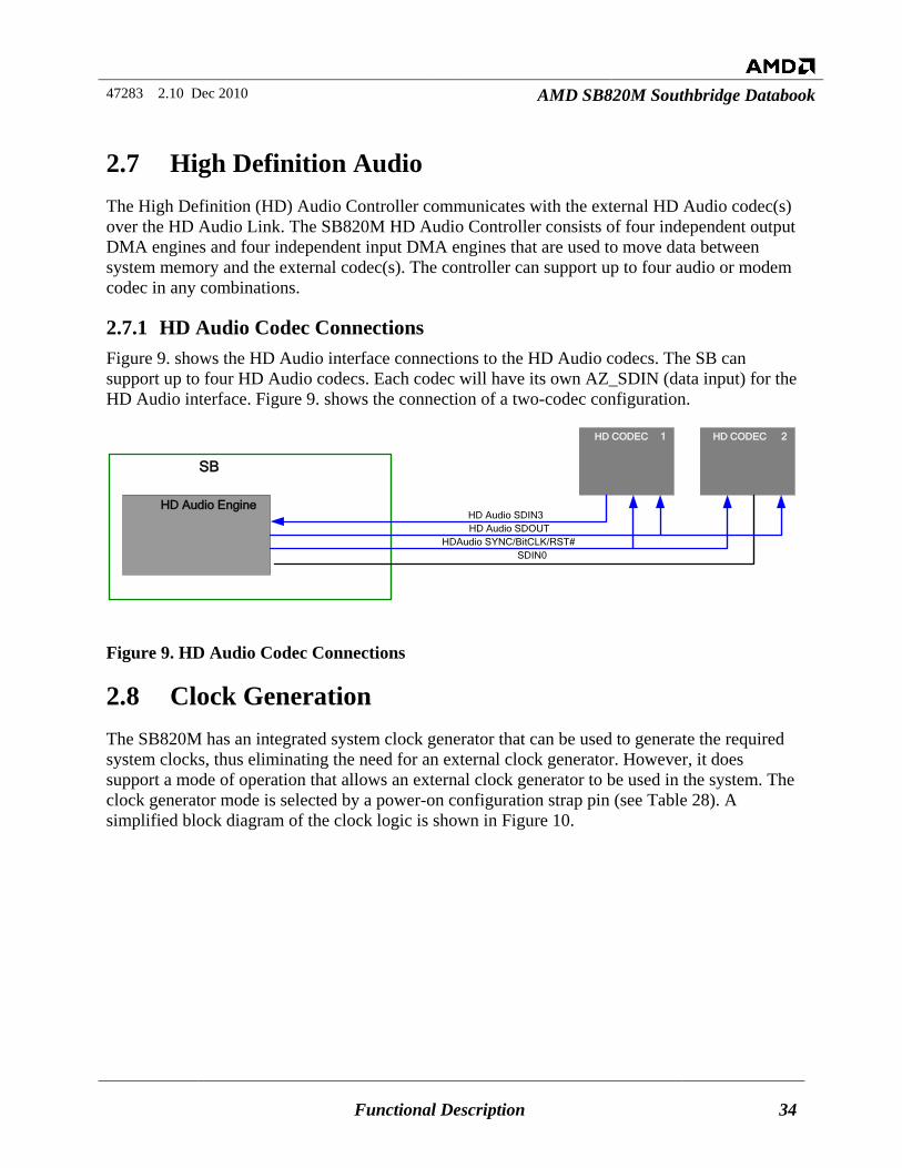
2.7 High Definition Audio The High Definition (HD) Audio Controller communicates with the external HD Audio codec(s) over the HD Audio Link. The SB820M HD Audio Controller consists of four independent output DMA engines and four independent input DMA engines that are used to move data between system memory and the external codec(s). The controller can support up to four audio or modem codec in any combinations.
2.7.1 HD Audio Codec Connections Figure 9. shows the HD Audio interface connections to the HD Audio codecs. The SB can support up to four HD Audio codecs. Each codec will have its own AZ_SDIN (data input) for the HD Audio interface. Figure 9. shows the connection of a two-codec configuration.
SB
HD Audio Engine
HD CODEC 1 HD CODEC 2
SDIN0HDAudio SYNC/BitCLK/RST#
HD Audio SDOUTHD Audio SDIN3
Figure 9. HD Audio Codec Connections
2.8 Clock Generation The SB820M has an integrated system clock generator that can be used to generate the required system clocks, thus eliminating the need for an external clock generator. However, it does support a mode of operation that allows an external clock generator to be used in the system. The clock generator mode is selected by a power-on configuration strap pin (see Table 28). A simplified block diagram of the clock logic is shown in Figure 10.
47283 2.10 Dec 2010 AMD SB820M Southbridge Databook
Functional Description 35
GPP 2
GPP 10
GPP 1
PCIe_GPP1(diff)
PCIe_GPP2(diff)
Gfx
SIO 48/25/14Mhz
SB8xx
25Mhz XTAL
SB8xx System Level Clocks Distribution Diagram
PC
Ie_N
B(d
iff)
100M
Hz NB
_DS
PLL
_CLK
100M
Hz
NB
_HT
_CLK
(diff
)10
0MH
z
CPU_HT_CLK(diff)200MHz
Device_CLK (48/25/14MHz)
Any device on system or
NB
SLT
_GF
X_C
LK(d
iff)
100M
Hz
GPP 9PCIe_GPP9(diff)
System clock gen
14Mhz
CPU
NB
Pci Clk (x7)
Figure 10. System Clock Generation
If the SB820M is in external clock mode, the clock sources it requires are a 25MHz crystal as internal PLL clock source, a 32-KHz crystal for the RTC, and a 100MHz differential clock pair for the PCIe reference clocks. In addition to the PCIe clocks, the SB820M also uses the 100 MHz clock to generate various internal clocks, including the PCI 33-MHz clocks.
If the SB820M is set to integrated clock mode, only a 25MHz crystal for master reference and a 32-KHz crystal for the RTC are required. The SB820M will then generate all of the system clocks needed, which include the CPU, NB, and graphics reference clocks, the 25MHz clock for SATA, the 48MHz clocks for USB, and so on. Overclocking is not supported in the internal clock mode.
The requirements for clock sources for both the internal and external modes are detailed in Table 53, “System Clock Input Source Descriptions.”
47283 2.10 Dec 2010 AMD SB820M Southbridge Databook
Functional Description 36
2.9 Power Management/ACPI The SB820M power management/ACPI logic is identical to that of the SB700. It supports C3/C1e and stutter mode and S states.
47283 2.10 Dec 2010 AMD SB820M Southbridge Databook
Ballout Assignment 37
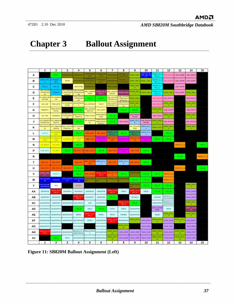
Chapter 3 Ballout Assignment
1 2 3 4 5 6 7 8 9 10 11 12 13 14 15
A xxxxxxxxxxxxxxx VSS_3 VIN0/GPIO175 VIN2/GPIO177 TEMPIN2/GPIO173
TEMPIN1/GPIO172 VIN4/GPIO179 VIN7/GBE_LE
D3/GPIO182 VSSIO_USB_1USBCLK/14M_25M_48M_OS
C
VDDCR_11_USB_S_1 USB_HSD13N USB_HSD9P USB_HSD4N
B VDDBT_RTC_G
INTRUDER_ALERT# TEST0 VIN1/GPIO176
TEMPIN3/TALERT#/GPIO17
4
TEMPIN0/GPIO171 VIN5/GPIO180 VIN6/GBE_ST
AT3/GPIO181 VSSIO_USB_4 VSSIO_USB_2 VDDCR_11_USB_S_2 USB_HSD13P USB_HSD9N USB_HSD4P
C 32K_X1 32K_X2 TEST1/TMS VIN3/GPIO178 TEMP_COMM VSSIO_USB_14
VDDAN_11_USB_S_1 USB_HSD8N
DUSB_OC6#/IR_TX1/GEVENT
6#RTCCLK
SPI_CS3#/GBE_STAT1/GEV
ENT21#
USB_OC4#/IR_RX0/GEVENT
16#
GBE_LED0/GPIO183
VDDAN_33_HWM_S
GBE_LED1/GEVENT9# VSSAN_HWM VSSIO_USB_1
7 VSSIO_USB_5 VDDAN_11_USB_S_2 VSSIO_USB_6 USB_HSD8P VSSIO_USB_7
E IR_LED#/LLB#/GPIO184
SPI_DO/GPIO163
USB_OC5#/IR_TX0/GEVENT
17#VSS_4 VSS_7 USB_OC1#/TD
I/GEVENT13#
USB_OC3#/AC_PRES/TDO/G
EVENT15#VSSIO_USB_9 USB_HSD12N USB_HSD11N USB_HSD11P
F SLP_S3# PWR_BTN# IR_RX1/GEVENT20#
SDA1/GPIO228 SCL1/GPIO227 TEST2 USB_OC2#/TC
K/GEVENT14#
USB_OC0#/TRST#/GEVENT1
2#
VSSIO_USB_10 USB_HSD12P VSSIO_USB_1
1VSSIO_USB_1
2
G RSMRST# ROM_RST#/GPIO161 VSS_40 GBE_LED2/GE
VENT10# SUS_STAT# VSS_42 VSS_43 VSSIO_USB_15 USB_HSD7P USB_HSD7N
H SLP_S5# GEVENT5#BLINK/USB_OC7#/GEVENT1
8#
DDR3_RST#/GEVENT7# PWR_GOOD WAKE#/GEVE
NT8# VSS_46 USB_FSD0P/GPIO185 USB_FSD1N VSSIO_USB_1
8VSSIO_USB_1
9
J SYS_RESET#/GEVENT19#
PCI_PME#/GEVENT4# VSS_41 SPI_DI/GPIO1
64
THRMTRIP#/SMBALERT#/G
EVENT2#VSS_21 USB_FSD0N VDDIO_33_S_
6USB_FSD1P/G
PIO186VSSIO_USB_2
2 USB_HSD10P USB_HSD10N
K RI#/GEVENT22#
LPC_PME#/GEVENT3#
GBE_STAT0/GEVENT11#
SPI_CLK/GPIO162
SPI_CS1#/GPIO165
VDDIO_33_S_4 VSSIO_USB_3 VSSIO_USB_2
4VSSIO_USB_2
5
L A_RST# AZ_SDIN0/GPIO167 VSS_51 GBE_MDIO GBE_MDCK VDDCR_11_G
BE_S_1 VSS_52 VDDCR_11_GBE_S_2
VDDIO_33_S_5 VSS_19
M AZ_SDIN2/GPIO169
AZ_SDIN1/GPIO168 AZ_BITCLK AZ_SDIN3/GPI
O170 GBE_TXD3 VDDIO_GBE_S_1
GBE_TXCTL/TXEN VDDIO_AZ_S GBE_PHY_RS
T#VDDIO_33_GB
E_S VSS_18 VSS_44
N AZ_SDOUT AZ_SYNC VSS_50 VDDCR_11_1 VSS_9
P PCIE_RST# AZ_RST# VSS_22 GBE_PHY_PD GBE_TXCLK VSS_49 GBE_TXD0 VDDIO_GBE_S_2 GBE_TXD2 VSS_13
R VSS_10 VDDCR_11_2
T GBE_COL GBE_RXD1 GBE_CRS GBE_RXCTL/RXDV
VDDIO_33_S_7 GBE_TXD1 VDDIO_33_S_
8 GBE_RXCLK VSS_12
U GBE_RXD3 GBE_RXD0 GBE_RXD2 VSS_33 VDDCR_11_4 VSS_15
V VDDRF_GBE_S PCIRST# VSS_23 GBE_RXERR VDDIO_33_PC
IGP_2GBE_PHY_INT
R VSS_28 FANIN1/GPIO57 VSS_48 VSS_14 VDDCR_11_6
W PCICLK1/GPO36 PCICLK0 PCICLK2/GPO
37PCICLK3/GPO
38FANOUT0/GPIO52
FANOUT1/GPIO53
FANIN0/GPIO56
FANIN2/GPIO58 VSS_29 VSS_30 VDDCR_11_8
Y PCICLK4/14M_OSC/GPO39 NC2 EFUSE FANOUT2/GPI
O54 VSS_35 VSS_37 VSS_36 VSSIO_SATA_1
AA AD0/GPIO0 VDDIO_33_PCIGP_6 AD2/GPIO2 AD1/GPIO1 AD4/GPIO4 AD8/GPIO8 VDDIO_33_PC
IGP_9 CBE0# VDDIO_33_PCIGP_10 CBE3# VSS_38 VSS_39 SATA_CALRN
AB AD3/GPIO3 AD5/GPIO5 VDDIO_33_PCIGP_7 AD7/GPIO7 AD6/GPIO6 VSS_26 DEVSEL# CLKRUN# GNT3#/CLK_R
EQ7#/GPIO46 SATA_CALRP
AC AD12/GPIO12 AD9/GPIO9 AD10/GPIO10 AD11/GPIO11 PAR AD15/GPIO15 VDDIO_33_PCIGP_8 VSS_27 AD25/GPIO25 REQ3#/CLK_R
EQ5#/GPIO42VSSIO_SATA_
4
AD AD13/GPIO13 AD14/GPIO14 VSS_25 CBE1# VSS_24 LOCK# CBE2# AD24/GPIO24 SATA_ACT#/GPIO67 GNT0# VDDPL_33_SA
TA
AE AD17/GPIO17 AD16/GPIO16 AD19/GPIO19 SERR# VDDIO_33_PCIGP_4 PERR# TRDY# FRAME# AD23/GPIO23 REQ0# VSSIO_SATA_
5VSSIO_SATA_
6
AF AD20/GPIO20 AD22/GPIO22 AD28/GPIO28 AD27/GPIO27 STOP# AD26/GPIO26 VDDIO_33_PCIGP_11 AD18/GPIO18 VSSIO_SATA_
7 SATA_RX1P VSSIO_SATA_8 SATA_TX2N VSSIO_SATA_
9 SATA_RX3P
AG AD21/GPIO21 AD30/GPIO30 INTG#/GPIO34 INTF#/GPIO33 VSSIO_SATA_11 SATA_RX1N SATA_TX2P SATA_RX3N
AH VDDIO_33_PCIGP_1 AD29/GPIO29 AD31/GPIO31 REQ2#/CLK_R
EQ8#/GPIO41REQ1#/GPIO4
0 GNT2#/GPO45 VSSIO_SATA_12 SATA_RX0P SATA_TX0P SATA_TX1P VSSIO_SATA_
13 SATA_RX2P VSSIO_SATA_14 SATA_TX3P
AJ VSS_1 IRDY# INTH#/GPIO35 GNT1#/GPO44 INTE#/GPIO32 VSSIO_SATA_16 SATA_RX0N SATA_TX0N SATA_TX1N VSSIO_SATA_
17 SATA_RX2N VSSIO_SATA_18 SATA_TX3N
1 2 3 4 5 6 7 8 9 10 11 12 13 14 15
Figure 11: SB820M Ballout Assignment (Left)
47283 2.10 Dec 2010 AMD SB820M Southbridge Databook
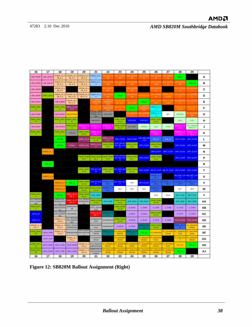
Ballout Assignment 38
16 17 18 19 20 21 22 23 24 25 26 27 28 29USB_HSD0P USB_HSD1N VDDAN_33_U
SB_S_1VDDAN_33_U
SB_S_2VDDAN_33_U
SB_S_3VDDIO_33_S_
1KSO_16/GPIO
225KSO_13/GPIO
222KSO_6/GPIO2
15KSO_8/GPIO2
17KSO_4/GPIO2
13KSO_1/GPIO2
10 VSS_2 A
USB_HSD0N USB_HSD1P VDDAN_33_USB_S_4
VDDAN_33_USB_S_5
VDDAN_33_USB_S_6
VDDIO_33_S_3
KSO_17/GPIO226
KSO_12/GPIO221
KSO_10/GPIO219
KSO_7/GPIO216
SCL3_LV/GPIO195
KSO_2/GPIO211
KSO_0/GPIO209 VSS_32 B
USB_HSD5N VDDAN_33_USB_S_7
VDDAN_33_USB_S_8
KSO_15/GPIO224
KSO_11/GPIO220
KSO_5/GPIO214
KSI_7/GPIO208
KSI_6/GPIO207 C
USB_HSD5P VSSIO_USB_8 VDDAN_33_USB_S_9
VDDAN_33_USB_S_10
VDDAN_33_USB_S_11
VDDIO_33_S_2
KSO_14/GPIO223 VSS_5 KSO_9/GPIO2
18 SCL2/GPIO193 KSO_3/GPIO212
PS2KB_DAT/GPIO189
KSI_5/GPIO206
KSI_4/GPIO205 D
USB_HSD3N USB_HSD3P VDDAN_33_USB_S_12
EC_PWM3/EC_TIMER3/GPI
O200
EC_PWM1/EC_TIMER1/GPI
O198
PS2_DAT/SDA4/GPIO187
PS2_CLK/SCL4/GPIO188 VSS_6 SDA3_LV/GPI
O196PS2M_CLK/GP
IO192KSI_2/GPIO20
3KSI_3/GPIO20
4 EVSSIO_USB_1
3VSSIO_USB_1
6VDDPL_33_US
B_S
SPI_CS2#/GBE_STAT2/GPI
O166
EC_PWM2/EC_TIMER2/GPI
O199
SDA2/GPIO194 VSS_8
EC_PWM0/EC_TIMER0/GPI
O197
VDDCR_11_S_1
PS2KB_CLK/GPIO190
PS2M_DAT/GPIO191 F
USB_HSD6P USB_HSD6N USB_RCOMPALLOW_LDTSTP/DMA_ACTI
VE#LDT_STP# KSI_0/GPIO20
1KSI_1/GPIO20
2VDDCR_11_S
_2 NC1 LFRAME# FC_RST#/GPO160 G
VSSIO_USB_20
VSSIO_USB_21
VSSIO_USB_28 PROCHOT# VSSIO_PCIEC
LK_14 LPCCLK0 LPCCLK1 VSSIO_PCIECLK_15 LAD3 LAD2 H
USB_HSD2P USB_HSD2N VSSIO_USB_23
VDDAN_11_CLK_6
VDDAN_11_CLK_5
VDDAN_11_CLK_8
VSSIO_PCIECLK_13 LDT_RST# LDRQ0# LAD1 LAD0 VDDAN_11_C
LK_3LPC_SMI#/GE
VENT23# JVSSIO_USB_2
6VSSIO_USB_2
7 LDT_PG VSSIO_PCIECLK_27
VDDAN_11_CLK_7
VDDAN_11_CLK_4
VDDAN_11_CLK_1
VDDAN_11_CLK_2 K
VSS_20 VDDXL_33_S VSSIO_PCIECLK_26
VDDPL_11_SYS_S GPP_CLK4N GPP_CLK4P 14M_25M_48M
_OSC 25M_X1 25M_X2 GPP_CLK0N GPP_CLK0P L
VSS_16 VSSXL VSSPL_SYS VDDPL_33_SYS
VSSIO_PCIECLK_3
PCIE_RCLKP/NB_LNK_CLK
P
VSSIO_PCIECLK_4 GPP_CLK5N VSSIO_PCIEC
LK_5 GPP_CLK2N GPP_CLK2P M
VDDCR_11_3 GPP_CLK7P GPP_CLK7N GPP_CLK1N GPP_CLK1P NVSSIO_PCIEC
LK_2VSSIO_PCIEC
LK_1VSSIO_PCIEC
LK_6
PCIE_RCLKN/NB_LNK_CLK
N
VSSIO_PCIECLK_7 GPP_CLK5P VSSIO_PCIEC
LK_8 GPP_CLK6N GPP_CLK6P P
VSS_11 RVSSIO_PCIEC
LK_9CPU_HT_CLK
NVSSIO_PCIEC
LK_10SLT_GFX_CLK
NVSSIO_PCIEC
LK_11 GPP_CLK3P NB_HT_CLKP NB_HT_CLKN GPP_CLK8N GPP_CLK8P T
VDDCR_11_5 VDDAN_11_PCIE_1
NB_DISP_CLKN
NB_DISP_CLKP U
VDDCR_11_7 VSS_17 VSSIO_PCIECLK_12
CPU_HT_CLKP
VDDAN_11_PCIE_2
SLT_GFX_CLKP NC3 GPP_CLK3N VDDAN_11_P
CIE_3VDDAN_11_P
CIE_4VDDAN_11_P
CIE_5VDDAN_11_P
CIE_6 V
VDDCR_11_9 VSSIO_PCIECLK_24
VSSIO_PCIECLK_23
VDDAN_11_PCIE_7 NC4 NC5 NC6 VDDAN_11_P
CIE_8 NC7 NC8 WVSSIO_SATA_
2 VSS_34 VDDIO_33_PCIGP_3
VSSIO_PCIECLK_22 GPP_RX0N NC9 NC10 GPP_TX1N GPP_TX1P Y
CLK_REQ3#/SATA_IS1#/GPI
O63
LDRQ1#/CLK_REQ6#/GPIO4
9
VDDIO_33_PCIGP_12
CLK_REQG#/GPIO65/OSCI
N
VSSIO_PCIECLK_16 GPP_RX0P VSSIO_PCIEC
LK_17 GPP_RX1N GPP_RX1P VSSIO_PCIECLK_20 GPP_TX0P GPP_TX0N AA
VSSIO_SATA_3
CLK_REQ1#/FANOUT4/GPIO
61
SERIRQ/GPIO48
SMARTVOLT1/SATA_IS2#/GP
IO50
VSSIO_PCIECLK_18 A_RX3N A_RX3P A_TX3P A_TX3N A_TX2N A_TX2P AB
SATA_X2CLK_REQ0#/SATA_IS3#/GPI
O60NB_PWRGD VDDIO_33_PC
IGP_5VDDIO_18_FC
_4 A_RX2P A_RX2N VSSIO_PCIECLK_21 A_TX1P A_TX1N AC
SATA_X1 VDDAN_11_SATA_6
CLK_REQ4#/SATA_IS0#/GPI
O64
GA20IN/GEVENT0# SCL0/GPIO43 VSSIO_PCIEC
LK_19 A_RX1N A_RX1P A_TX0P A_TX0N PCIE_CALRN PCIE_CALRP ADVDDAN_11_S
ATA_7VDDAN_11_S
ATA_5SATA_IS5#/FANIN3/GPIO59
KBRST#/GEVENT1# SDA0/GPIO47 A_RX0N A_RX0P VDDIO_18_FC
_2VSSIO_PCIEC
LK_25VDDPL_33_PC
IEFC_CE2#/GPI
OD150 AEVSSIO_SATA_
10 SATA_TX4N VDDAN_11_SATA_4 SPKR/GPIO66
SATA_IS4#/FANOUT3/GPIO5
5
FC_ADQ8/GPIOD136
VDDIO_18_FC_1
FC_ADQ11/GPIOD139
VDDIO_18_FC_3 VSS_45 FC_FBCLKIN FC_CE1#/GPI
OD149FC_OE#/GPIO
D145FC_INT1/GPIO
D144 AF
SATA_TX4P VDDAN_11_SATA_3
FC_ADQ7/GPIOD135
FC_ADQ4/GPIOD132
FC_ADQ14/GPIOD142
FC_WE#/GPIOD148
FC_FBCLKOUT
FC_AVD#/GPIOD146 AG
VSSIO_SATA_15 SATA_RX4P SATA_TX5N SATA_RX5N VDDAN_11_S
ATA_2CLK_REQ2#/FANIN4/GPIO62
FC_ADQ9/GPIOD137
FC_ADQ5/GPIOD133
FC_ADQ3/GPIOD131
FC_ADQ2/GPIOD130
FC_ADQ15/GPIOD143
FC_INT2/GPIOD147 FC_CLK VSS_47 AH
VSSIO_SATA_19 SATA_RX4N SATA_TX5P SATA_RX5P VDDAN_11_S
ATA_1
SMARTVOLT2/SHUTDOWN#/
GPIO51
FC_ADQ6/GPIOD134
FC_ADQ10/GPIOD138
FC_ADQ12/GPIOD140
FC_ADQ13/GPIOD141
FC_ADQ1/GPIOD129
FC_ADQ0/GPIOD128 VSS_31 AJ
16 17 18 19 20 21 22 23 24 25 26 27 28 29
Figure 12: SB820M Ballout Assignment (Right)
47283 2.10 Dec 2010 AMD SB820M Southbridge Databook
Pin Descriptions 39
Chapter 4 Pin Descriptions
Note: For multi-functional pins, go to the relevant section for description of a specific function (e.g., for USB_FSD1P/GPIO186, the USB_FSD1P function is described in Section 4.6, ”USB Interface,” and the GPIO186 function is described in Section 4.15, “General Purpose I/O”).
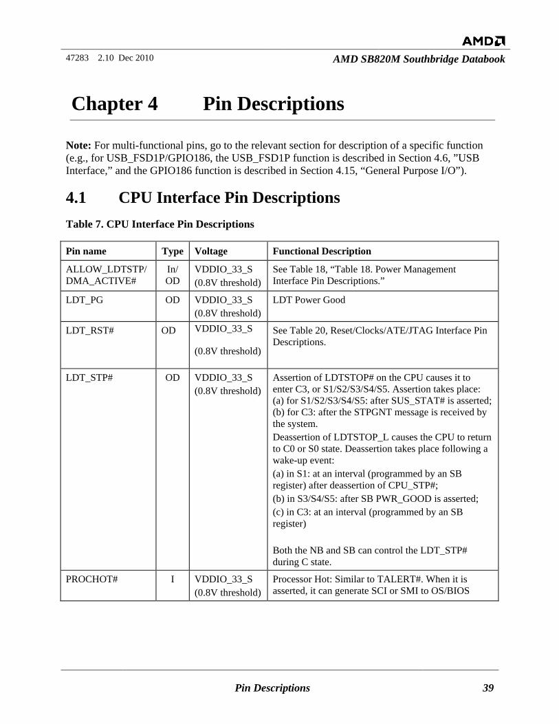
4.1 CPU Interface Pin Descriptions Table 7. CPU Interface Pin Descriptions
Pin name Type Voltage Functional Description
ALLOW_LDTSTP/DMA_ACTIVE#
In/ OD
VDDIO_33_S (0.8V threshold)
See Table 18, “Table 18. Power Management Interface Pin Descriptions.”
LDT_PG OD VDDIO_33_S (0.8V threshold)
LDT Power Good
LDT_RST# OD VDDIO_33_S
(0.8V threshold)
See Table 20, Reset/Clocks/ATE/JTAG Interface Pin Descriptions.
LDT_STP# OD VDDIO_33_S (0.8V threshold)
Assertion of LDTSTOP# on the CPU causes it to enter C3, or S1/S2/S3/S4/S5. Assertion takes place: (a) for S1/S2/S3/S4/S5: after SUS_STAT# is asserted; (b) for C3: after the STPGNT message is received by the system. Deassertion of LDTSTOP_L causes the CPU to return to C0 or S0 state. Deassertion takes place following a wake-up event: (a) in S1: at an interval (programmed by an SB register) after deassertion of CPU_STP#; (b) in S3/S4/S5: after SB PWR_GOOD is asserted; (c) in C3: at an interval (programmed by an SB register) Both the NB and SB can control the LDT_STP# during C state.
PROCHOT# I VDDIO_33_S (0.8V threshold)
Processor Hot: Similar to TALERT#. When it is asserted, it can generate SCI or SMI to OS/BIOS
47283 2.10 Dec 2010 AMD SB820M Southbridge Databook
Pin Descriptions 40
4.2 LPC Interface Pin Descriptions Table 8. LPC Interface Pin Descriptions
Pin Name Type Voltage Functional Description
GA20IN/GEVENT0# I 3.3V (5-V tolerance)
A20 Gate Input from SIO / General Event 0
KBRST#/ GEVENT1#
I 3.3V (5-V tolerance)
Keyboard reset# / General Event 1
LAD[3:0] I/O VDDIO_33_S Multiplexed Command / Address/Data [3:0]
LDRQ0# I VDDIO_33_S Encoded DMA Bus Master Request 0
LDRQ1#/ CLK_REQ6#/ GPIO49
I/O 3.3V (5-V tolerance)
Encoded DMA Bus Master Request 1 / Clock Request 6 / GPIO 49
LFRAME# O VDDIO_33_S LPC Bus Frame. Indicates start of a new cycle or termination of a broken cycle.
LPCCLK0 O VDDIO_33_S 33MHz LPCCLK for LPC device such as flash ROM
LPCCLK1 O VDDIO_33_S 33MHz LPCCLK for LPC device such as SIO device
LPC_SMI#/ GEVNT23#
I VDDIO_33_S LPC SMI / General Event 23
SERIRQ/GPIO48 I/O 3.3V (5-V tolerance)
Serial IRQ / GPIO 48
Note: LPCCLK0 can be assigned to any LPC device. This clock is active during S2 – S5 states. LPCCLK1 and PCI Clock can be used for additional LPC devices that do not require clock in S2 –S5 states.
4.3 A-Link Express II Interface Pin Descriptions Table 9. A-Link Express II Interface Pin Descriptions
Pin Name Type Voltage Functional Description
A_TX[3:0]P O
1.1V (Filtered)
A-Link Express II Lane 3-0 Transmit Positive
A_TX[3:0]N O A-Link Express II Lane 3-0 Transmit Negative
A_RX[3:0]P I A-Link Express II Lane 3-0 Receive Positive
A_RX[3:0]N I A-Link Express II Lane 3-0 Receive Negative
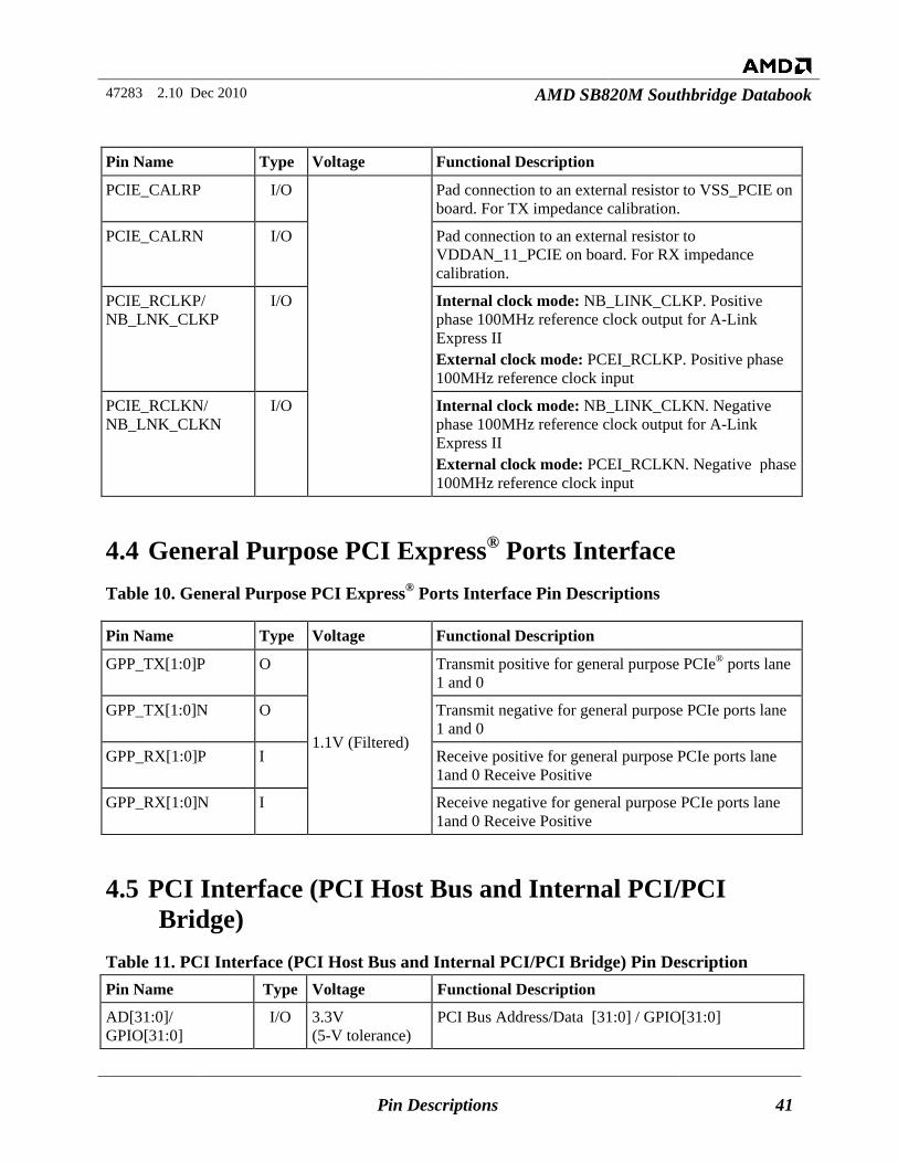
47283 2.10 Dec 2010 AMD SB820M Southbridge Databook
Pin Descriptions 41
Pin Name Type Voltage Functional Description
PCIE_CALRP I/O Pad connection to an external resistor to VSS_PCIE on board. For TX impedance calibration.
PCIE_CALRN I/O Pad connection to an external resistor to VDDAN_11_PCIE on board. For RX impedance calibration.
PCIE_RCLKP/ NB_LNK_CLKP
I/O Internal clock mode: NB_LINK_CLKP. Positive phase 100MHz reference clock output for A-Link Express II External clock mode: PCEI_RCLKP. Positive phase 100MHz reference clock input
PCIE_RCLKN/ NB_LNK_CLKN
I/O Internal clock mode: NB_LINK_CLKN. Negative phase 100MHz reference clock output for A-Link Express II External clock mode: PCEI_RCLKN. Negative phase 100MHz reference clock input
4.4 General Purpose PCI Express® Ports Interface Table 10. General Purpose PCI Express® Ports Interface Pin Descriptions
Pin Name Type Voltage Functional Description
GPP_TX[1:0]P O
1.1V (Filtered)
Transmit positive for general purpose PCIe® ports lane 1 and 0
GPP_TX[1:0]N O Transmit negative for general purpose PCIe ports lane 1 and 0
GPP_RX[1:0]P I Receive positive for general purpose PCIe ports lane 1and 0 Receive Positive
GPP_RX[1:0]N I Receive negative for general purpose PCIe ports lane 1and 0 Receive Positive
4.5 PCI Interface (PCI Host Bus and Internal PCI/PCI Bridge)
Table 11. PCI Interface (PCI Host Bus and Internal PCI/PCI Bridge) Pin Description Pin Name Type Voltage Functional Description
AD[31:0]/ GPIO[31:0]
I/O 3.3V (5-V tolerance)
PCI Bus Address/Data [31:0] / GPIO[31:0]
47283 2.10 Dec 2010 AMD SB820M Southbridge Databook
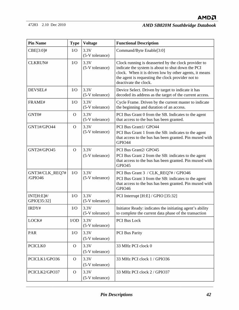
Pin Descriptions 42
Pin Name Type Voltage Functional Description
CBE[3:0]# I/O 3.3V (5-V tolerance)
Command/Byte Enable[3:0]
CLKRUN# I/O 3.3V (5-V tolerance)
Clock running is deasserted by the clock provider to indicate the system is about to shut down the PCI clock. When it is driven low by other agents, it means the agent is requesting the clock provider not to deactivate the clock.
DEVSEL# I/O 3.3V (5-V tolerance)
Device Select. Driven by target to indicate it has decoded its address as the target of the current access.
FRAME# I/O 3.3V (5-V tolerance)
Cycle Frame. Driven by the current master to indicate the beginning and duration of an access.
GNT0# O 3.3V (5-V tolerance)
PCI Bus Grant 0 from the SB. Indicates to the agent that access to the bus has been granted.
GNT1#/GPO44 O 3.3V (5-V tolerance)
PCI Bus Grant1/ GPO44 PCI Bus Grant 1 from the SB: indicates to the agent that access to the bus has been granted. Pin muxed with GPIO44
GNT2#/GPO45 O 3.3V (5-V tolerance)
PCI Bus Grant2/ GPO45 PCI Bus Grant 2 from the SB: indicates to the agent that access to the bus has been granted. Pin muxed with GPIO45
GNT3#/CLK_REQ7#/GPIO46
I/O 3.3V (5-V tolerance)
PCI Bus Grant 3 / CLK_REQ7# / GPIO46 PCI Bus Grant 3 from the SB: indicates to the agent that access to the bus has been granted. Pin muxed with GPIO46
INT[H:E]#/ GPIO[35:32]
I/O 3.3V (5-V tolerance)
PCI Interrupt [H:E] / GPIO [35:32]
IRDY# I/O 3.3V (5-V tolerance)
Initiator Ready: indicates the initiating agent’s ability to complete the current data phase of the transaction
LOCK# I/OD 3.3V (5-V tolerance)
PCI Bus Lock
PAR I/O 3.3V (5-V tolerance)
PCI Bus Parity
PCICLK0 O 3.3V (5-V tolerance)
33 MHz PCI clock 0
PCICLK1/GPO36 O 3.3V (5-V tolerance)
33 MHz PCI clock 1 / GPIO36
PCICLK2/GPO37 O 3.3V (5-V tolerance)
33 MHz PCI clock 2 / GPIO37
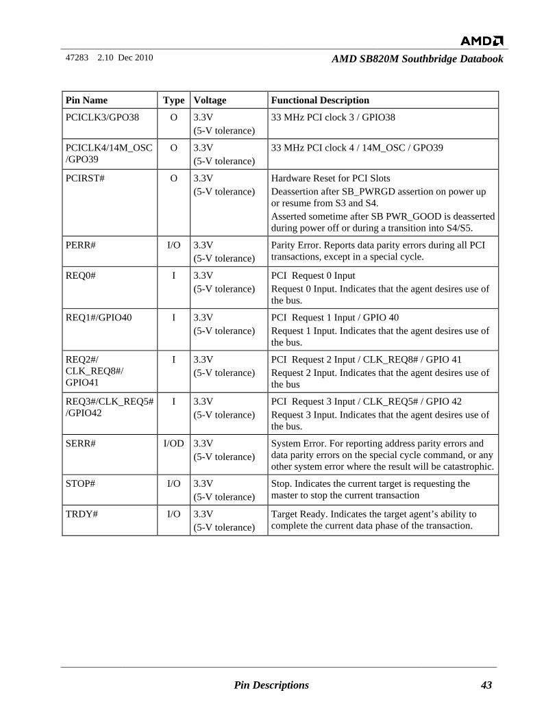
47283 2.10 Dec 2010 AMD SB820M Southbridge Databook
Pin Descriptions 43
Pin Name Type Voltage Functional Description
PCICLK3/GPO38 O 3.3V (5-V tolerance)
33 MHz PCI clock 3 / GPIO38
PCICLK4/14M_OSC/GPO39
O 3.3V (5-V tolerance)
33 MHz PCI clock 4 / 14M_OSC / GPO39
PCIRST# O 3.3V (5-V tolerance)
Hardware Reset for PCI Slots Deassertion after SB_PWRGD assertion on power up or resume from S3 and S4. Asserted sometime after SB PWR_GOOD is deasserted during power off or during a transition into S4/S5.
PERR# I/O 3.3V (5-V tolerance)
Parity Error. Reports data parity errors during all PCI transactions, except in a special cycle.
REQ0# I 3.3V (5-V tolerance)
PCI Request 0 Input Request 0 Input. Indicates that the agent desires use of the bus.
REQ1#/GPIO40 I 3.3V (5-V tolerance)
PCI Request 1 Input / GPIO 40 Request 1 Input. Indicates that the agent desires use of the bus.
REQ2#/ CLK_REQ8#/ GPIO41
I 3.3V (5-V tolerance)
PCI Request 2 Input / CLK_REQ8# / GPIO 41 Request 2 Input. Indicates that the agent desires use of the bus
REQ3#/CLK_REQ5#/GPIO42
I 3.3V (5-V tolerance)
PCI Request 3 Input / CLK_REQ5# / GPIO 42 Request 3 Input. Indicates that the agent desires use of the bus.
SERR# I/OD 3.3V (5-V tolerance)
System Error. For reporting address parity errors and data parity errors on the special cycle command, or any other system error where the result will be catastrophic.
STOP# I/O 3.3V (5-V tolerance)
Stop. Indicates the current target is requesting the master to stop the current transaction
TRDY# I/O 3.3V (5-V tolerance)
Target Ready. Indicates the target agent’s ability to complete the current data phase of the transaction.
47283 2.10 Dec 2010 AMD SB820M Southbridge Databook
Pin Descriptions 44
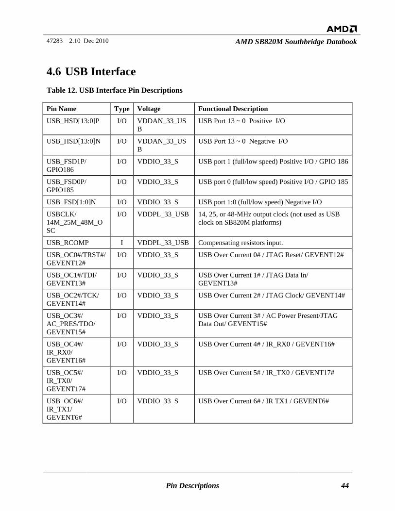
4.6 USB Interface Table 12. USB Interface Pin Descriptions
Pin Name Type Voltage Functional Description
USB_HSD[13:0]P I/O VDDAN_33_USB
USB Port 13 ~ 0 Positive I/O
USB_HSD[13:0]N I/O VDDAN_33_USB
USB Port 13 ~ 0 Negative I/O
USB_FSD1P/ GPIO186
I/O VDDIO_33_S USB port 1 (full/low speed) Positive I/O / GPIO 186
USB_FSD0P/ GPIO185
I/O VDDIO_33_S USB port 0 (full/low speed) Positive I/O / GPIO 185
USB_FSD[1:0]N I/O VDDIO_33_S USB port 1:0 (full/low speed) Negative I/O
USBCLK/ 14M_25M_48M_OSC
I/O VDDPL_33_USB 14, 25, or 48-MHz output clock (not used as USB clock on SB820M platforms)
USB_RCOMP I VDDPL_33_USB Compensating resistors input.
USB_OC0#/TRST#/GEVENT12#
I/O VDDIO_33_S USB Over Current 0# / JTAG Reset/ GEVENT12#
USB_OC1#/TDI/ GEVENT13#
I/O VDDIO_33_S USB Over Current 1# / JTAG Data In/ GEVENT13#
USB_OC2#/TCK/ GEVENT14#
I/O VDDIO_33_S USB Over Current 2# / JTAG Clock/ GEVENT14#
USB_OC3#/ AC_PRES/TDO/ GEVENT15#
I/O VDDIO_33_S USB Over Current 3# / AC Power Present/JTAG Data Out/ GEVENT15#
USB_OC4#/ IR_RX0/ GEVENT16#
I/O VDDIO_33_S USB Over Current 4# / IR_RX0 / GEVENT16#
USB_OC5#/ IR_TX0/ GEVENT17#
I/O VDDIO_33_S USB Over Current 5# / IR_TX0 / GEVENT17#
USB_OC6#/ IR_TX1/ GEVENT6#
I/O VDDIO_33_S USB Over Current 6# / IR TX1 / GEVENT6#
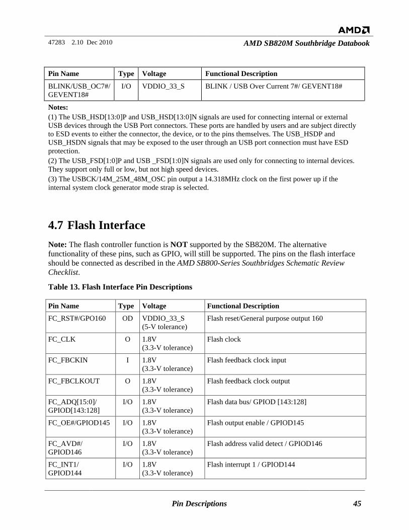
47283 2.10 Dec 2010 AMD SB820M Southbridge Databook
Pin Descriptions 45
Pin Name Type Voltage Functional Description
BLINK/USB_OC7#/ GEVENT18#
I/O VDDIO_33_S BLINK / USB Over Current 7#/ GEVENT18#
Notes: (1) The USB_HSD[13:0]P and USB_HSD[13:0]N signals are used for connecting internal or external USB devices through the USB Port connectors. These ports are handled by users and are subject directly to ESD events to either the connector, the device, or to the pins themselves. The USB_HSDP and USB_HSDN signals that may be exposed to the user through an USB port connection must have ESD protection. (2) The USB_FSD[1:0]P and USB _FSD[1:0]N signals are used only for connecting to internal devices. They support only full or low, but not high speed devices. (3) The USBCK/14M_25M_48M_OSC pin output a 14.318MHz clock on the first power up if the internal system clock generator mode strap is selected.
4.7 Flash Interface Note: The flash controller function is NOT supported by the SB820M. The alternative functionality of these pins, such as GPIO, will still be supported. The pins on the flash interface should be connected as described in the AMD SB800-Series Southbridges Schematic Review Checklist.
Table 13. Flash Interface Pin Descriptions
Pin Name Type Voltage Functional Description
FC_RST#/GPO160 OD VDDIO_33_S (5-V tolerance)
Flash reset/General purpose output 160
FC_CLK O 1.8V (3.3-V tolerance)
Flash clock
FC_FBCKIN I 1.8V (3.3-V tolerance)
Flash feedback clock input
FC_FBCLKOUT O 1.8V (3.3-V tolerance)
Flash feedback clock output
FC_ADQ[15:0]/ GPIOD[143:128]
I/O 1.8V (3.3-V tolerance)
Flash data bus/ GPIOD [143:128]
FC_OE#/GPIOD145 I/O 1.8V (3.3-V tolerance)
Flash output enable / GPIOD145
FC_AVD#/ GPIOD146
I/O 1.8V (3.3-V tolerance)
Flash address valid detect / GPIOD146
FC_INT1/ GPIOD144
I/O 1.8V (3.3-V tolerance)
Flash interrupt 1 / GPIOD144
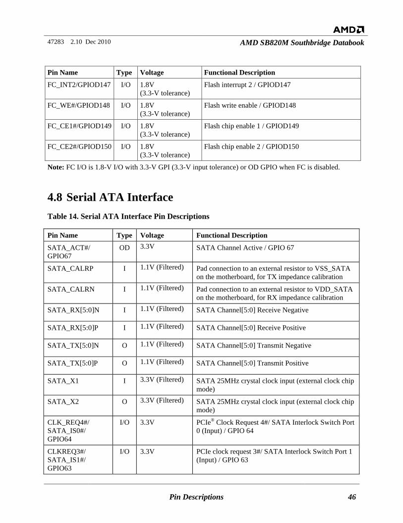
47283 2.10 Dec 2010 AMD SB820M Southbridge Databook
Pin Descriptions 46
Pin Name Type Voltage Functional Description
FC_INT2/GPIOD147 I/O 1.8V (3.3-V tolerance)
Flash interrupt 2 / GPIOD147
FC_WE#/GPIOD148 I/O 1.8V (3.3-V tolerance)
Flash write enable / GPIOD148
FC_CE1#/GPIOD149 I/O 1.8V (3.3-V tolerance)
Flash chip enable 1 / GPIOD149
FC_CE2#/GPIOD150 I/O 1.8V (3.3-V tolerance)
Flash chip enable 2 / GPIOD150
Note: FC I/O is 1.8-V I/O with 3.3-V GPI (3.3-V input tolerance) or OD GPIO when FC is disabled.
4.8 Serial ATA Interface Table 14. Serial ATA Interface Pin Descriptions
Pin Name Type Voltage Functional Description
SATA_ACT#/ GPIO67
OD 3.3V SATA Channel Active / GPIO 67
SATA_CALRP I 1.1V (Filtered) Pad connection to an external resistor to VSS_SATA on the motherboard, for TX impedance calibration
SATA_CALRN I 1.1V (Filtered) Pad connection to an external resistor to VDD_SATA on the motherboard, for RX impedance calibration
SATA_RX[5:0]N I 1.1V (Filtered) SATA Channel[5:0] Receive Negative
SATA_RX[5:0]P I 1.1V (Filtered) SATA Channel[5:0] Receive Positive
SATA_TX[5:0]N O 1.1V (Filtered) SATA Channel[5:0] Transmit Negative
SATA_TX[5:0]P O 1.1V (Filtered) SATA Channel[5:0] Transmit Positive
SATA_X1 I 3.3V (Filtered) SATA 25MHz crystal clock input (external clock chip mode)
SATA_X2 O 3.3V (Filtered) SATA 25MHz crystal clock input (external clock chip mode)
CLK_REQ4#/ SATA_IS0#/ GPIO64
I/O 3.3V PCIe® Clock Request 4#/ SATA Interlock Switch Port 0 (Input) / GPIO 64
CLKREQ3#/ SATA_IS1#/ GPIO63
I/O 3.3V PCIe clock request 3#/ SATA Interlock Switch Port 1 (Input) / GPIO 63
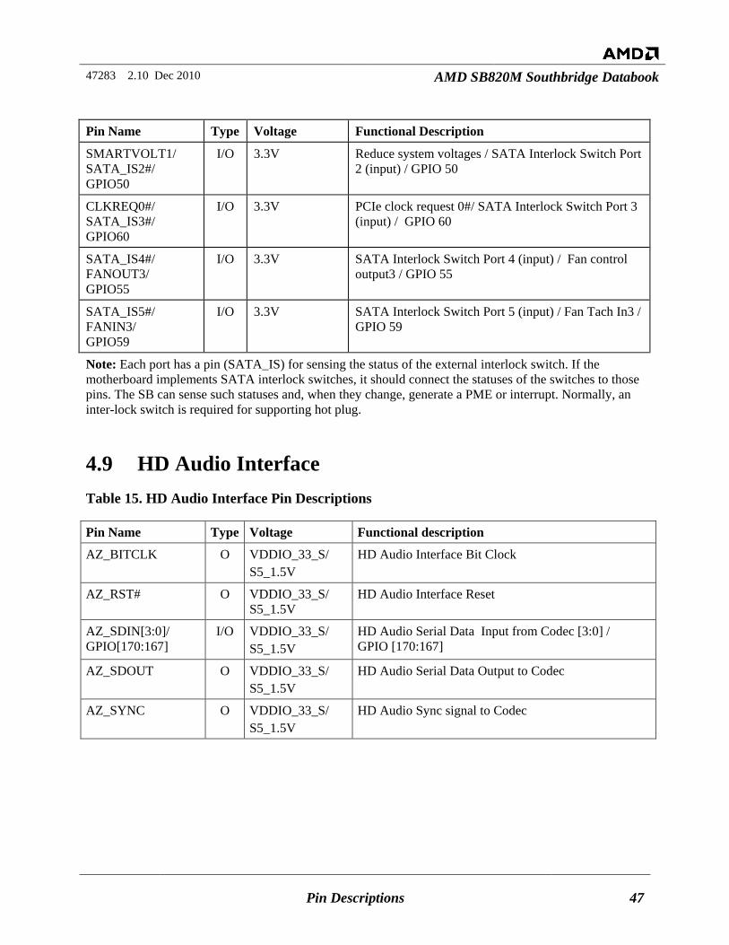
47283 2.10 Dec 2010 AMD SB820M Southbridge Databook
Pin Descriptions 47
Pin Name Type Voltage Functional Description
SMARTVOLT1/ SATA_IS2#/ GPIO50
I/O 3.3V Reduce system voltages / SATA Interlock Switch Port 2 (input) / GPIO 50
CLKREQ0#/ SATA_IS3#/ GPIO60
I/O 3.3V PCIe clock request 0#/ SATA Interlock Switch Port 3 (input) / GPIO 60
SATA_IS4#/ FANOUT3/ GPIO55
I/O 3.3V SATA Interlock Switch Port 4 (input) / Fan control output3 / GPIO 55
SATA_IS5#/ FANIN3/ GPIO59
I/O 3.3V SATA Interlock Switch Port 5 (input) / Fan Tach In3 / GPIO 59
Note: Each port has a pin (SATA_IS) for sensing the status of the external interlock switch. If the motherboard implements SATA interlock switches, it should connect the statuses of the switches to those pins. The SB can sense such statuses and, when they change, generate a PME or interrupt. Normally, an inter-lock switch is required for supporting hot plug.
4.9 HD Audio Interface Table 15. HD Audio Interface Pin Descriptions
Pin Name Type Voltage Functional description
AZ_BITCLK O VDDIO_33_S/ S5_1.5V
HD Audio Interface Bit Clock
AZ_RST# O VDDIO_33_S/ S5_1.5V
HD Audio Interface Reset
AZ_SDIN[3:0]/ GPIO[170:167]
I/O VDDIO_33_S/ S5_1.5V
HD Audio Serial Data Input from Codec [3:0] / GPIO [170:167]
AZ_SDOUT O VDDIO_33_S/ S5_1.5V
HD Audio Serial Data Output to Codec
AZ_SYNC O VDDIO_33_S/ S5_1.5V
HD Audio Sync signal to Codec
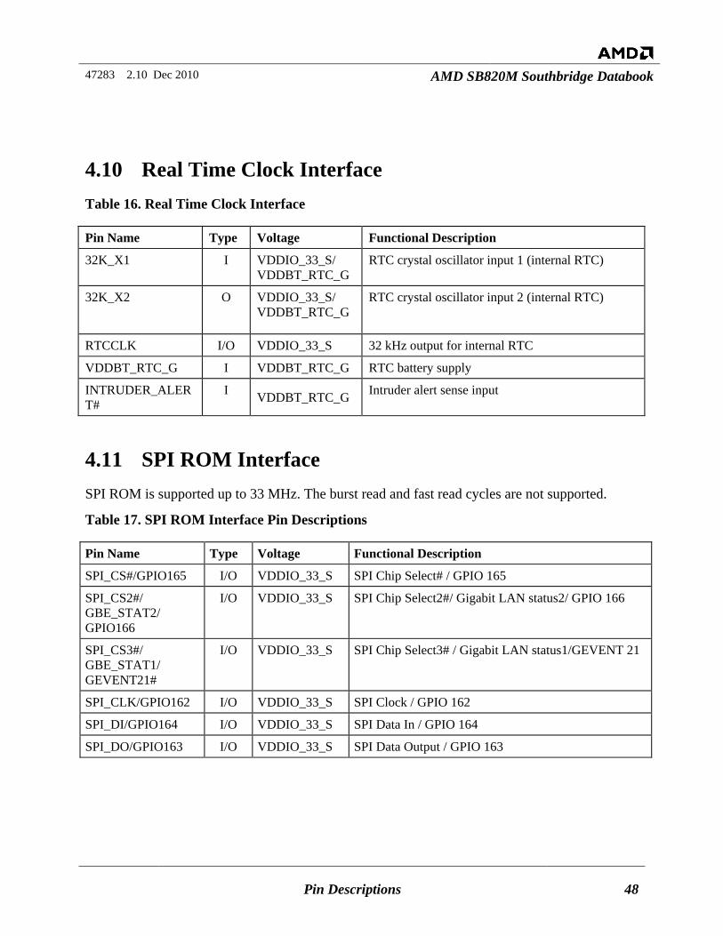
47283 2.10 Dec 2010 AMD SB820M Southbridge Databook
Pin Descriptions 48
4.10 Real Time Clock Interface Table 16. Real Time Clock Interface
Pin Name Type Voltage Functional Description
32K_X1 I VDDIO_33_S/ VDDBT_RTC_G
RTC crystal oscillator input 1 (internal RTC)
32K_X2 O VDDIO_33_S/ VDDBT_RTC_G
RTC crystal oscillator input 2 (internal RTC)
RTCCLK I/O VDDIO_33_S 32 kHz output for internal RTC
VDDBT_RTC_G I VDDBT_RTC_G RTC battery supply
INTRUDER_ALERT#
I VDDBT_RTC_G Intruder alert sense input
4.11 SPI ROM Interface SPI ROM is supported up to 33 MHz. The burst read and fast read cycles are not supported.
Table 17. SPI ROM Interface Pin Descriptions
Pin Name Type Voltage Functional Description
SPI_CS#/GPIO165 I/O VDDIO_33_S SPI Chip Select# / GPIO 165
SPI_CS2#/ GBE_STAT2/ GPIO166
I/O VDDIO_33_S SPI Chip Select2#/ Gigabit LAN status2/ GPIO 166
SPI_CS3#/ GBE_STAT1/ GEVENT21#
I/O VDDIO_33_S SPI Chip Select3# / Gigabit LAN status1/GEVENT 21
SPI_CLK/GPIO162 I/O VDDIO_33_S SPI Clock / GPIO 162
SPI_DI/GPIO164 I/O VDDIO_33_S SPI Data In / GPIO 164
SPI_DO/GPIO163 I/O VDDIO_33_S SPI Data Output / GPIO 163
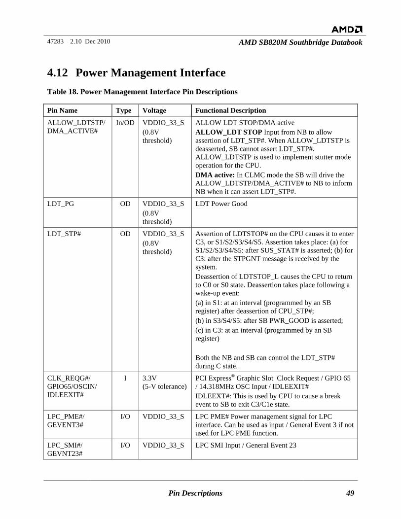
47283 2.10 Dec 2010 AMD SB820M Southbridge Databook
Pin Descriptions 49
4.12 Power Management Interface Table 18. Power Management Interface Pin Descriptions
Pin Name Type Voltage Functional Description
ALLOW_LDTSTP/DMA_ACTIVE#
In/OD VDDIO_33_S (0.8V threshold)
ALLOW LDT STOP/DMA active ALLOW_LDT STOP Input from NB to allow assertion of LDT_STP#. When ALLOW_LDTSTP is deasserted, SB cannot assert LDT_STP#. ALLOW_LDTSTP is used to implement stutter mode operation for the CPU. DMA active: In CLMC mode the SB will drive the ALLOW_LDTSTP/DMA_ACTIVE# to NB to inform NB when it can assert LDT_STP#.
LDT_PG OD VDDIO_33_S (0.8V threshold)
LDT Power Good
LDT_STP# OD VDDIO_33_S (0.8V threshold)
Assertion of LDTSTOP# on the CPU causes it to enter C3, or S1/S2/S3/S4/S5. Assertion takes place: (a) for S1/S2/S3/S4/S5: after SUS_STAT# is asserted; (b) for C3: after the STPGNT message is received by the system. Deassertion of LDTSTOP_L causes the CPU to return to C0 or S0 state. Deassertion takes place following a wake-up event: (a) in S1: at an interval (programmed by an SB register) after deassertion of CPU_STP#; (b) in S3/S4/S5: after SB PWR_GOOD is asserted; (c) in C3: at an interval (programmed by an SB register) Both the NB and SB can control the LDT_STP# during C state.
CLK_REQG#/ GPIO65/OSCIN/ IDLEEXIT#
I 3.3V (5-V tolerance)
PCI Express® Graphic Slot Clock Request / GPIO 65 / 14.318MHz OSC Input / IDLEEXIT# IDLEEXT#: This is used by CPU to cause a break event to SB to exit C3/C1e state.
LPC_PME#/ GEVENT3#
I/O VDDIO_33_S LPC PME# Power management signal for LPC interface. Can be used as input / General Event 3 if not used for LPC PME function.
LPC_SMI#/ GEVNT23#
I/O VDDIO_33_S LPC SMI Input / General Event 23
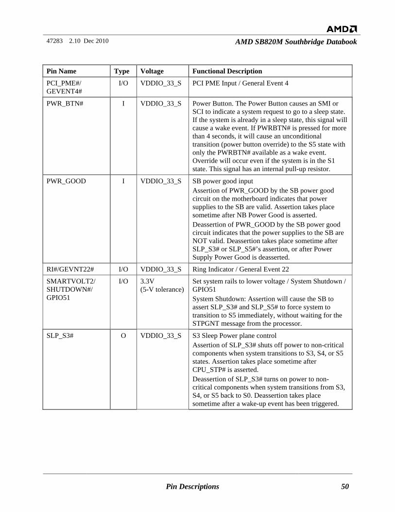
47283 2.10 Dec 2010 AMD SB820M Southbridge Databook
Pin Descriptions 50
Pin Name Type Voltage Functional Description
PCI_PME#/ GEVENT4#
I/O VDDIO_33_S PCI PME Input / General Event 4
PWR_BTN# I VDDIO_33_S
Power Button. The Power Button causes an SMI or SCI to indicate a system request to go to a sleep state. If the system is already in a sleep state, this signal will cause a wake event. If PWRBTN# is pressed for more than 4 seconds, it will cause an unconditional transition (power button override) to the S5 state with only the PWRBTN# available as a wake event. Override will occur even if the system is in the S1 state. This signal has an internal pull-up resistor.
PWR_GOOD I VDDIO_33_S SB power good input Assertion of PWR_GOOD by the SB power good circuit on the motherboard indicates that power supplies to the SB are valid. Assertion takes place sometime after NB Power Good is asserted. Deassertion of PWR_GOOD by the SB power good circuit indicates that the power supplies to the SB are NOT valid. Deassertion takes place sometime after SLP_S3# or SLP_S5#’s assertion, or after Power Supply Power Good is deasserted.
RI#/GEVNT22# I/O VDDIO_33_S Ring Indicator / General Event 22
SMARTVOLT2/ SHUTDOWN#/ GPIO51
I/O 3.3V (5-V tolerance)
Set system rails to lower voltage / System Shutdown / GPIO51 System Shutdown: Assertion will cause the SB to assert SLP_S3# and SLP_S5# to force system to transition to S5 immediately, without waiting for the STPGNT message from the processor.
SLP_S3# O VDDIO_33_S
S3 Sleep Power plane control Assertion of SLP_S3# shuts off power to non-critical components when system transitions to S3, S4, or S5 states. Assertion takes place sometime after CPU_STP# is asserted. Deassertion of SLP_S3# turns on power to non-critical components when system transitions from S3, S4, or S5 back to S0. Deassertion takes place sometime after a wake-up event has been triggered.
47283 2.10 Dec 2010 AMD SB820M Southbridge Databook
Pin Descriptions 51
Pin Name Type Voltage Functional Description
SLP_S5# O VDDIO_33_S S5 Sleep Power plane control - Assertion of SLP_S5# shuts power off to non-critical components when system transitions to S4 or S5 state. Assertion takes place sometime after CPU_STP# is asserted. Deassertion of SLP_S5# turns on power to non-critical components when transitioning from S4/S5 back to S0 state. Deassertion takes place sometime after a wake-up event is triggered.
THRMTRIP#/ SMBALERT#/ GEVENT2#
I/O VDDIO_33_S Thermal Trip / SMBus Alert / General Event 2 Thermal Trip: Signal indicates to the SB that a thermal trip has occurred. Its assertion will cause the SB to transition the system to S5 immediately, without waiting for the STPGNT message from the processor.
SUS_STAT# OD
VDDIO_33_S Suspend Status – Assertion by the SB indicates that the system will be entering a low-power state soon. The signal is monitored by those devices with memory that needs to switch from normal refresh to suspend refresh mode when the system transitions to a low-power state. Assertion takes place after the Stop Grant message from the CPU is received by the system. Deassertion by the SB indicates that the system is exiting a low power state now and is returning to S0. Deassertion takes place after LDT_STP# is deasserted.
TEMPIN3/ TALERT#/ GPIO174
I/O VDDIO_33_S Temperature Monitor Input 3/ Thermal Alert / GPIO 174 Thermal Alert: The signal is a thermal alert to the SB. SB can be programmed to generate an SMI, SCI, or IRQ13 through GPE, or generate an SMI without GPE in response to the signal’s assertion. See the AMD SB800-Series Southbridges Register Reference Guide (PID# 45482) for details.
47283 2.10 Dec 2010 AMD SB820M Southbridge Databook
Pin Descriptions 52
Pin Name Type Voltage Functional Description
WAKE#/ GEVENT8#
I/O VDDIO_33_S PCI Express® Wake /General Event 8
PCI Express Wake: On Power up this pin will function as WAKE# in legacy mode. Optionally, WAKE# in native mode can be enabled after power up, only by software. When the pin is asserted (active low) the Southbridge will generate the wake event. The WAKE# function is supported in S5 through S0, with the following restriction:
Wake function in S5 state—When transitioning from G3 to S5, the WAKE# function will not be enabled. However, after an initial transition from S5 to S0 and back to S5, the WAKE# function will be enabled. It will stay enabled for any subsequent transition from S0 to S5.
Care must be taken when plugging in PCIe® devices. The system should be transitioned into the G3 state (S5 power off) before a PCIe device is installed. Plugging in a PCIe device when the system is in S5 state may cause the system to wake up, because the WAKE# signal driven by the PCIe device may transition momentarily to the active state when the device is installed but has not been initialized to drive the signal in an inactive state.
NB_PWRGD OD 3.3V Northbridge Power good
4.13 SMBus Interface Table 19. SMBus Interface Pin Descriptions
Pin Name Type Voltage Functional Description
SCL0/GPIO43 I/OD 3.3V (5-V tolerance)
SMBus Clock 0 / GPIO 43 Note: Pin type is I/O when configured as GPIO.
SDA0/GPIO47 I/OD 3.3V (5-V tolerance)
SMBus Data 0 / GPIO 47 Note: Pin type is I/O when configured as GPIO.
SCL1/GPIO227 I/OD VDDIO_33_S SMBus Clock 1 / GPIO 227 This SMBus Clock is for supporting an ASF interface. Note: Pin type is I/O when configured as GPIO.
SDA1/GPIO228 I/OD VDDIO_33_S SMBus Data 1 / GPIO 228 This SMBus Data is for supporting an ASF interface. Note: Pin type is I/O when configured as GPIO.
47283 2.10 Dec 2010 AMD SB820M Southbridge Databook
Pin Descriptions 53
Pin Name Type Voltage Functional Description
SCL2/GPIO193 I/OD VDDIO_33_S SMBus Clock 2/GPIO 193 Note: Pin type is I/O when configured as GPIO.
SDA2/GPIO194 I/OD VDDIO_33_S SMBus Data 2/GPIO 194 Note: Pin type is I/O when configured as GPIO.
SCL3_LV/GPIO195 I/OD VDDIO_33_S domain (0.8V threshold)
SMBus Clock 3/GPIO 195 Note: Pin type is I/O when configured as GPIO.
SDA3_LV/GPIO196 I/OD VDDIO_33_S domain (0.8V threshold)
SMBus Data 3/GPIO 196 Note: Pin type is I/O when configured as GPIO.
PS2_CLK/SCL4/ GPIO188
I/OD VDDIO_33_S Aux PS2 Clock / SMBus Clock 4/GPIO 188 Note: Pin type is I/O when configured as GPIO.
PS2_DAT/SDA4/ GPIO187
I /OD VDDIO_33_S Aux PS2 Data / SMBus Data 4/GPIO 184 Note: Pin type is I/O when configured as GPIO.
THRMTRIP#/ SMBALERT#/ GEVENT2#
I/O VDDIO_33_S Thermal Trip / SMBus Alert# / General Event 2 SM Bus Alert: This signal is used to wake the system or generate an SMI. If not used for SMBALERT#, it can be used for thermal trip or as a GEVENT.
Note: (1) The SDA1 and SCL1 SMBus interface is dedicated for ASF devices only. It should not be used to connect to any other devices. (2) There are only two SMBus controllers. The SCL1/SDA1 pair is controlled by SMBus controller 1. SCL0/SDA0, SCL2/SDA2, SCL3/SDA3 and SCL4/SDA4 are multiplexed pins that are all controlled by SMBus controller 0, and only 1 pair of those pins can be active at any time.
4.14 Reset / Clocks / ATE / JTAG Table 20. Reset/Clocks/ATE/JTAG Interface Pin Descriptions
Pin Name Type Voltage Functional Description
A_RST# O VDDIO_33_S PCI Host Bus Reset. Asserted during transition to S3/S4/S5 to reset all devices in the SB or connected to it, except the ACPI logic in the SB.
AZ_RST# O VDDIO_33_S/ S5_1.5V HD Audio interface Reset
DDR3_RST#/ GEVENT7#
OD VDDIO_33_S System Memory Reset /General Event 7
47283 2.10 Dec 2010 AMD SB820M Southbridge Databook
Pin Descriptions 54
Pin Name Type Voltage Functional Description
FC_RST#/GPO160 OD VDDIO_33_S Flash Reset / General purpose output 160
GBE_PHY_RST# O VDDIO_33_S Gigabit PHY Reset
LDT_RST# OD VDDIO_33_S (0.8V threshold)
LDT Reset#. Reset signal to the CPU. Assertion of LDT_RST# causes the CPU to transition into a low power state and to deassert MEMCLKEA/B and assert MEMREST_L. Assertion of LDT_RST# takes place sometime after SB PWRGOOD has been deasserted. Deassertion of LDT_RST# allows MEMRESET_L to be deasserted and MEMCLK to be enabled. Deassertion of LDT_RST# takes place sometime after SB PWR_GOOD has been asserted.
PCIE_RST# O VDDIO_33_S PCIe® Reset. Asserted during transition to S3/S4/S5.
PCIRST# O 3.3 V (5-V Tolerance)
Hardware Reset for PCI Slots Assertion: (a) at power on, (b) sometime after CPU_STP#’s assertion in S0, (c) after the system has transitioned into S4/S5. Deassertion: sometime after SB PWR_GOOD is asserted during power on or during a transition from S4/S5 to S0.
ROM_RST#/ GPIO161
I/O VDDIO_33_S ROM Reset / GPIO 161 ROM Reset : Early version of system reset, the deassertion of which is ahead of other system reset signals such as A_RST#, PCIE_RST#, or PCIRST#. Used for resetting the system BIOS flash ROM.
RSMRST# I VDDIO_33_S Resume Reset from Motherboard – Assertion of RSMRST# resets all SB registers to their default values. It also causes all reset signals originating from the SB (A_RST#, PCIRST#, PCIE_RST#, LDT_RST#, AZ_RST#, FC_RST#, GBE_PHY_RST#, ROM_RST# and, DDR3_RST#) to be issued. RSRMT# should be asserted when system power is being applied first time. RSMRST# should be deasserted sometime after S5 power is up, and should stay deasserted until system power is removed.
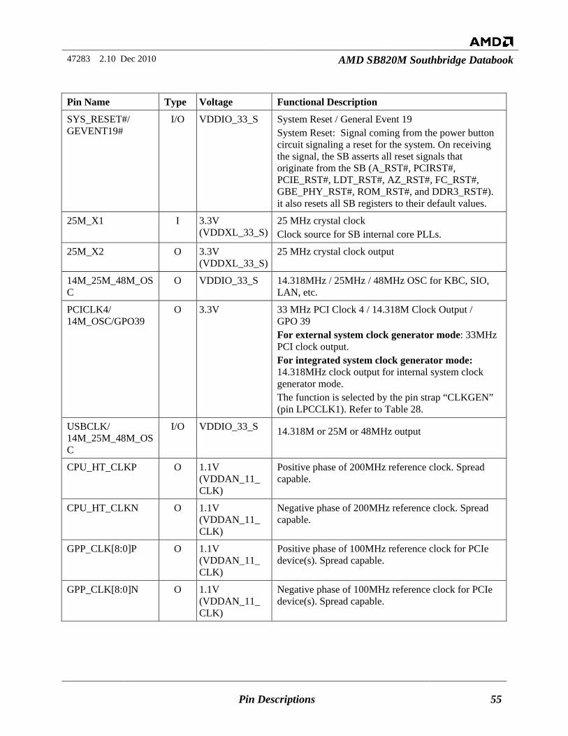
47283 2.10 Dec 2010 AMD SB820M Southbridge Databook
Pin Descriptions 55
Pin Name Type Voltage Functional Description
SYS_RESET#/ GEVENT19#
I/O VDDIO_33_S System Reset / General Event 19 System Reset: Signal coming from the power button circuit signaling a reset for the system. On receiving the signal, the SB asserts all reset signals that originate from the SB (A_RST#, PCIRST#, PCIE_RST#, LDT_RST#, AZ_RST#, FC_RST#, GBE_PHY_RST#, ROM_RST#, and DDR3_RST#). it also resets all SB registers to their default values.
25M_X1 I 3.3V (VDDXL_33_S)
25 MHz crystal clock Clock source for SB internal core PLLs.
25M_X2 O 3.3V (VDDXL_33_S)
25 MHz crystal clock output
14M_25M_48M_OSC
O VDDIO_33_S 14.318MHz / 25MHz / 48MHz OSC for KBC, SIO, LAN, etc.
PCICLK4/ 14M_OSC/GPO39
O 3.3V 33 MHz PCI Clock 4 / 14.318M Clock Output / GPO 39 For external system clock generator mode: 33MHz PCI clock output. For integrated system clock generator mode: 14.318MHz clock output for internal system clock generator mode. The function is selected by the pin strap “CLKGEN” (pin LPCCLK1). Refer to Table 28.
USBCLK/ 14M_25M_48M_OSC
I/O VDDIO_33_S 14.318M or 25M or 48MHz output
CPU_HT_CLKP O 1.1V (VDDAN_11_ CLK)
Positive phase of 200MHz reference clock. Spread capable.
CPU_HT_CLKN O 1.1V (VDDAN_11_ CLK)
Negative phase of 200MHz reference clock. Spread capable.
GPP_CLK[8:0]P O 1.1V (VDDAN_11_ CLK)
Positive phase of 100MHz reference clock for PCIe device(s). Spread capable.
GPP_CLK[8:0]N O 1.1V (VDDAN_11_ CLK)
Negative phase of 100MHz reference clock for PCIe device(s). Spread capable.
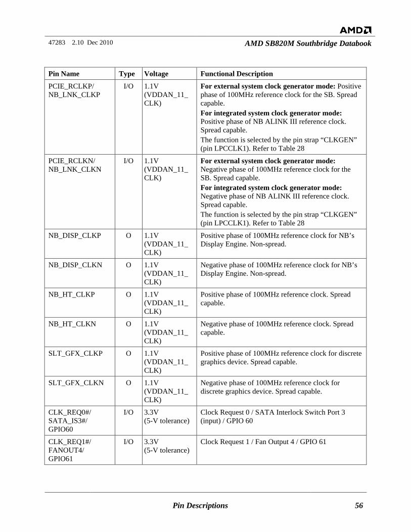
47283 2.10 Dec 2010 AMD SB820M Southbridge Databook
Pin Descriptions 56
Pin Name Type Voltage Functional Description
PCIE_RCLKP/ NB_LNK_CLKP
I/O 1.1V (VDDAN_11_ CLK)
For external system clock generator mode: Positive phase of 100MHz reference clock for the SB. Spread capable. For integrated system clock generator mode: Positive phase of NB ALINK III reference clock. Spread capable. The function is selected by the pin strap “CLKGEN” (pin LPCCLK1). Refer to Table 28
PCIE_RCLKN/ NB_LNK_CLKN
I/O 1.1V (VDDAN_11_ CLK)
For external system clock generator mode: Negative phase of 100MHz reference clock for the SB. Spread capable. For integrated system clock generator mode: Negative phase of NB ALINK III reference clock. Spread capable. The function is selected by the pin strap “CLKGEN” (pin LPCCLK1). Refer to Table 28
NB_DISP_CLKP O 1.1V (VDDAN_11_ CLK)
Positive phase of 100MHz reference clock for NB’s Display Engine. Non-spread.
NB_DISP_CLKN O 1.1V (VDDAN_11_ CLK)
Negative phase of 100MHz reference clock for NB’s Display Engine. Non-spread.
NB_HT_CLKP O 1.1V (VDDAN_11_ CLK)
Positive phase of 100MHz reference clock. Spread capable.
NB_HT_CLKN O 1.1V (VDDAN_11_ CLK)
Negative phase of 100MHz reference clock. Spread capable.
SLT_GFX_CLKP O 1.1V (VDDAN_11_ CLK)
Positive phase of 100MHz reference clock for discrete graphics device. Spread capable.
SLT_GFX_CLKN O 1.1V (VDDAN_11_ CLK)
Negative phase of 100MHz reference clock for discrete graphics device. Spread capable.
CLK_REQ0#/ SATA_IS3#/ GPIO60
I/O 3.3V (5-V tolerance)
Clock Request 0 / SATA Interlock Switch Port 3 (input) / GPIO 60
CLK_REQ1#/ FANOUT4/ GPIO61
I/O 3.3V (5-V tolerance)
Clock Request 1 / Fan Output 4 / GPIO 61
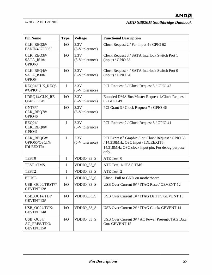
47283 2.10 Dec 2010 AMD SB820M Southbridge Databook
Pin Descriptions 57
Pin Name Type Voltage Functional Description
CLK_REQ2#/ FANIN4/GPIO62
I/O 3.3V (5-V tolerance)
Clock Request 2 / Fan Input 4 / GPIO 62
CLK_REQ3#/ SATA_IS1#/ GPIO63
I/O 3.3V (5-V tolerance)
Clock Request 3 / SATA Interlock Switch Port 1 (input) / GPIO 63
CLK_REQ4#/ SATA_IS0#/ GPIO64
I/O 3.3V (5-V tolerance)
Clock Request 4 / SATA Interlock Switch Port 0 (input) / GPIO 64
REQ3#/CLK_REQ5#/GPIO42
I 3.3V (5-V tolerance)
PCI Request 3 / Clock Request 5 / GPIO 42
LDRQ1#/CLK_REQ6#/GPIO49
I/O 3.3V (5-V tolerance)
Encoded DMA Bus Master Request 1/Clock Request 6 / GPIO 49
GNT3#/ CLK_REQ7#/ GPIO46
I/O 3.3V (5-V tolerance)
PCI Grant 3 / Clock Request 7 / GPIO 46
REQ2#/ CLK_REQ8#/ GPIO41
I 3.3V (5-V tolerance)
PCI Request 2 / Clock Request 8 / GPIO 41
CLK_REQG#/ GPIO65/OSCIN/ IDLEEXIT#
I 3.3V (5-V tolerance)
PCI Express® Graphic Slot Clock Request / GPIO 65 / 14.318MHz OSC Input / IDLEEXIT# 14.318MHz OSC clock input pin. For debug purpose only.
TEST0 I VDDIO_33_S ATE Test 0
TEST1/TMS I VDDIO_33_S ATE Test 1/ JTAG TMS
TEST2 I VDDIO_33_S ATE Test 2
EFUSE I VDDIO_33_S Efuse. Pull to GND on motherboard.
USB_OC0#/TRST#/ GEVENT12#
I/O VDDIO_33_S USB Over Current 0# / JTAG Reset/ GEVENT 12
USB_OC1#/TDI/ GEVENT13#
I/O VDDIO_33_S USB Over Current 1# / JTAG Data In/ GEVENT 13
USB_OC2#/TCK/ GEVENT14#
I/O VDDIO_33_S USB Over Current 2# / JTAG Clock/ GEVENT 14
USB_OC3#/ AC_PRES/TDO/ GEVENT15#
I/O VDDIO_33_S USB Over Current 3# / AC Power Present/JTAG Data Out/ GEVENT 15
47283 2.10 Dec 2010 AMD SB820M Southbridge Databook
Pin Descriptions 58
4.15 General Purpose I/O and General Event The GPIO and GEVENT pins of the SB are multiplexed with other functions. For information on how to configure the GPIO pins for the desired functions, see the AMD SB800-Series Southbridges Register Reference Guide (PID# 45482).
Table 21 lists all the GPIO and GEVENT pins on the SB. The Default I/O State column shows the direction and the state of the pin after the core power has become stable (VDDCR > ~0.8V). The integrated resistor column shows the default status of the internal integrated pull-up/pull-down resistor on the pin after the PCI host bus reset (A_RST#) is deasserted. The integrated resistor can be enabled/disabled by system BIOS after boot up.
Notes: 1. Certain GPIOs are multiplexed with pins on the flash controller, keyboard and PS/2 controller, or Gigabit Ethernet Media Access Controller (GbE MAC) interfaces. The flash controller, keyboard and PS/2 controller, and GbE MAC functions are NOT supported by the SB, and pin name prefixes like “FC,” “GbE,” or “PS2” do not imply availability of those functions. 2. The voltage monitor function is NOT supported by the SB. The “VIN” prefix of certain GPIOs does not imply availability of the VIN function. 3. GPIO[35:0] can only be used if the PCI interface is not used and is disabled by programming the PM register EAh bit 0 to 1.
Table 21. General Purpose I/O and General Event Pin Descriptions
System Pin Name Type Level Default Muxed
Function
Default I/O
State
Inte-grated
Resistor Functional Descriptions
General Events
GA20IN/GEVENT0# I 3.3V (5-V
tolerance)
null Input, PU 8.2K PU A20Gate input from SIO / General Event 0
KBRST#/ GEVENT1#
I 3.3V (5-V
tolerance)
KBRST# Input, PU 8.2K PU Keyboard Reset / General Event 1 Note: On G3 to S5 transition, the BIOS will not be able to program this pin as Gevent1#. If the pin is used as Gevent1#, the design should ensure that the pin remains in logical high during the G3 S5 S0 transition. BIOS can then program this pin as Gevent1# when it is posting.
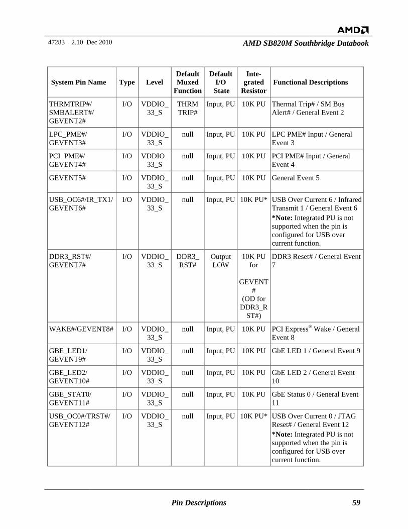
47283 2.10 Dec 2010 AMD SB820M Southbridge Databook
Pin Descriptions 59
System Pin Name Type Level Default Muxed
Function
Default I/O
State
Inte-grated
Resistor Functional Descriptions
THRMTRIP#/ SMBALERT#/ GEVENT2#
I/O VDDIO_33_S
THRM TRIP#
Input, PU 10K PU Thermal Trip# / SM Bus Alert# / General Event 2
LPC_PME#/ GEVENT3#
I/O VDDIO_33_S
null Input, PU 10K PU LPC PME# Input / General Event 3
PCI_PME#/ GEVENT4#
I/O VDDIO_33_S
null Input, PU 10K PU PCI PME# Input / General Event 4
GEVENT5# I/O VDDIO_33_S
null Input, PU 10K PU
General Event 5
USB_OC6#/IR_TX1/GEVENT6#
I/O VDDIO_33_S
null Input, PU 10K PU* USB Over Current 6 / Infrared Transmit 1 / General Event 6 *Note: Integrated PU is not supported when the pin is configured for USB over current function.
DDR3_RST#/ GEVENT7#
I/O VDDIO_33_S
DDR3_ RST#
Output LOW
10K PU for
GEVENT
# (OD for
DDR3_RST#)
DDR3 Reset# / General Event 7
WAKE#/GEVENT8# I/O VDDIO_33_S
null Input, PU 10K PU PCI Express® Wake / General Event 8
GBE_LED1/ GEVENT9#
I/O VDDIO_33_S
null Input, PU 10K PU GbE LED 1 / General Event 9
GBE_LED2/ GEVENT10#
I/O VDDIO_33_S
null Input, PU 10K PU GbE LED 2 / General Event 10
GBE_STAT0/ GEVENT11#
I/O VDDIO_33_S
null Input, PU 10K PU GbE Status 0 / General Event 11
USB_OC0#/TRST#/GEVENT12#
I/O VDDIO_33_S
null Input, PU 10K PU* USB Over Current 0 / JTAG Reset# / General Event 12 *Note: Integrated PU is not supported when the pin is configured for USB over current function.
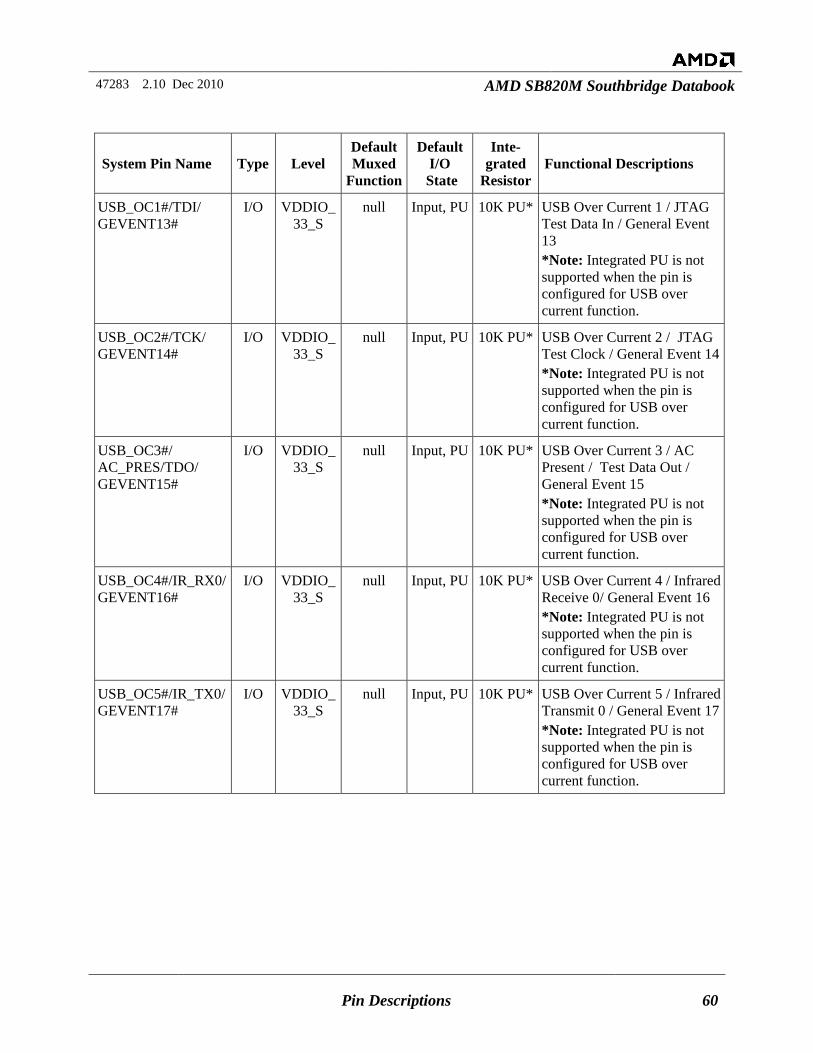
47283 2.10 Dec 2010 AMD SB820M Southbridge Databook
Pin Descriptions 60
System Pin Name Type Level Default Muxed
Function
Default I/O
State
Inte-grated
Resistor Functional Descriptions
USB_OC1#/TDI/ GEVENT13#
I/O VDDIO_33_S
null Input, PU 10K PU* USB Over Current 1 / JTAG Test Data In / General Event 13 *Note: Integrated PU is not supported when the pin is configured for USB over current function.
USB_OC2#/TCK/ GEVENT14#
I/O VDDIO_33_S
null Input, PU 10K PU* USB Over Current 2 / JTAG Test Clock / General Event 14 *Note: Integrated PU is not supported when the pin is configured for USB over current function.
USB_OC3#/ AC_PRES/TDO/ GEVENT15#
I/O VDDIO_33_S
null Input, PU 10K PU* USB Over Current 3 / AC Present / Test Data Out / General Event 15 *Note: Integrated PU is not supported when the pin is configured for USB over current function.
USB_OC4#/IR_RX0/GEVENT16#
I/O VDDIO_33_S
null Input, PU 10K PU* USB Over Current 4 / Infrared Receive 0/ General Event 16 *Note: Integrated PU is not supported when the pin is configured for USB over current function.
USB_OC5#/IR_TX0/GEVENT17#
I/O VDDIO_33_S
null Input, PU 10K PU* USB Over Current 5 / Infrared Transmit 0 / General Event 17 *Note: Integrated PU is not supported when the pin is configured for USB over current function.
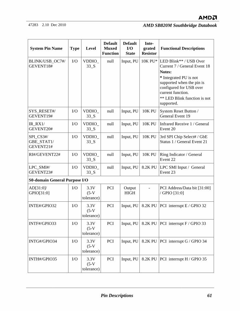
47283 2.10 Dec 2010 AMD SB820M Southbridge Databook
Pin Descriptions 61
System Pin Name Type Level Default Muxed
Function
Default I/O
State
Inte-grated
Resistor Functional Descriptions
BLINK/USB_OC7#/GEVENT18#
I/O VDDIO_33_S
null Input, PU 10K PU* LED Blink** / USB Over Current 7 / General Event 18 Notes: * Integrated PU is not supported when the pin is configured for USB over current function. ** LED Blink function is not supported.
SYS_RESET#/ GEVENT19#
I/O VDDIO_33_S
null Input, PU 10K PU System Reset Button / General Event 19
IR_RX1/ GEVENT20#
I/O VDDIO_33_S
null Input, PU 10K PU Infrared Receive 1 / General Event 20
SPI_CS3#/ GBE_STAT1/ GEVENT21#
I/O VDDIO_33_S
null Input, PU 10K PU 3rd SPI Chip Select# / GbE Status 1 / General Event 21
RI#/GEVENT22# I/O VDDIO_33_S
null Input, PU 10K PU Ring Indicator / General Event 22
LPC_SMI#/ GEVENT23#
I/O VDDIO_33_S
null Input, PU 8.2K PU LPC SMI Input / General Event 23
S0-domain General Purpose I/O
AD[31:0]/ GPIO[31:0]
I/O 3.3V (5-V
tolerance)
PCI Output HIGH
- PCI Address/Data bit [31:00] / GPIO [31:0]
INTE#/GPIO32 I/O 3.3V (5-V
tolerance)
PCI Input, PU 8.2K PU PCI interrupt E / GPIO 32
INTF#/GPIO33 I/O 3.3V (5-V
tolerance)
PCI Input, PU 8.2K PU PCI interrupt F / GPIO 33
INTG#/GPIO34 I/O 3.3V (5-V
tolerance)
PCI Input, PU 8.2K PU PCI interrupt G / GPIO 34
INTH#/GPIO35 I/O 3.3V (5-V
tolerance)
PCI Input, PU 8.2K PU PCI interrupt H / GPIO 35
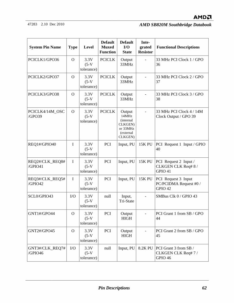
47283 2.10 Dec 2010 AMD SB820M Southbridge Databook
Pin Descriptions 62
System Pin Name Type Level Default Muxed
Function
Default I/O
State
Inte-grated
Resistor Functional Descriptions
PCICLK1/GPO36 O 3.3V (5-V
tolerance)
PCICLK Output 33MHz
- 33 MHz PCI Clock 1 / GPO 36
PCICLK2/GPO37 O 3.3V (5-V
tolerance)
PCICLK Output 33MHz
- 33 MHz PCI Clock 2 / GPO 37
PCICLK3/GPO38 O 3.3V (5-V
tolerance)
PCICLK Output 33MHz
- 33 MHz PCI Clock 3 / GPO 38
PCICLK4/14M_OSC/GPO39
O 3.3V (5-V
tolerance)
PCICLK Output 14MHz (internal
CLKGEN) or 33MHz (external
CLKGEN)
- 33 MHz PCI Clock 4 / 14M Clock Output / GPO 39
REQ1#/GPIO40 I 3.3V (5-V
tolerance)
PCI Input, PU 15K PU PCI Request 1 Input / GPIO 40
REQ2#/CLK_REQ8#/GPIO41
I 3.3V (5-V
tolerance)
PCI Input, PU 15K PU PCI Request 2 Input / CLKGEN CLK Req# 8 / GPIO 41
REQ3#/CLK_REQ5#/GPIO42
I 3.3V (5-V
tolerance)
PCI Input, PU 15K PU PCI Request 3 Input PC/PCIDMA Request #0 / GPIO 42
SCL0/GPIO43 I/O 3.3V (5-V
tolerance)
null Input, Tri-State
- SMBus Clk 0 / GPIO 43
GNT1#/GPO44 O 3.3V (5-V
tolerance)
PCI Output HIGH
- PCI Grant 1 from SB / GPO 44
GNT2#/GPO45 O 3.3V (5-V
tolerance)
PCI Output HIGH
- PCI Grant 2 from SB / GPO 45
GNT3#/CLK_REQ7#/GPIO46
I/O 3.3V (5-V
tolerance)
null Input, PU 8.2K PU PCI Grant 3 from SB / CLKGEN CLK Req# 7 / GPIO 46
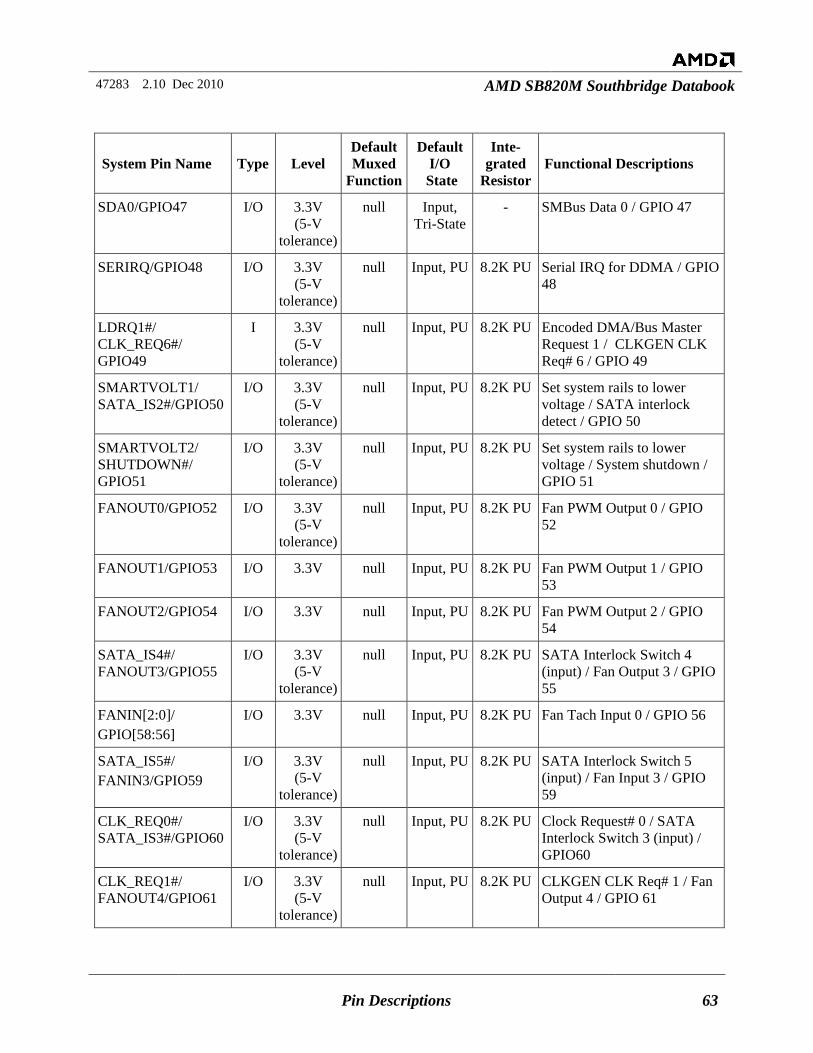
47283 2.10 Dec 2010 AMD SB820M Southbridge Databook
Pin Descriptions 63
System Pin Name Type Level Default Muxed
Function
Default I/O
State
Inte-grated
Resistor Functional Descriptions
SDA0/GPIO47 I/O 3.3V (5-V
tolerance)
null Input, Tri-State
- SMBus Data 0 / GPIO 47
SERIRQ/GPIO48 I/O 3.3V (5-V
tolerance)
null Input, PU 8.2K PU Serial IRQ for DDMA / GPIO 48
LDRQ1#/ CLK_REQ6#/ GPIO49
I 3.3V (5-V
tolerance)
null Input, PU 8.2K PU Encoded DMA/Bus Master Request 1 / CLKGEN CLK Req# 6 / GPIO 49
SMARTVOLT1/ SATA_IS2#/GPIO50
I/O 3.3V (5-V
tolerance)
null Input, PU 8.2K PU Set system rails to lower voltage / SATA interlock detect / GPIO 50
SMARTVOLT2/ SHUTDOWN#/ GPIO51
I/O 3.3V (5-V
tolerance)
null Input, PU 8.2K PU Set system rails to lower voltage / System shutdown / GPIO 51
FANOUT0/GPIO52 I/O 3.3V (5-V
tolerance)
null Input, PU 8.2K PU Fan PWM Output 0 / GPIO 52
FANOUT1/GPIO53 I/O 3.3V null Input, PU 8.2K PU Fan PWM Output 1 / GPIO 53
FANOUT2/GPIO54 I/O 3.3V null Input, PU 8.2K PU Fan PWM Output 2 / GPIO 54
SATA_IS4#/ FANOUT3/GPIO55
I/O 3.3V (5-V
tolerance)
null Input, PU 8.2K PU SATA Interlock Switch 4 (input) / Fan Output 3 / GPIO 55
FANIN[2:0]/ GPIO[58:56]
I/O 3.3V null Input, PU 8.2K PU Fan Tach Input 0 / GPIO 56
SATA_IS5#/ FANIN3/GPIO59
I/O 3.3V (5-V
tolerance)
null Input, PU 8.2K PU SATA Interlock Switch 5 (input) / Fan Input 3 / GPIO 59
CLK_REQ0#/ SATA_IS3#/GPIO60
I/O 3.3V (5-V
tolerance)
null Input, PU 8.2K PU Clock Request# 0 / SATA Interlock Switch 3 (input) / GPIO60
CLK_REQ1#/ FANOUT4/GPIO61
I/O 3.3V (5-V
tolerance)
null Input, PU 8.2K PU CLKGEN CLK Req# 1 / Fan Output 4 / GPIO 61
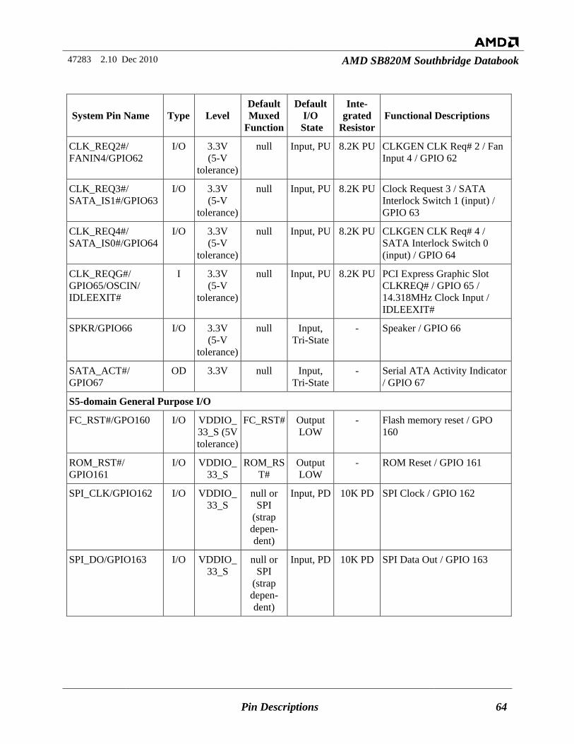
47283 2.10 Dec 2010 AMD SB820M Southbridge Databook
Pin Descriptions 64
System Pin Name Type Level Default Muxed
Function
Default I/O
State
Inte-grated
Resistor Functional Descriptions
CLK_REQ2#/ FANIN4/GPIO62
I/O 3.3V (5-V
tolerance)
null Input, PU 8.2K PU CLKGEN CLK Req# 2 / Fan Input 4 / GPIO 62
CLK_REQ3#/ SATA_IS1#/GPIO63
I/O 3.3V (5-V
tolerance)
null Input, PU 8.2K PU Clock Request 3 / SATA Interlock Switch 1 (input) / GPIO 63
CLK_REQ4#/ SATA_IS0#/GPIO64
I/O 3.3V (5-V
tolerance)
null Input, PU 8.2K PU CLKGEN CLK Req# 4 / SATA Interlock Switch 0 (input) / GPIO 64
CLK_REQG#/ GPIO65/OSCIN/ IDLEEXIT#
I 3.3V (5-V
tolerance)
null Input, PU 8.2K PU PCI Express Graphic Slot CLKREQ# / GPIO 65 / 14.318MHz Clock Input / IDLEEXIT#
SPKR/GPIO66 I/O 3.3V (5-V
tolerance)
null Input, Tri-State
- Speaker / GPIO 66
SATA_ACT#/ GPIO67
OD 3.3V null Input, Tri-State
- Serial ATA Activity Indicator / GPIO 67
S5-domain General Purpose I/O
FC_RST#/GPO160 I/O VDDIO_33_S (5V tolerance)
FC_RST# Output LOW
- Flash memory reset / GPO 160
ROM_RST#/ GPIO161
I/O VDDIO_33_S
ROM_RST#
Output LOW
- ROM Reset / GPIO 161
SPI_CLK/GPIO162 I/O VDDIO_33_S
null or SPI
(strap depen-dent)
Input, PD 10K PD SPI Clock / GPIO 162
SPI_DO/GPIO163 I/O VDDIO_33_S
null or SPI
(strap depen-dent)
Input, PD 10K PD SPI Data Out / GPIO 163
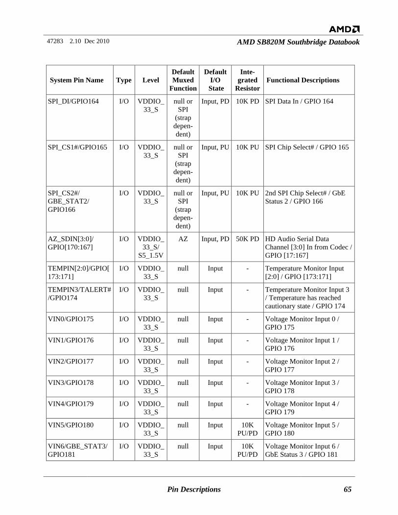
47283 2.10 Dec 2010 AMD SB820M Southbridge Databook
Pin Descriptions 65
System Pin Name Type Level Default Muxed
Function
Default I/O
State
Inte-grated
Resistor Functional Descriptions
SPI_DI/GPIO164 I/O VDDIO_33_S
null or SPI
(strap depen-dent)
Input, PD 10K PD SPI Data In / GPIO 164
SPI_CS1#/GPIO165 I/O VDDIO_33_S
null or SPI
(strap depen-dent)
Input, PU 10K PU SPI Chip Select# / GPIO 165
SPI_CS2#/ GBE_STAT2/ GPIO166
I/O VDDIO_33_S
null or SPI
(strap depen-dent)
Input, PU 10K PU 2nd SPI Chip Select# / GbE Status 2 / GPIO 166
AZ_SDIN[3:0]/ GPIO[170:167]
I/O VDDIO_33_S/
S5_1.5V
AZ Input, PD 50K PD HD Audio Serial Data Channel [3:0] In from Codec / GPIO [17:167]
TEMPIN[2:0]/GPIO[173:171]
I/O VDDIO_33_S
null Input - Temperature Monitor Input [2:0] / GPIO [173:171]
TEMPIN3/TALERT#/GPIO174
I/O VDDIO_33_S
null Input - Temperature Monitor Input 3 / Temperature has reached cautionary state / GPIO 174
VIN0/GPIO175 I/O VDDIO_33_S
null Input - Voltage Monitor Input 0 / GPIO 175
VIN1/GPIO176 I/O VDDIO_33_S
null Input - Voltage Monitor Input 1 / GPIO 176
VIN2/GPIO177 I/O VDDIO_33_S
null Input - Voltage Monitor Input 2 / GPIO 177
VIN3/GPIO178 I/O VDDIO_33_S
null Input - Voltage Monitor Input 3 / GPIO 178
VIN4/GPIO179 I/O VDDIO_33_S
null Input - Voltage Monitor Input 4 / GPIO 179
VIN5/GPIO180 I/O VDDIO_33_S
null Input 10K PU/PD
Voltage Monitor Input 5 / GPIO 180
VIN6/GBE_STAT3/GPIO181
I/O VDDIO_33_S
null Input 10K PU/PD
Voltage Monitor Input 6 / GbE Status 3 / GPIO 181
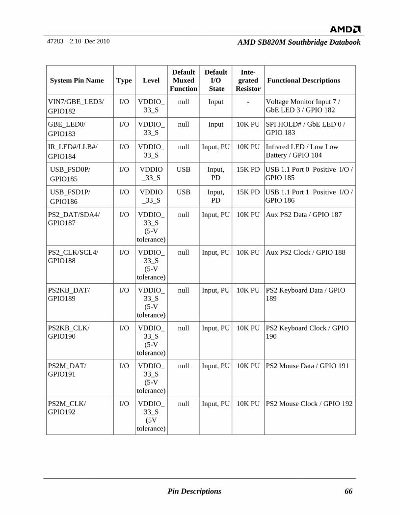
47283 2.10 Dec 2010 AMD SB820M Southbridge Databook
Pin Descriptions 66
System Pin Name Type Level Default Muxed
Function
Default I/O
State
Inte-grated
Resistor Functional Descriptions
VIN7/GBE_LED3/ GPIO182
I/O VDDIO_33_S
null Input - Voltage Monitor Input 7 / GbE LED 3 / GPIO 182
GBE_LED0/ GPIO183
I/O VDDIO_33_S
null Input 10K PU SPI HOLD# / GbE LED 0 / GPIO 183
IR_LED#/LLB#/ GPIO184
I/O VDDIO_33_S
null Input, PU 10K PU Infrared LED / Low Low Battery / GPIO 184
USB_FSD0P/ GPIO185
I/O VDDIO_33_S
USB Input, PD
15K PD USB 1.1 Port 0 Positive I/O / GPIO 185
USB_FSD1P/ GPIO186
I/O VDDIO_33_S
USB Input, PD
15K PD USB 1.1 Port 1 Positive I/O / GPIO 186
PS2_DAT/SDA4/ GPIO187
I/O VDDIO_33_S (5-V
tolerance)
null Input, PU 10K PU Aux PS2 Data / GPIO 187
PS2_CLK/SCL4/ GPIO188
I/O VDDIO_33_S (5-V
tolerance)
null Input, PU 10K PU Aux PS2 Clock / GPIO 188
PS2KB_DAT/ GPIO189
I/O VDDIO_33_S (5-V
tolerance)
null Input, PU 10K PU PS2 Keyboard Data / GPIO 189
PS2KB_CLK/ GPIO190
I/O VDDIO_33_S (5-V
tolerance)
null Input, PU 10K PU PS2 Keyboard Clock / GPIO 190
PS2M_DAT/ GPIO191
I/O VDDIO_33_S (5-V
tolerance)
null Input, PU 10K PU PS2 Mouse Data / GPIO 191
PS2M_CLK/ GPIO192
I/O VDDIO_33_S (5V
tolerance)
null Input, PU 10K PU PS2 Mouse Clock / GPIO 192
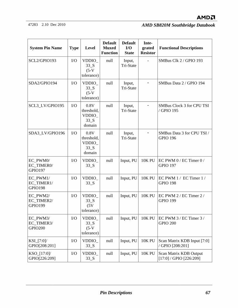
47283 2.10 Dec 2010 AMD SB820M Southbridge Databook
Pin Descriptions 67
System Pin Name Type Level Default Muxed
Function
Default I/O
State
Inte-grated
Resistor Functional Descriptions
SCL2/GPIO193 I/O VDDIO_33_S (5-V
tolerance)
null Input, Tri-State
- SMBus Clk 2 / GPIO 193
SDA2/GPIO194 I/O VDDIO_33_S (5-V
tolerance)
null Input, Tri-State
- SMBus Data 2 / GPIO 194
SCL3_LV/GPIO195 I/O 0.8V threshold, VDDIO_
33_S domain
null Input, Tri-State
- SMBus Clock 3 for CPU TSI / GPIO 195
SDA3_LV/GPIO196 I/O 0.8V threshold, VDDIO_
33_S domain
null Input, Tri-State
- SMBus Data 3 for CPU TSI / GPIO 196
EC_PWM0/ EC_TIMER0/ GPIO197
I/O VDDIO_33_S
null Input, PU 10K PU EC PWM 0 / EC Timer 0 / GPIO 197
EC_PWM1/ EC_TIMER1/ GPIO198
I/O VDDIO_33_S
null Input, PU 10K PU EC PWM 1 / EC Timer 1 / GPIO 198
EC_PWM2/ EC_TIMER2/ GPIO199
I/O VDDIO_33_S (5V
tolerance)
null Input, PU 10K PU EC PWM 2 / EC Timer 2 / GPIO 199
EC_PWM3/ EC_TIMER3/ GPIO200
I/O VDDIO_33_S (5-V
tolerance)
null Input, PU 10K PU EC PWM 3 / EC Timer 3 / GPIO 200
KSI_[7:0]/ GPIO[208:201]
I/O VDDIO_33_S
null Input, PU 10K PU Scan Matrix KDB Input [7:0] / GPIO [208:201]
KSO_[17:0]/ GPIO[226:209]
I/O VDDIO_33_S
null Input, PU 10K PU Scan Matrix KDB Output [17:0] / GPIO [226:209]
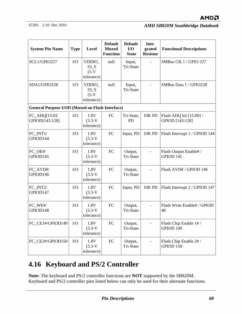
47283 2.10 Dec 2010 AMD SB820M Southbridge Databook
Pin Descriptions 68
System Pin Name Type Level Default Muxed
Function
Default I/O
State
Inte-grated
Resistor Functional Descriptions
SCL1/GPIO227 I/O VDDIO_33_S (5-V
tolerance)
null Input, Tri-State
- SMBus Clk 1 / GPIO 227
SDA1/GPIO228 I/O VDDIO_33_S (5-V
tolerance)
null Input, Tri-State
- SMBus Data 1 / GPIO228
General Purpose I/OD (Muxed on Flash Interface)
FC_ADQ[15:0]/ GPIOD[143:128]
I/O 1.8V (3.3-V
tolerance)
FC Tri-State, PD
10K PD Flash ADQ bit [15:00] / GPIOD [143:128]
FC_INT1/ GPIOD144
I/O 1.8V (3.3-V
tolerance)
FC Input, PD 10K PD Flash Interrupt 1 / GPIOD 144
FC_OE#/ GPIOD145
I/O 1.8V (3.3-V
tolerance)
FC Output, Tri-State
- Flash Output Enable# / GPIOD 145
FC_AVD#/ GPIOD146
I/O 1.8V (3.3-V
tolerance)
FC Output, Tri-State
- Flash AVD# / GPIOD 146
FC_INT2/ GPIOD147
I/O 1.8V (3.3-V
tolerance)
FC Input, PD 10K PD Flash Interrupt 2 / GPIOD 147
FC_WE#/ GPIOD148
I/O 1.8V (3.3-V
tolerance)
FC Output, Tri-State
- Flash Write Enable# / GPIOD 48
FC_CE1#/GPIOD149 I/O 1.8V (3.3-V
tolerance)
FC Output, Tri-State
- Flash Chip Enable 1# / GPIOD 149
FC_CE2#/GPIOD150 I/O 1.8V (3.3-V
tolerance)
FC Output, Tri-State
- Flash Chip Enable 2# / GPIOD 150
4.16 Keyboard and PS/2 Controller Note: The keyboard and PS/2 controller functions are NOT supported by the SB820M. Keyboard and PS/2 controller pins listed below can only be used for their alternate functions.
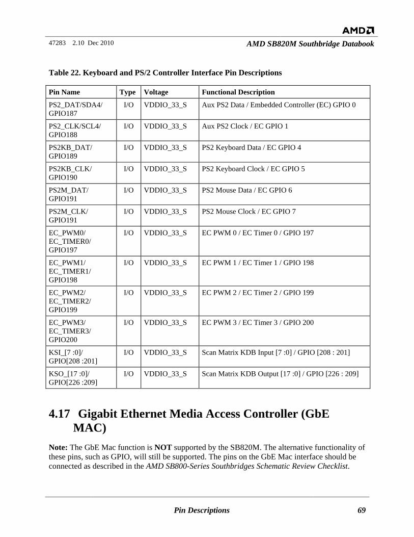
47283 2.10 Dec 2010 AMD SB820M Southbridge Databook
Pin Descriptions 69
Table 22. Keyboard and PS/2 Controller Interface Pin Descriptions
Pin Name Type Voltage Functional Description
PS2_DAT/SDA4/ GPIO187
I/O VDDIO_33_S Aux PS2 Data / Embedded Controller (EC) GPIO 0
PS2_CLK/SCL4/ GPIO188
I/O VDDIO_33_S Aux PS2 Clock / EC GPIO 1
PS2KB_DAT/ GPIO189
I/O VDDIO_33_S PS2 Keyboard Data / EC GPIO 4
PS2KB_CLK/ GPIO190
I/O VDDIO_33_S PS2 Keyboard Clock / EC GPIO 5
PS2M_DAT/ GPIO191
I/O VDDIO_33_S PS2 Mouse Data / EC GPIO 6
PS2M_CLK/ GPIO191
I/O VDDIO_33_S PS2 Mouse Clock / EC GPIO 7
EC_PWM0/ EC_TIMER0/ GPIO197
I/O VDDIO_33_S EC PWM 0 / EC Timer 0 / GPIO 197
EC_PWM1/ EC_TIMER1/ GPIO198
I/O VDDIO_33_S EC PWM 1 / EC Timer 1 / GPIO 198
EC_PWM2/ EC_TIMER2/ GPIO199
I/O VDDIO_33_S EC PWM 2 / EC Timer 2 / GPIO 199
EC_PWM3/ EC_TIMER3/ GPIO200
I/O VDDIO_33_S EC PWM 3 / EC Timer 3 / GPIO 200
KSI_[7 :0]/ GPIO[208 :201]
I/O VDDIO_33_S Scan Matrix KDB Input [7 :0] / GPIO [208 : 201]
KSO_[17 :0]/ GPIO[226 :209]
I/O VDDIO_33_S Scan Matrix KDB Output [17 :0] / GPIO [226 : 209]
4.17 Gigabit Ethernet Media Access Controller (GbE MAC)
Note: The GbE Mac function is NOT supported by the SB820M. The alternative functionality of these pins, such as GPIO, will still be supported. The pins on the GbE Mac interface should be connected as described in the AMD SB800-Series Southbridges Schematic Review Checklist.
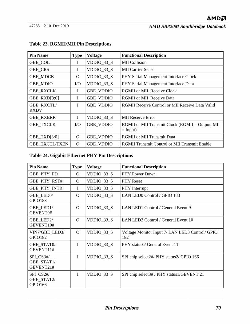
47283 2.10 Dec 2010 AMD SB820M Southbridge Databook
Pin Descriptions 70
Table 23. RGMII/MII Pin Descriptions
Pin Name Type Voltage Functional Description GBE_COL I VDDIO_33_S MII Collision GBE_CRS I VDDIO_33_S MII Carrier Sense GBE_MDCK O VDDIO_33_S PHY Serial Management Interface Clock GBE_MDIO I/O VDDIO_33_S PHY Serial Management Interface Data GBE_RXCLK I GBE_VDDIO RGMII or MII Receive Clock GBE_RXD[3:0] I GBE_VDDIO RGMII or MII Receive Data GBE_RXCTL/ RXDV
I GBE_VDDIO RGMII Receive Control or MII Receive Data Valid
GBE_RXERR I VDDIO_33_S MII Receive Error GBE_TXCLK I/O GBE_VDDIO RGMII or MII Transmit Clock (RGMII = Output, MII
= Input) GBE_TXD[3:0] O GBE_VDDIO RGMII or MII Transmit Data GBE_TXCTL/TXEN O GBE_VDDIO RGMII Transmit Control or MII Transmit Enable
Table 24. Gigabit Ethernet PHY Pin Descriptions
Pin Name Type Voltage Functional Description GBE_PHY_PD O VDDIO_33_S PHY Power Down GBE_PHY_RST# O VDDIO_33_S PHY Reset GBE_PHY_INTR I VDDIO_33_S PHY Interrupt GBE_LED0/ GPIO183
O VDDIO_33_S LAN LED0 Control / GPIO 183
GBE_LED1/ GEVENT9#
O VDDIO_33_S LAN LED1 Control / General Event 9
GBE_LED2/ GEVENT10#
O VDDIO_33_S LAN LED2 Control / General Event 10
VIN7/GBE_LED3/ GPIO182
O VDDIO_33_S Voltage Monitor Input 7/ LAN LED3 Control/ GPIO 182
GBE_STAT0/ GEVENT11#
I VDDIO_33_S PHY status0/ General Event 11
SPI_CS3#/ GBE_STAT1/ GEVENT21#
I VDDIO_33_S SPI chip select2#/ PHY status2/ GPIO 166
SPI_CS2#/ GBE_STAT2/ GPIO166
I VDDIO_33_S SPI chip select3# / PHY status1/GEVENT 21
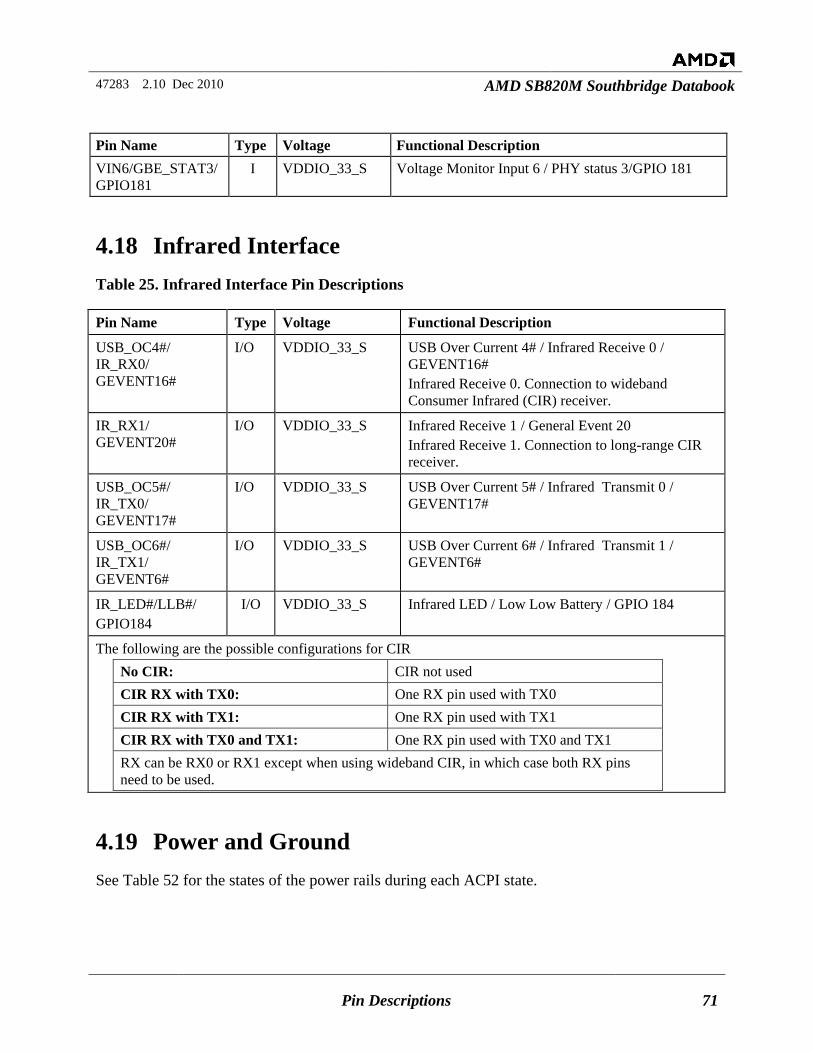
47283 2.10 Dec 2010 AMD SB820M Southbridge Databook
Pin Descriptions 71
Pin Name Type Voltage Functional Description VIN6/GBE_STAT3/ GPIO181
I VDDIO_33_S Voltage Monitor Input 6 / PHY status 3/GPIO 181
4.18 Infrared Interface Table 25. Infrared Interface Pin Descriptions
Pin Name Type Voltage Functional Description
USB_OC4#/ IR_RX0/ GEVENT16#
I/O VDDIO_33_S USB Over Current 4# / Infrared Receive 0 / GEVENT16# Infrared Receive 0. Connection to wideband Consumer Infrared (CIR) receiver.
IR_RX1/ GEVENT20#
I/O VDDIO_33_S Infrared Receive 1 / General Event 20 Infrared Receive 1. Connection to long-range CIR receiver.
USB_OC5#/ IR_TX0/ GEVENT17#
I/O VDDIO_33_S USB Over Current 5# / Infrared Transmit 0 / GEVENT17#
USB_OC6#/ IR_TX1/ GEVENT6#
I/O VDDIO_33_S USB Over Current 6# / Infrared Transmit 1 / GEVENT6#
IR_LED#/LLB#/ GPIO184
I/O VDDIO_33_S Infrared LED / Low Low Battery / GPIO 184
The following are the possible configurations for CIR No CIR: CIR not used CIR RX with TX0: One RX pin used with TX0 CIR RX with TX1: One RX pin used with TX1 CIR RX with TX0 and TX1: One RX pin used with TX0 and TX1 RX can be RX0 or RX1 except when using wideband CIR, in which case both RX pins need to be used.
4.19 Power and Ground See Table 52 for the states of the power rails during each ACPI state.
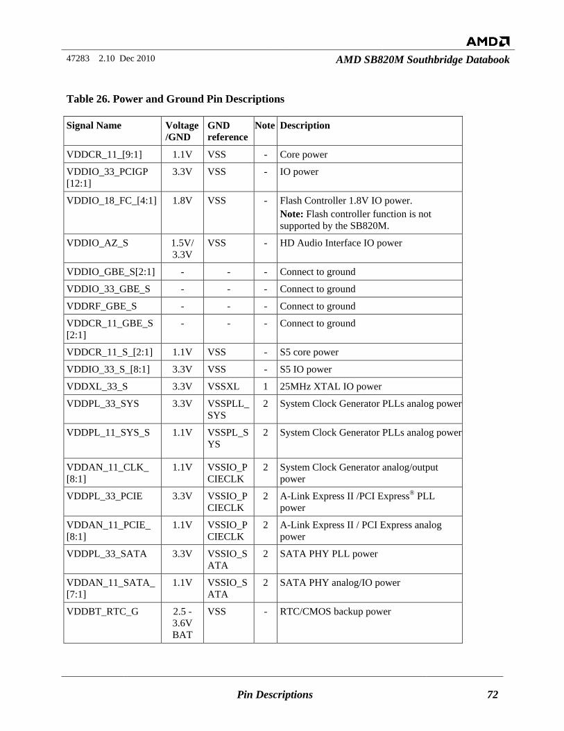
47283 2.10 Dec 2010 AMD SB820M Southbridge Databook
Pin Descriptions 72
Table 26. Power and Ground Pin Descriptions
Signal Name Voltage/GND
GND reference
Note Description
VDDCR_11_[9:1] 1.1V VSS - Core power
VDDIO_33_PCIGP [12:1]
3.3V VSS - IO power
VDDIO_18_FC_[4:1] 1.8V VSS - Flash Controller 1.8V IO power. Note: Flash controller function is not supported by the SB820M.
VDDIO_AZ_S 1.5V/ 3.3V
VSS - HD Audio Interface IO power
VDDIO_GBE_S[2:1] - - - Connect to ground
VDDIO_33_GBE_S - - - Connect to ground
VDDRF_GBE_S - - - Connect to ground
VDDCR_11_GBE_S [2:1]
- - - Connect to ground
VDDCR_11_S_[2:1] 1.1V VSS - S5 core power
VDDIO_33_S_[8:1] 3.3V VSS - S5 IO power
VDDXL_33_S 3.3V VSSXL 1 25MHz XTAL IO power
VDDPL_33_SYS 3.3V VSSPLL_SYS
2 System Clock Generator PLLs analog power
VDDPL_11_SYS_S 1.1V VSSPL_SYS
2 System Clock Generator PLLs analog power
VDDAN_11_CLK_ [8:1]
1.1V VSSIO_PCIECLK
2 System Clock Generator analog/output power
VDDPL_33_PCIE 3.3V VSSIO_PCIECLK
2 A-Link Express II /PCI Express® PLL power
VDDAN_11_PCIE_ [8:1]
1.1V VSSIO_PCIECLK
2 A-Link Express II / PCI Express analog power
VDDPL_33_SATA 3.3V VSSIO_SATA
2 SATA PHY PLL power
VDDAN_11_SATA_ [7:1]
1.1V VSSIO_SATA
2 SATA PHY analog/IO power
VDDBT_RTC_G 2.5 - 3.6V BAT
VSS - RTC/CMOS backup power
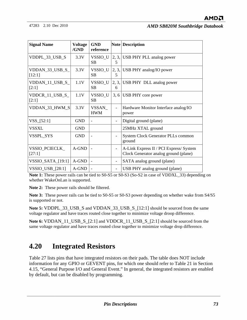
47283 2.10 Dec 2010 AMD SB820M Southbridge Databook
Pin Descriptions 73
Signal Name Voltage/GND
GND reference
Note Description
VDDPL_33_USB_S 3.3V VSSIO_USB
2, 3, 5
USB PHY PLL analog power
VDDAN_33_USB_S_[12:1]
3.3V VSSIO_USB
2, 3, 5
USB PHY analog/IO power
VDDAN_11_USB_S_[2:1]
1.1V VSSIO_USB
2, 3, 6
USB PHY DLL analog power
VDDCR_11_USB_S_[2:1]
1.1V VSSIO_USB
3, 6 USB PHY core power
VDDAN_33_HWM_S 3.3V VSSAN_HWM
- Hardware Monitor Interface analog/IO power
VSS_[52:1] GND - - Digital ground (plane)
VSSXL GND 25MHz XTAL ground
VSSPL_SYS GND - - System Clock Generator PLLs common ground
VSSIO_PCIECLK_ [27:1]
A-GND - - A-Link Express II / PCI Express/ System Clock Generator analog ground (plane)
VSSIO_SATA_[19:1] A-GND - - SATA analog ground (plane)
VSSIO_USB_[28:1] A-GND - - USB PHY analog ground (plane) Note 1: These power rails can be tied to S0-S5 or S0-S3 (So-S2 in case of VDDXL_33) depending on whether WakeOnLan is supported.
Note 2: These power rails should be filtered.
Note 3: These power rails can be tied to S0-S5 or S0-S3 power depending on whether wake from S4/S5 is supported or not.
Note 5: VDDPL_33_USB_S and VDDAN_33_USB_S_[12:1] should be sourced from the same voltage regulator and have traces routed close together to minimize voltage droop difference.
Note 6: VDDAN_11_USB_S_[2:1] and VDDCR_11_USB_S_[2:1] should be sourced from the same voltage regulator and have traces routed close together to minimize voltage drop difference.
4.20 Integrated Resistors Table 27 lists pins that have integrated resistors on their pads. The table does NOT include information for any GPIO or GEVENT pins, for which one should refer to Table 21 in Section 4.15, “General Purpose I/O and General Event.” In general, the integrated resistors are enabled by default, but can be disabled by programming.
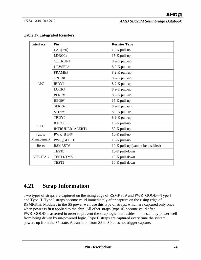
47283 2.10 Dec 2010 AMD SB820M Southbridge Databook
Pin Descriptions 74
Table 27. Integrated Resistors
Interface Pin Resistor Type
LPC
LAD[3:0] 15-K pull-up LDRQ0# 15-K pull-up CLKRUN# 8.2-K pull-up DEVSEL# 8.2-K pull-up FRAME# 8.2-K pull-up GNT3# 8.2-K pull-up IRDY# 8.2-K pull-up LOCK# 8.2-K pull-up PERR# 8.2-K pull-up REQ0# 15-K pull-up SERR# 8.2-K pull-up STOP# 8.2-K pull-up TRDY# 8.2-K pull-up
RTC RTCCLK 10-K pull-up INTRUDER_ALERT# 50-K pull-up
Power Management
PWR_BTN# 10-K pull-up PWR_GOOD 10-K pull-up
Reset RSMRST# 10-K pull-up (cannot be disabled)
ATE/JTAG TEST0 10-K pull-down TEST1/TMS 10-K pull-down TEST2 10-K pull-down
4.21 Strap Information Two types of straps are captured on the rising edge of RSMRST# and PWR_GOOD—Type I and Type II. Type I straps become valid immediately after capture on the rising edge of RSMRST#. Modules in the S5 power well use this type of straps, which are captured only once when power is first applied to the chip. All other straps (type II) become valid after PWR_GOOD is asserted in order to prevent the strap logic that resides in the standby power well from being driven by un-powered logic. Type II straps are captured every time the system powers up from the S5 state. A transition from S3 to S0 does not trigger capture.
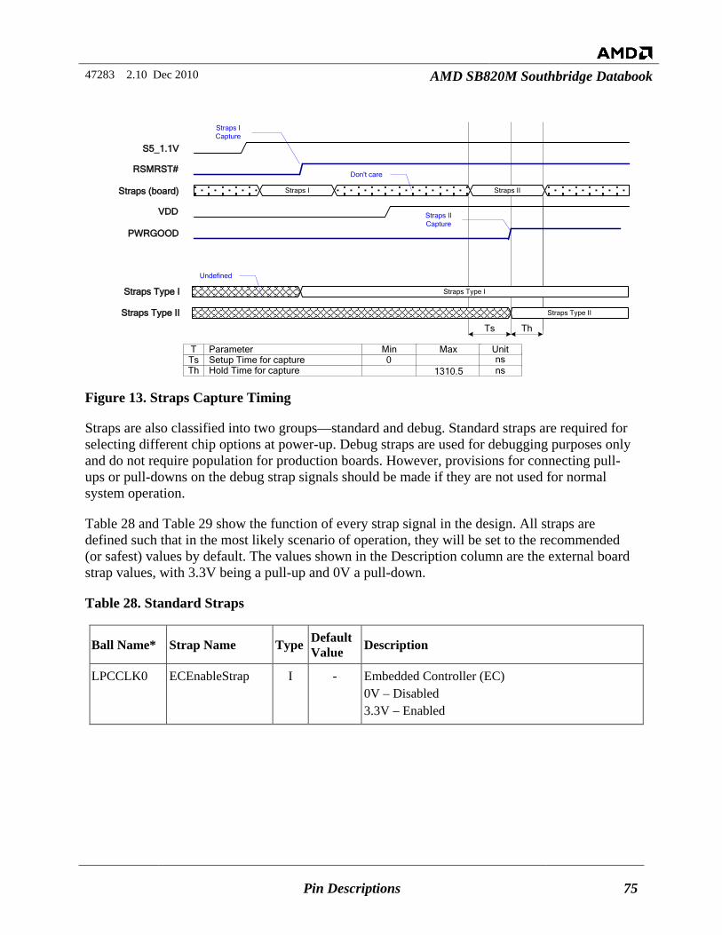
47283 2.10 Dec 2010 AMD SB820M Southbridge Databook
Pin Descriptions 75
S5_1.1V
Straps (board)
PWRGOOD
Setup Time for capture 0Parameter Min Max
Hold Time for capture 1310.5
RSMRST#
VDD
TTsTh
nsUnit
ns
Ts Th
Straps Type I
Straps ICapture
Straps Type II
Straps I
Straps Type I
Straps Type II
Undefined
Straps IICapture
Straps II
Don't care
Figure 13. Straps Capture Timing
Straps are also classified into two groups—standard and debug. Standard straps are required for selecting different chip options at power-up. Debug straps are used for debugging purposes only and do not require population for production boards. However, provisions for connecting pull-ups or pull-downs on the debug strap signals should be made if they are not used for normal system operation.
Table 28 and Table 29 show the function of every strap signal in the design. All straps are defined such that in the most likely scenario of operation, they will be set to the recommended (or safest) values by default. The values shown in the Description column are the external board strap values, with 3.3V being a pull-up and 0V a pull-down.
Table 28. Standard Straps
Ball Name* Strap Name Type Default Value Description
LPCCLK0 ECEnableStrap I - Embedded Controller (EC) 0V – Disabled 3.3V – Enabled
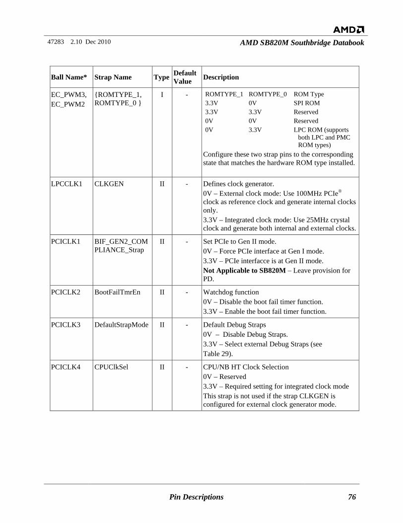
47283 2.10 Dec 2010 AMD SB820M Southbridge Databook
Pin Descriptions 76
Ball Name* Strap Name Type Default Value Description
EC_PWM3, EC_PWM2
ROMTYPE_1, ROMTYPE_0
I - ROMTYPE_1 ROMTYPE_0 ROM Type 3.3V 0V SPI ROM 3.3V 3.3V Reserved 0V 0V Reserved 0V 3.3V LPC ROM (supports both LPC and PMC ROM types)
Configure these two strap pins to the corresponding state that matches the hardware ROM type installed.
LPCCLK1 CLKGEN II - Defines clock generator. 0V – External clock mode: Use 100MHz PCIe® clock as reference clock and generate internal clocks only. 3.3V – Integrated clock mode: Use 25MHz crystal clock and generate both internal and external clocks.
PCICLK1
BIF_GEN2_COMPLIANCE_Strap
II - Set PCIe to Gen II mode. 0V – Force PCIe interface at Gen I mode. 3.3V – PCIe interfacce is at Gen II mode. Not Applicable to SB820M – Leave provision for PD.
PCICLK2 BootFailTmrEn II - Watchdog function 0V – Disable the boot fail timer function. 3.3V – Enable the boot fail timer function.
PCICLK3 DefaultStrapMode II - Default Debug Straps 0V – Disable Debug Straps. 3.3V – Select external Debug Straps (see Table 29).
PCICLK4 CPUClkSel II - CPU/NB HT Clock Selection 0V – Reserved 3.3V – Required setting for integrated clock mode This strap is not used if the strap CLKGEN is configured for external clock generator mode.
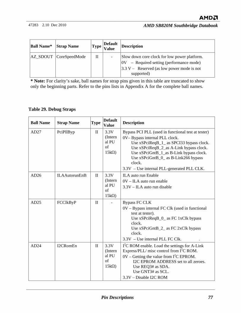
47283 2.10 Dec 2010 AMD SB820M Southbridge Databook
Pin Descriptions 77
Ball Name* Strap Name Type Default Value Description
AZ_SDOUT CoreSpeedMode II - Slow down core clock for low power platform. 0V – Required setting (performance mode) 3.3 V – Reserved (as low power mode is not
supported)
* Note: For clarity’s sake, ball names for strap pins given in this table are truncated to show only the beginning parts. Refer to the pins lists in Appendix A for the complete ball names.
Table 29. Debug Straps
Ball Name Strap Name Type Default Value Description
AD27 PciPllByp II 3.3V (Internal PU of 15kΩ)
Bypass PCI PLL (used in functional test at tester) 0V– Bypass internal PLL clock.
Use xSPciReqB_1_ as SPCI33 bypass clock. Use xSPciReqB_2_as A-Link bypass clock. Use xSPciGntB_1_as B-Link bypass clock. Use xSPciGntB_0_ as B-Link266 bypass clock.
3.3V – Use internal PLL-generated PLL CLK. AD26 ILAAutorunEnB II 3.3V
(Internal PU of 15kΩ)
ILA auto run Enable 0V – ILA auto run enable 3.3V – ILA auto run disable
AD25 FCClkByP II - Bypass FC CLK 0V – Bypass internal FC Clk (used in functional
test at tester). Use xSPciReqB_0_ as FC 1xClk bypass clock. Use xSPciGntB_2_ as FC 2xClk bypass clock.
3.3V – Use internal PLL FC Clk. . AD24 I2CRomEn II 3.3V
(Internal PU of 15kΩ)
I2C ROM enable. Load the settings for A-Link Express/PLL/ misc control from I2C ROM. 0V – Getting the value from I2C EPROM.
I2C EPROM ADDRESS set to all zeroes. Use REQ3# as SDA. Use GNT3# as SCL.
3.3V – Disable I2C ROM
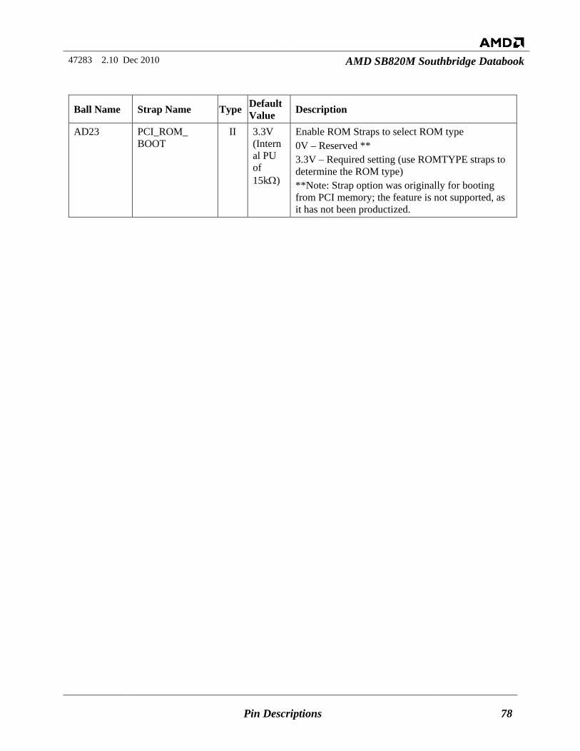
47283 2.10 Dec 2010 AMD SB820M Southbridge Databook
Pin Descriptions 78
Ball Name Strap Name Type Default Value Description
AD23 PCI_ROM_ BOOT
II 3.3V (Internal PU of 15kΩ)
Enable ROM Straps to select ROM type 0V – Reserved ** 3.3V – Required setting (use ROMTYPE straps to determine the ROM type) **Note: Strap option was originally for booting from PCI memory; the feature is not supported, as it has not been productized.
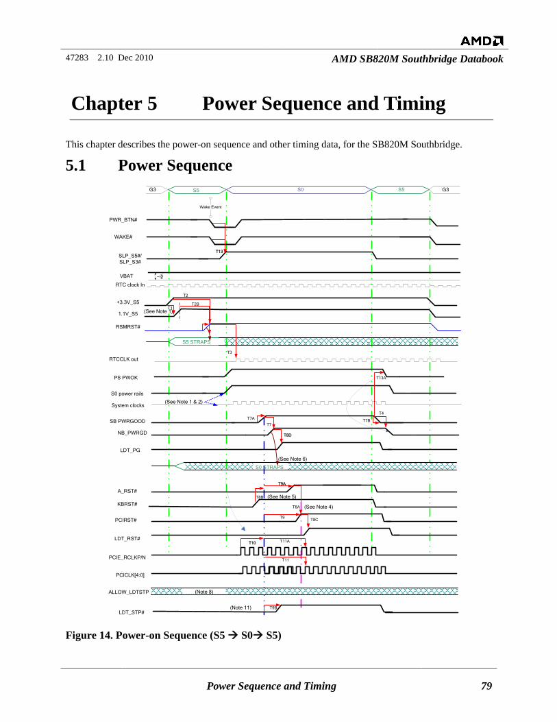
47283 2.10 Dec 2010 AMD SB820M Southbridge Databook
Power Sequence and Timing 79
Chapter 5 Power Sequence and Timing
This chapter describes the power-on sequence and other timing data, for the SB820M Southbridge.
5.1 Power Sequence
T1T2B
S5 S5 G3G3 S0
S5 STRAPS
VBATVBAT
RTC clock In
+3.3V_S5
1.1V_S5
RSMRST#
S0 power rails
SB PWRGOOD
A_RST#
S0 STRAPS
KBRST#
T8B
PCIRST#
PCIE_RCLKP/N
T2
PCICLK[4:0]
(See Note 1)
NB_PWRGD
T7
T7A
LDT_PG
(See Note 5)
T11
T8A
T9
T9A
LDT_STP#
(Note 8)
Wake Event
SLP_S5#/SLP_S3#
T13
T8D
LDT_RST#
ALLOW_LDTSTP
WAKE#
PWR_BTN#
PS PWOK T13A
T7B
(See Note 4)
T8C
(See Note 6)
RTCCLK outT3
T10
System clocks(See Note 1 & 2)
T4
T9B(Note 11)
T11A
Figure 14. Power-on Sequence (S5 S0 S5)
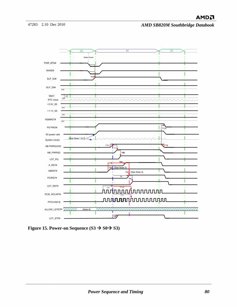
47283 2.10 Dec 2010 AMD SB820M Southbridge Databook
Power Sequence and Timing 80
S3 S3S0
VBATVBAT
RTC clock
+3.3V_S5
+1.1V_S5
RSMRST#
S0 power rails
SB PWRGOOD
A_RST#
KBRST#
T8B
PCIRST#
T10
PCIE_RCLKP/N
PCICLK[4:0]
NB_PWRGD
T7
T7A
LDT_PG
(See Note 5)
T11
T8A
T9
T9A
LDT_STP#
(Note 8)
Wake Event
SLP_S3#T13
T8D
LDT_RST#
ALLOW_LDTSTP
WAKE#
PWR_BTN#
PS PWOK T13A
T7B
(See Note 4)
SLP_S5#GND
GND
GND
GND
GND
T8C
System clocks(See Note 1 & 2)
T9B
T11A
Figure 15. Power-on Sequence (S3 S0 S3)
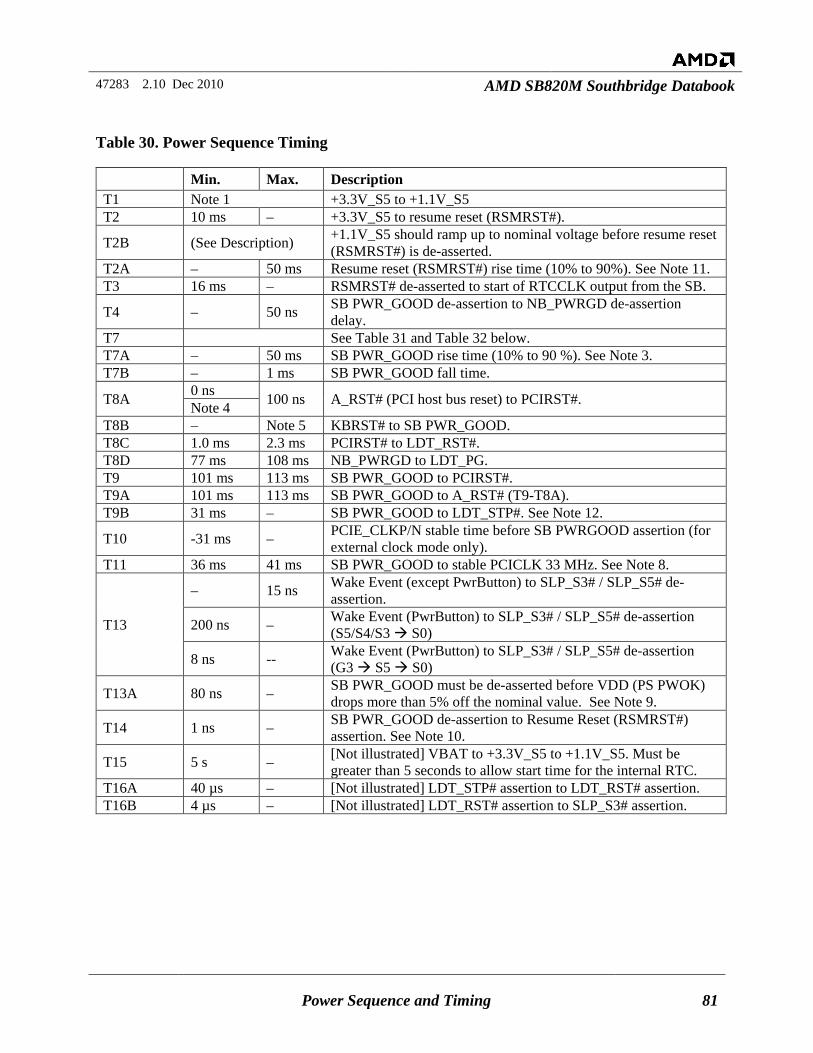
47283 2.10 Dec 2010 AMD SB820M Southbridge Databook
Power Sequence and Timing 81
Table 30. Power Sequence Timing
Min. Max. Description T1 Note 1 +3.3V_S5 to +1.1V_S5 T2 10 ms – +3.3V_S5 to resume reset (RSMRST#).
T2B (See Description) +1.1V_S5 should ramp up to nominal voltage before resume reset (RSMRST#) is de-asserted.
T2A – 50 ms Resume reset (RSMRST#) rise time (10% to 90%). See Note 11. T3 16 ms – RSMRST# de-asserted to start of RTCCLK output from the SB.
T4 – 50 ns SB PWR_GOOD de-assertion to NB_PWRGD de-assertion delay.
T7 See Table 31 and Table 32 below. T7A – 50 ms SB PWR_GOOD rise time (10% to 90 %). See Note 3. T7B – 1 ms SB PWR_GOOD fall time.
T8A 0 ns 100 ns A_RST# (PCI host bus reset) to PCIRST#. Note 4 T8B – Note 5 KBRST# to SB PWR_GOOD. T8C 1.0 ms 2.3 ms PCIRST# to LDT_RST#. T8D 77 ms 108 ms NB_PWRGD to LDT_PG. T9 101 ms 113 ms SB PWR_GOOD to PCIRST#. T9A 101 ms 113 ms SB PWR_GOOD to A_RST# (T9-T8A). T9B 31 ms – SB PWR_GOOD to LDT_STP#. See Note 12.
T10 -31 ms – PCIE_CLKP/N stable time before SB PWRGOOD assertion (for external clock mode only).
T11 36 ms 41 ms SB PWR_GOOD to stable PCICLK 33 MHz. See Note 8.
T13
– 15 ns Wake Event (except PwrButton) to SLP_S3# / SLP_S5# de-assertion.
200 ns – Wake Event (PwrButton) to SLP_S3# / SLP_S5# de-assertion (S5/S4/S3 S0)
8 ns -- Wake Event (PwrButton) to SLP_S3# / SLP_S5# de-assertion (G3 S5 S0)
T13A 80 ns – SB PWR_GOOD must be de-asserted before VDD (PS PWOK) drops more than 5% off the nominal value. See Note 9.
T14 1 ns – SB PWR_GOOD de-assertion to Resume Reset (RSMRST#) assertion. See Note 10.
T15 5 s – [Not illustrated] VBAT to +3.3V_S5 to +1.1V_S5. Must be greater than 5 seconds to allow start time for the internal RTC.
T16A 40 µs – [Not illustrated] LDT_STP# assertion to LDT_RST# assertion. T16B 4 µs – [Not illustrated] LDT_RST# assertion to SLP_S3# assertion.
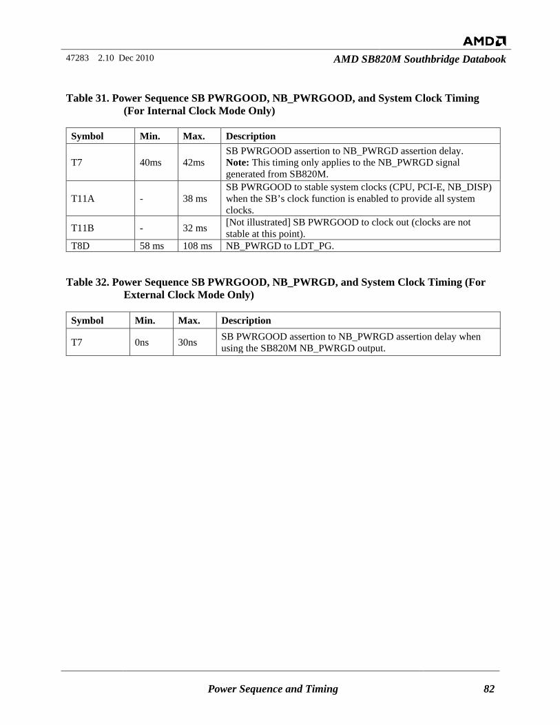
47283 2.10 Dec 2010 AMD SB820M Southbridge Databook
Power Sequence and Timing 82
Table 31. Power Sequence SB PWRGOOD, NB_PWRGOOD, and System Clock Timing (For Internal Clock Mode Only)
Symbol Min. Max. Description
T7 40ms 42ms SB PWRGOOD assertion to NB_PWRGD assertion delay. Note: This timing only applies to the NB_PWRGD signal generated from SB820M.
T11A - 38 ms SB PWRGOOD to stable system clocks (CPU, PCI-E, NB_DISP) when the SB’s clock function is enabled to provide all system clocks.
T11B - 32 ms [Not illustrated] SB PWRGOOD to clock out (clocks are not stable at this point).
T8D 58 ms 108 ms NB_PWRGD to LDT_PG.
Table 32. Power Sequence SB PWRGOOD, NB_PWRGD, and System Clock Timing (For External Clock Mode Only)
Symbol Min. Max. Description
T7 0ns 30ns SB PWRGOOD assertion to NB_PWRGD assertion delay when using the SB820M NB_PWRGD output.
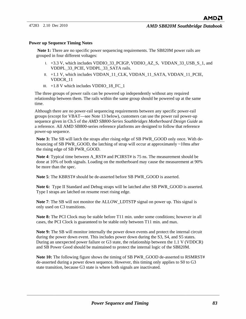
47283 2.10 Dec 2010 AMD SB820M Southbridge Databook
Power Sequence and Timing 83
Power up Sequence Timing Notes
Note 1: There are no specific power sequencing requirements. The SB820M power rails are grouped in four different voltages:
I. +3.3 V, which includes VDDIO_33_PCIGP, VDDIO_AZ_S, VDDAN_33_USB_S_1, and VDDPL_33_PCIE, VDDPL_33_SATA rails.
II. +1.1 V, which includes VDDAN_11_CLK, VDDAN_11_SATA, VDDAN_11_PCIE, VDDCR_11
III. +1.8 V which includes VDDIO_18_FC_1
The three groups of power rails can be powered up independently without any required relationship between them. The rails within the same group should be powered up at the same time.
Although there are no power-rail sequencing requirements between any specific power-rail groups (except for VBAT—see Note 13 below), customers can use the power rail power-up sequence given in Ch.5 of the AMD SB800-Series Southbridges Motherboard Design Guide as a reference. All AMD SB800-series reference platforms are designed to follow that reference power-up sequence.
Note 3: The SB will latch the straps after rising edge of SB PWR_GOOD only once. With de-bouncing of SB PWR_GOOD, the latching of strap will occur at approximately ~10ms after the rising edge of SB PWR_GOOD.
Note 4: Typical time between A_RST# and PCIRST# is 75 ns. The measurement should be done at 10% of both signals. Loading on the motherboard may cause the measurement at 90% be more than the spec.
Note 5: The KBRST# should be de-asserted before SB PWR_GOOD is asserted.
Note 6: Type II Standard and Debug straps will be latched after SB PWR_GOOD is asserted. Type I straps are latched on resume reset rising edge.
Note 7: The SB will not monitor the ALLOW_LDTSTP signal on power up. This signal is only used on C3 transitions.
Note 8: The PCI Clock may be stable before T11 min. under some conditions; however in all cases, the PCI Clock is guaranteed to be stable only between T11 min. and max.
Note 9: The SB will monitor internally the power down events and protect the internal circuit during the power down event. This includes power down during the S3, S4, and S5 states. During an unexpected power failure or G3 state, the relationship between the 1.1 V (VDDCR) and SB Power Good should be maintained to protect the internal logic of the SB820M.
Note 10: The following figure shows the timing of SB PWR_GOOD de-asserted to RSMRST# de-asserted during a power down sequence. However, this timing only applies to S0 to G3 state transition, because G3 state is where both signals are inactivated.
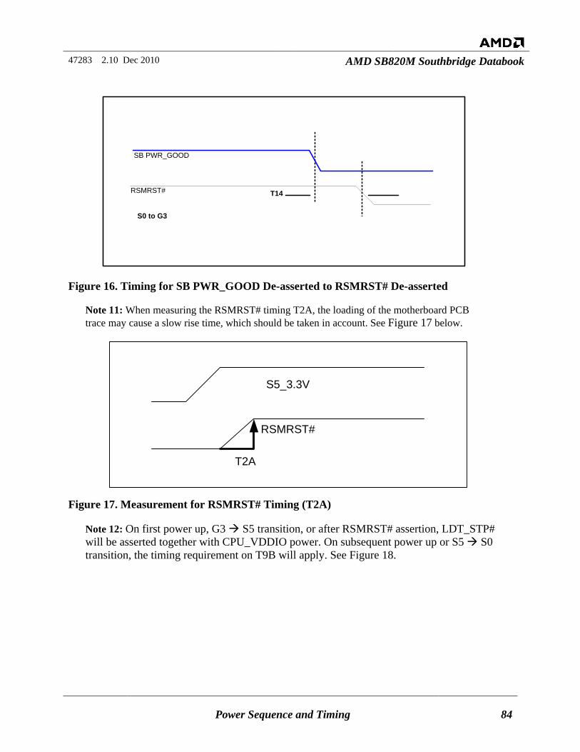
47283 2.10 Dec 2010 AMD SB820M Southbridge Databook
Power Sequence and Timing 84
SB PWR_GOOD
T14RSMRST#
S0 to G3
Figure 16. Timing for SB PWR_GOOD De-asserted to RSMRST# De-asserted
Note 11: When measuring the RSMRST# timing T2A, the loading of the motherboard PCB trace may cause a slow rise time, which should be taken in account. See Figure 17 below.
RSMRST#
S5_3.3V
T2A
Figure 17. Measurement for RSMRST# Timing (T2A)
Note 12: On first power up, G3 S5 transition, or after RSMRST# assertion, LDT_STP# will be asserted together with CPU_VDDIO power. On subsequent power up or S5 S0 transition, the timing requirement on T9B will apply. See Figure 18.
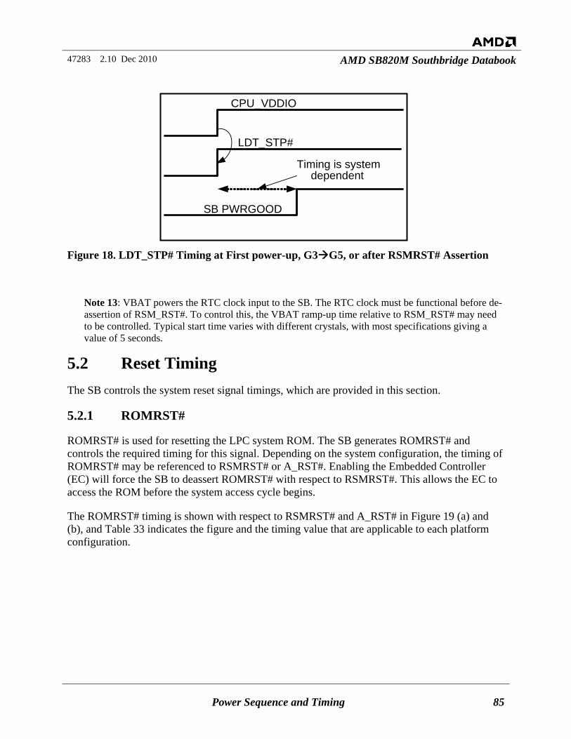
47283 2.10 Dec 2010 AMD SB820M Southbridge Databook
Power Sequence and Timing 85
Figure 18. LDT_STP# Timing at First power-up, G3G5, or after RSMRST# Assertion
Note 13: VBAT powers the RTC clock input to the SB. The RTC clock must be functional before de-assertion of RSM_RST#. To control this, the VBAT ramp-up time relative to RSM_RST# may need to be controlled. Typical start time varies with different crystals, with most specifications giving a value of 5 seconds.
5.2 Reset Timing The SB controls the system reset signal timings, which are provided in this section.
5.2.1 ROMRST#
ROMRST# is used for resetting the LPC system ROM. The SB generates ROMRST# and controls the required timing for this signal. Depending on the system configuration, the timing of ROMRST# may be referenced to RSMRST# or A_RST#. Enabling the Embedded Controller (EC) will force the SB to deassert ROMRST# with respect to RSMRST#. This allows the EC to access the ROM before the system access cycle begins.
The ROMRST# timing is shown with respect to RSMRST# and A_RST# in Figure 19 (a) and (b), and Table 33 indicates the figure and the timing value that are applicable to each platform configuration.
CPU _ VDDIO
LDT _ STP #
SB PWRGOOD
Timing is system dependent
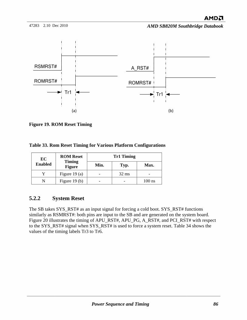
47283 2.10 Dec 2010 AMD SB820M Southbridge Databook
Power Sequence and Timing 86
Tr1
RSMRST#
ROMRST#
A_RST#
ROMRST#
Tr1
(a) (b)
Figure 19. ROM Reset Timing
Table 33. Rom Reset Timing for Various Platform Configurations
EC Enabled
ROM Reset Timing Figure
Tr1 Timing
Min. Typ. Max.
Y Figure 19 (a) - 32 ms - N Figure 19 (b) - - 100 ns
5.2.2 System Reset
The SB takes SYS_RST# as an input signal for forcing a cold boot. SYS_RST# functions similarly as RSMRST#: both pins are input to the SB and are generated on the system board. Figure 20 illustrates the timing of APU_RST#, APU_PG, A_RST#, and PCI_RST# with respect to the SYS_RST# signal when SYS_RST# is used to force a system reset. Table 34 shows the values of the timing labels Tr3 to Tr6.
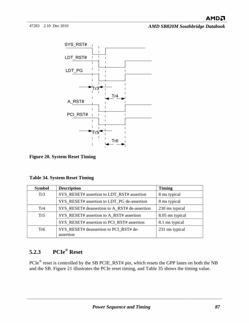
47283 2.10 Dec 2010 AMD SB820M Southbridge Databook
Power Sequence and Timing 87
SYS_RST#
LDT_RST#
LDT_PG
Tr3
Tr4A_RST#
PCI_RST#
Tr5
Tr6
Figure 20. System Reset Timing
Table 34. System Reset Timing
Symbol Description Timing Tr3 SYS_RESET# assertion to LDT_RST# assertion 8 ms typical
SYS_RESET# assertion to LDT_PG de-assertion 8 ms typical Tr4 SYS_RESET# deassertion to A_RST# de-assertion 230 ms typical Tr5 SYS_RESET# assertion to A_RST# assertion 8.05 ms typical
SYS_RESET# assertion to PCI_RST# assertion 8.1 ms typical Tr6 SYS_RESET# deassertion to PCI_RST# de-
assertion 231 ms typical
5.2.3 PCIe® Reset
PCIe® reset is controlled by the SB PCIE_RST# pin, which resets the GPP lanes on both the NB and the SB. Figure 21 illustrates the PCIe reset timing, and Table 35 shows the timing value.
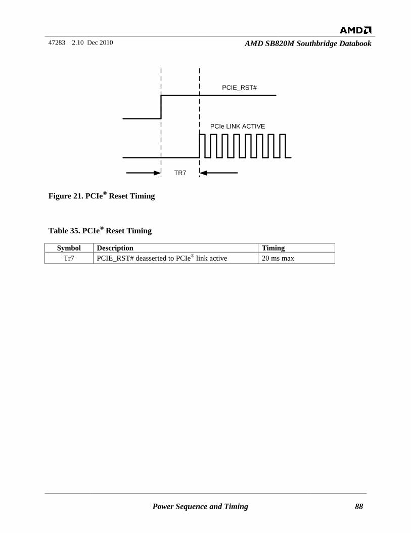
47283 2.10 Dec 2010 AMD SB820M Southbridge Databook
Power Sequence and Timing 88
TR7
PCIE_RST#
PCIe LINK ACTIVE
Figure 21. PCIe® Reset Timing
Table 35. PCIe® Reset Timing
Symbol Description Timing Tr7 PCIE_RST# deasserted to PCIe® link active 20 ms max
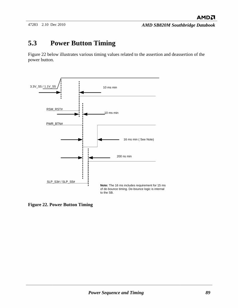
47283 2.10 Dec 2010 AMD SB820M Southbridge Databook
Power Sequence and Timing 89
5.3 Power Button Timing Figure 22 below illustrates various timing values related to the assertion and deassertion of the power button.
PWR_BTN#
RSM_RST#
SLP_S3# / SLP_S5#
3.3V_S5 / 1.1V_S5
10 ms min
10 ms min
200 ns min
16 ms min ( See Note)
Note: The 16 ms includes requirement for 15 ms of de-bounce timing. De-bounce logic is internal to the SB.
Figure 22. Power Button Timing
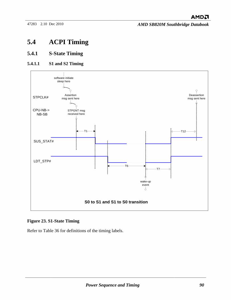
47283 2.10 Dec 2010 AMD SB820M Southbridge Databook
Power Sequence and Timing 90
5.4 ACPI Timing 5.4.1 S-State Timing
5.4.1.1 S1 and S2 Timing
STPCLK#
software initiatesleep here
STPGNT msgreceived here
CPU-NB-> NB-SB
SUS_STAT#
T1
LDT_STP#
wake-upevent
S0 to S1 and S1 to S0 transition
T7
T12
Deassertion msg sent here
Assertion msg sent here
T6
Figure 23. S1-State Timing
Refer to Table 36 for definitions of the timing labels.
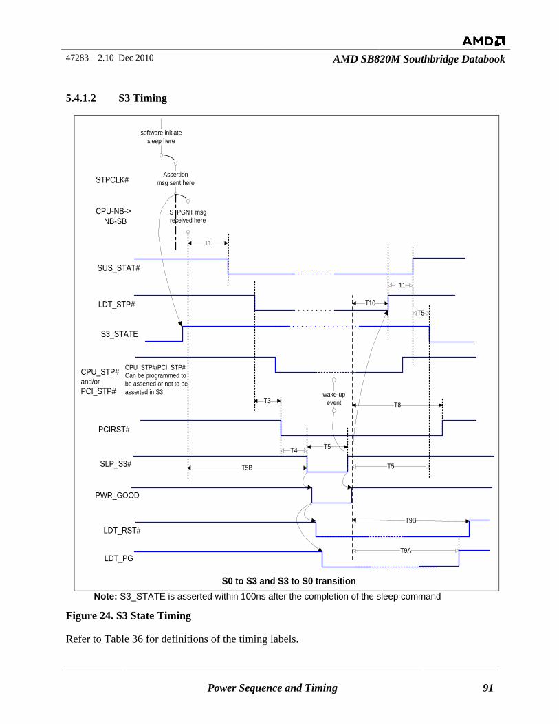
47283 2.10 Dec 2010 AMD SB820M Southbridge Databook
Power Sequence and Timing 91
5.4.1.2 S3 Timing
STPCLK#
software initiatesleep here
STPGNT msgreceived here
CPU-NB-> NB-SB
SUS_STAT#
T1
LDT_STP#
T3wake-up
event
S0 to S3 and S3 to S0 transition
T10
SLP_S3#
PCIRST#
T4
Assertion msg sent here
T5
CPU_STP#and/orPCI_STP#
T5B
T11
PWR_GOOD
CPU_STP#/PCI_STP#Can be programmed to be asserted or not to be asserted in S3
S3_STATE
LDT_RST#
LDT_PG
T8
T5
T5
T9A
T9B
Note: S3_STATE is asserted within 100ns after the completion of the sleep command
Figure 24. S3 State Timing
Refer to Table 36 for definitions of the timing labels.
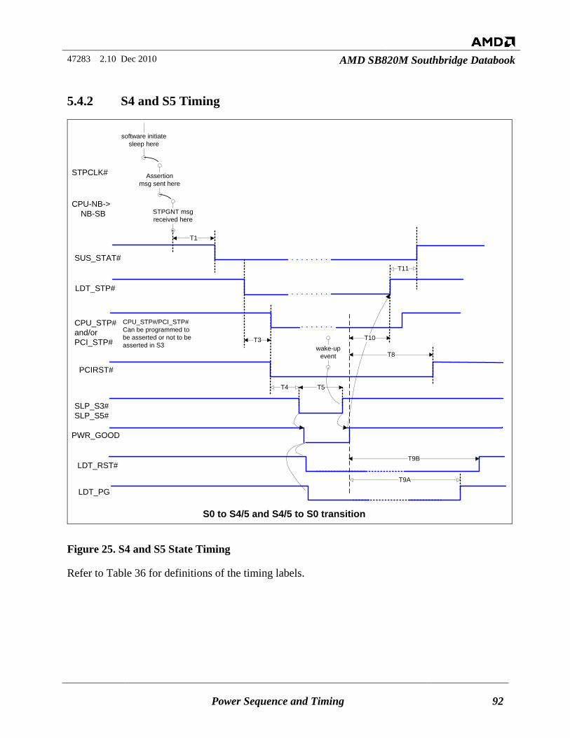
47283 2.10 Dec 2010 AMD SB820M Southbridge Databook
Power Sequence and Timing 92
5.4.2 S4 and S5 Timing
S0 to S4/5 and S4/5 to S0 transition
STPCLK#
software initiatesleep here
STPGNT msgreceived here
CPU-NB-> NB-SB
SUS_STAT#
T1
LDT_STP#
T3wake-up
event
T10
SLP_S3#SLP_S5#
PCIRST#
T4
T8
Assertion msg sent here
T5
T11
PWR_GOOD
CPU_STP#and/orPCI_STP#
CPU_STP#/PCI_STP#Can be programmed to be asserted or not to be asserted in S3
T9B
T9A
LDT_RST#
LDT_PG
Figure 25. S4 and S5 State Timing
Refer to Table 36 for definitions of the timing labels.
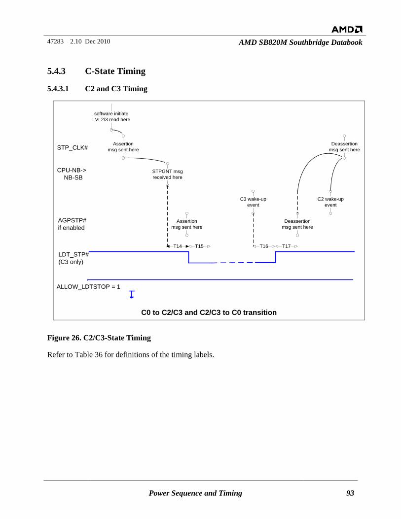
47283 2.10 Dec 2010 AMD SB820M Southbridge Databook
Power Sequence and Timing 93
5.4.3 C-State Timing
5.4.3.1 C2 and C3 Timing
STP_CLK#
software initiateLVL2/3 read here
STPGNT msgreceived here
CPU-NB-> NB-SB
LDT_STP# (C3 only)
T14
C3 wake-upevent
C0 to C2/C3 and C2/C3 to C0 transition
Deassertion msg sent here
Assertion msg sent here
C2 wake-upevent
ALLOW_LDTSTOP = 1
T15 T16 T17
Assertion msg sent here
Deassertion msg sent here
AGPSTP# if enabled
Figure 26. C2/C3-State Timing
Refer to Table 36 for definitions of the timing labels.
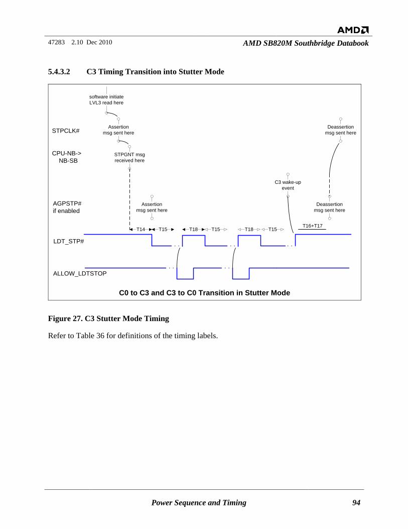
47283 2.10 Dec 2010 AMD SB820M Southbridge Databook
Power Sequence and Timing 94
5.4.3.2 C3 Timing Transition into Stutter Mode
STPCLK#
software initiateLVL3 read here
STPGNT msgreceived here
CPU-NB-> NB-SB
LDT_STP#
T14
C3 wake-upevent
C0 to C3 and C3 to C0 Transition in Stutter Mode
Deassertion msg sent here
Assertion msg sent here
ALLOW_LDTSTOP
T18T15 T15 T18 T15
Assertion msg sent here
Deassertion msg sent here
AGPSTP# if enabled
T16+T17
Figure 27. C3 Stutter Mode Timing
Refer to Table 36 for definitions of the timing labels.
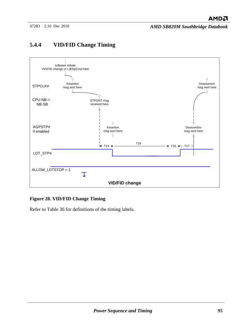
47283 2.10 Dec 2010 AMD SB820M Southbridge Databook
Power Sequence and Timing 95
5.4.4 VID/FID Change Timing
STPCLK#
software initiateVID/FID change or LdtStpCmd here
STPGNT msgreceived here
CPU-NB-> NB-SB
LDT_STP#
T14
VID/FID change
Deassertion msg sent here
Assertion msg sent here
T16 T17T19
AGPSTP# if enabled
Assertion msg sent here
Deassertion msg sent here
ALLOW_LDTSTOP = 1
Figure 28. VID/FID Change Timing
Refer to Table 36 for definitions of the timing labels.
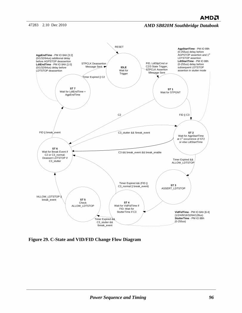
47283 2.10 Dec 2010 AMD SB820M Southbridge Databook
Power Sequence and Timing 96
IDLEWait for Trigger
ST 2Wait for AgpStartTime
at 1st occurrence of ST2 or else LdtStartTime
ST 6Wait for Break Event if
C2 or C3_normal; Deassert LDTSTOP if
C3_stutter
ST 3ASSERT_LDTSTOP
ST 4Wait for VidFidTime if
FID; Wait for StutterTime if C3
Timer Expired && ALLOW_LDTSTOP
ST 1Wait for STPGNT
!ALLOW_LDTSTOP || break_event
STPCLK DeassertionMessage Sent
ST 5Check
ALLOW_LDTSTOP
RESET
FID, LdtStpCmd orC2/3 State Trigger, STPCLK Assertion
Message Sent
Timer Expired && (FID || C3_normal || break_event)
Timer Expired && C3_stutter && !break_event
FID || break_event
ST 7Wait for LdtEndTime +
AgpEndTime
C3 && break_event && break_enable
C3_stutter && !break_event
C2
Timer Expired || C2
FID || C3
VidFidTime - PM IO 8Ah [6:4] (1/2/4/8/16/32/64/128us)StutterTime - PM IO 8Bh (0-255us)
AgpStartTime - PM IO 89h (0-255us) delay before AGPSTOP assertion and 1st LDTSTOP assertionLdtStartTime - PM IO 88h (0-255us) delay before subsequent LDTSTOP assertion in stutter mode
AgpEndTime - PM IO 8Ah [3:2] (0/1/32/64us) additional delay before AGPSTOP deassertionLdtEndTime - PM IO 8Ah [1:0] (0/1/32/64us) delay before LDTSTOP deassertion
Figure 29. C-State and VID/FID Change Flow Diagram
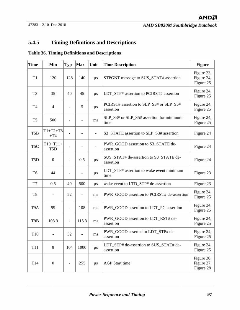
47283 2.10 Dec 2010 AMD SB820M Southbridge Databook
Power Sequence and Timing 97
5.4.5 Timing Definitions and Descriptions
Table 36. Timing Definitions and Descriptions
Time Min Typ Max Unit Time Description Figure
T1 120 128 140 µs STPGNT message to SUS_STAT# assertion Figure 23, Figure 24, Figure 25
T3 35 40 45 µs LDT_STP# assertion to PCIRST# assertion Figure 24, Figure 25
T4 4 - 5 µs PCIRST# assertion to SLP_S3# or SLP_S5# assertion
Figure 24, Figure 25
T5 500 - - ms SLP_S3# or SLP_S5# assertion for minimum time
Figure 24, Figure 25
T5B T1+T2+T3+T4 - - - S3_STATE assertion to SLP_S3# assertion Figure 24
T5C T10+T11+T5D - - - PWR_GOOD assertion to S3_STATE de-
assertion Figure 24
T5D 0 - 0.5 µs SUS_STAT# de-assertion to S3_STATE de-assertion Figure 24
T6 44 - - µs LDT_STP# assertion to wake event minimum time Figure 23
T7 0.5 40 500 µs wake event to LTD_STP# de-assertion Figure 23
T8 - 52 - ms PWR_GOOD assertion to PCIRST# de-assertion Figure 24, Figure 25
T9A 99 - 108 ms PWR_GOOD assertion to LDT_PG assertion Figure 24, Figure 25
T9B 103.9 - 115.3 ms PWR_GOOD assertion to LDT_RST# de-assertion
Figure 24, Figure 25
T10 - 32 - ms PWR_GOOD asserted to LDT_STP# de-assertion
Figure 24, Figure 25
T11 8 104 1000 µs LDT_STP# de-assertion to SUS_STAT# de-assertion
Figure 24, Figure 25
T14 0 - 255 µs AGP Start time Figure 26, Figure 27, Figure 28
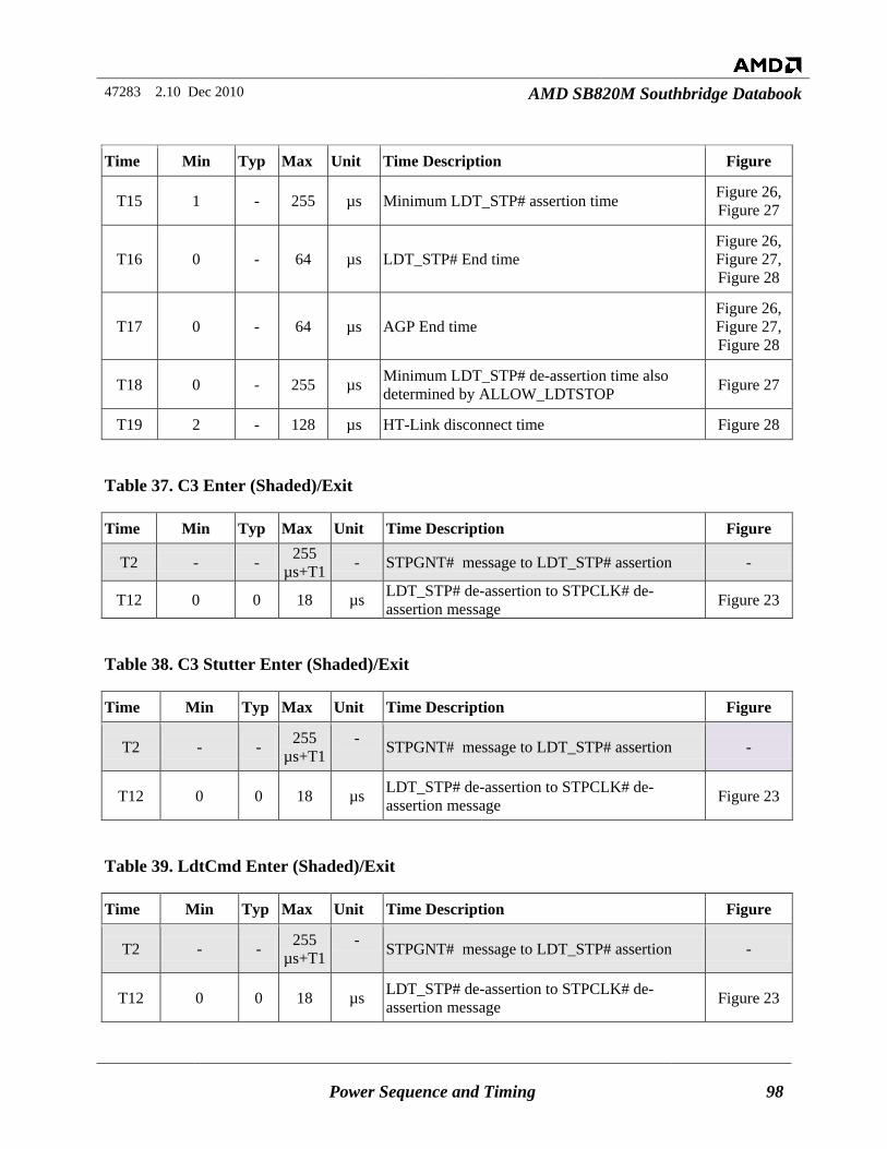
47283 2.10 Dec 2010 AMD SB820M Southbridge Databook
Power Sequence and Timing 98
Time Min Typ Max Unit Time Description Figure
T15 1 - 255 µs Minimum LDT_STP# assertion time Figure 26, Figure 27
T16 0 - 64 µs LDT_STP# End time Figure 26, Figure 27, Figure 28
T17 0 - 64 µs AGP End time Figure 26, Figure 27, Figure 28
T18 0 - 255 µs Minimum LDT_STP# de-assertion time also determined by ALLOW_LDTSTOP Figure 27
T19 2 - 128 µs HT-Link disconnect time Figure 28
Table 37. C3 Enter (Shaded)/Exit
Time Min Typ Max Unit Time Description Figure
T2 - - 255 µs+T1 - STPGNT# message to LDT_STP# assertion -
T12 0 0 18 µs LDT_STP# de-assertion to STPCLK# de-assertion message Figure 23
Table 38. C3 Stutter Enter (Shaded)/Exit
Time Min Typ Max Unit Time Description Figure
T2 - - 255 µs+T1
- STPGNT# message to LDT_STP# assertion -
T12 0 0 18 µs LDT_STP# de-assertion to STPCLK# de-assertion message Figure 23
Table 39. LdtCmd Enter (Shaded)/Exit
Time Min Typ Max Unit Time Description Figure
T2 - - 255 µs+T1
- STPGNT# message to LDT_STP# assertion -
T12 0 0 18 µs LDT_STP# de-assertion to STPCLK# de-assertion message Figure 23
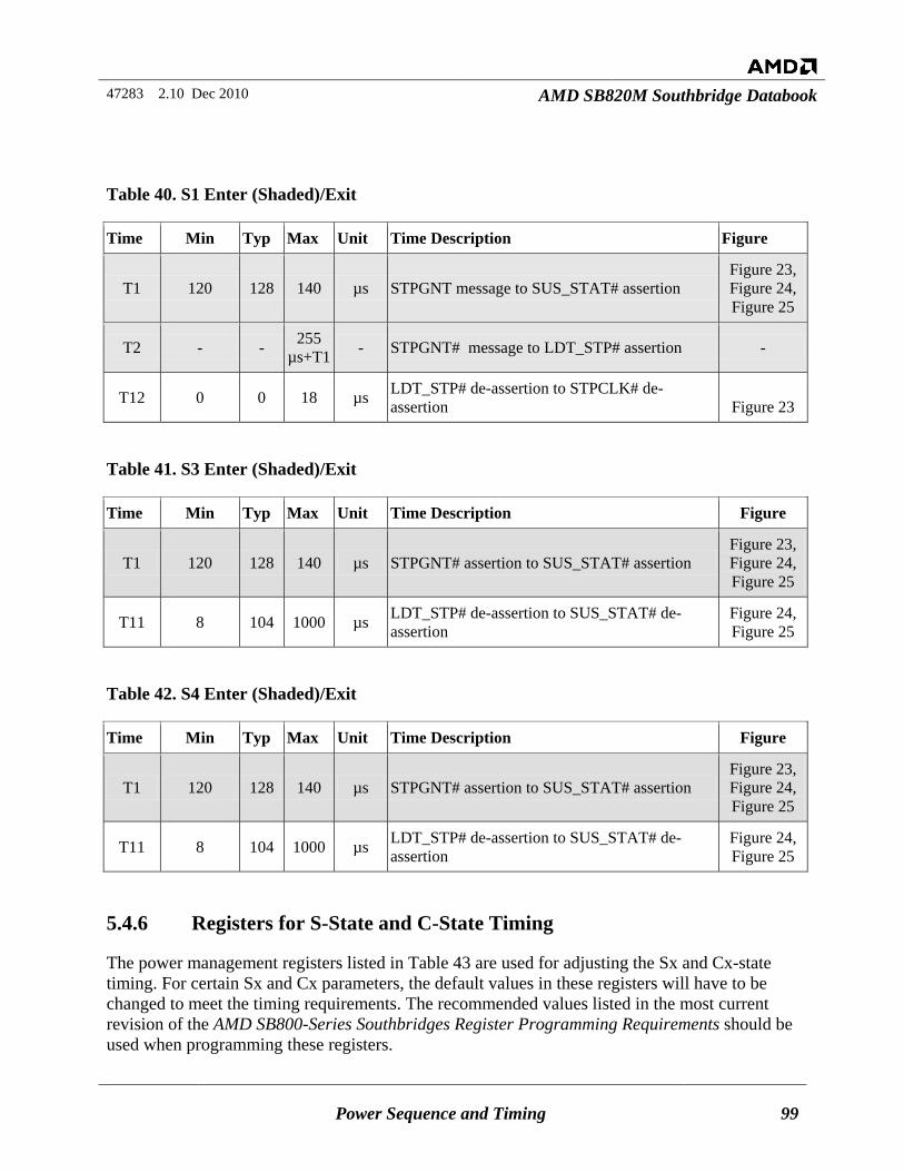
47283 2.10 Dec 2010 AMD SB820M Southbridge Databook
Power Sequence and Timing 99
Table 40. S1 Enter (Shaded)/Exit
Time Min Typ Max Unit Time Description Figure
T1 120 128 140 µs STPGNT message to SUS_STAT# assertion Figure 23, Figure 24, Figure 25
T2 - - 255 µs+T1 - STPGNT# message to LDT_STP# assertion -
T12 0 0 18 µs LDT_STP# de-assertion to STPCLK# de-assertion Figure 23
Table 41. S3 Enter (Shaded)/Exit
Time Min Typ Max Unit Time Description Figure
T1 120 128 140 µs STPGNT# assertion to SUS_STAT# assertion Figure 23, Figure 24, Figure 25
T11 8 104 1000 µs LDT_STP# de-assertion to SUS_STAT# de-assertion
Figure 24, Figure 25
Table 42. S4 Enter (Shaded)/Exit
Time Min Typ Max Unit Time Description Figure
T1 120 128 140 µs STPGNT# assertion to SUS_STAT# assertion Figure 23, Figure 24, Figure 25
T11 8 104 1000 µs LDT_STP# de-assertion to SUS_STAT# de-assertion
Figure 24, Figure 25
5.4.6 Registers for S-State and C-State Timing
The power management registers listed in Table 43 are used for adjusting the Sx and Cx-state timing. For certain Sx and Cx parameters, the default values in these registers will have to be changed to meet the timing requirements. The recommended values listed in the most current revision of the AMD SB800-Series Southbridges Register Programming Requirements should be used when programming these registers.
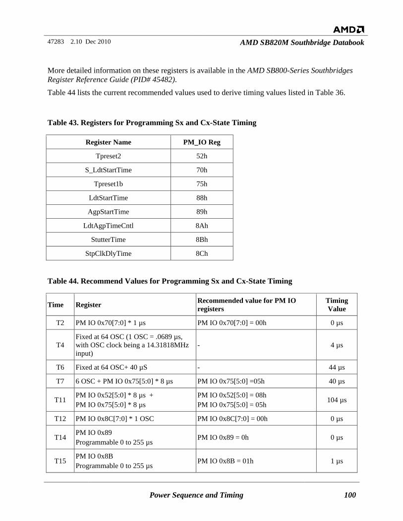
47283 2.10 Dec 2010 AMD SB820M Southbridge Databook
Power Sequence and Timing 100
More detailed information on these registers is available in the AMD SB800-Series Southbridges Register Reference Guide (PID# 45482). Table 44 lists the current recommended values used to derive timing values listed in Table 36.
Table 43. Registers for Programming Sx and Cx-State Timing
Register Name PM_IO Reg
Tpreset2 52h
S_LdtStartTime 70h
Tpreset1b 75h
LdtStartTime 88h
AgpStartTime 89h
LdtAgpTimeCntl 8Ah
StutterTime 8Bh
StpClkDlyTime 8Ch
Table 44. Recommend Values for Programming Sx and Cx-State Timing
Time Register Recommended value for PM IO registers
Timing Value
T2 PM IO 0x70[7:0] * 1 µs PM IO 0x70[7:0] = 00h 0 µs
T4 Fixed at 64 OSC (1 OSC = .0689 µs, with OSC clock being a 14.31818MHz input)
- 4 µs
T6 Fixed at 64 OSC+ 40 µS - 44 µs
T7 6 OSC + PM IO 0x75[5:0] * 8 µs PM IO 0x75[5:0] =05h 40 µs
T11 PM IO 0x52[5:0] * 8 µs + PM IO 0x75[5:0] * 8 µs
PM IO 0x52[5:0] = 08h PM IO 0x75[5:0] = 05h
104 µs
T12 PM IO 0x8C[7:0] * 1 OSC PM IO 0x8C[7:0] = 00h 0 µs
T14 PM IO 0x89 Programmable 0 to 255 µs
PM IO 0x89 = 0h 0 µs
T15 PM IO 0x8B Programmable 0 to 255 µs
PM IO 0x8B = 01h 1 µs
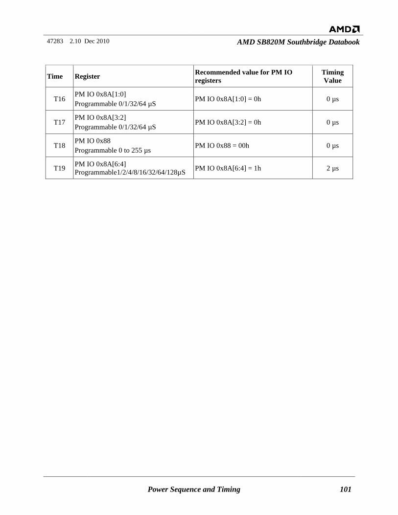
47283 2.10 Dec 2010 AMD SB820M Southbridge Databook
Power Sequence and Timing 101
Time Register Recommended value for PM IO registers
Timing Value
T16 PM IO 0x8A[1:0] Programmable 0/1/32/64 µS
PM IO 0x8A[1:0] = 0h 0 µs
T17 PM IO 0x8A[3:2] Programmable 0/1/32/64 µS
PM IO 0x8A[3:2] = 0h 0 µs
T18 PM IO 0x88 Programmable 0 to 255 µs
PM IO 0x88 = 00h 0 µs
T19 PM IO 0x8A[6:4] Programmable1/2/4/8/16/32/64/128µS PM IO 0x8A[6:4] = 1h 2 µs
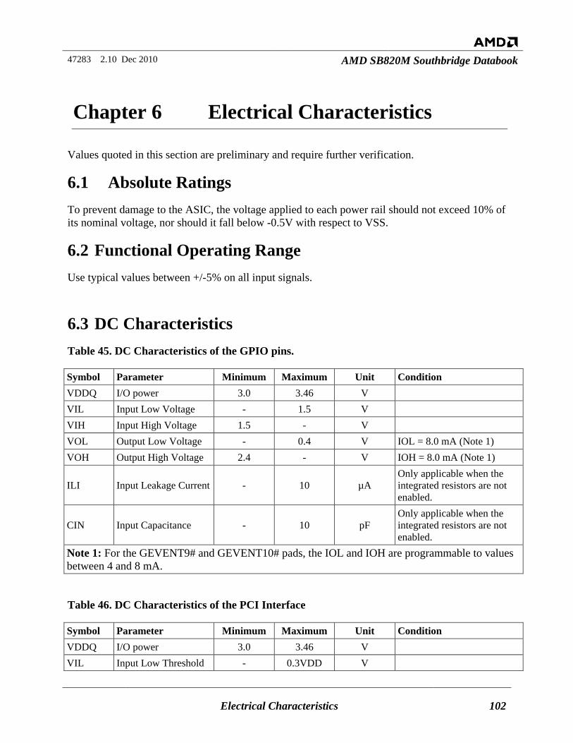
47283 2.10 Dec 2010 AMD SB820M Southbridge Databook
Electrical Characteristics 102
Chapter 6 Electrical Characteristics
Values quoted in this section are preliminary and require further verification.
6.1 Absolute Ratings To prevent damage to the ASIC, the voltage applied to each power rail should not exceed 10% of its nominal voltage, nor should it fall below -0.5V with respect to VSS.
6.2 Functional Operating Range Use typical values between +/-5% on all input signals.
6.3 DC Characteristics Table 45. DC Characteristics of the GPIO pins.
Symbol Parameter Minimum Maximum Unit Condition VDDQ I/O power 3.0 3.46 V VIL Input Low Voltage - 1.5 V VIH Input High Voltage 1.5 - V VOL Output Low Voltage - 0.4 V IOL = 8.0 mA (Note 1) VOH Output High Voltage 2.4 - V IOH = 8.0 mA (Note 1)
ILI Input Leakage Current - 10 µA Only applicable when the integrated resistors are not enabled.
CIN Input Capacitance - 10 pF Only applicable when the integrated resistors are not enabled.
Note 1: For the GEVENT9# and GEVENT10# pads, the IOL and IOH are programmable to values between 4 and 8 mA.
Table 46. DC Characteristics of the PCI Interface
Symbol Parameter Minimum Maximum Unit Condition VDDQ I/O power 3.0 3.46 V VIL Input Low Threshold - 0.3VDD V
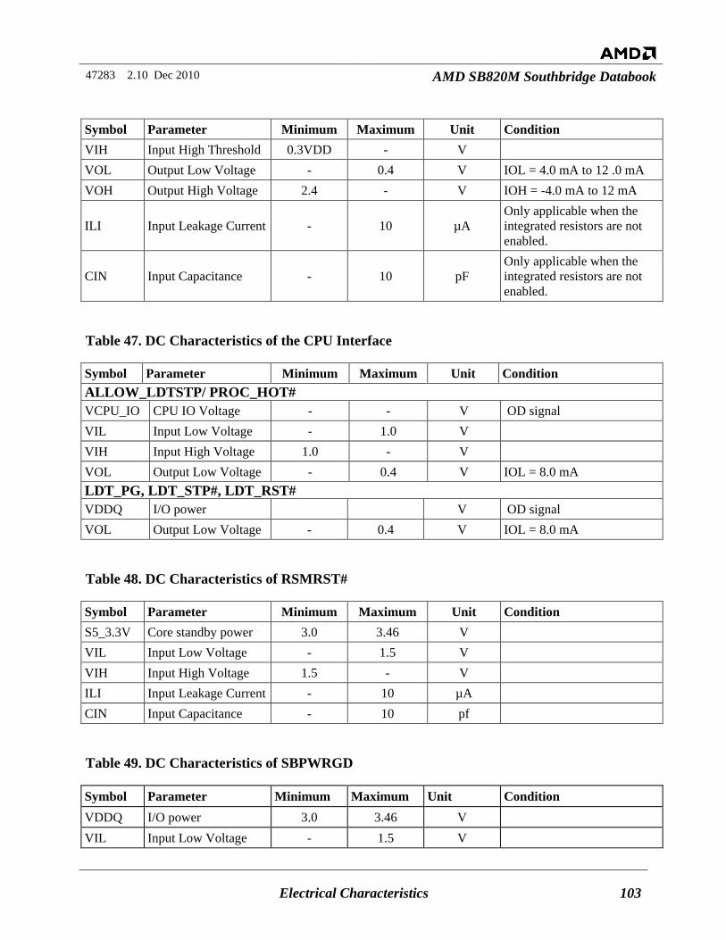
47283 2.10 Dec 2010 AMD SB820M Southbridge Databook
Electrical Characteristics 103
Symbol Parameter Minimum Maximum Unit Condition VIH Input High Threshold 0.3VDD - V VOL Output Low Voltage - 0.4 V IOL = 4.0 mA to 12 .0 mA VOH Output High Voltage 2.4 - V IOH = -4.0 mA to 12 mA
ILI Input Leakage Current - 10 µA Only applicable when the integrated resistors are not enabled.
CIN Input Capacitance - 10 pF Only applicable when the integrated resistors are not enabled.
Table 47. DC Characteristics of the CPU Interface
Symbol Parameter Minimum Maximum Unit Condition ALLOW_LDTSTP/ PROC_HOT# VCPU_IO CPU IO Voltage - - V OD signal VIL Input Low Voltage - 1.0 V VIH Input High Voltage 1.0 - V VOL Output Low Voltage - 0.4 V IOL = 8.0 mA LDT_PG, LDT_STP#, LDT_RST# VDDQ I/O power V OD signal VOL Output Low Voltage - 0.4 V IOL = 8.0 mA
Table 48. DC Characteristics of RSMRST#
Symbol Parameter Minimum Maximum Unit Condition S5_3.3V Core standby power 3.0 3.46 V VIL Input Low Voltage - 1.5 V VIH Input High Voltage 1.5 - V ILI Input Leakage Current - 10 µA CIN Input Capacitance - 10 pf
Table 49. DC Characteristics of SBPWRGD
Symbol Parameter Minimum Maximum Unit Condition VDDQ I/O power 3.0 3.46 V VIL Input Low Voltage - 1.5 V
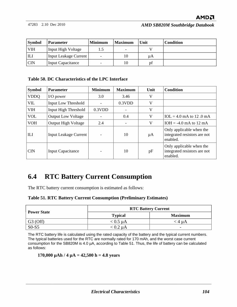
47283 2.10 Dec 2010 AMD SB820M Southbridge Databook
Electrical Characteristics 104
Symbol Parameter Minimum Maximum Unit Condition VIH Input High Voltage 1.5 - V ILI Input Leakage Current - 10 µA CIN Input Capacitance - 10 pf
Table 50. DC Characteristics of the LPC Interface
Symbol Parameter Minimum Maximum Unit Condition VDDQ I/O power 3.0 3.46 V VIL Input Low Threshold - 0.3VDD V VIH Input High Threshold 0.3VDD - V VOL Output Low Voltage - 0.4 V IOL = 4.0 mA to 12 .0 mA VOH Output High Voltage 2.4 - V IOH = -4.0 mA to 12 mA
ILI Input Leakage Current - 10 µA Only applicable when the integrated resistors are not enabled.
CIN Input Capacitance - 10 pF Only applicable when the integrated resistors are not enabled.
6.4 RTC Battery Current Consumption The RTC battery current consumption is estimated as follows:
Table 51. RTC Battery Current Consumption (Preliminary Estimates)
Power State RTC Battery Current
Typical Maximum G3 (Off) < 0.5 µA < 4 µA S0-S5 < 0.2 µA - The RTC battery life is calculated using the rated capacity of the battery and the typical current numbers. The typical batteries used for the RTC are normally rated for 170 mAh, and the worst case current consumption for the SB820M is 4.0 µA, according to Table 51. Thus, the life of battery can be calculated as follows:
170,000 µAh / 4 µA = 42,500 h = 4.8 years
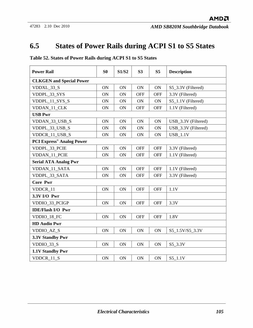
47283 2.10 Dec 2010 AMD SB820M Southbridge Databook
Electrical Characteristics 105
6.5 States of Power Rails during ACPI S1 to S5 States Table 52. States of Power Rails during ACPI S1 to S5 States
Power Rail S0 S1/S2 S3 S5 Description
CLKGEN and Special Power VDDXL_33_S ON ON ON ON S5_3.3V (Filtered) VDDPL_33_SYS ON ON OFF OFF 3.3V (Filtered) VDDPL_11_SYS_S ON ON ON ON S5_1.1V (Filtered) VDDAN_11_CLK ON ON OFF OFF 1.1V (Filtered) USB Pwr VDDAN_33_USB_S ON ON ON ON USB_3.3V (Filtered) VDDPL_33_USB_S ON ON ON ON USB_3.3V (Filtered) VDDCR_11_USB_S ON ON ON ON USB_1.1V PCI Express® Analog Power VDDPL_33_PCIE ON ON OFF OFF 3.3V (Filtered) VDDAN_11_PCIE ON ON OFF OFF 1.1V (Filtered) Serial ATA Analog Pwr VDDAN_11_SATA ON ON OFF OFF 1.1V (Filtered) VDDPL_33_SATA ON ON OFF OFF 3.3V (Filtered) Core Pwr VDDCR_11 ON ON OFF OFF 1.1V 3.3V I/O Pwr VDDIO_33_PCIGP ON ON OFF OFF 3.3V IDE/Flash I/O Pwr VDDIO_18_FC ON ON OFF OFF 1.8V HD Audio Pwr VDDIO_AZ_S ON ON ON ON S5_1.5V/S5_3.3V 3.3V Standby Pwr VDDIO_33_S ON ON ON ON S5_3.3V 1.1V Standby Pwr VDDCR_11_S ON ON ON ON S5_1.1V
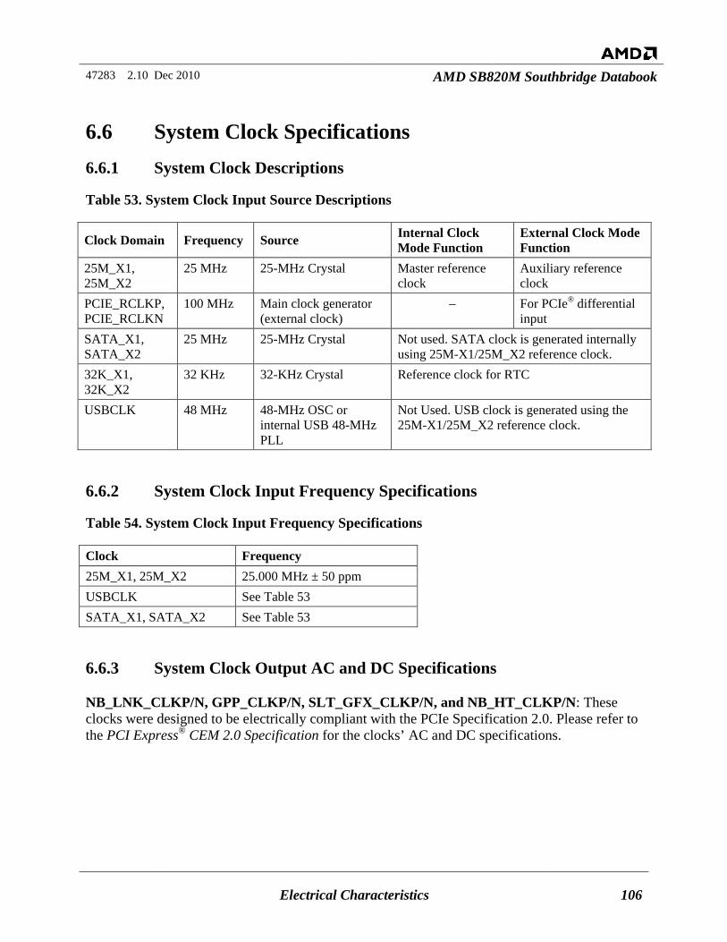
47283 2.10 Dec 2010 AMD SB820M Southbridge Databook
Electrical Characteristics 106
6.6 System Clock Specifications 6.6.1 System Clock Descriptions
Table 53. System Clock Input Source Descriptions
Clock Domain Frequency Source Internal Clock Mode Function
External Clock Mode Function
25M_X1, 25M_X2
25 MHz 25-MHz Crystal Master reference clock
Auxiliary reference clock
PCIE_RCLKP, PCIE_RCLKN
100 MHz Main clock generator (external clock)
– For PCIe® differential input
SATA_X1, SATA_X2
25 MHz 25-MHz Crystal Not used. SATA clock is generated internally using 25M-X1/25M_X2 reference clock.
32K_X1, 32K_X2
32 KHz 32-KHz Crystal Reference clock for RTC
USBCLK 48 MHz 48-MHz OSC or internal USB 48-MHz PLL
Not Used. USB clock is generated using the 25M-X1/25M_X2 reference clock.
6.6.2 System Clock Input Frequency Specifications
Table 54. System Clock Input Frequency Specifications
Clock Frequency 25M_X1, 25M_X2 25.000 MHz ± 50 ppm USBCLK See Table 53 SATA_X1, SATA_X2 See Table 53
6.6.3 System Clock Output AC and DC Specifications
NB_LNK_CLKP/N, GPP_CLKP/N, SLT_GFX_CLKP/N, and NB_HT_CLKP/N: These clocks were designed to be electrically compliant with the PCIe Specification 2.0. Please refer to the PCI Express® CEM 2.0 Specification for the clocks’ AC and DC specifications.
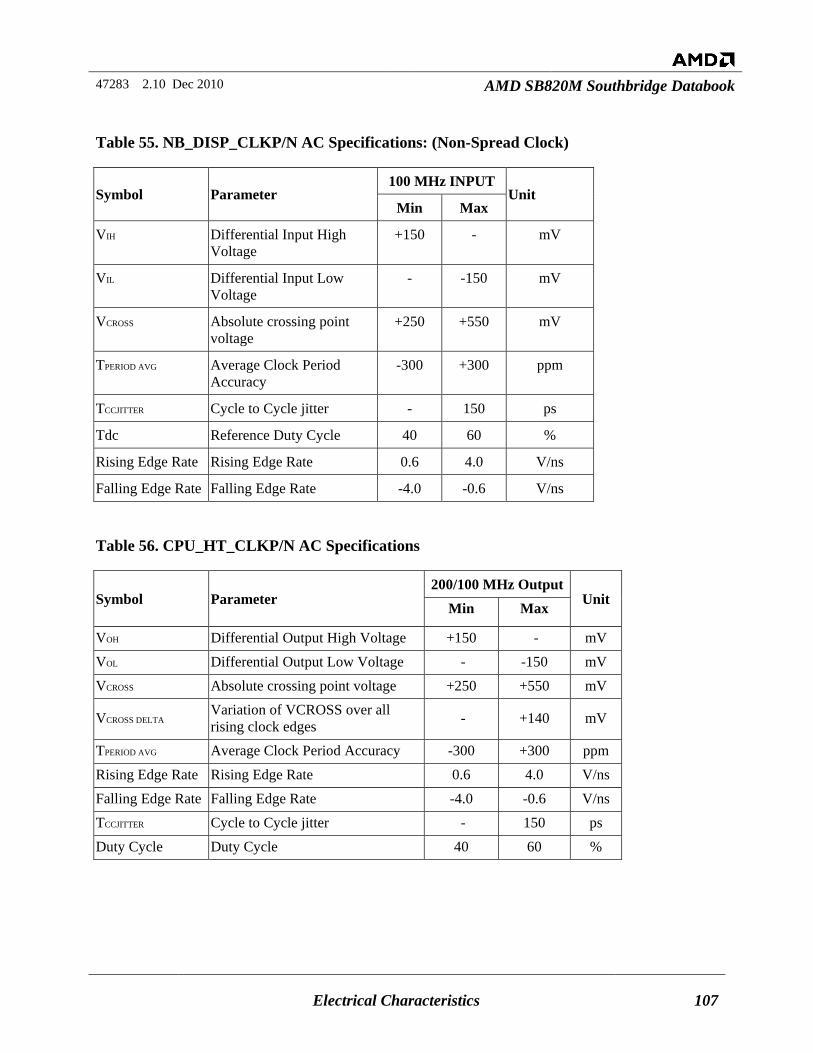
47283 2.10 Dec 2010 AMD SB820M Southbridge Databook
Electrical Characteristics 107
Table 55. NB_DISP_CLKP/N AC Specifications: (Non-Spread Clock)
Symbol Parameter 100 MHz INPUT
Unit Min Max
VIH Differential Input High Voltage
+150 - mV
VIL Differential Input Low Voltage
- -150 mV
VCROSS Absolute crossing point voltage
+250 +550 mV
TPERIOD AVG Average Clock Period Accuracy
-300 +300 ppm
TCCJITTER Cycle to Cycle jitter - 150 ps
Tdc Reference Duty Cycle 40 60 %
Rising Edge Rate Rising Edge Rate 0.6 4.0 V/ns
Falling Edge Rate Falling Edge Rate -4.0 -0.6 V/ns
Table 56. CPU_HT_CLKP/N AC Specifications
Symbol Parameter 200/100 MHz Output
Unit Min Max
VOH Differential Output High Voltage +150 - mV
VOL Differential Output Low Voltage - -150 mV
VCROSS Absolute crossing point voltage +250 +550 mV
VCROSS DELTA Variation of VCROSS over all rising clock edges - +140 mV
TPERIOD AVG Average Clock Period Accuracy -300 +300 ppm
Rising Edge Rate Rising Edge Rate 0.6 4.0 V/ns
Falling Edge Rate Falling Edge Rate -4.0 -0.6 V/ns
TCCJITTER Cycle to Cycle jitter - 150 ps
Duty Cycle Duty Cycle 40 60 %
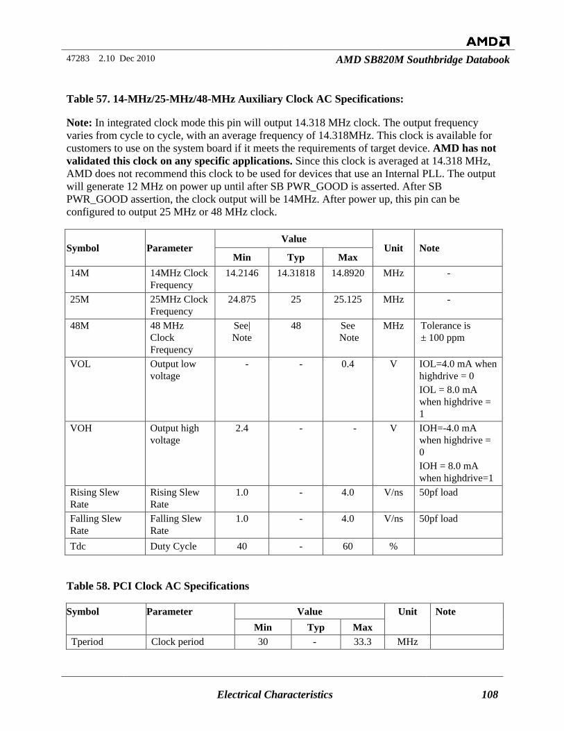
47283 2.10 Dec 2010 AMD SB820M Southbridge Databook
Electrical Characteristics 108
Table 57. 14-MHz/25-MHz/48-MHz Auxiliary Clock AC Specifications:
Note: In integrated clock mode this pin will output 14.318 MHz clock. The output frequency varies from cycle to cycle, with an average frequency of 14.318MHz. This clock is available for customers to use on the system board if it meets the requirements of target device. AMD has not validated this clock on any specific applications. Since this clock is averaged at 14.318 MHz, AMD does not recommend this clock to be used for devices that use an Internal PLL. The output will generate 12 MHz on power up until after SB PWR_GOOD is asserted. After SB PWR_GOOD assertion, the clock output will be 14MHz. After power up, this pin can be configured to output 25 MHz or 48 MHz clock.
Symbol Parameter Value
Unit Note Min Typ Max
14M 14MHz Clock Frequency
14.2146 14.31818 14.8920 MHz -
25M 25MHz Clock Frequency
24.875 25 25.125 MHz -
48M 48 MHz Clock Frequency
See| Note
48 See Note
MHz Tolerance is ± 100 ppm
VOL Output low voltage
- - 0.4 V IOL=4.0 mA when highdrive = 0 IOL = 8.0 mA when highdrive = 1
VOH Output high voltage
2.4 - - V IOH=-4.0 mA when highdrive = 0 IOH = 8.0 mA when highdrive=1
Rising Slew Rate
Rising Slew Rate
1.0 - 4.0 V/ns 50pf load
Falling Slew Rate
Falling Slew Rate
1.0 - 4.0 V/ns 50pf load
Tdc Duty Cycle 40 - 60 %
Table 58. PCI Clock AC Specifications
Symbol Parameter Value Unit Note Min Typ Max
Tperiod Clock period 30 - 33.3 MHz
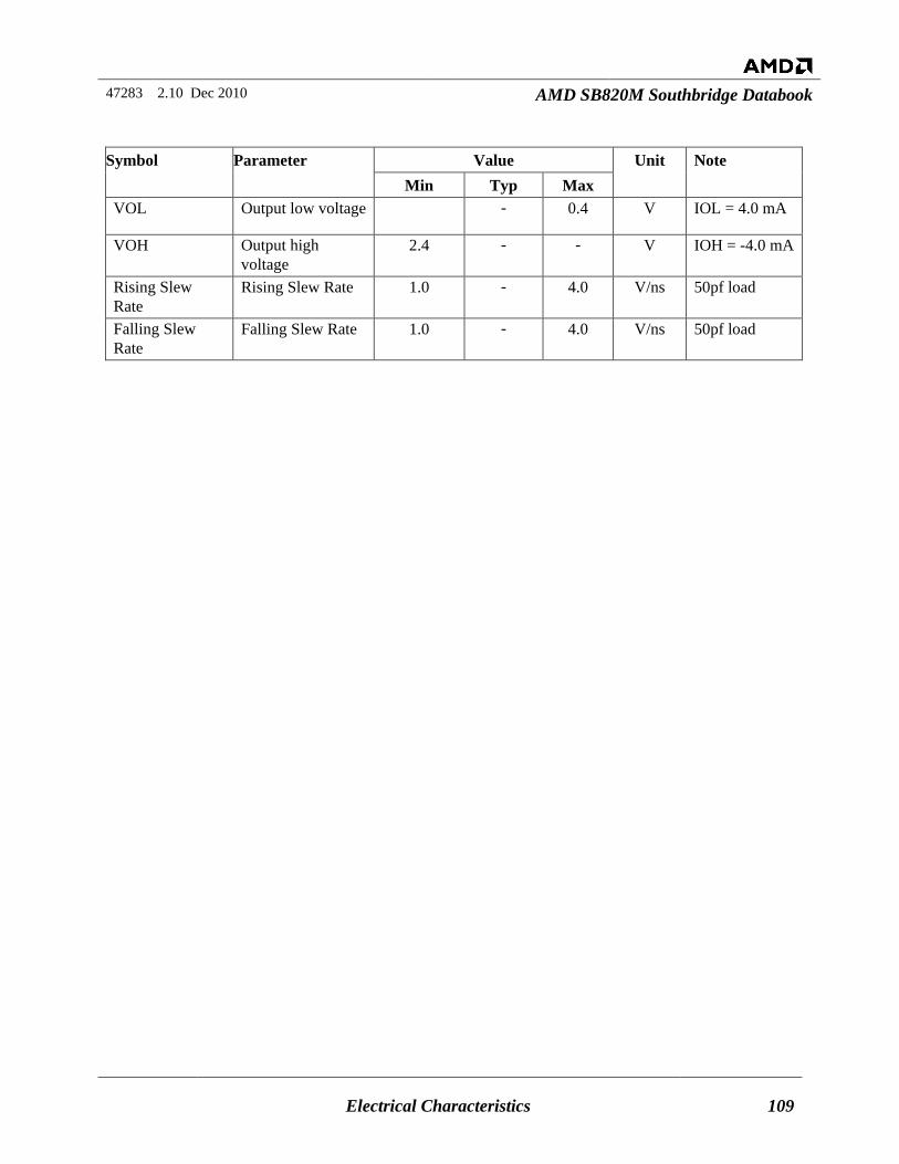
47283 2.10 Dec 2010 AMD SB820M Southbridge Databook
Electrical Characteristics 109
Symbol Parameter Value Unit Note Min Typ Max
VOL Output low voltage - 0.4 V IOL = 4.0 mA
VOH Output high voltage
2.4 - - V IOH = -4.0 mA
Rising Slew Rate
Rising Slew Rate 1.0 - 4.0 V/ns 50pf load
Falling Slew Rate
Falling Slew Rate 1.0 - 4.0 V/ns 50pf load
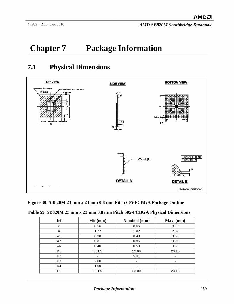
47283 2.10 Dec 2010 AMD SB820M Southbridge Databook
Package Information 110
Chapter 7 Package Information
7.1 Physical Dimensions
Figure 30. SB820M 23 mm x 23 mm 0.8 mm Pitch 605-FCBGA Package Outline
Table 59. SB820M 23 mm x 23 mm 0.8 mm Pitch 605-FCBGA Physical Dimensions
Ref. Min(mm) Nominal (mm) Max. (mm) c 0.56 0.66 0.76 A 1.77 1.92 2.07 A1 0.30 0.40 0.50 A2 0.81 0.86 0.91 φb 0.40 0.50 0.60 D1 22.85 23.00 23.15 D2 - 5.01 - D3 2.00 - - D4 1.00 - - E1 22.85 23.00 23.15
MOD-00115 Doc Rev 02
MOD-00115 REV 02
47283 2.10 Dec 2010 AMD SB820M Southbridge Databook
Package Information 111
Ref. Min(mm) Nominal (mm) Max. (mm) E2 - 6.99 - E3 2.00 - - E4 1.00 - - F1 - 21.60 - F2 - 21.60 -
e (min. pitch) - 0.80 - ddd - - 0.20
7.2 Pressure Specification To avoid damages to the ASIC (die or solder ball joint cracks) caused by improper mechanical assembly of the cooling device, follow the recommendations below: • It is recommended that the maximum load that is evenly applied across the contact area
between the thermal management device and the die does not exceed 6 lbf. Note that a total load of 4-6 lbf is adequate to secure the thermal management device and achieve the lowest thermal contact resistance with a temperature drop across the thermal interface material of no more than 3°C. Also, the surface flatness of the metal spreader should be 0.001 inch/1 inch.
• Pre-test the assembly fixture with a strain gauge to make sure that the flexing of the final assembled board and the pressure applying around the ASIC package will not exceed 600 micron strain under any circumstances.
Ensure that any distortion (bow or twist) of the board after SMT and cooling device assembly is within industry guidelines (IPC/EIA J-STD-001). For measurement method, refer to the industry approved technique described in the manual IPC-TM-650, section 2.4.22.
7.3 Thermal Information This section describes some key thermal parameters of the SB820M. For a detailed discussion on these parameters and other thermal design descriptions including package level thermal data and analysis, please consult the Thermal Design and Analysis Guidelines for the SB800-Series Southbridges, order# 45488.
Table 60. SB820M Thermal Limits
Parameter Minimum Nominal Maximum Unit Note Operating Case Temperature 0 — 105 °C 1
Absolute Rated Junction Temperature — — 125 °C 2
Storage Temperature -40 — 60 °C Ambient Temperature 0 — 45 °C 3
47283 2.10 Dec 2010 AMD SB820M Southbridge Databook
Package Information 112
Parameter Minimum Nominal Maximum Unit Note
Thermal Design Power — See Table 61 — W 4
Notes: 1. The maximum operating case temperature is measured based on the methodology given in the document Thermal Design and Analysis Guidelines for the SB800-Series Southbridges, order # 45488, Chapter 11. This is the temperature at which the functionality of the product is qualified.
2. The maximum absolute rated junction temperature is the junction temperature at which the device can operate without causing damage to the ASIC.
3. The ambient temperature is the temperature of the local intake air to the thermal management device. The maximum ambient temperature is dependent on the heatsink's local ambient conditions as well as the chassis' external ambient temperature. Refer to Chapter 5 in the Thermal Design and Analysis Guidelines for the SB800-Series Southbridges, order # 45488, for heatsink and thermal design guidelines. Refer to Chapter 6 of the above mentioned document for details of the ambient conditions.
4. Thermal Design Power (TDP) is defined as the highest power dissipated while running currently available worst case applications at nominal core voltages. The core voltage was raised to 5% above its nominal value for measuring the ASIC power. Parts specifically screened for higher core power were used for TDP measurement.
Table 61. SB820M Thermal Design Power for Different Platform Configurations
Performance Mainstream Low Power (Mainstream)
Low Power (UltraThin)
Clock Gen Enabled Enabled Enabled Enabled SATA 6Gb/s 3Gb/s 3Gb/s 3Gb/s SATA Ports 6 6 4 2 RAID 0,1 0,1 0,1 N/A FIS-Based Switching N/A N/A N/A N/A
PCIe® Gen 1 GPP 2x1 2x1 N/A N/A
A-Link II x4 x4 x4 x2 USB Ports 14 + 2 14 + 2 10 + 2 8 + 2 33MHz PCI Enabled Enabled N/A N/A TDP 5.3W 4.9W 4.0W 3.4W
47283 2.10 Dec 2010 AMD SB820M Southbridge Databook
Package Information 113
7.4 Reflow Profile A reference reflow profile is given below. Please note the following when using RoHS/lead-free solder (SAC105/305/405 Tin-Silver-Cu):
• The final reflow temperature profile will depend on the type of solder paste and chemistry of flux used in the SMT process. Modifications to the reference reflow profile may be required in order to accommodate the requirements of the other components in the application.
• An oven with 10 heating zones or above is recommended.
• To ensure that the reflow profile meets the target specification on both sides of the board, a different profile and oven recipe for the first and second reflow may be required.
• Mechanical stiffening can be used to minimize board warpage during reflow.
• It is suggested to decrease temperature cooling rate to minimize board warpage.
• This reflow profile applies only to RoHS/lead-free (high temperature) soldering process and it should not be used for eutectic solder packages. Damage may result if this condition is violated.
• Maximum 3 reflows are allowed on the same part.
Table 62. Recommended Board Solder Reflow Profile - RoHS/Lead-Free Solder
Profiling Stage Temperature Process Range
Overall Preheat Room temp to 220°C 2 mins to 4 mins
Soaking Time 130°C to 170°C Typical 60 – 80 seconds
Liquidus 220°C Typical 60 – 80 seconds
Ramp Rate Ramp up and Cooling <2°C / second
Peak Max. 245°C 235°C +/-5 °C
Temperature at peak within 5°C 240°C to 245°C 10 – 30 seconds
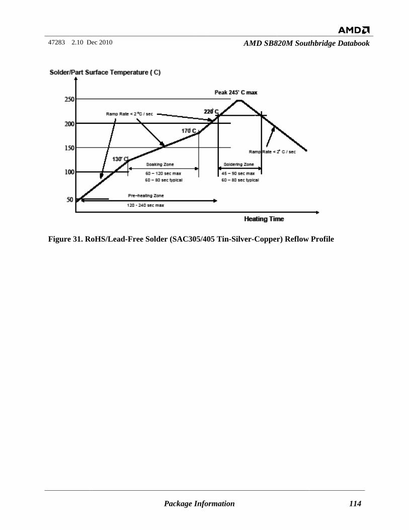
47283 2.10 Dec 2010 AMD SB820M Southbridge Databook
Package Information 114
Figure 31. RoHS/Lead-Free Solder (SAC305/405 Tin-Silver-Copper) Reflow Profile
47283 2.10 Dec 2010 AMD SB820M Southbridge Databook
Testability 115
Chapter 8 Testability
8.1 XOR Chain Test Mode
8.2 Test Control Signals Table 63 below shows the signals used for the integrated test controller of the SB820M.
Table 63. Signals for the Test Controller of the SB820M
Signal Name Description
25M_X1, 25M_X2 25-MHz Reference Clock.
TEST0 Test0 input.
TEST1 Test1 input.
TEST2 Test2 input.
Table 64 shows how Test[2:0] are used to select the normal operation, ASIC debug, or test mode.
Table 64. Test Mode Signals
TEST2 TEST1 TEST0 Test Mode Description 0 0 0 None Normal operation 0 0 1 Reserved Reserved for ASIC debug 0 1 X Test Mode EnableTest Mode 1 X X Reserved Reserved for ASIC debug
When TEST2 is low, a low on TEST1 will reset all test logic and allow TEST0 to choose between normal operation and the reserved debug mode. A high on TEST1 should be followed by a bit sequence on TEST0 to define the test mode into which the SB820M will enter. A new test mode can be entered when a new bit sequence is transmitted. In addition to resetting the test controller asynchronously with TEST1, a bit sequence can also be used to synchronously change the test mode. Table 65 shows the legal bit sequences for TEST0. Note: Once the Test mode or Test mode and sub test mode is entered, Test2 and Test1 should be kept at 0, 1 respectively until the requirement for the Test Mode is completed.
47283 2.10 Dec 2010 AMD SB820M Southbridge Databook
Testability 116
Table 65. TEST0 Bit Sequence
TEST0 bit sequence
Test Mode
11111 Look for first 0 to define a new test mode
00000 Reserved
00001 Alt Pull High Test
00010 Pull Outputs High
00011 Pull Outputs Low
00100 Pull Outputs to Z
00101 XOR Test Mode
Figure 32 illustrates the data timing for the test signals with respect to the OSC clock. Any timing reference referred in this section is assumed to be based on OSC clock running at 25 MHz. The OSC clock can be slowed down to 1 MHz as long as the bit stream applied on TEST0 pin is also in sync with this clock. The 25-MHz OSC clock should be disconnected first. For setting any Test 0 bit sequence, the OSC clock is required only up-to the time the mode set is completed. After this the clock can be stopped and as long as TEST1 and Test2 pins are set to 1, 0 respectively to maintain the selected mode to be active. Note that once TEST1 is set to one, TEST0 needs to be asserted to one for at least 8 clocks before transmitting the test mode bit sequence. The rising of “Internal Test Mode” in the diagram indicates the time when the SB820M enters into test mode.
TEST0
TEST1
Osc
( TEST0 = 1 ) > 8 Osc clocks Bit 4 Bit 1 Bit 2 Bit 3 Bit 0
Internal Test Mode
Figure 32. Test Mode Capturing Sequence Timing
47283 2.10 Dec 2010 AMD SB820M Southbridge Databook
Testability 117
8.2.1 Brief Description of an XOR Chain
A sample of a generic XOR chain is shown in the figure below.
XOR Start Signal
GF
ED
CB
A
Figure 33. A Generic XOR Chain
Pin A is assigned to the output direction, and pins B through F are assigned to the input direction. It can be seen that after all pins from B to F are assigned to logic 0 or 1, a logic change in any one of these pins will toggle the output pin A.
The following is the truth table for the XOR Chain shown in Figure 33. The XOR start signal is assumed to be logic 1.This is an internal signal to the ASIC and is not part of the XOR tree pins listed in Table 66.
Once the inputs are set to the respective value the output pin will reflect the correct value within 200 ns. Note: OSC clock is not required to be running after the mode is already set and the pads are exercised in XOR Tree function.
Table 66. Truth Table for an XOR Chain
Test Vector number
Input Pin G
Input Pin F
Input Pin E
Input Pin D
Input Pin C
Input Pin B
Output Pin A
1 0 0 0 0 0 0 1 2 1 0 0 0 0 0 0 3 1 1 0 0 0 0 1 4 1 1 1 0 0 0 0 5 1 1 1 1 0 0 1 6 1 1 1 1 1 0 0 7 1 1 1 1 1 1 1
47283 2.10 Dec 2010 AMD SB820M Southbridge Databook
Testability 118
8.2.2 Description of the SB820M XOR Chain
During XOR Chain Test Mode, most of the chip pads on the SB820M are connected together using XOR gates as shown in Figure 34. The first input of the chain is connected to a logic level high (internal connection), and all pads (listed in Table 67) are configured as inputs except for the last pad in the chain, which is configured as an output. LDT_STP# is the start of the chain and FC_CE2#/GPIOD150 is the end of the chain. Table 67 lists all pads that are on the SB820M XOR chain, as well as and their order of connection. Pads are chained together in the shown order, i.e., pad number 1 is the first pad on the XOR chain, pad number 2 the second, and so on.
1 ( Tie high Internal to Asic)
pin 1AD6/ROMA12 pin 2 pin 3
pin NFrame#
XOR outFANOUT0/ GPIO3
Figure 34. On-chip XOR Chain connectivity
Table 67. List of Pins on the SB820M XOR Chain and the Order of Connection
XOR # Ball No Pin Name
1 G22 LDT_STP#
2 J24 LDT_RST#
3 J29 LPC_SMI#/GEVENT23#
4 J27 LAD0
5 J25 LDRQ0#
6 G28 LFRAME#
7 H24 LPCCLK0CLK0LPCCLK0
8 H25 LPCCLK1PCCLK1
9 H29 LAD2
10 J26 LAD1
11 G24 KSI_0/GPIO201
12 G25 KSI_1/GPIO202
13 H28 LAD3
XOR # Ball No Pin Name
14 G29 FC_RST#/GPO160
15 F25 EC_PWM0/EC_TIMER0/GPIO197
16 F29 PS2M_DAT/GPIO191
17 F28 PS2KB_CLK/GPIO190
18 F23 SDA2/GPIO194
19 E27 PS2M_CLK/GPIO192
20 E28 KSI_2/GPIO203
21 E29 KSI_3/GPIO204
22 D27 PS2KB_DAT/GPIO189
23 D28 KSI_5/GPIO206
24 D29 KSI_4/GPIO205
25 C28 KSI_7/GPIO208
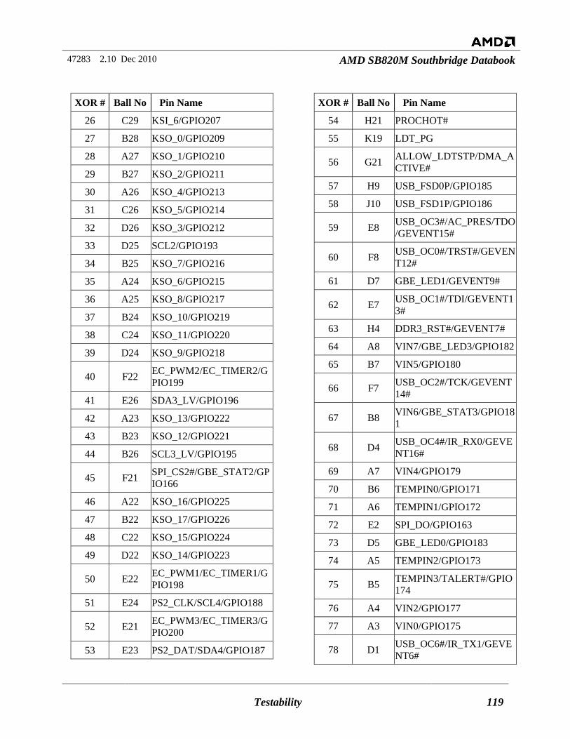
47283 2.10 Dec 2010 AMD SB820M Southbridge Databook
Testability 119
XOR # Ball No Pin Name
26 C29 KSI_6/GPIO207
27 B28 KSO_0/GPIO209
28 A27 KSO_1/GPIO210
29 B27 KSO_2/GPIO211
30 A26 KSO_4/GPIO213
31 C26 KSO_5/GPIO214
32 D26 KSO_3/GPIO212
33 D25 SCL2/GPIO193
34 B25 KSO_7/GPIO216
35 A24 KSO_6/GPIO215
36 A25 KSO_8/GPIO217
37 B24 KSO_10/GPIO219
38 C24 KSO_11/GPIO220
39 D24 KSO_9/GPIO218
40 F22 EC_PWM2/EC_TIMER2/GPIO199
41 E26 SDA3_LV/GPIO196
42 A23 KSO_13/GPIO222
43 B23 KSO_12/GPIO221
44 B26 SCL3_LV/GPIO195
45 F21 SPI_CS2#/GBE_STAT2/GPIO166
46 A22 KSO_16/GPIO225
47 B22 KSO_17/GPIO226
48 C22 KSO_15/GPIO224
49 D22 KSO_14/GPIO223
50 E22 EC_PWM1/EC_TIMER1/GPIO198
51 E24 PS2_CLK/SCL4/GPIO188
52 E21 EC_PWM3/EC_TIMER3/GPIO200
53 E23 PS2_DAT/SDA4/GPIO187
XOR # Ball No Pin Name
54 H21 PROCHOT#
55 K19 LDT_PG
56 G21 ALLOW_LDTSTP/DMA_ACTIVE#
57 H9 USB_FSD0P/GPIO185
58 J10 USB_FSD1P/GPIO186
59 E8 USB_OC3#/AC_PRES/TDO/GEVENT15#
60 F8 USB_OC0#/TRST#/GEVENT12#
61 D7 GBE_LED1/GEVENT9#
62 E7 USB_OC1#/TDI/GEVENT13#
63 H4 DDR3_RST#/GEVENT7#
64 A8 VIN7/GBE_LED3/GPIO182
65 B7 VIN5/GPIO180
66 F7 USB_OC2#/TCK/GEVENT14#
67 B8 VIN6/GBE_STAT3/GPIO181
68 D4 USB_OC4#/IR_RX0/GEVENT16#
69 A7 VIN4/GPIO179
70 B6 TEMPIN0/GPIO171
71 A6 TEMPIN1/GPIO172
72 E2 SPI_DO/GPIO163
73 D5 GBE_LED0/GPIO183
74 A5 TEMPIN2/GPIO173
75 B5 TEMPIN3/TALERT#/GPIO174
76 A4 VIN2/GPIO177
77 A3 VIN0/GPIO175
78 D1 USB_OC6#/IR_TX1/GEVENT6#
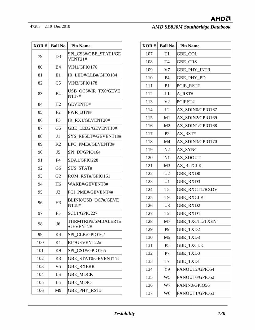
47283 2.10 Dec 2010 AMD SB820M Southbridge Databook
Testability 120
XOR # Ball No Pin Name
79 D3 SPI_CS3#/GBE_STAT1/GEVENT21#
80 B4 VIN1/GPIO176
81 E1 IR_LED#/LLB#/GPIO184
82 C5 VIN3/GPIO178
83 E4 USB_OC5#/IR_TX0/GEVENT17#
84 H2 GEVENT5#
85 F2 PWR_BTN#
86 F3 IR_RX1/GEVENT20#
87 G5 GBE_LED2/GEVENT10#
88 J1 SYS_RESET#/GEVENT19#
89 K2 LPC_PME#/GEVENT3#
90 J5 SPI_DI/GPIO164
91 F4 SDA1/GPIO228
92 G6 SUS_STAT#
93 G2 ROM_RST#/GPIO161
94 H6 WAKE#/GEVENT8#
95 J2 PCI_PME#/GEVENT4#
96 H3 BLINK/USB_OC7#/GEVENT18#
97 F5 SCL1/GPIO227
98 J6 THRMTRIP#/SMBALERT#/GEVENT2#
99 K4 SPI_CLK/GPIO162
100 K1 RI#/GEVENT22#
101 K9 SPI_CS1#/GPIO165
102 K3 GBE_STAT0/GEVENT11#
103 V5 GBE_RXERR
104 L6 GBE_MDCK
105 L5 GBE_MDIO
106 M9 GBE_PHY_RST#
XOR # Ball No Pin Name
107 T1 GBE_COL
108 T4 GBE_CRS
109 V7 GBE_PHY_INTR
110 P4 GBE_PHY_PD
111 P1 PCIE_RST#
112 L1 A_RST#
113 V2 PCIRST#
114 L2 AZ_SDIN0/GPIO167
115 M1 AZ_SDIN2/GPIO169
116 M2 AZ_SDIN1/GPIO168
117 P2 AZ_RST#
118 M4 AZ_SDIN3/GPIO170
119 N2 AZ_SYNC
120 N1 AZ_SDOUT
121 M3 AZ_BITCLK
122 U2 GBE_RXD0
123 U1 GBE_RXD3
124 T5 GBE_RXCTL/RXDV
125 T9 GBE_RXCLK
126 U3 GBE_RXD2
127 T2 GBE_RXD1
128 M7 GBE_TXCTL/TXEN
129 P9 GBE_TXD2
130 M5 GBE_TXD3
131 P5 GBE_TXCLK
132 P7 GBE_TXD0
133 T7 GBE_TXD1
134 Y9 FANOUT2/GPIO54
135 W5 FANOUT0/GPIO52
136 W7 FANIN0/GPIO56
137 W6 FANOUT1/GPIO53
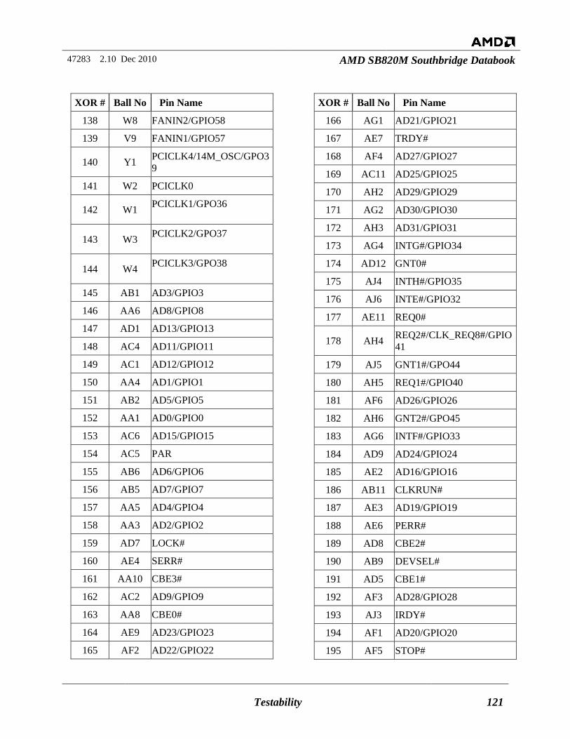
47283 2.10 Dec 2010 AMD SB820M Southbridge Databook
Testability 121
XOR # Ball No Pin Name
138 W8 FANIN2/GPIO58
139 V9 FANIN1/GPIO57
140 Y1 PCICLK4/14M_OSC/GPO39O39
141 W2 PCICLK0PPCICLK0
142 W1 PCICLK1/GPO36CLK1/GPO36
143 W3 PCICLK2/GPO37CLK1CICLK2/G37
144 W4 PCICLK3/GPO38CCICLK3/GPO38
145 AB1 AD3/GPIO3
146 AA6 AD8/GPIO8
147 AD1 AD13/GPIO13
148 AC4 AD11/GPIO11
149 AC1 AD12/GPIO12
150 AA4 AD1/GPIO1
151 AB2 AD5/GPIO5
152 AA1 AD0/GPIO0
153 AC6 AD15/GPIO15
154 AC5 PAR
155 AB6 AD6/GPIO6
156 AB5 AD7/GPIO7
157 AA5 AD4/GPIO4
158 AA3 AD2/GPIO2
159 AD7 LOCK#
160 AE4 SERR#
161 AA10 CBE3#
162 AC2 AD9/GPIO9
163 AA8 CBE0#
164 AE9 AD23/GPIO23
165 AF2 AD22/GPIO22
XOR # Ball No Pin Name
166 AG1 AD21/GPIO21
167 AE7 TRDY#
168 AF4 AD27/GPIO27
169 AC11 AD25/GPIO25
170 AH2 AD29/GPIO29
171 AG2 AD30/GPIO30
172 AH3 AD31/GPIO31
173 AG4 INTG#/GPIO34
174 AD12 GNT0#
175 AJ4 INTH#/GPIO35
176 AJ6 INTE#/GPIO32
177 AE11 REQ0#
178 AH4 REQ2#/CLK_REQ8#/GPIO41
179 AJ5 GNT1#/GPO44
180 AH5 REQ1#/GPIO40
181 AF6 AD26/GPIO26
182 AH6 GNT2#/GPO45
183 AG6 INTF#/GPIO33
184 AD9 AD24/GPIO24
185 AE2 AD16/GPIO16
186 AB11 CLKRUN#
187 AE3 AD19/GPIO19
188 AE6 PERR#
189 AD8 CBE2#
190 AB9 DEVSEL#
191 AD5 CBE1#
192 AF3 AD28/GPIO28
193 AJ3 IRDY#
194 AF1 AD20/GPIO20
195 AF5 STOP#
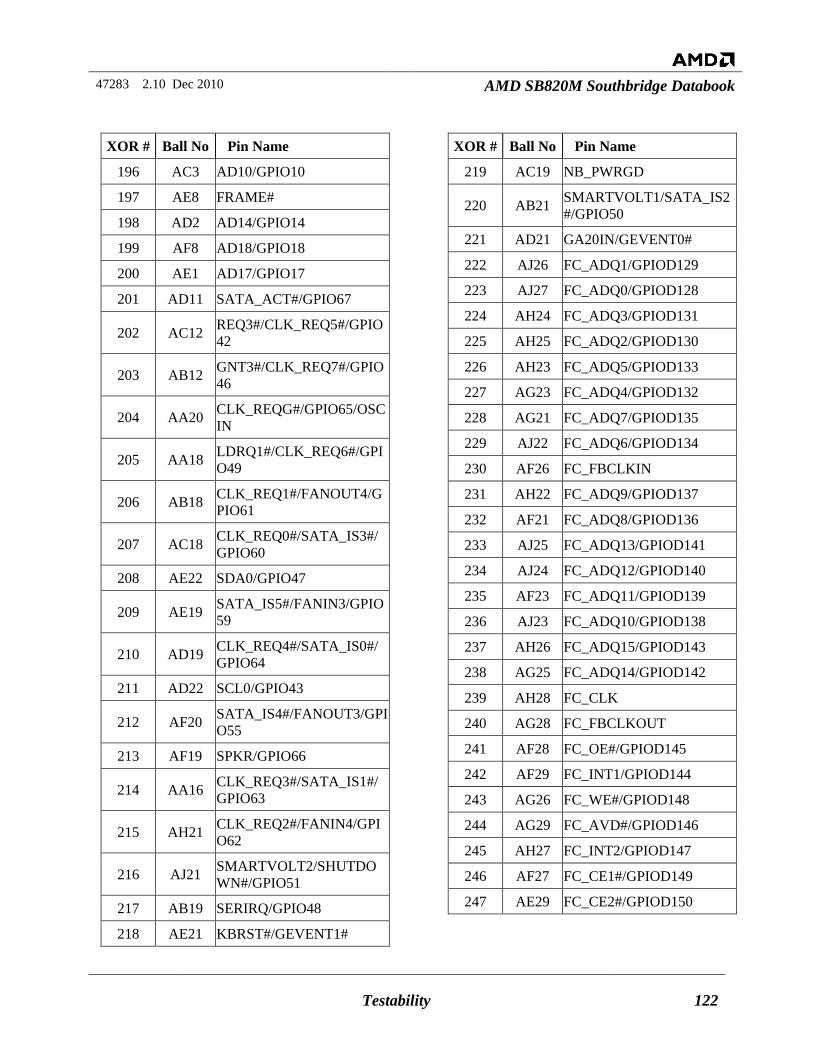
47283 2.10 Dec 2010 AMD SB820M Southbridge Databook
Testability 122
XOR # Ball No Pin Name
196 AC3 AD10/GPIO10
197 AE8 FRAME#
198 AD2 AD14/GPIO14
199 AF8 AD18/GPIO18
200 AE1 AD17/GPIO17
201 AD11 SATA_ACT#/GPIO67
202 AC12 REQ3#/CLK_REQ5#/GPIO42
203 AB12 GNT3#/CLK_REQ7#/GPIO46
204 AA20 CLK_REQG#/GPIO65/OSCIN
205 AA18 LDRQ1#/CLK_REQ6#/GPIO49
206 AB18 CLK_REQ1#/FANOUT4/GPIO61
207 AC18 CLK_REQ0#/SATA_IS3#/GPIO60
208 AE22 SDA0/GPIO47
209 AE19 SATA_IS5#/FANIN3/GPIO59
210 AD19 CLK_REQ4#/SATA_IS0#/GPIO64
211 AD22 SCL0/GPIO43
212 AF20 SATA_IS4#/FANOUT3/GPIO55
213 AF19 SPKR/GPIO66
214 AA16 CLK_REQ3#/SATA_IS1#/GPIO63
215 AH21 CLK_REQ2#/FANIN4/GPIO62
216 AJ21 SMARTVOLT2/SHUTDOWN#/GPIO51
217 AB19 SERIRQ/GPIO48
218 AE21 KBRST#/GEVENT1#
XOR # Ball No Pin Name
219 AC19 NB_PWRGD
220 AB21 SMARTVOLT1/SATA_IS2#/GPIO50
221 AD21 GA20IN/GEVENT0#
222 AJ26 FC_ADQ1/GPIOD129
223 AJ27 FC_ADQ0/GPIOD128
224 AH24 FC_ADQ3/GPIOD131
225 AH25 FC_ADQ2/GPIOD130
226 AH23 FC_ADQ5/GPIOD133
227 AG23 FC_ADQ4/GPIOD132
228 AG21 FC_ADQ7/GPIOD135
229 AJ22 FC_ADQ6/GPIOD134
230 AF26 FC_FBCLKIN
231 AH22 FC_ADQ9/GPIOD137
232 AF21 FC_ADQ8/GPIOD136
233 AJ25 FC_ADQ13/GPIOD141
234 AJ24 FC_ADQ12/GPIOD140
235 AF23 FC_ADQ11/GPIOD139
236 AJ23 FC_ADQ10/GPIOD138
237 AH26 FC_ADQ15/GPIOD143
238 AG25 FC_ADQ14/GPIOD142
239 AH28 FC_CLK
240 AG28 FC_FBCLKOUT
241 AF28 FC_OE#/GPIOD145
242 AF29 FC_INT1/GPIOD144
243 AG26 FC_WE#/GPIOD148
244 AG29 FC_AVD#/GPIOD146
245 AH27 FC_INT2/GPIOD147
246 AF27 FC_CE1#/GPIOD149
247 AE29 FC_CE2#/GPIOD150
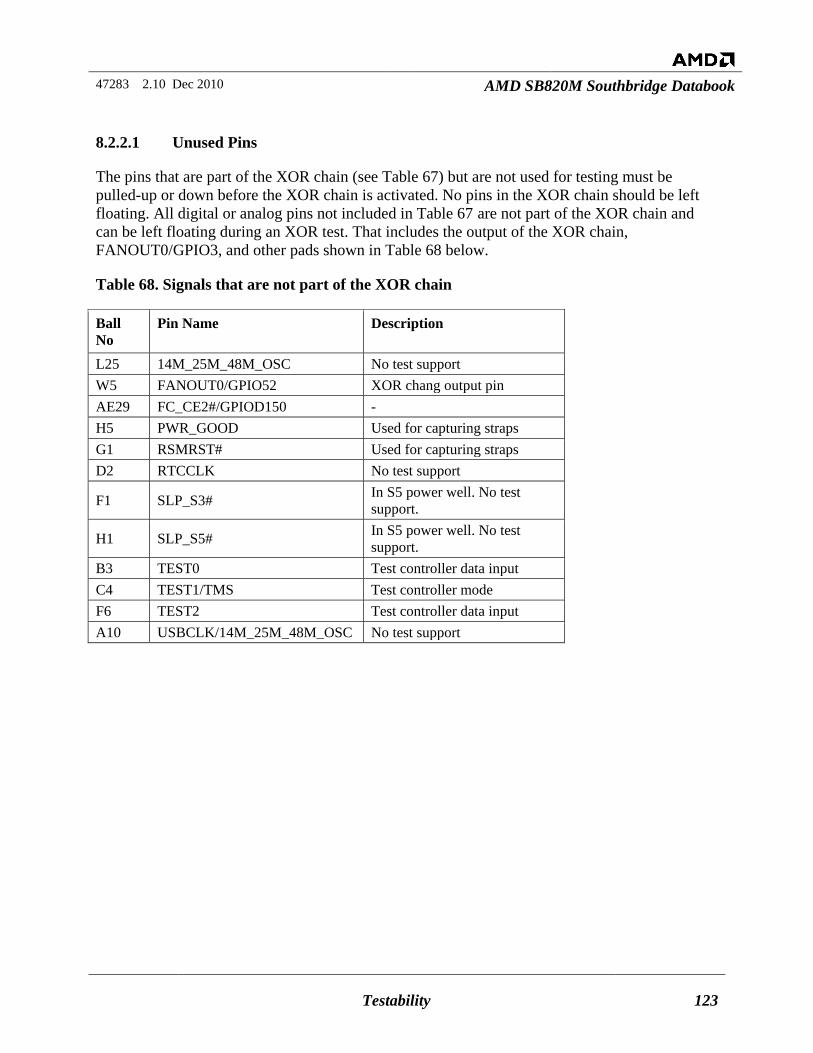
47283 2.10 Dec 2010 AMD SB820M Southbridge Databook
Testability 123
8.2.2.1 Unused Pins
The pins that are part of the XOR chain (see Table 67) but are not used for testing must be pulled-up or down before the XOR chain is activated. No pins in the XOR chain should be left floating. All digital or analog pins not included in Table 67 are not part of the XOR chain and can be left floating during an XOR test. That includes the output of the XOR chain, FANOUT0/GPIO3, and other pads shown in Table 68 below.
Table 68. Signals that are not part of the XOR chain
Ball No
Pin Name Description
L25 14M_25M_48M_OSCC No test support W5 FANOUT0/GPIO52 XOR chang output pin AE29 FC_CE2#/GPIOD150 - H5 PWR_GOOD Used for capturing straps G1 RSMRST# Used for capturing straps D2 RTCCLK No test support
F1 SLP_S3# In S5 power well. No test support.
H1 SLP_S5# In S5 power well. No test support.
B3 TEST0 Test controller data input C4 TEST1/TMS Test controller mode F6 TEST2 Test controller data input A10 USBCLK/14M_25M_48M_OSC No test support
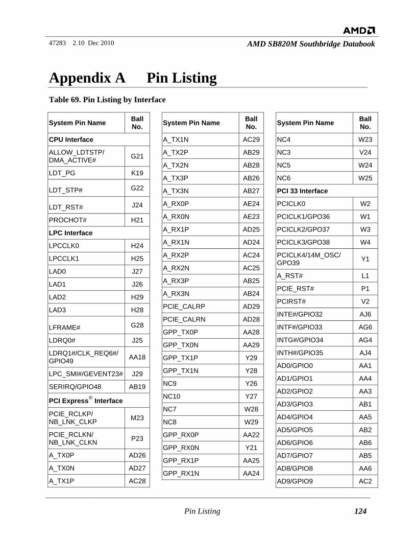
47283 2.10 Dec 2010 AMD SB820M Southbridge Databook
Pin Listing 124
Appendix A Pin Listing Table 69. Pin Listing by Interface
System Pin Name Ball No.
CPU Interface
ALLOW_LDTSTP/ DMA_ACTIVE# G21
LDT_PG K19
LDT_STP# G22
LDT_RST# J24
PROCHOT# H21
LPC Interface
LPCCLK0 H24
LPCCLK1 H25
LAD0 J27
LAD1 J26
LAD2 H29
LAD3 H28
LFRAME# G28
LDRQ0# J25
LDRQ1#/CLK_REQ6#/ GPIO49 AA18
LPC_SMI#/GEVENT23# J29
SERIRQ/GPIO48 AB19
PCI Express® Interface
PCIE_RCLKP/ NB_LNK_CLKP M23
PCIE_RCLKN/ NB_LNK_CLKN P23
A_TX0P AD26
A_TX0N AD27
A_TX1P AC28
System Pin Name Ball No.
A_TX1N AC29
A_TX2P AB29
A_TX2N AB28
A_TX3P AB26
A_TX3N AB27
A_RX0P AE24
A_RX0N AE23
A_RX1P AD25
A_RX1N AD24
A_RX2P AC24
A_RX2N AC25
A_RX3P AB25
A_RX3N AB24
PCIE_CALRP AD29
PCIE_CALRN AD28
GPP_TX0P AA28
GPP_TX0N AA29
GPP_TX1P Y29
GPP_TX1N Y28
NC9 Y26
NC10 Y27
NC7 W28
NC8 W29
GPP_RX0P AA22
GPP_RX0N Y21
GPP_RX1P AA25
GPP_RX1N AA24
System Pin Name Ball No.
NC4 W23
NC3 V24
NC5 W24
NC6 W25
PCI 33 Interface
PCICLK0 W2
PCICLK1/GPO36 W1
PCICLK2/GPO37 W3
PCICLK3/GPO38 W4
PCICLK4/14M_OSC/ GPO39 Y1
A_RST# L1
PCIE_RST# P1
PCIRST# V2
INTE#/GPIO32 AJ6
INTF#/GPIO33 AG6
INTG#/GPIO34 AG4
INTH#/GPIO35 AJ4
AD0/GPIO0 AA1
AD1/GPIO1 AA4
AD2/GPIO2 AA3
AD3/GPIO3 AB1
AD4/GPIO4 AA5
AD5/GPIO5 AB2
AD6/GPIO6 AB6
AD7/GPIO7 AB5
AD8/GPIO8 AA6
AD9/GPIO9 AC2
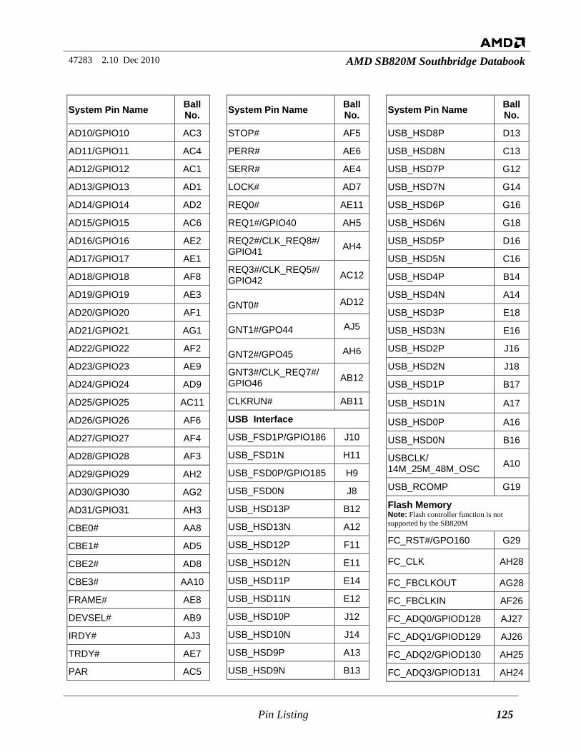
47283 2.10 Dec 2010 AMD SB820M Southbridge Databook
Pin Listing 125
System Pin Name Ball No.
AD10/GPIO10 AC3
AD11/GPIO11 AC4
AD12/GPIO12 AC1
AD13/GPIO13 AD1
AD14/GPIO14 AD2
AD15/GPIO15 AC6
AD16/GPIO16 AE2
AD17/GPIO17 AE1
AD18/GPIO18 AF8
AD19/GPIO19 AE3
AD20/GPIO20 AF1
AD21/GPIO21 AG1
AD22/GPIO22 AF2
AD23/GPIO23 AE9
AD24/GPIO24 AD9
AD25/GPIO25 AC11
AD26/GPIO26 AF6
AD27/GPIO27 AF4
AD28/GPIO28 AF3
AD29/GPIO29 AH2
AD30/GPIO30 AG2
AD31/GPIO31 AH3
CBE0# AA8
CBE1# AD5
CBE2# AD8
CBE3# AA10
FRAME# AE8
DEVSEL# AB9
IRDY# AJ3
TRDY# AE7
PAR AC5
System Pin Name Ball No.
STOP# AF5
PERR# AE6
SERR# AE4
LOCK# AD7
REQ0# AE11
REQ1#/GPIO40 AH5
REQ2#/CLK_REQ8#/ GPIO41 AH4
REQ3#/CLK_REQ5#/ GPIO42 AC12
GNT0# AD12
GNT1#/GPO44 AJ5
GNT2#/GPO45 AH6
GNT3#/CLK_REQ7#/ GPIO46 AB12
CLKRUN# AB11
USB Interface
USB_FSD1P/GPIO186 J10
USB_FSD1N H11
USB_FSD0P/GPIO185 H9
USB_FSD0N J8
USB_HSD13P B12
USB_HSD13N A12
USB_HSD12P F11
USB_HSD12N E11
USB_HSD11P E14
USB_HSD11N E12
USB_HSD10P J12
USB_HSD10N J14
USB_HSD9P A13
USB_HSD9N B13
System Pin Name Ball No.
USB_HSD8P D13
USB_HSD8N C13
USB_HSD7P G12
USB_HSD7N G14
USB_HSD6P G16
USB_HSD6N G18
USB_HSD5P D16
USB_HSD5N C16
USB_HSD4P B14
USB_HSD4N A14
USB_HSD3P E18
USB_HSD3N E16
USB_HSD2P J16
USB_HSD2N J18
USB_HSD1P B17
USB_HSD1N A17
USB_HSD0P A16
USB_HSD0N B16
USBCLK/ 14M_25M_48M_OSC A10
USB_RCOMP G19
Flash Memory Note: Flash controller function is not supported by the SB820M
FC_RST#/GPO160 G29
FC_CLK AH28
FC_FBCLKOUT AG28
FC_FBCLKIN AF26
FC_ADQ0/GPIOD128 AJ27
FC_ADQ1/GPIOD129 AJ26
FC_ADQ2/GPIOD130 AH25
FC_ADQ3/GPIOD131 AH24
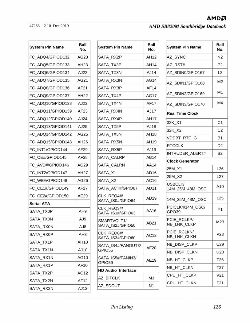
47283 2.10 Dec 2010 AMD SB820M Southbridge Databook
Pin Listing 126
System Pin Name Ball No.
FC_ADQ4/GPIOD132 AG23
FC_ADQ5/GPIOD133 AH23
FC_ADQ6/GPIOD134 AJ22
FC_ADQ7/GPIOD135 AG21
FC_ADQ8/GPIOD136 AF21
FC_ADQ9/GPIOD137 AH22
FC_ADQ10/GPIOD138 AJ23
FC_ADQ11/GPIOD139 AF23
FC_ADQ12/GPIOD140 AJ24
FC_ADQ13/GPIOD141 AJ25
FC_ADQ14/GPIOD142 AG25
FC_ADQ15/GPIOD143 AH26
FC_INT1/GPIOD144 AF29
FC_OE#/GPIOD145 AF28
FC_AVD#/GPIOD146 AG29
FC_INT2/GPIOD147 AH27
FC_WE#/GPIOD148 AG26
FC_CE1#/GPIOD149 AF27
FC_CE2#/GPIOD150 AE29
Serial ATA
SATA_TX0P AH9
SATA_TX0N AJ9
SATA_RX0N AJ8
SATA_RX0P AH8
SATA_TX1P AH10
SATA_TX1N AJ10
SATA_RX1N AG10
SATA_RX1P AF10
SATA_TX2P AG12
SATA_TX2N AF12
SATA_RX2N AJ12
System Pin Name Ball No.
SATA_RX2P AH12
SATA_TX3P AH14
SATA_TX3N AJ14
SATA_RX3N AG14
SATA_RX3P AF14
SATA_TX4P AG17
SATA_TX4N AF17
SATA_RX4N AJ17
SATA_RX4P AH17
SATA_TX5P AJ18
SATA_TX5N AH18
SATA_RX5N AH19
SATA_RX5P AJ19
SATA_CALRP AB14
SATA_CALRN AA14
SATA_X1 AD16
SATA_X2 AC16
SATA_ACT#/GPIO67 AD11
CLK_REQ4#/ SATA_IS0#/GPIO64 AD19
CLK_REQ3#/ SATA_IS1#/GPIO63 AA16
SMARTVOLT1/ SATA_IS2#/GPIO50 AB21
CLK_REQ0#/ SATA_IS3#/GPIO60 AC18
SATA_IS4#/FANOUT3/GPIO55 AF20
SATA_IS5#/FANIN3/ GPIO59 AE19
HD Audio Interface
AZ_BITCLK M3
AZ_SDOUT N1
System Pin Name Ball No.
AZ_SYNC N2
AZ_RST# P2
AZ_SDIN0/GPIO167 L2
AZ_SDIN1/GPIO168 M2
AZ_SDIN2/GPIO169 M1
AZ_SDIN3/GPIO170 M4
Real Time Clock
32K_X1 C1
32K_X2 C2
VDDBT_RTC_G B1
RTCCLK D2
INTRUDER_ALERT# B2
Clock Generator
25M_X1 L26
25M_X2 L27
USBCLK/ 14M_25M_48M_OSC A10
14M_25M_48M_OSC L25
PCICLK4/14M_OSC/ GPO39 Y1
PCIE_RCLKP/ NB_LNK_CLKP M23
PCIE_RCLKN/ NB_LNK_CLKN P23
NB_DISP_CLKP U29
NB_DISP_CLKN U28
NB_HT_CLKP T26
NB_HT_CLKN T27
CPU_HT_CLKP V21
CPU_HT_CLKN T21
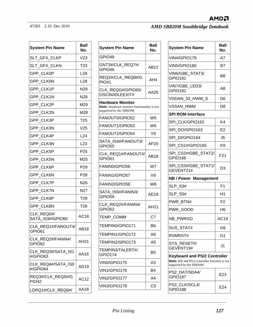
47283 2.10 Dec 2010 AMD SB820M Southbridge Databook
Pin Listing 127
System Pin Name Ball No.
SLT_GFX_CLKP V23
SLT_GFX_CLKN T23
GPP_CLK0P L29
GPP_CLK0N L28
GPP_CLK1P N29
GPP_CLK1N N28
GPP_CLK2P M29
GPP_CLK2N M28
GPP_CLK3P T25
GPP_CLK3N V25
GPP_CLK4P L24
GPP_CLK4N L23
GPP_CLK5P P25
GPP_CLK5N M25
GPP_CLK6P P29
GPP_CLK6N P28
GPP_CLK7P N26
GPP_CLK7N N27
GPP_CLK8P T29
GPP_CLK8N T28
CLK_REQ0#/ SATA_IS3#/GPIO60 AC18
CLK_REQ1#/FANOUT4/GPIO61 AB18
CLK_REQ2#/FANIN4/ GPIO62 AH21
CLK_REQ3#/SATA_IS1#/GPIO63 AA16
CLK_REQ4#/SATA_IS0#/GPIO64 AD19
REQ3#/CLK_REQ5#/GPIO42 AC12
LDRQ1#/CLK_REQ6#/ AA18
System Pin Name Ball No.
GPIO49
GNT3#/CLK_REQ7#/ GPIO46 AB12
REQ2#/CLK_REQ8#/GPIO41 AH4
CLK_REQG#/GPIO65/ OSCIN/IDLEEXIT# AA20
Hardware Monitor Note: Hardware monitor functionality is not supported by the SB820M
FANOUT0/GPIO52 W5
FANOUT1/GPIO53 W6
FANOUT2/GPIO54 Y9
SATA_IS4#/FANOUT3/GPIO55 AF20
CLK_REQ1#/FANOUT4/GPIO61 AB18
FANIN0/GPIO56 W7
FANIN1/GPIO57 V9
FANIN2/GPIO58 W8
SATA_IS5#/FANIN3/ GPIO59 AE19
CLK_REQ2#/FANIN4/ GPIO62 AH21
TEMP_COMM C7
TEMPIN0/GPIO171 B6
TEMPIN1/GPIO172 A6
TEMPIN2/GPIO173 A5
TEMPIN3/TALERT#/ GPIO174 B5
VIN0/GPIO175 A3
VIN1/GPIO176 B4
VIN2/GPIO177 A4
VIN3/GPIO178 C5
System Pin Name Ball No.
VIN4/GPIO179 A7
VIN5/GPIO180 B7
VIN6/GBE_STAT3/ GPIO181 B8
VIN7/GBE_LED3/ GPIO182 A8
VDDAN_33_HWM_S D6
VSSAN_HWM D8
SPI ROM Interface
SPI_CLK/GPIO162 K4
SPI_DO/GPIO163 E2
SPI_DI/GPIO164 J5
SPI_CS1#/GPIO165 K9
SPI_CS2#/GBE_STAT2/GPIO166 F21
SPI_CS3#/GBE_STAT1/GEVENT21# D3
NB / Power Management
SLP_S3# F1
SLP_S5# H1
PWR_BTN# F2
PWR_GOOD H5
NB_PWRGD AC19
SUS_STAT# G6
RSMRST# G1
SYS_RESET#/ GEVENT19# J1
Keyboard and PS/2 Controller Note: KB and PS/2 controller function is not supported by the SB820M
PS2_DAT/SDA4/ GPIO187 E23
PS2_CLK/SCL4/ GPIO188 E24
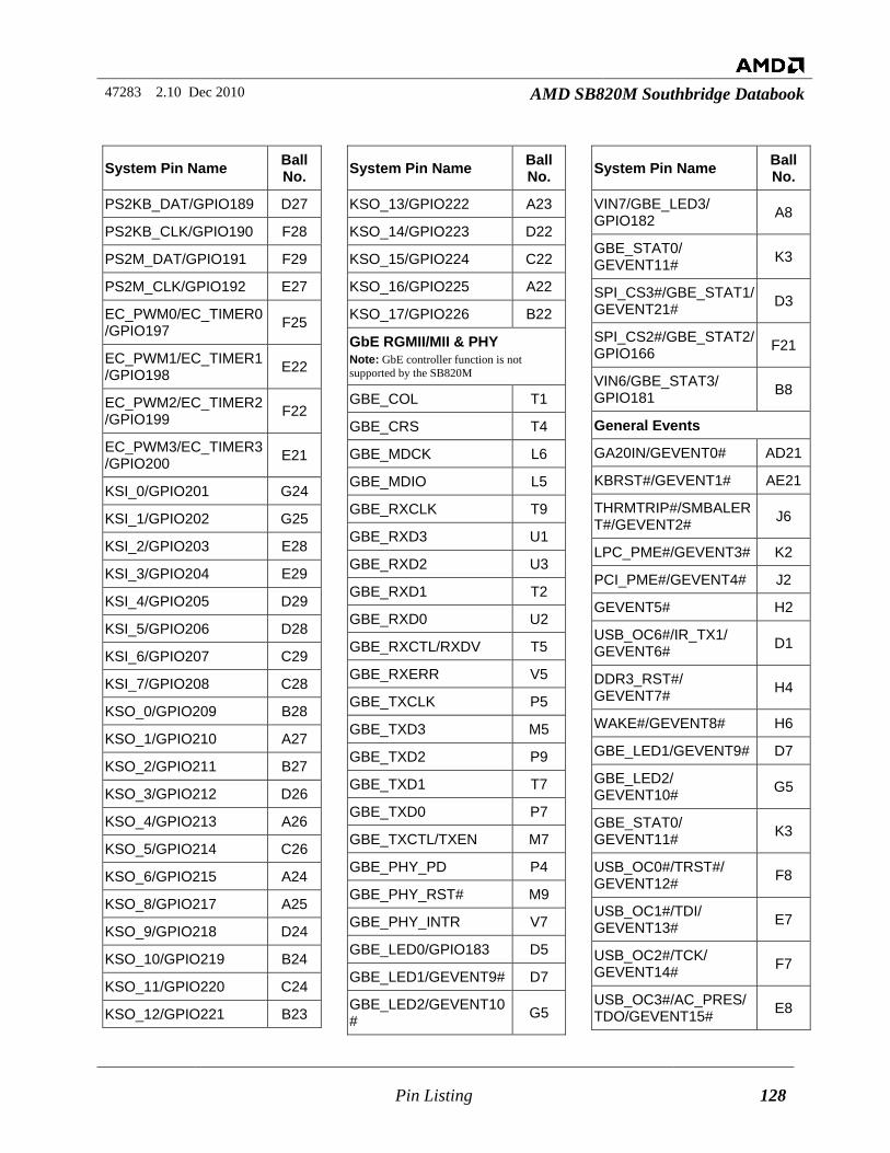
47283 2.10 Dec 2010 AMD SB820M Southbridge Databook
Pin Listing 128
System Pin Name Ball No.
PS2KB_DAT/GPIO189 D27
PS2KB_CLK/GPIO190 F28
PS2M_DAT/GPIO191 F29
PS2M_CLK/GPIO192 E27
EC_PWM0/EC_TIMER0/GPIO197 F25
EC_PWM1/EC_TIMER1/GPIO198 E22
EC_PWM2/EC_TIMER2/GPIO199 F22
EC_PWM3/EC_TIMER3/GPIO200 E21
KSI_0/GPIO201 G24
KSI_1/GPIO202 G25
KSI_2/GPIO203 E28
KSI_3/GPIO204 E29
KSI_4/GPIO205 D29
KSI_5/GPIO206 D28
KSI_6/GPIO207 C29
KSI_7/GPIO208 C28
KSO_0/GPIO209 B28
KSO_1/GPIO210 A27
KSO_2/GPIO211 B27
KSO_3/GPIO212 D26
KSO_4/GPIO213 A26
KSO_5/GPIO214 C26
KSO_6/GPIO215 A24
KSO_8/GPIO217 A25
KSO_9/GPIO218 D24
KSO_10/GPIO219 B24
KSO_11/GPIO220 C24
KSO_12/GPIO221 B23
System Pin Name Ball No.
KSO_13/GPIO222 A23
KSO_14/GPIO223 D22
KSO_15/GPIO224 C22
KSO_16/GPIO225 A22
KSO_17/GPIO226 B22
GbE RGMII/MII & PHY Note: GbE controller function is not supported by the SB820M
GBE_COL T1
GBE_CRS T4
GBE_MDCK L6
GBE_MDIO L5
GBE_RXCLK T9
GBE_RXD3 U1
GBE_RXD2 U3
GBE_RXD1 T2
GBE_RXD0 U2
GBE_RXCTL/RXDV T5
GBE_RXERR V5
GBE_TXCLK P5
GBE_TXD3 M5
GBE_TXD2 P9
GBE_TXD1 T7
GBE_TXD0 P7
GBE_TXCTL/TXEN M7
GBE_PHY_PD P4
GBE_PHY_RST# M9
GBE_PHY_INTR V7
GBE_LED0/GPIO183 D5
GBE_LED1/GEVENT9# D7
GBE_LED2/GEVENT10# G5
System Pin Name Ball No.
VIN7/GBE_LED3/ GPIO182 A8
GBE_STAT0/ GEVENT11# K3
SPI_CS3#/GBE_STAT1/GEVENT21# D3
SPI_CS2#/GBE_STAT2/GPIO166 F21
VIN6/GBE_STAT3/ GPIO181 B8
General Events
GA20IN/GEVENT0# AD21
KBRST#/GEVENT1# AE21
THRMTRIP#/SMBALERT#/GEVENT2# J6
LPC_PME#/GEVENT3# K2
PCI_PME#/GEVENT4# J2
GEVENT5# H2
USB_OC6#/IR_TX1/ GEVENT6# D1
DDR3_RST#/ GEVENT7# H4
WAKE#/GEVENT8# H6
GBE_LED1/GEVENT9# D7
GBE_LED2/ GEVENT10# G5
GBE_STAT0/ GEVENT11# K3
USB_OC0#/TRST#/ GEVENT12# F8
USB_OC1#/TDI/ GEVENT13# E7
USB_OC2#/TCK/ GEVENT14# F7
USB_OC3#/AC_PRES/TDO/GEVENT15# E8
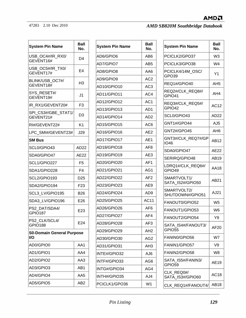
47283 2.10 Dec 2010 AMD SB820M Southbridge Databook
Pin Listing 129
System Pin Name Ball No.
USB_OC4#/IR_RX0/ GEVENT16# D4
USB_OC5#/IR_TX0/ GEVENT17# E4
BLINK/USB_OC7#/ GEVENT18# H3
SYS_RESET#/ GEVENT19# J1
IR_RX1/GEVENT20# F3
SPI_CS3#/GBE_STAT1/GEVENT21# D3
RI#/GEVENT22# K1
LPC_SMI#/GEVENT23# J29
SM Bus
SCL0/GPIO43 AD22
SDA0/GPIO47 AE22
SCL1/GPIO227 F5
SDA1/GPIO228 F4
SCL2/GPIO193 D25
SDA2/GPIO194 F23
SCL3_LV/GPIO195 B26
SDA3_LV/GPIO196 E26
PS2_DAT/SDA4/ GPIO187 E23
PS2_CLK/SCL4/ GPIO188 E24
S0-Domain General Purpose I/O
AD0/GPIO0 AA1
AD1/GPIO1 AA4
AD2/GPIO2 AA3
AD3/GPIO3 AB1
AD4/GPIO4 AA5
AD5/GPIO5 AB2
System Pin Name Ball No.
AD6/GPIO6 AB6
AD7/GPIO7 AB5
AD8/GPIO8 AA6
AD9/GPIO9 AC2
AD10/GPIO10 AC3
AD11/GPIO11 AC4
AD12/GPIO12 AC1
AD13/GPIO13 AD1
AD14/GPIO14 AD2
AD15/GPIO15 AC6
AD16/GPIO16 AE2
AD17/GPIO17 AE1
AD18/GPIO18 AF8
AD19/GPIO19 AE3
AD20/GPIO20 AF1
AD21/GPIO21 AG1
AD22/GPIO22 AF2
AD23/GPIO23 AE9
AD24/GPIO24 AD9
AD25/GPIO25 AC11
AD26/GPIO26 AF6
AD27/GPIO27 AF4
AD28/GPIO28 AF3
AD29/GPIO29 AH2
AD30/GPIO30 AG2
AD31/GPIO31 AH3
INTE#/GPIO32 AJ6
INTF#/GPIO33 AG6
INTG#/GPIO34 AG4
INTH#/GPIO35 AJ4
PCICLK1/GPO36 W1
System Pin Name Ball No.
PCICLK2/GPO37 W3
PCICLK3/GPO38 W4
PCICLK4/14M_OSC/ GPO39 Y1
REQ1#/GPIO40 AH5
REQ2#/CLK_REQ8#/ GPIO41 AH4
REQ3#/CLK_REQ5#/ GPIO42 AC12
SCL0/GPIO43 AD22
GNT1#/GPO44 AJ5
GNT2#/GPO45 AH6
GNT3#/CLK_REQ7#/GPIO46 AB12
SDA0/GPIO47 AE22
SERIRQ/GPIO48 AB19
LDRQ1#/CLK_REQ6#/ GPIO49 AA18
SMARTVOLT1/ SATA_IS2#/GPIO50 AB21
SMARTVOLT2/ SHUTDOWN#/GPIO51 AJ21
FANOUT0/GPIO52 W5
FANOUT1/GPIO53 W6
FANOUT2/GPIO54 Y9
SATA_IS4#/FANOUT3/GPIO55 AF20
FANIN0/GPIO56 W7
FANIN1/GPIO57 V9
FANIN2/GPIO58 W8
SATA_IS5#/FANIN3/ GPIO59 AE19
CLK_REQ0#/ SATA_IS3#/GPIO60 AC18
CLK_REQ1#/FANOUT4/ AB18
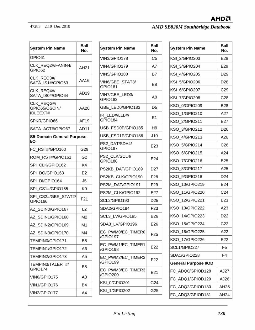
47283 2.10 Dec 2010 AMD SB820M Southbridge Databook
Pin Listing 130
System Pin Name Ball No.
GPIO61
CLK_REQ2#/FANIN4/ GPIO62 AH21
CLK_REQ3#/ SATA_IS1#/GPIO63 AA16
CLK_REQ4#/ SATA_IS0#/GPIO64 AD19
CLK_REQG#/ GPIO65/OSCIN/ IDLEEXT#
AA20
SPKR/GPIO66 AF19
SATA_ACT#/GPIO67 AD11
S5-Domain General Purpose I/O
FC_RST#/GPO160 G29
ROM_RST#/GPIO161 G2
SPI_CLK/GPIO162 K4
SPI_DO/GPIO163 E2
SPI_DI/GPIO164 J5
SPI_CS1#/GPIO165 K9
SPI_CS2#/GBE_STAT2/GPIO166 F21
AZ_SDIN0/GPIO167 L2
AZ_SDIN1/GPIO168 M2
AZ_SDIN2/GPIO169 M1
AZ_SDIN3/GPIO170 M4
TEMPIN0/GPIO171 B6
TEMPIN1/GPIO172 A6
TEMPIN2/GPIO173 A5
TEMPIN3/TALERT#/ GPIO174 B5
VIN0/GPIO175 A3
VIN1/GPIO176 B4
VIN2/GPIO177 A4
System Pin Name Ball No.
VIN3/GPIO178 C5
VIN4/GPIO179 A7
VIN5/GPIO180 B7
VIN6/GBE_STAT3/ GPIO181 B8
VIN7/GBE_LED3/ GPIO182 A8
GBE_LED0/GPIO183 D5
IR_LED#/LLB#/ GPIO184 E1
USB_FSD0P/GPIO185 H9
USB_FSD1P/GPIO186 J10
PS2_DAT/SDA4/ GPIO187 E23
PS2_CLK/SCL4/ GPIO188 E24
PS2KB_DAT/GPIO189 D27
PS2KB_CLK/GPIO190 F28
PS2M_DAT/GPIO191 F29
PS2M_CLK/GPIO192 E27
SCL2/GPIO193 D25
SDA2/GPIO194 F23
SCL3_LV/GPIO195 B26
SDA3_LV/GPIO196 E26
EC_PWM0/EC_TIMER0/GPIO197 F25
EC_PWM1/EC_TIMER1/GPIO198 E22
EC_PWM2/EC_TIMER2/GPIO199 F22
EC_PWM3/EC_TIMER3/GPIO200 E21
KSI_0/GPIO201 G24
KSI_1/GPIO202 G25
System Pin Name Ball No.
KSI_2/GPIO203 E28
KSI_3/GPIO204 E29
KSI_4/GPIO205 D29
KSI_5/GPIO206 D28
KSI_6/GPIO207 C29
KSI_7/GPIO208 C28
KSO_0/GPIO209 B28
KSO_1/GPIO210 A27
KSO_2/GPIO211 B27
KSO_3/GPIO212 D26
KSO_4/GPIO213 A26
KSO_5/GPIO214 C26
KSO_6/GPIO215 A24
KSO_7/GPIO216 B25
KSO_8/GPIO217 A25
KSO_9/GPIO218 D24
KSO_10/GPIO219 B24
KSO_11/GPIO220 C24
KSO_12/GPIO221 B23
KSO_13/GPIO222 A23
KSO_14/GPIO223 D22
KSO_15/GPIO224 C22
KSO_16/GPIO225 A22
KSO_17/GPIO226 B22
SCL1/GPIO227 F5
SDA1/GPIO228 F4
General Purpose I/OD
FC_ADQ0/GPIOD128 AJ27
FC_ADQ1/GPIOD129 AJ26
FC_ADQ2/GPIOD130 AH25
FC_ADQ3/GPIOD131 AH24
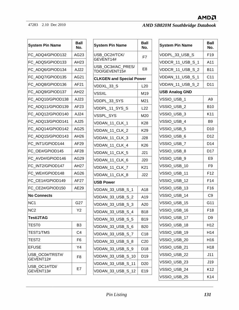
47283 2.10 Dec 2010 AMD SB820M Southbridge Databook
Pin Listing 131
System Pin Name Ball No.
FC_ADQ4/GPIOD132 AG23
FC_ADQ5/GPIOD133 AH23
FC_ADQ6/GPIOD134 AJ22
FC_ADQ7/GPIOD135 AG21
FC_ADQ8/GPIOD136 AF21
FC_ADQ9/GPIOD137 AH22
FC_ADQ10/GPIOD138 AJ23
FC_ADQ11/GPIOD139 AF23
FC_ADQ12/GPIOD140 AJ24
FC_ADQ13/GPIOD141 AJ25
FC_ADQ14/GPIOD142 AG25
FC_ADQ15/GPIOD143 AH26
FC_INT1/GPIOD144 AF29
FC_OE#/GPIOD145 AF28
FC_AVD#/GPIOD146 AG29
FC_INT2/GPIOD147 AH27
FC_WE#/GPIOD148 AG26
FC_CE1#/GPIOD149 AF27
FC_CE2#/GPIOD150 AE29
No Connects
NC1 G27
NC2 Y2
Test/JTAG
TEST0 B3
TEST1/TMS C4
TEST2 F6
EFUSE Y4
USB_OC0#/TRST#/ GEVENT12# F8
USB_OC1#/TDI/ GEVENT13# E7
System Pin Name Ball No.
USB_OC2#/TCK/ GEVENT14# F7
USB_OC3#/AC_PRES/TDO/GEVENT15# E8
CLKGEN and Special Power
VDDXL_33_S L20
VSSXL M19
VDDPL_33_SYS M21
VDDPL_11_SYS_S L22
VSSPL_SYS M20
VDDAN_11_CLK_1 K28
VDDAN_11_CLK_2 K29
VDDAN_11_CLK_3 J28
VDDAN_11_CLK_4 K26
VDDAN_11_CLK_5 J21
VDDAN_11_CLK_6 J20
VDDAN_11_CLK_7 K21
VDDAN_11_CLK_8 J22
USB Power
VDDAN_33_USB_S_1 A18
VDDAN_33_USB_S_2 A19
VDDAN_33_USB_S_3 A20
VDDAN_33_USB_S_4 B18
VDDAN_33_USB_S_5 B19
VDDAN_33_USB_S_6 B20
VDDAN_33_USB_S_7 C18
VDDAN_33_USB_S_8 C20
VDDAN_33_USB_S_9 D18
VDDAN_33_USB_S_10 D19
VDDAN_33_USB_S_11 D20
VDDAN_33_USB_S_12 E19
System Pin Name Ball No.
VDDPL_33_USB_S F19
VDDCR_11_USB_S_1 A11
VDDCR_11_USB_S_2 B11
VDDAN_11_USB_S_1 C11
VDDAN_11_USB_S_2 D11
USB Analog GND
VSSIO_USB_1 A9
VSSIO_USB_2 B10
VSSIO_USB_3 K11
VSSIO_USB_4 B9
VSSIO_USB_5 D10
VSSIO_USB_6 D12
VSSIO_USB_7 D14
VSSIO_USB_8 D17
VSSIO_USB_9 E9
VSSIO_USB_10 F9
VSSIO_USB_11 F12
VSSIO_USB_12 F14
VSSIO_USB_13 F16
VSSIO_USB_14 C9
VSSIO_USB_15 G11
VSSIO_USB_16 F18
VSSIO_USB_17 D9
VSSIO_USB_18 H12
VSSIO_USB_19 H14
VSSIO_USB_20 H16
VSSIO_USB_21 H18
VSSIO_USB_22 J11
VSSIO_USB_23 J19
VSSIO_USB_24 K12
VSSIO_USB_25 K14
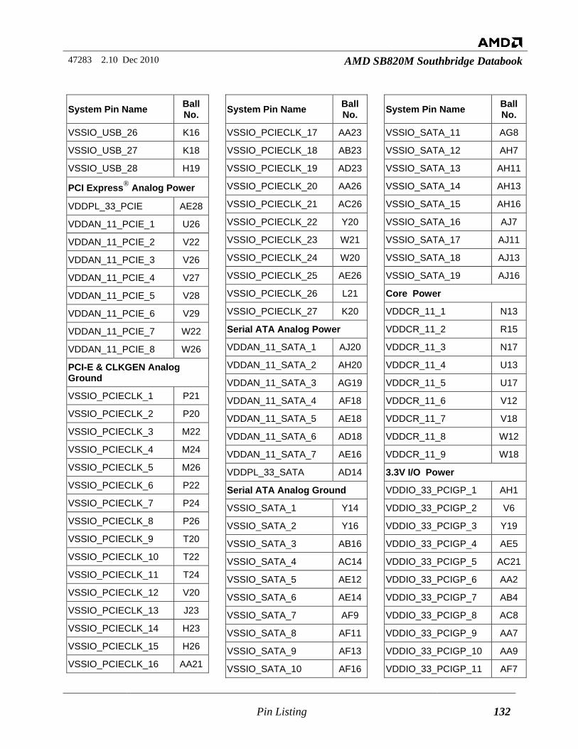
47283 2.10 Dec 2010 AMD SB820M Southbridge Databook
Pin Listing 132
System Pin Name Ball No.
VSSIO_USB_26 K16
VSSIO_USB_27 K18
VSSIO_USB_28 H19
PCI Express® Analog Power
VDDPL_33_PCIE AE28
VDDAN_11_PCIE_1 U26
VDDAN_11_PCIE_2 V22
VDDAN_11_PCIE_3 V26
VDDAN_11_PCIE_4 V27
VDDAN_11_PCIE_5 V28
VDDAN_11_PCIE_6 V29
VDDAN_11_PCIE_7 W22
VDDAN_11_PCIE_8 W26
PCI-E & CLKGEN Analog Ground
VSSIO_PCIECLK_1 P21
VSSIO_PCIECLK_2 P20
VSSIO_PCIECLK_3 M22
VSSIO_PCIECLK_4 M24
VSSIO_PCIECLK_5 M26
VSSIO_PCIECLK_6 P22
VSSIO_PCIECLK_7 P24
VSSIO_PCIECLK_8 P26
VSSIO_PCIECLK_9 T20
VSSIO_PCIECLK_10 T22
VSSIO_PCIECLK_11 T24
VSSIO_PCIECLK_12 V20
VSSIO_PCIECLK_13 J23
VSSIO_PCIECLK_14 H23
VSSIO_PCIECLK_15 H26
VSSIO_PCIECLK_16 AA21
System Pin Name Ball No.
VSSIO_PCIECLK_17 AA23
VSSIO_PCIECLK_18 AB23
VSSIO_PCIECLK_19 AD23
VSSIO_PCIECLK_20 AA26
VSSIO_PCIECLK_21 AC26
VSSIO_PCIECLK_22 Y20
VSSIO_PCIECLK_23 W21
VSSIO_PCIECLK_24 W20
VSSIO_PCIECLK_25 AE26
VSSIO_PCIECLK_26 L21
VSSIO_PCIECLK_27 K20
Serial ATA Analog Power
VDDAN_11_SATA_1 AJ20
VDDAN_11_SATA_2 AH20
VDDAN_11_SATA_3 AG19
VDDAN_11_SATA_4 AF18
VDDAN_11_SATA_5 AE18
VDDAN_11_SATA_6 AD18
VDDAN_11_SATA_7 AE16
VDDPL_33_SATA AD14
Serial ATA Analog Ground
VSSIO_SATA_1 Y14
VSSIO_SATA_2 Y16
VSSIO_SATA_3 AB16
VSSIO_SATA_4 AC14
VSSIO_SATA_5 AE12
VSSIO_SATA_6 AE14
VSSIO_SATA_7 AF9
VSSIO_SATA_8 AF11
VSSIO_SATA_9 AF13
VSSIO_SATA_10 AF16
System Pin Name Ball No.
VSSIO_SATA_11 AG8
VSSIO_SATA_12 AH7
VSSIO_SATA_13 AH11
VSSIO_SATA_14 AH13
VSSIO_SATA_15 AH16
VSSIO_SATA_16 AJ7
VSSIO_SATA_17 AJ11
VSSIO_SATA_18 AJ13
VSSIO_SATA_19 AJ16
Core Power
VDDCR_11_1 N13
VDDCR_11_2 R15
VDDCR_11_3 N17
VDDCR_11_4 U13
VDDCR_11_5 U17
VDDCR_11_6 V12
VDDCR_11_7 V18
VDDCR_11_8 W12
VDDCR_11_9 W18
3.3V I/O Power
VDDIO_33_PCIGP_1 AH1
VDDIO_33_PCIGP_2 V6
VDDIO_33_PCIGP_3 Y19
VDDIO_33_PCIGP_4 AE5
VDDIO_33_PCIGP_5 AC21
VDDIO_33_PCIGP_6 AA2
VDDIO_33_PCIGP_7 AB4
VDDIO_33_PCIGP_8 AC8
VDDIO_33_PCIGP_9 AA7
VDDIO_33_PCIGP_10 AA9
VDDIO_33_PCIGP_11 AF7
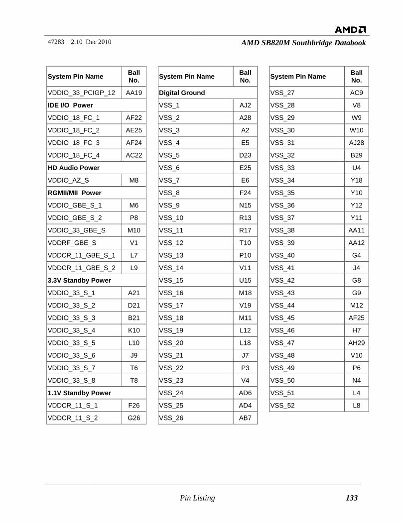
47283 2.10 Dec 2010 AMD SB820M Southbridge Databook
Pin Listing 133
System Pin Name Ball No.
VDDIO_33_PCIGP_12 AA19
IDE I/O Power
VDDIO_18_FC_1 AF22
VDDIO_18_FC_2 AE25
VDDIO_18_FC_3 AF24
VDDIO_18_FC_4 AC22
HD Audio Power
VDDIO_AZ_S M8
RGMII/MII Power
VDDIO_GBE_S_1 M6
VDDIO_GBE_S_2 P8
VDDIO_33_GBE_S M10
VDDRF_GBE_S V1
VDDCR_11_GBE_S_1 L7
VDDCR_11_GBE_S_2 L9
3.3V Standby Power
VDDIO_33_S_1 A21
VDDIO_33_S_2 D21
VDDIO_33_S_3 B21
VDDIO_33_S_4 K10
VDDIO_33_S_5 L10
VDDIO_33_S_6 J9
VDDIO_33_S_7 T6
VDDIO_33_S_8 T8
1.1V Standby Power
VDDCR_11_S_1 F26
VDDCR_11_S_2 G26
System Pin Name Ball No.
Digital Ground
VSS_1 AJ2
VSS_2 A28
VSS_3 A2
VSS_4 E5
VSS_5 D23
VSS_6 E25
VSS_7 E6
VSS_8 F24
VSS_9 N15
VSS_10 R13
VSS_11 R17
VSS_12 T10
VSS_13 P10
VSS_14 V11
VSS_15 U15
VSS_16 M18
VSS_17 V19
VSS_18 M11
VSS_19 L12
VSS_20 L18
VSS_21 J7
VSS_22 P3
VSS_23 V4
VSS_24 AD6
VSS_25 AD4
VSS_26 AB7
System Pin Name Ball No.
VSS_27 AC9
VSS_28 V8
VSS_29 W9
VSS_30 W10
VSS_31 AJ28
VSS_32 B29
VSS_33 U4
VSS_34 Y18
VSS_35 Y10
VSS_36 Y12
VSS_37 Y11
VSS_38 AA11
VSS_39 AA12
VSS_40 G4
VSS_41 J4
VSS_42 G8
VSS_43 G9
VSS_44 M12
VSS_45 AF25
VSS_46 H7
VSS_47 AH29
VSS_48 V10
VSS_49 P6
VSS_50 N4
VSS_51 L4
VSS_52 L8
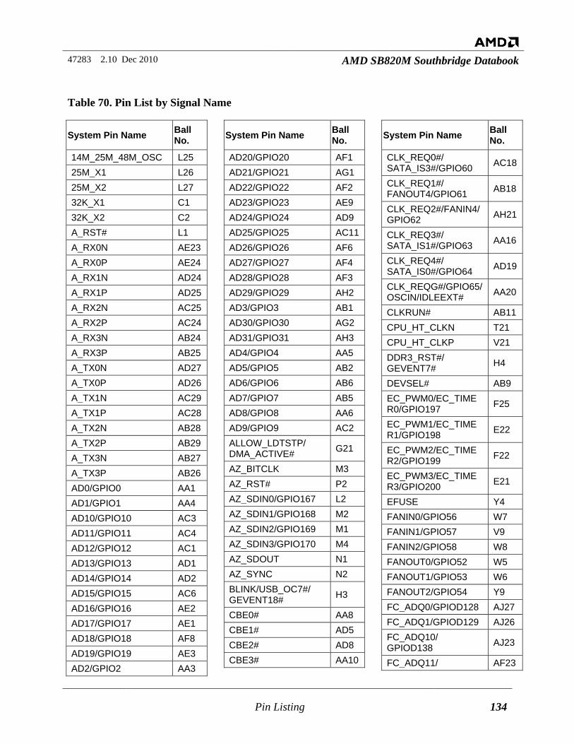
47283 2.10 Dec 2010 AMD SB820M Southbridge Databook
Pin Listing 134
Table 70. Pin List by Signal Name
System Pin Name Ball No.
14M_25M_48M_OSC L25 25M_X1 L26 25M_X2 L27 32K_X1 C1 32K_X2 C2 A_RST# L1 A_RX0N AE23 A_RX0P AE24 A_RX1N AD24 A_RX1P AD25 A_RX2N AC25 A_RX2P AC24 A_RX3N AB24 A_RX3P AB25 A_TX0N AD27 A_TX0P AD26 A_TX1N AC29 A_TX1P AC28 A_TX2N AB28 A_TX2P AB29 A_TX3N AB27 A_TX3P AB26 AD0/GPIO0 AA1 AD1/GPIO1 AA4 AD10/GPIO10 AC3 AD11/GPIO11 AC4 AD12/GPIO12 AC1 AD13/GPIO13 AD1 AD14/GPIO14 AD2 AD15/GPIO15 AC6 AD16/GPIO16 AE2 AD17/GPIO17 AE1 AD18/GPIO18 AF8 AD19/GPIO19 AE3 AD2/GPIO2 AA3
System Pin Name Ball No.
AD20/GPIO20 AF1 AD21/GPIO21 AG1 AD22/GPIO22 AF2 AD23/GPIO23 AE9 AD24/GPIO24 AD9 AD25/GPIO25 AC11 AD26/GPIO26 AF6 AD27/GPIO27 AF4 AD28/GPIO28 AF3 AD29/GPIO29 AH2 AD3/GPIO3 AB1 AD30/GPIO30 AG2 AD31/GPIO31 AH3 AD4/GPIO4 AA5 AD5/GPIO5 AB2 AD6/GPIO6 AB6 AD7/GPIO7 AB5 AD8/GPIO8 AA6 AD9/GPIO9 AC2 ALLOW_LDTSTP/ DMA_ACTIVE# G21
AZ_BITCLK M3 AZ_RST# P2 AZ_SDIN0/GPIO167 L2 AZ_SDIN1/GPIO168 M2 AZ_SDIN2/GPIO169 M1 AZ_SDIN3/GPIO170 M4 AZ_SDOUT N1 AZ_SYNC N2 BLINK/USB_OC7#/ GEVENT18# H3
CBE0# AA8 CBE1# AD5 CBE2# AD8 CBE3# AA10
System Pin Name Ball No.
CLK_REQ0#/ SATA_IS3#/GPIO60 AC18
CLK_REQ1#/ FANOUT4/GPIO61 AB18
CLK_REQ2#/FANIN4/GPIO62 AH21
CLK_REQ3#/ SATA_IS1#/GPIO63 AA16
CLK_REQ4#/ SATA_IS0#/GPIO64 AD19
CLK_REQG#/GPIO65/OSCIN/IDLEEXT# AA20
CLKRUN# AB11 CPU_HT_CLKN T21 CPU_HT_CLKP V21 DDR3_RST#/ GEVENT7# H4
DEVSEL# AB9 EC_PWM0/EC_TIMER0/GPIO197 F25
EC_PWM1/EC_TIMER1/GPIO198 E22
EC_PWM2/EC_TIMER2/GPIO199 F22
EC_PWM3/EC_TIMER3/GPIO200 E21
EFUSE Y4 FANIN0/GPIO56 W7 FANIN1/GPIO57 V9 FANIN2/GPIO58 W8 FANOUT0/GPIO52 W5 FANOUT1/GPIO53 W6 FANOUT2/GPIO54 Y9 FC_ADQ0/GPIOD128 AJ27 FC_ADQ1/GPIOD129 AJ26 FC_ADQ10/ GPIOD138 AJ23
FC_ADQ11/ AF23
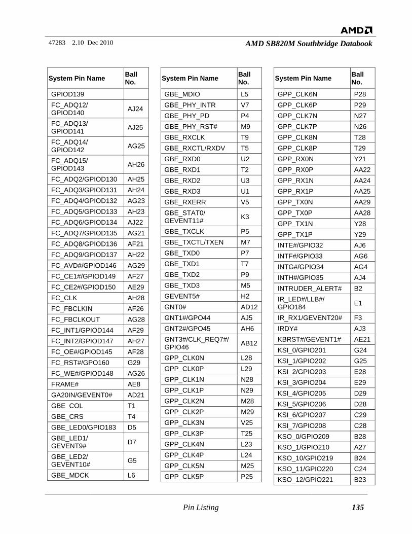
47283 2.10 Dec 2010 AMD SB820M Southbridge Databook
Pin Listing 135
System Pin Name Ball No.
GPIOD139 FC_ADQ12/ GPIOD140 AJ24
FC_ADQ13/ GPIOD141 AJ25
FC_ADQ14/ GPIOD142 AG25
FC_ADQ15/ GPIOD143 AH26
FC_ADQ2/GPIOD130 AH25 FC_ADQ3/GPIOD131 AH24 FC_ADQ4/GPIOD132 AG23 FC_ADQ5/GPIOD133 AH23 FC_ADQ6/GPIOD134 AJ22 FC_ADQ7/GPIOD135 AG21 FC_ADQ8/GPIOD136 AF21 FC_ADQ9/GPIOD137 AH22 FC_AVD#/GPIOD146 AG29 FC_CE1#/GPIOD149 AF27 FC_CE2#/GPIOD150 AE29 FC_CLK AH28 FC_FBCLKIN AF26 FC_FBCLKOUT AG28 FC_INT1/GPIOD144 AF29 FC_INT2/GPIOD147 AH27 FC_OE#/GPIOD145 AF28 FC_RST#/GPO160 G29 FC_WE#/GPIOD148 AG26 FRAME# AE8 GA20IN/GEVENT0# AD21 GBE_COL T1 GBE_CRS T4 GBE_LED0/GPIO183 D5 GBE_LED1/ GEVENT9# D7
GBE_LED2/ GEVENT10# G5
GBE_MDCK L6
System Pin Name Ball No.
GBE_MDIO L5 GBE_PHY_INTR V7 GBE_PHY_PD P4 GBE_PHY_RST# M9 GBE_RXCLK T9 GBE_RXCTL/RXDV T5 GBE_RXD0 U2 GBE_RXD1 T2 GBE_RXD2 U3 GBE_RXD3 U1 GBE_RXERR V5 GBE_STAT0/ GEVENT11# K3
GBE_TXCLK P5 GBE_TXCTL/TXEN M7 GBE_TXD0 P7 GBE_TXD1 T7 GBE_TXD2 P9 GBE_TXD3 M5 GEVENT5# H2 GNT0# AD12 GNT1#/GPO44 AJ5 GNT2#/GPO45 AH6 GNT3#/CLK_REQ7#/GPIO46 AB12
GPP_CLK0N L28 GPP_CLK0P L29 GPP_CLK1N N28 GPP_CLK1P N29 GPP_CLK2N M28 GPP_CLK2P M29 GPP_CLK3N V25 GPP_CLK3P T25 GPP_CLK4N L23 GPP_CLK4P L24 GPP_CLK5N M25 GPP_CLK5P P25
System Pin Name Ball No.
GPP_CLK6N P28 GPP_CLK6P P29 GPP_CLK7N N27 GPP_CLK7P N26 GPP_CLK8N T28 GPP_CLK8P T29 GPP_RX0N Y21 GPP_RX0P AA22 GPP_RX1N AA24 GPP_RX1P AA25 GPP_TX0N AA29 GPP_TX0P AA28 GPP_TX1N Y28 GPP_TX1P Y29 INTE#/GPIO32 AJ6 INTF#/GPIO33 AG6 INTG#/GPIO34 AG4 INTH#/GPIO35 AJ4 INTRUDER_ALERT# B2 IR_LED#/LLB#/ GPIO184 E1
IR_RX1/GEVENT20# F3 IRDY# AJ3 KBRST#/GEVENT1# AE21 KSI_0/GPIO201 G24 KSI_1/GPIO202 G25 KSI_2/GPIO203 E28 KSI_3/GPIO204 E29 KSI_4/GPIO205 D29 KSI_5/GPIO206 D28 KSI_6/GPIO207 C29 KSI_7/GPIO208 C28 KSO_0/GPIO209 B28 KSO_1/GPIO210 A27 KSO_10/GPIO219 B24 KSO_11/GPIO220 C24 KSO_12/GPIO221 B23
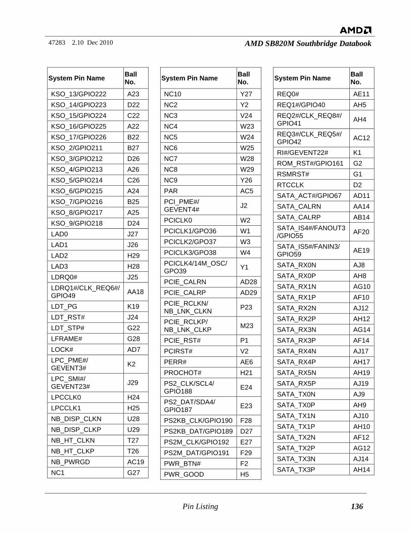
47283 2.10 Dec 2010 AMD SB820M Southbridge Databook
Pin Listing 136
System Pin Name Ball No.
KSO_13/GPIO222 A23 KSO_14/GPIO223 D22 KSO_15/GPIO224 C22 KSO_16/GPIO225 A22 KSO_17/GPIO226 B22 KSO_2/GPIO211 B27 KSO_3/GPIO212 D26 KSO_4/GPIO213 A26 KSO_5/GPIO214 C26 KSO_6/GPIO215 A24 KSO_7/GPIO216 B25 KSO_8/GPIO217 A25 KSO_9/GPIO218 D24 LAD0 J27 LAD1 J26 LAD2 H29 LAD3 H28 LDRQ0# J25 LDRQ1#/CLK_REQ6#/GPIO49 AA18
LDT_PG K19 LDT_RST# J24 LDT_STP# G22 LFRAME# G28 LOCK# AD7 LPC_PME#/ GEVENT3# K2
LPC_SMI#/ GEVENT23# J29
LPCCLK0 H24 LPCCLK1 H25 NB_DISP_CLKN U28 NB_DISP_CLKP U29 NB_HT_CLKN T27 NB_HT_CLKP T26 NB_PWRGD AC19 NC1 G27
System Pin Name Ball No.
NC10 Y27 NC2 Y2 NC3 V24 NC4 W23 NC5 W24 NC6 W25 NC7 W28 NC8 W29 NC9 Y26 PAR AC5 PCI_PME#/ GEVENT4# J2
PCICLK0 W2 PCICLK1/GPO36 W1 PCICLK2/GPO37 W3 PCICLK3/GPO38 W4 PCICLK4/14M_OSC/ GPO39 Y1
PCIE_CALRN AD28 PCIE_CALRP AD29 PCIE_RCLKN/ NB_LNK_CLKN P23
PCIE_RCLKP/ NB_LNK_CLKP M23
PCIE_RST# P1 PCIRST# V2 PERR# AE6 PROCHOT# H21 PS2_CLK/SCL4/ GPIO188 E24
PS2_DAT/SDA4/ GPIO187 E23
PS2KB_CLK/GPIO190 F28 PS2KB_DAT/GPIO189 D27 PS2M_CLK/GPIO192 E27 PS2M_DAT/GPIO191 F29 PWR_BTN# F2 PWR_GOOD H5
System Pin Name Ball No.
REQ0# AE11 REQ1#/GPIO40 AH5 REQ2#/CLK_REQ8#/GPIO41 AH4
REQ3#/CLK_REQ5#/GPIO42 AC12
RI#/GEVENT22# K1 ROM_RST#/GPIO161 G2 RSMRST# G1 RTCCLK D2 SATA_ACT#/GPIO67 AD11 SATA_CALRN AA14 SATA_CALRP AB14 SATA_IS4#/FANOUT3/GPIO55 AF20
SATA_IS5#/FANIN3/ GPIO59 AE19
SATA_RX0N AJ8 SATA_RX0P AH8 SATA_RX1N AG10 SATA_RX1P AF10 SATA_RX2N AJ12 SATA_RX2P AH12 SATA_RX3N AG14 SATA_RX3P AF14 SATA_RX4N AJ17 SATA_RX4P AH17 SATA_RX5N AH19 SATA_RX5P AJ19 SATA_TX0N AJ9 SATA_TX0P AH9 SATA_TX1N AJ10 SATA_TX1P AH10 SATA_TX2N AF12 SATA_TX2P AG12 SATA_TX3N AJ14 SATA_TX3P AH14
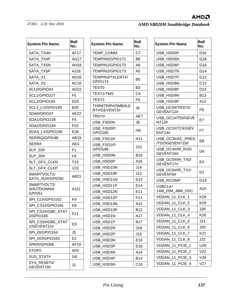
47283 2.10 Dec 2010 AMD SB820M Southbridge Databook
Pin Listing 137
System Pin Name Ball No.
SATA_TX4N AF17 SATA_TX4P AG17 SATA_TX5N AH18 SATA_TX5P AJ18 SATA_X1 AD16 SATA_X2 AC16 SCL0/GPIO43 AD22 SCL1/GPIO227 F5 SCL2/GPIO193 D25 SCL3_LV/GPIO195 B26 SDA0/GPIO47 AE22 SDA1/GPIO228 F4 SDA2/GPIO194 F23 SDA3_LV/GPIO196 E26 SERIRQ/GPIO48 AB19 SERR# AE4 SLP_S3# F1 SLP_S5# H1 SLT_GFX_CLKN T23 SLT_GFX_CLKP V23 SMARTVOLT1/ SATA_IS2#/GPIO50 AB21
SMARTVOLT2/ SHUTDOWN#/ GPIO51
AJ21
SPI_CLK/GPIO162 K4 SPI_CS1#/GPIO165 K9 SPI_CS2#/GBE_STAT2/GPIO166 F21
SPI_CS3#/GBE_STAT1/GEVENT21# D3
SPI_DI/GPIO164 J5 SPI_DO/GPIO163 E2 SPKR/GPIO66 AF19 STOP# AF5 SUS_STAT# G6 SYS_RESET#/ GEVENT19# J1
System Pin Name Ball No.
TEMP_COMM C7 TEMPIN0/GPIO171 B6 TEMPIN1/GPIO172 A6 TEMPIN2/GPIO173 A5 TEMPIN3/TALERT#/ GPIO174 B5
TEST0 B3 TEST1/TMS C4 TEST2 F6 THRMTRIP#/SMBALERT#/GEVENT2# J6
TRDY# AE7 USB_FSD0N J8 USB_FSD0P/ GPIO185 H9
USB_FSD1N H11 USB_FSD1P/ GPIO186 J10
USB_HSD0N B16 USB_HSD0P A16 USB_HSD10N J14 USB_HSD10P J12 USB_HSD11N E12 USB_HSD11P E14 USB_HSD12N E11 USB_HSD12P F11 USB_HSD13N A12 USB_HSD13P B12 USB_HSD1N A17 USB_HSD1P B17 USB_HSD2N J18 USB_HSD2P J16 USB_HSD3N E16 USB_HSD3P E18 USB_HSD4N A14 USB_HSD4P B14 USB_HSD5N C16
System Pin Name Ball No.
USB_HSD5P D16 USB_HSD6N G18 USB_HSD6P G16 USB_HSD7N G14 USB_HSD7P G12 USB_HSD8N C13 USB_HSD8P D13 USB_HSD9N B13 USB_HSD9P A13 USB_OC0#/TRST#/ GEVENT12# F8
USB_OC1#/TDI/GEVENT13# E7
USB_OC2#/TCK/GEVENT14# F7
USB_OC3#/AC_PRES/TDO/GEVENT15# E8
USB_OC4#/IR_RX0/ GEVENT16# D4
USB_OC5#/IR_TX0/ GEVENT17# E4
USB_OC6#/IR_TX1/ GEVENT6# D1
USB_RCOMP G19 USBCLK/ 14M_25M_48M_OSC A10
VDDAN_11_CLK_1 K28 VDDAN_11_CLK_2 K29 VDDAN_11_CLK_3 J28 VDDAN_11_CLK_4 K26 VDDAN_11_CLK_5 J21 VDDAN_11_CLK_6 J20 VDDAN_11_CLK_7 K21 VDDAN_11_CLK_8 J22 VDDAN_11_PCIE_1 U26 VDDAN_11_PCIE_2 V22 VDDAN_11_PCIE_3 V26 VDDAN_11_PCIE_4 V27
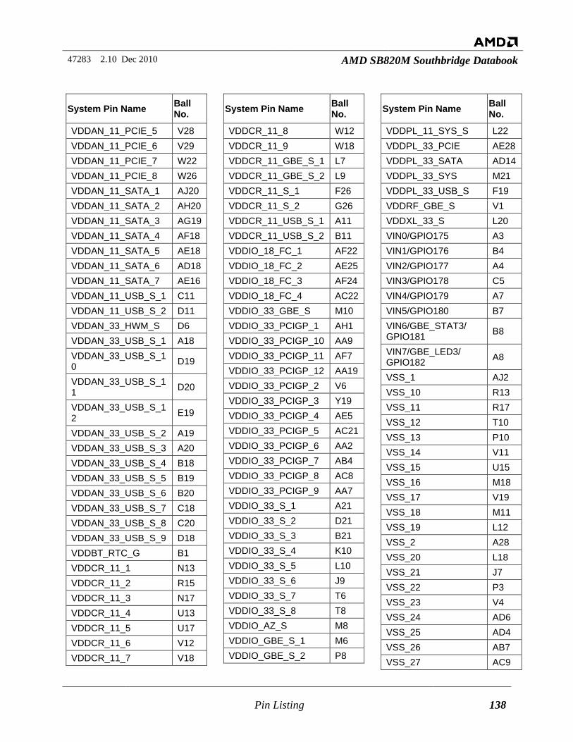
47283 2.10 Dec 2010 AMD SB820M Southbridge Databook
Pin Listing 138
System Pin Name Ball No.
VDDAN_11_PCIE_5 V28 VDDAN_11_PCIE_6 V29 VDDAN_11_PCIE_7 W22 VDDAN_11_PCIE_8 W26 VDDAN_11_SATA_1 AJ20 VDDAN_11_SATA_2 AH20 VDDAN_11_SATA_3 AG19 VDDAN_11_SATA_4 AF18 VDDAN_11_SATA_5 AE18 VDDAN_11_SATA_6 AD18 VDDAN_11_SATA_7 AE16 VDDAN_11_USB_S_1 C11 VDDAN_11_USB_S_2 D11 VDDAN_33_HWM_S D6 VDDAN_33_USB_S_1 A18 VDDAN_33_USB_S_10 D19
VDDAN_33_USB_S_11 D20
VDDAN_33_USB_S_12 E19
VDDAN_33_USB_S_2 A19 VDDAN_33_USB_S_3 A20 VDDAN_33_USB_S_4 B18 VDDAN_33_USB_S_5 B19 VDDAN_33_USB_S_6 B20 VDDAN_33_USB_S_7 C18 VDDAN_33_USB_S_8 C20 VDDAN_33_USB_S_9 D18 VDDBT_RTC_G B1 VDDCR_11_1 N13 VDDCR_11_2 R15 VDDCR_11_3 N17 VDDCR_11_4 U13 VDDCR_11_5 U17 VDDCR_11_6 V12 VDDCR_11_7 V18
System Pin Name Ball No.
VDDCR_11_8 W12 VDDCR_11_9 W18 VDDCR_11_GBE_S_1 L7 VDDCR_11_GBE_S_2 L9 VDDCR_11_S_1 F26 VDDCR_11_S_2 G26 VDDCR_11_USB_S_1 A11 VDDCR_11_USB_S_2 B11 VDDIO_18_FC_1 AF22 VDDIO_18_FC_2 AE25 VDDIO_18_FC_3 AF24 VDDIO_18_FC_4 AC22 VDDIO_33_GBE_S M10 VDDIO_33_PCIGP_1 AH1 VDDIO_33_PCIGP_10 AA9 VDDIO_33_PCIGP_11 AF7 VDDIO_33_PCIGP_12 AA19 VDDIO_33_PCIGP_2 V6 VDDIO_33_PCIGP_3 Y19 VDDIO_33_PCIGP_4 AE5 VDDIO_33_PCIGP_5 AC21 VDDIO_33_PCIGP_6 AA2 VDDIO_33_PCIGP_7 AB4 VDDIO_33_PCIGP_8 AC8 VDDIO_33_PCIGP_9 AA7 VDDIO_33_S_1 A21 VDDIO_33_S_2 D21 VDDIO_33_S_3 B21 VDDIO_33_S_4 K10 VDDIO_33_S_5 L10 VDDIO_33_S_6 J9 VDDIO_33_S_7 T6 VDDIO_33_S_8 T8 VDDIO_AZ_S M8 VDDIO_GBE_S_1 M6 VDDIO_GBE_S_2 P8
System Pin Name Ball No.
VDDPL_11_SYS_S L22 VDDPL_33_PCIE AE28 VDDPL_33_SATA AD14 VDDPL_33_SYS M21 VDDPL_33_USB_S F19 VDDRF_GBE_S V1 VDDXL_33_S L20 VIN0/GPIO175 A3 VIN1/GPIO176 B4 VIN2/GPIO177 A4 VIN3/GPIO178 C5 VIN4/GPIO179 A7 VIN5/GPIO180 B7 VIN6/GBE_STAT3/ GPIO181 B8
VIN7/GBE_LED3/ GPIO182 A8
VSS_1 AJ2 VSS_10 R13 VSS_11 R17 VSS_12 T10 VSS_13 P10 VSS_14 V11 VSS_15 U15 VSS_16 M18 VSS_17 V19 VSS_18 M11 VSS_19 L12 VSS_2 A28 VSS_20 L18 VSS_21 J7 VSS_22 P3 VSS_23 V4 VSS_24 AD6 VSS_25 AD4 VSS_26 AB7 VSS_27 AC9
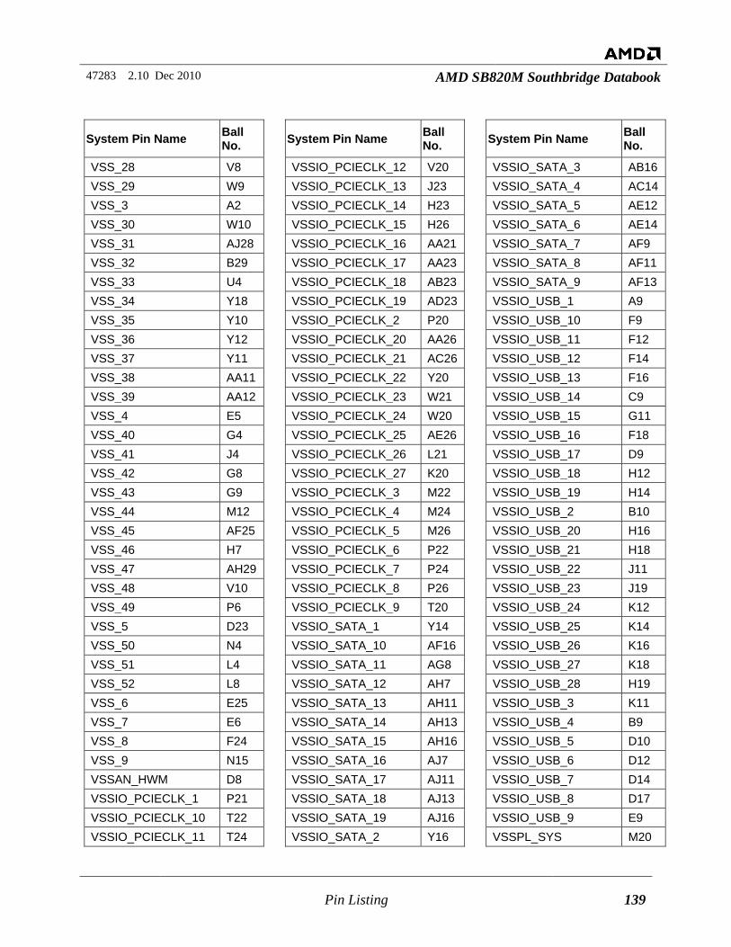
47283 2.10 Dec 2010 AMD SB820M Southbridge Databook
Pin Listing 139
System Pin Name Ball No.
VSS_28 V8 VSS_29 W9 VSS_3 A2 VSS_30 W10 VSS_31 AJ28 VSS_32 B29 VSS_33 U4 VSS_34 Y18 VSS_35 Y10 VSS_36 Y12 VSS_37 Y11 VSS_38 AA11 VSS_39 AA12 VSS_4 E5 VSS_40 G4 VSS_41 J4 VSS_42 G8 VSS_43 G9 VSS_44 M12 VSS_45 AF25 VSS_46 H7 VSS_47 AH29 VSS_48 V10 VSS_49 P6 VSS_5 D23 VSS_50 N4 VSS_51 L4 VSS_52 L8 VSS_6 E25 VSS_7 E6 VSS_8 F24 VSS_9 N15 VSSAN_HWM D8 VSSIO_PCIECLK_1 P21 VSSIO_PCIECLK_10 T22 VSSIO_PCIECLK_11 T24
System Pin Name Ball No.
VSSIO_PCIECLK_12 V20 VSSIO_PCIECLK_13 J23 VSSIO_PCIECLK_14 H23 VSSIO_PCIECLK_15 H26 VSSIO_PCIECLK_16 AA21 VSSIO_PCIECLK_17 AA23 VSSIO_PCIECLK_18 AB23 VSSIO_PCIECLK_19 AD23 VSSIO_PCIECLK_2 P20 VSSIO_PCIECLK_20 AA26 VSSIO_PCIECLK_21 AC26 VSSIO_PCIECLK_22 Y20 VSSIO_PCIECLK_23 W21 VSSIO_PCIECLK_24 W20 VSSIO_PCIECLK_25 AE26 VSSIO_PCIECLK_26 L21 VSSIO_PCIECLK_27 K20 VSSIO_PCIECLK_3 M22 VSSIO_PCIECLK_4 M24 VSSIO_PCIECLK_5 M26 VSSIO_PCIECLK_6 P22 VSSIO_PCIECLK_7 P24 VSSIO_PCIECLK_8 P26 VSSIO_PCIECLK_9 T20 VSSIO_SATA_1 Y14 VSSIO_SATA_10 AF16 VSSIO_SATA_11 AG8 VSSIO_SATA_12 AH7 VSSIO_SATA_13 AH11 VSSIO_SATA_14 AH13 VSSIO_SATA_15 AH16 VSSIO_SATA_16 AJ7 VSSIO_SATA_17 AJ11 VSSIO_SATA_18 AJ13 VSSIO_SATA_19 AJ16 VSSIO_SATA_2 Y16
System Pin Name Ball No.
VSSIO_SATA_3 AB16 VSSIO_SATA_4 AC14 VSSIO_SATA_5 AE12 VSSIO_SATA_6 AE14 VSSIO_SATA_7 AF9 VSSIO_SATA_8 AF11 VSSIO_SATA_9 AF13 VSSIO_USB_1 A9 VSSIO_USB_10 F9 VSSIO_USB_11 F12 VSSIO_USB_12 F14 VSSIO_USB_13 F16 VSSIO_USB_14 C9 VSSIO_USB_15 G11 VSSIO_USB_16 F18 VSSIO_USB_17 D9 VSSIO_USB_18 H12 VSSIO_USB_19 H14 VSSIO_USB_2 B10 VSSIO_USB_20 H16 VSSIO_USB_21 H18 VSSIO_USB_22 J11 VSSIO_USB_23 J19 VSSIO_USB_24 K12 VSSIO_USB_25 K14 VSSIO_USB_26 K16 VSSIO_USB_27 K18 VSSIO_USB_28 H19 VSSIO_USB_3 K11 VSSIO_USB_4 B9 VSSIO_USB_5 D10 VSSIO_USB_6 D12 VSSIO_USB_7 D14 VSSIO_USB_8 D17 VSSIO_USB_9 E9 VSSPL_SYS M20
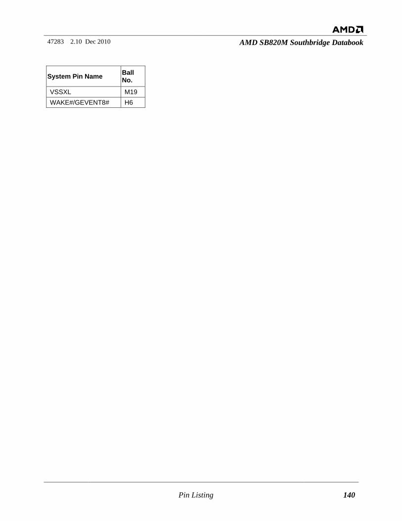
47283 2.10 Dec 2010 AMD SB820M Southbridge Databook
Pin Listing 140
System Pin Name Ball No.
VSSXL M19 WAKE#/GEVENT8# H6
47283 2.10 Dec 2010 AMD SB820M Southbridge Databook
Pin Listing 141