Embed Size (px)
Citation preview

AMD SB700/710/750 Register Programming Requirements
Technical Reference Manual Rev. 2.08
P/N: 42413_sb7xx_rpr_nda_2.08
© 2009 Advanced Micro Devices, Inc.
. Trademarks AMD, the AMD Arrow logo, Athlon, and combinations thereof, ATI, ATI logo, Radeon, and Crossfire are trademarks of Advanced Micro Devices, Inc.
HyperTransport is a licensed trademark of the HyperTransport Technology Consortium.
Microsoft and Windows are registered trademarks of Microsoft Corporation.
Other product names used in this publication are for identification purposes only and may be trademarks of their respective companies.
Disclaimer
The contents of this document are provided in connection with Advanced Micro Devices, Inc. ("AMD") products. AMD makes no representations or warranties with respect to the accuracy or completeness of the contents of this publication and reserves the right to make changes to specifications and product descriptions at any time without notice. No license, whether express, implied, arising by estoppel, or otherwise, to any intellectual property rights are granted by this publication. Except as set forth in AMD's Standard Terms and Conditions of Sale, AMD assumes no liability whatsoever, and disclaims any express or implied warranty, relating to its products including, but not limited to, the implied warranty of merchantability, fitness for a particular purpose, or infringement of any intellectual property right.
AMD's products are not designed, intended, authorized or warranted for use as components in systems intended for surgical implant into the body, or in other applications intended to support or sustain life, or in any other application in which the failure of AMD's product could create a situation where personal injury, death, or severe property or environmental damage may occur. AMD reserves the right to discontinue or make changes to its products at any time without notice.
© 2009 Advanced Micro Devices, Inc. TOC AMD SB700/710/750 Register Programming Requirements Page 3
Table of Contents
1 Introduction ................................................................................................................ 7 1.1 About This Manual........................................................................................................................ 7 1.2 AMD SB700 Block Diagram ........................................................................................................ 8 1.3 Register Reference Information .................................................................................................... 9
2 ACPI/SMBUS Controller (bus-0, dev-20, fun-0)................................................ 10 2.1 Enabling Legacy Interrupt........................................................................................................... 10 2.2 Unblocked SMI Command Port .................................................................................................. 10 2.3 WakeIO Base Address ................................................................................................................ 10 2.4 C-State and VID/FID Change ..................................................................................................... 10 2.5 Enabling Non-Posted Memory Write.......................................................................................... 13 2.6 Therm Trip Settings .................................................................................................................... 13 2.7 Sx State Settings.......................................................................................................................... 13 2.8 Output Drive Strength Settings ................................................................................................... 14 2.9 SUS_STAT# Enhancement......................................................................................................... 14 2.10 Interrupt Routing/Filtering .......................................................................................................... 14 2.11 IO Trap Settings .......................................................................................................................... 15 2.12 Enabling ACPI Registers ............................................................................................................ 15 2.13 Legacy DMA Prefetch Enhancement.......................................................................................... 16 2.14 USB Set BM_STS....................................................................................................................... 16 2.15 Enabling Spread Spectrum .......................................................................................................... 16 2.16 PCIE Native Mode ...................................................................................................................... 17 2.17 Hardware Monitor ....................................................................................................................... 17 2.18 Cir Interrupt Config..................................................................................................................... 18 2.19 SMBUS Pci Config ..................................................................................................................... 18 2.20 IMC Access Control.................................................................................................................... 18 2.21 CPU Reset ................................................................................................................................... 19 2.22 Disabling Legacy USB Fast SMI# .............................................................................................. 19 2.23 ASF Programming Sequence ...................................................................................................... 19 2.24 ASF SMBUS Programming Sequence........................................................................................ 22 2.25 ASF Listen Mode Programming Sequence ................................................................................. 24 2.26 ACPI System Clock Setting ........................................................................................................ 27 2.27 Integrated Pull-up and Pull-down Settings.................................................................................. 27 2.28 Revision ID ................................................................................................................................. 27 2.29 Alternate Pin for 14 MHz Clock input ........................................................................................ 28 2.30 Gevent5 as GPIO......................................................................................................................... 28 2.31 PM_TURN_OFF_MSG during ASF Shutdown ......................................................................... 29 2.32 SMBUS Block Write Filtering .................................................................................................... 29 2.33 SMBUS Write Sequence ............................................................................................................. 29
3 LPC Controller (bus-0, dev-20, fun-3)................................................................. 31 3.1 IO / Mem Decoding..................................................................................................................... 31
© 2009 Advanced Micro Devices, Inc. TOC AMD SB700/710/750 Register Programming Requirements Page 4
3.2 SPI Bus........................................................................................................................................ 31
4 A-Link Express Settings - Indirect I/O Access................................................. 32 4.1 Defining AB_REG_BAR............................................................................................................ 32 4.2 Clearing AB_INDX..................................................................................................................... 32 4.3 Enabling Upstream DMA Access ............................................................................................... 33 4.4 IDE/PCIB Prefetch Settings ........................................................................................................ 33 4.5 OHCI Prefetch Settings............................................................................................................... 33 4.6 B-Link Client’s Credit Variable Settings for the Downstream Arbitration Equation ................. 34 4.7 Enabling Additional Address Bits Checking in Downstream Register Programming ................ 34 4.8 Set B-Link Prefetch Mode........................................................................................................... 34 4.9 Enabling Detection of Upstream Interrupts................................................................................. 35 4.10 Enabling Downstream Posted Transactions to Pass Non-Posted Transactions........................... 35 4.11 Programming Cycle Delay for AB and BIF Clock Gating.......................................................... 35 4.12 Enabling AB and BIF Clock Gating............................................................................................ 36 4.13 Enabling AB Int_Arbiter Enhancement ...................................................................................... 36 4.14 Enabling Requester ID ................................................................................................................ 36 4.15 Selecting the LPC FRAME# Assertion Timing on Power-up..................................................... 36 4.16 SMI IO Write .............................................................................................................................. 37
5 PCIB (PCI-bridge, bus-0, dev-20, fun-04)........................................................... 38 5.1 Enabling PCI-bridge Subtractive Decode ................................................................................... 38 5.2 PCI-bridge Upstream Dual Address Window ............................................................................. 38 5.3 PCI Bus 64-byte DMA Read Access .......................................................................................... 38 5.4 PCI Bus DMA Write Cacheline Alignment ................................................................................ 39 5.5 Master Latency Timer ................................................................................................................. 39 5.6 DMA Read Command Match...................................................................................................... 39 5.7 Enabling Idle To GNT# Check ................................................................................................... 40 5.8 GNT# Timing Adjustment .......................................................................................................... 40 5.9 Enabling Fast Back to Back Retry .............................................................................................. 40 5.10 Enabling Lock Operation ............................................................................................................ 40 5.11 Enabling Additional Optional PCI Clock (PCICLK5)................................................................ 41 5.12 Enabling One-Prefetch-Channel Mode ....................................................................................... 41 5.13 Disabling PCIB MSI Capability.................................................................................................. 41 5.14 Adjusting CLKRUN#.................................................................................................................. 42
6 USB – OHCI & EHCI Controllers (bus-0, dev-18/19, fun-00 ~02/ bus-0, dev-20, fun-05)........................................................................................................................ 43
6.1 Enabling/Disabling OHCI and EHCI Controllers ....................................................................... 43 6.2 USB Device Support to Wake Up System from S3/S4 State ...................................................... 44 6.3 USB S4/S5 Wakeup or PHY Power Down Support ................................................................... 44 6.4 USB PHY Auto Calibration Setting............................................................................................ 44 6.5 USB Reset Sequence................................................................................................................... 44 6.6 USB Advanced Sleep Control..................................................................................................... 45
© 2009 Advanced Micro Devices, Inc. TOC AMD SB700/710/750 Register Programming Requirements Page 5
6.7 USB 48 MHz Clock Source Settings .......................................................................................... 45 6.8 Adjusting USB 2.0 Ports Driving Strength ................................................................................. 45 6.9 In and Out Data Packet FIFO Threshold..................................................................................... 46 6.10 OHCI MSI Function Setting ....................................................................................................... 46 6.11 EHCI Advance Asynchronous Enhancement.............................................................................. 47 6.12 EHCI Advance PHY Power Savings........................................................................................... 47 6.13 Enabling Fix for EHCI Controller Driver Yellow Sign Issue ..................................................... 47 6.14 Enabling Fix to Cover the Corner Case S3 Wake Up Issue ........................................................ 48 6.15 EHCI Async Park Mode.............................................................................................................. 48 6.16 MSI Feature in USB 2.0 Controller............................................................................................. 49 6.17 EHCI Dynamic Clock Gating Feature......................................................................................... 49
6.17.1 Sample Code for the Workaround Described in SB7xx Erratum #11 (ERN # ERA12011) ................49 6.18 USB 1.1 ISO OUT Devices/Speaker Noise ................................................................................ 52 6.19 USB Controller DMA Read Delay Tolerant. .............................................................................. 52 6.20 Async Park Mode ........................................................................................................................ 52 6.21 Resume Reset Timing ................................................................................................................. 53 6.22 Advance Async Enhancement..................................................................................................... 54 6.23 USB Periodic Cache Setting ....................................................................................................... 54
7 SATA: Dev-17, Func-0 ............................................................................................ 55 7.1 Enabling SATA........................................................................................................................... 55 7.2 SATA Initialization ..................................................................................................................... 55 7.3 Disabling SATA.......................................................................................................................... 56 7.4 SATA Power Saving ................................................................................................................... 57 7.5 Disabling Unused SATA Ports.................................................................................................... 57 7.6 SATA Subclass Programming Sequence .................................................................................... 58 7.7 SATA PHY Programming Sequence .......................................................................................... 59 7.8 SATA Identification Programming Sequence for IDE Mode ..................................................... 60
7.8.1 SATA Drive Detection ........................................................................................................................60 7.9 Restoring SATA Registers after S3 Resume State...................................................................... 61 7.10 External SATA Ports Indication Registers.................................................................................. 62 7.11 Aggressive Link Power Management ......................................................................................... 63 7.12 SATA MSI Capability................................................................................................................. 63 7.13 Flash Controller........................................................................................................................... 64
7.13.1 Enabling Flash Controller ....................................................................................................................64 7.13.2 Config SATA BAR2 for Flash Controller ...........................................................................................64 7.13.3 FcForceHoldRstEn ..............................................................................................................................64 7.13.4 HcCrcEn ..............................................................................................................................................64 7.13.5 Error Mode...........................................................................................................................................65 7.13.6 PinConfig.............................................................................................................................................65 7.13.7 TachMode............................................................................................................................................65 7.13.8 TcaMode..............................................................................................................................................65 7.13.9 NumBankMode....................................................................................................................................66 7.13.10 FC CLK Program .......................................................................................................................66 7.13.11 SlpStateForceRstEn....................................................................................................................66
7.14 Restoring FC Registers After S3 Resume State .......................................................................... 66
© 2009 Advanced Micro Devices, Inc. TOC AMD SB700/710/750 Register Programming Requirements Page 6
7.15 Disabling CCC (Command Completion Coalescing) Support .................................................... 67
8 LPC (bus-0, dev-20, fun-03) .................................................................................. 68 8.1 Enabling/Disabling LPC Controller ............................................................................................ 68 8.2 Parallel Port ECP Mode Support................................................................................................. 68
9 IDE Controller (bus-0, dev-20, fun-01) .............................................................. 69 9.1 Disabling IDE MSI Capability .................................................................................................... 69 9.2 Enabling IDE Data Bus DD7 Pull-Down Resistor...................................................................... 69
10 Embedded Controller (EC).................................................................................... 70 10.1 Enable Using SAEN in Keyboard Controller.............................................................................. 70 10.2 GA20 Polarity ............................................................................................................................. 70 10.3 Re-alignment of EC 33Mhz Clock.............................................................................................. 70 10.4 Monitoring PwrGood on Sleep Detection ................................................................................... 71 10.5 Clearing start_carrier in IR after Learning Mode is Complete.................................................... 71 10.6 Enabling Power Saving on LPC Clock in S5 .............................................................................. 71 10.7 Supporting Open Drain on pad ps2_dat ...................................................................................... 72 10.8 Enabling Edge-triggering of CIR Interrupt to ACPI ................................................................... 72 10.9 Disabling Pull-ups and Pull-downs in Pads EcGpio4/5 .............................................................. 72 10.10 Disabling Pull-ups and Pull-downs in Pads EcGpio6/7 ........................................................ 73 10.11 Disabling Pull-ups and Pull-downs in Pads EcGpio0/1 ........................................................ 73 10.12 EC Enhanced Mode - PMIO ................................................................................................. 73 10.13 EC Enhanced Mode - SM PCI .............................................................................................. 74 10.14 EC Enhanced Mode - LPC.................................................................................................... 75
11 HD Audio (bus-0, dev-20, fun-02) ........................................................................ 76 11.1 Enabling/Disabling HD Audio .................................................................................................... 76 11.2 HD Audio Interrupt Routing Table ............................................................................................. 76 11.3 Audio Port Configuration............................................................................................................ 76
Appendix: Revision History ....................................................................................... 78
© 2009 Advanced Micro Devices, Inc. Introduction AMD SB700/710/750 Register Programming Requirements Page 7
1 Introduction
1.1 About This Manual
This document lists the register settings required for the proper operation of the AMD SB700/710/750 (referred to collectively as “SB7x0” in this document). Most of the register settings are mandatory and should be implemented as described in this document. The document will be updated periodically with new or revised settings that are determined during the qualification of the SB7x0. Please refer to the latest updated document on the ORC.
This document should be used in conjunction with the related AMD SB700/710/50 BIOS Developer’s Guide and the AMD SB700/710/750 Register Reference Guide.
Note: In this document, changes/additions from the previous release are highlighted in red. Refer to the Appendix: Revision History at the end of this document for a detailed revision history.
© 2009 Advanced Micro Devices, Inc. Introduction AMD SB700/710/750 Register Programming Requirements Page 8
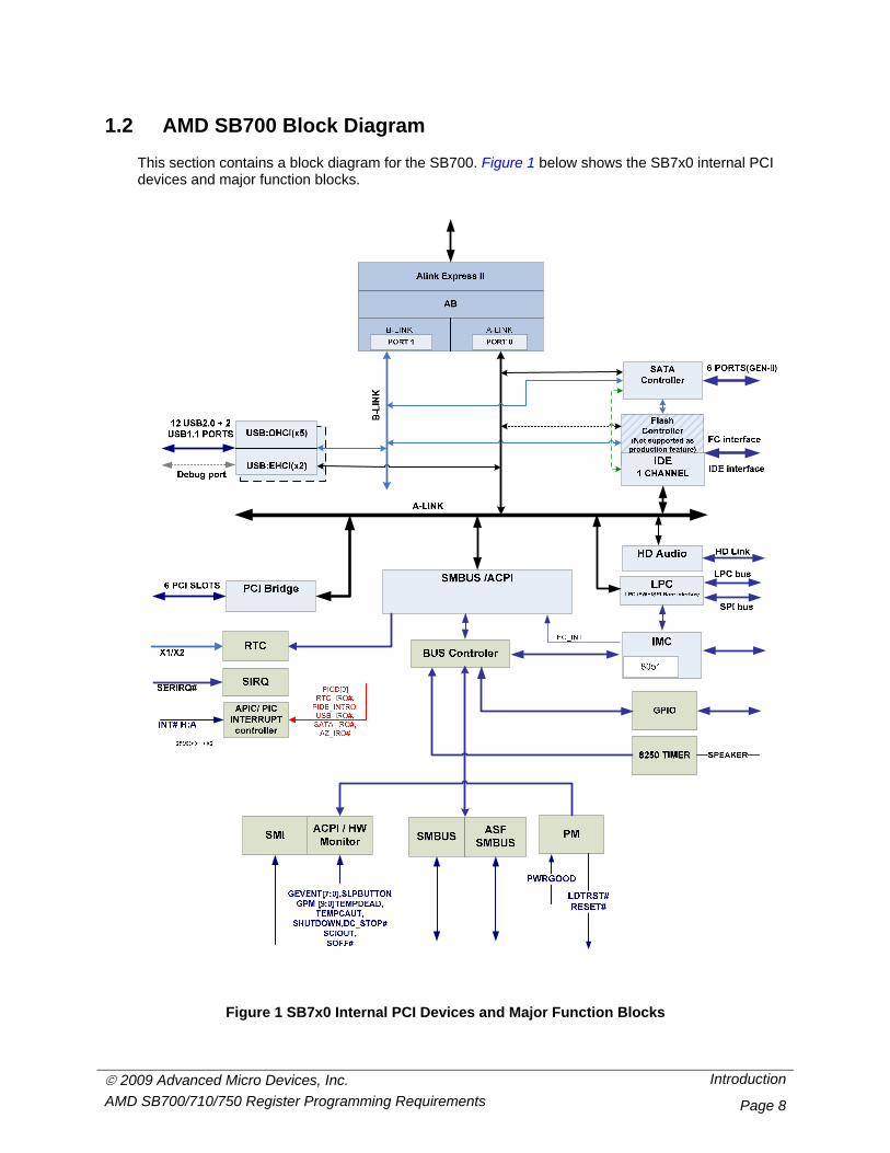
1.2 AMD SB700 Block Diagram
This section contains a block diagram for the SB700. Figure 1 below shows the SB7x0 internal PCI devices and major function blocks.
Figure 1 SB7x0 Internal PCI Devices and Major Function Blocks
© 2009 Advanced Micro Devices, Inc. Introduction AMD SB700/710/750 Register Programming Requirements Page 9
1.3 Register Reference Information
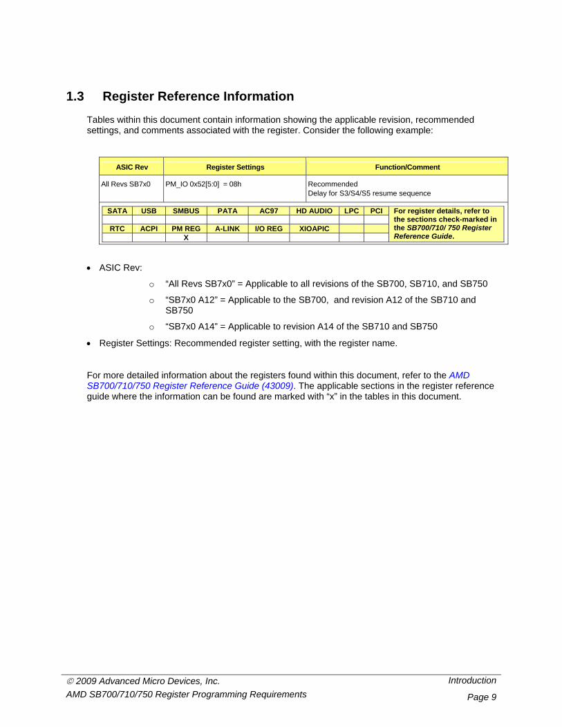
Tables within this document contain information showing the applicable revision, recommended settings, and comments associated with the register. Consider the following example:
ASIC Rev Register Settings Function/Comment
All Revs SB7x0 PM_IO 0x52[5:0] = 08h Recommended Delay for S3/S4/S5 resume sequence
SATA USB SMBUS PATA AC97 HD AUDIO LPC PCI
RTC ACPI PM REG A-LINK I/O REG XIOAPIC X
For register details, refer to the sections check-marked in the SB700/710/ 750 Register Reference Guide.
• ASIC Rev:
o “All Revs SB7x0” = Applicable to all revisions of the SB700, SB710, and SB750
o “SB7x0 A12” = Applicable to the SB700, and revision A12 of the SB710 and SB750
o “SB7x0 A14” = Applicable to revision A14 of the SB710 and SB750
• Register Settings: Recommended register setting, with the register name.
For more detailed information about the registers found within this document, refer to the AMD SB700/710/750 Register Reference Guide (43009). The applicable sections in the register reference guide where the information can be found are marked with “x” in the tables in this document.
© 2009 Advanced Micro Devices, Inc. ACPI/SMBUS Controller (bus-0, dev-20, fun-0) AMD SB700/710/750 Register Programming Requirements Page 10
2 ACPI/SMBUS Controller (bus-0, dev-20, fun-0)
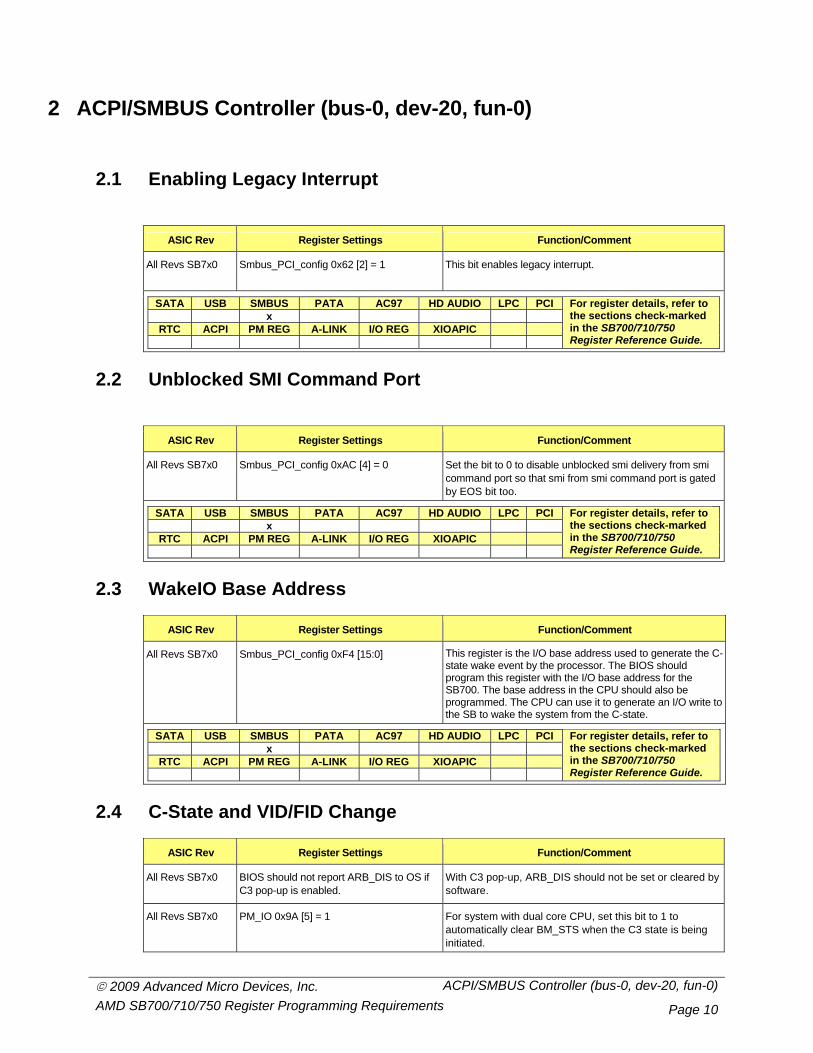
2.1 Enabling Legacy Interrupt
ASIC Rev Register Settings Function/Comment
All Revs SB7x0 Smbus_PCI_config 0x62 [2] = 1 This bit enables legacy interrupt.
SATA USB SMBUS PATA AC97 HD AUDIO LPC PCI x
RTC ACPI PM REG A-LINK I/O REG XIOAPIC
For register details, refer to the sections check-marked in the SB700/710/750 Register Reference Guide.
2.2 Unblocked SMI Command Port
ASIC Rev Register Settings Function/Comment
All Revs SB7x0 Smbus_PCI_config 0xAC [4] = 0 Set the bit to 0 to disable unblocked smi delivery from smi command port so that smi from smi command port is gated by EOS bit too.
SATA USB SMBUS PATA AC97 HD AUDIO LPC PCI x
RTC ACPI PM REG A-LINK I/O REG XIOAPIC
For register details, refer to the sections check-marked in the SB700/710/750 Register Reference Guide.
2.3 WakeIO Base Address
ASIC Rev Register Settings Function/Comment
All Revs SB7x0 Smbus_PCI_config 0xF4 [15:0] This register is the I/O base address used to generate the C-state wake event by the processor. The BIOS should program this register with the I/O base address for the SB700. The base address in the CPU should also be programmed. The CPU can use it to generate an I/O write to the SB to wake the system from the C-state.
SATA USB SMBUS PATA AC97 HD AUDIO LPC PCI x
RTC ACPI PM REG A-LINK I/O REG XIOAPIC
For register details, refer to the sections check-marked in the SB700/710/750 Register Reference Guide.
2.4 C-State and VID/FID Change
ASIC Rev Register Settings Function/Comment
All Revs SB7x0 BIOS should not report ARB_DIS to OS if C3 pop-up is enabled.
With C3 pop-up, ARB_DIS should not be set or cleared by software.
All Revs SB7x0 PM_IO 0x9A [5] = 1 For system with dual core CPU, set this bit to 1 to automatically clear BM_STS when the C3 state is being initiated.
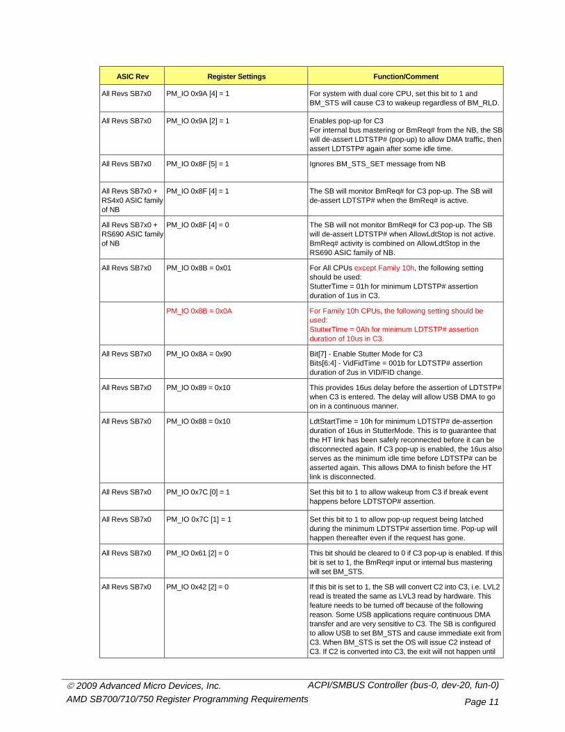
© 2009 Advanced Micro Devices, Inc. ACPI/SMBUS Controller (bus-0, dev-20, fun-0) AMD SB700/710/750 Register Programming Requirements Page 11
ASIC Rev Register Settings Function/Comment
All Revs SB7x0 PM_IO 0x9A [4] = 1 For system with dual core CPU, set this bit to 1 and BM_STS will cause C3 to wakeup regardless of BM_RLD.
All Revs SB7x0 PM_IO 0x9A [2] = 1 Enables pop-up for C3 For internal bus mastering or BmReq# from the NB, the SB will de-assert LDTSTP# (pop-up) to allow DMA traffic, then assert LDTSTP# again after some idle time.
All Revs SB7x0 PM_IO 0x8F [5] = 1 Ignores BM_STS_SET message from NB
All Revs SB7x0 + RS4x0 ASIC family of NB
PM_IO 0x8F [4] = 1 The SB will monitor BmReq# for C3 pop-up. The SB will de-assert LDTSTP# when the BmReq# is active.
All Revs SB7x0 + RS690 ASIC family of NB
PM_IO 0x8F [4] = 0 The SB will not monitor BmReq# for C3 pop-up. The SB will de-assert LDTSTP# when AllowLdtStop is not active. BmReq# activity is combined on AllowLdtStop in the RS690 ASIC family of NB.
All Revs SB7x0 PM_IO 0x8B = 0x01 For All CPUs except Family 10h, the following setting should be used: StutterTime = 01h for minimum LDTSTP# assertion duration of 1us in C3.
PM_IO 0x8B = 0x0A For Family 10h CPUs, the following setting should be used: StutterTime = 0Ah for minimum LDTSTP# assertion duration of 10us in C3.
All Revs SB7x0 PM_IO 0x8A = 0x90 Bit[7] - Enable Stutter Mode for C3 Bits[6:4] - VidFidTime = 001b for LDTSTP# assertion duration of 2us in VID/FID change.
All Revs SB7x0 PM_IO 0x89 = 0x10 This provides 16us delay before the assertion of LDTSTP# when C3 is entered. The delay will allow USB DMA to go on in a continuous manner.
All Revs SB7x0 PM_IO 0x88 = 0x10 LdtStartTime = 10h for minimum LDTSTP# de-assertion duration of 16us in StutterMode. This is to guarantee that the HT link has been safely reconnected before it can be disconnected again. If C3 pop-up is enabled, the 16us also serves as the minimum idle time before LDTSTP# can be asserted again. This allows DMA to finish before the HT link is disconnected.
All Revs SB7x0 PM_IO 0x7C [0] = 1 Set this bit to 1 to allow wakeup from C3 if break event happens before LDTSTOP# assertion.
All Revs SB7x0 PM_IO 0x7C [1] = 1
Set this bit to 1 to allow pop-up request being latched during the minimum LDTSTP# assertion time. Pop-up will happen thereafter even if the request has gone.
All Revs SB7x0 PM_IO 0x61 [2] = 0 This bit should be cleared to 0 if C3 pop-up is enabled. If this bit is set to 1, the BmReq# input or internal bus mastering will set BM_STS.
All Revs SB7x0 PM_IO 0x42 [2] = 0 If this bit is set to 1, the SB will convert C2 into C3, i.e. LVL2 read is treated the same as LVL3 read by hardware. This feature needs to be turned off because of the following reason. Some USB applications require continuous DMA transfer and are very sensitive to C3. The SB is configured to allow USB to set BM_STS and cause immediate exit from C3. When BM_STS is set the OS will issue C2 instead of C3. If C2 is converted into C3, the exit will not happen until
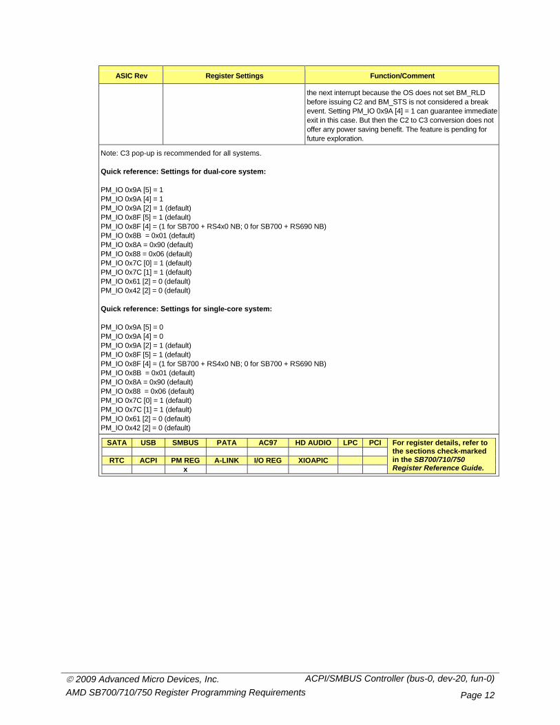
© 2009 Advanced Micro Devices, Inc. ACPI/SMBUS Controller (bus-0, dev-20, fun-0) AMD SB700/710/750 Register Programming Requirements Page 12
ASIC Rev Register Settings Function/Comment
the next interrupt because the OS does not set BM_RLD before issuing C2 and BM_STS is not considered a break event. Setting PM_IO 0x9A [4] = 1 can guarantee immediate exit in this case. But then the C2 to C3 conversion does not offer any power saving benefit. The feature is pending for future exploration.
Note: C3 pop-up is recommended for all systems. Quick reference: Settings for dual-core system: PM_IO 0x9A [5] = 1 PM_IO 0x9A [4] = 1 PM_IO 0x9A [2] = 1 (default) PM_IO 0x8F [5] = 1 (default) PM_IO 0x8F [4] = (1 for SB700 + RS4x0 NB; 0 for SB700 + RS690 NB) PM_IO 0x8B = 0x01 (default) PM_IO 0x8A = 0x90 (default) PM_IO 0x88 = 0x06 (default) PM_IO 0x7C [0] = 1 (default) PM_IO 0x7C [1] = 1 (default) PM_IO 0x61 [2] = 0 (default) PM_IO 0x42 [2] = 0 (default) Quick reference: Settings for single-core system: PM_IO 0x9A [5] = 0 PM_IO 0x9A [4] = 0 PM_IO 0x9A [2] = 1 (default) PM_IO 0x8F [5] = 1 (default) PM_IO 0x8F [4] = (1 for SB700 + RS4x0 NB; 0 for SB700 + RS690 NB) PM_IO 0x8B = 0x01 (default) PM_IO 0x8A = 0x90 (default) PM_IO 0x88 = 0x06 (default) PM_IO 0x7C [0] = 1 (default) PM_IO 0x7C [1] = 1 (default) PM_IO 0x61 [2] = 0 (default) PM_IO 0x42 [2] = 0 (default)
SATA USB SMBUS PATA AC97 HD AUDIO LPC PCI
RTC ACPI PM REG A-LINK I/O REG XIOAPIC x
For register details, refer to the sections check-marked in the SB700/710/750 Register Reference Guide.
© 2009 Advanced Micro Devices, Inc. ACPI/SMBUS Controller (bus-0, dev-20, fun-0) AMD SB700/710/750 Register Programming Requirements Page 13
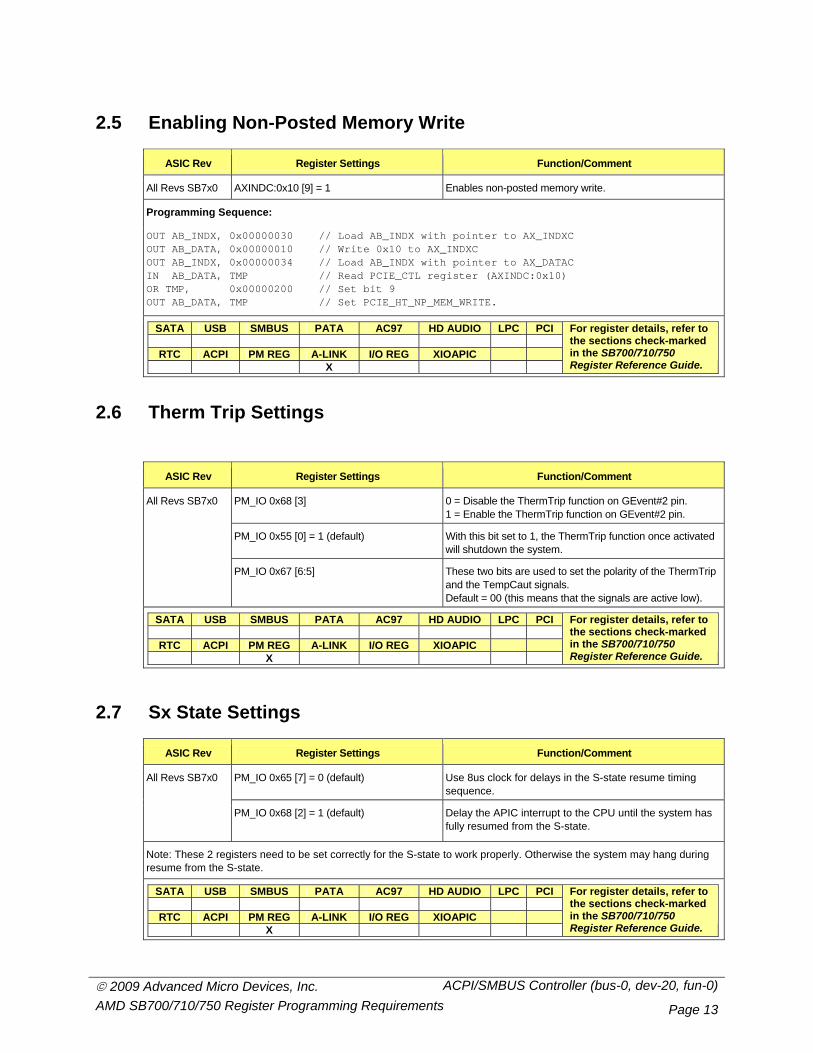
2.5 Enabling Non-Posted Memory Write
ASIC Rev Register Settings Function/Comment
All Revs SB7x0 AXINDC:0x10 [9] = 1 Enables non-posted memory write.
Programming Sequence:
OUT AB_INDX, 0x00000030 // Load AB_INDX with pointer to AX_INDXC OUT AB_DATA, 0x00000010 // Write 0x10 to AX_INDXC OUT AB_INDX, 0x00000034 // Load AB_INDX with pointer to AX_DATAC IN AB_DATA, TMP // Read PCIE_CTL register (AXINDC:0x10) OR TMP, 0x00000200 // Set bit 9 OUT AB_DATA, TMP // Set PCIE_HT_NP_MEM_WRITE.
SATA USB SMBUS PATA AC97 HD AUDIO LPC PCI
RTC ACPI PM REG A-LINK I/O REG XIOAPIC X
For register details, refer to the sections check-marked in the SB700/710/750 Register Reference Guide.
2.6 Therm Trip Settings
ASIC Rev Register Settings Function/Comment
PM_IO 0x68 [3] 0 = Disable the ThermTrip function on GEvent#2 pin. 1 = Enable the ThermTrip function on GEvent#2 pin.
PM_IO 0x55 [0] = 1 (default) With this bit set to 1, the ThermTrip function once activated will shutdown the system.
All Revs SB7x0
PM_IO 0x67 [6:5] These two bits are used to set the polarity of the ThermTrip and the TempCaut signals. Default = 00 (this means that the signals are active low).
SATA USB SMBUS PATA AC97 HD AUDIO LPC PCI
RTC ACPI PM REG A-LINK I/O REG XIOAPIC X
For register details, refer to the sections check-marked in the SB700/710/750 Register Reference Guide.
2.7 Sx State Settings
ASIC Rev Register Settings Function/Comment
PM_IO 0x65 [7] = 0 (default) Use 8us clock for delays in the S-state resume timing sequence.
All Revs SB7x0
PM_IO 0x68 [2] = 1 (default) Delay the APIC interrupt to the CPU until the system has fully resumed from the S-state.
Note: These 2 registers need to be set correctly for the S-state to work properly. Otherwise the system may hang during resume from the S-state.
SATA USB SMBUS PATA AC97 HD AUDIO LPC PCI
RTC ACPI PM REG A-LINK I/O REG XIOAPIC X
For register details, refer to the sections check-marked in the SB700/710/750 Register Reference Guide.
© 2009 Advanced Micro Devices, Inc. ACPI/SMBUS Controller (bus-0, dev-20, fun-0) AMD SB700/710/750 Register Programming Requirements Page 14
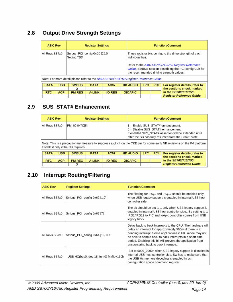
2.8 Output Drive Strength Settings
ASIC Rev Register Settings Function/Comment
All Revs SB7x0 Smbus_PCI_config 0xC0 [29:0] Setting TBD
These register bits configure the drive strength of each individual bus. Refer to the AMD SB700/710/750 Register Reference Guide, SMBUS section describing the PCI config C0h for the recommended driving strength values.
Note: For more detail please refer to the AMD SB700/710/750 Register Reference Guide.
SATA USB SMBUS PATA AC97 HD AUDIO LPC PCI X
RTC ACPI PM REG A-LINK I/O REG XIOAPIC
For register details, refer to the sections check-marked in the SB700/710/750 Register Reference Guide.
2.9 SUS_STAT# Enhancement
ASIC Rev Register Settings Function/Comment
All Revs SB7x0 PM_IO 0x7C[5] 1 = Enable SUS_STAT# enhancement. 0 = Disable SUS_STAT# enhancement. If enabled SUS_STAT# assertion will be extended until after the SB has fully resumed from the S3/4/5 state.
Note: This is a precautionary measure to suppress a glitch on the CKE pin for some early NB revisions on the P4 platform. Enable it only if the NB requires.
SATA USB SMBUS PATA AC97 HD AUDIO LPC PCI
RTC ACPI PM REG A-LINK I/O REG XIOAPIC X
For register details, refer to the sections check-marked in the SB700/710/750 Register Reference Guide.
2.10 Interrupt Routing/Filtering
ASIC Rev Register Settings Function/Comment
All Revs SB7x0 Smbus_PCI_config 0x62 [1:0] The filtering for IRQ1 and IRQ12 should be enabled only when USB legacy support is enabled in internal USB host controller side.
All Revs SB7x0 Smbus_PCI_config 0x67 [7]
The bit should be set to 1 only when USB legacy support is enabled in internal USB host controller side.. By setting to 1 IRQ1/IRQ12 to PIC and IoApic controller comes from USB legacy block.
All Revs SB7x0 Smbus_PCI_config 0x64 [13] = 1
Delay back to back interrupts to the CPU. The hardware will delay an interrupt for approximately 500ns if there is a pending interrupt. Some applications in PIC mode may not be able to handle back to back interrupts in a short time period. Enabling this bit will prevent the application from encountering back to back interrupts.
All Revs SB7x0 USB HC(bus0, dev 18, fun 0) MMio+160h
Set to 0000_0000h when USB legacy support is disabled in internal USB host controller side. Sw has to make sure that the USB Hc memory decoding is enabled in pci configuration space command register.
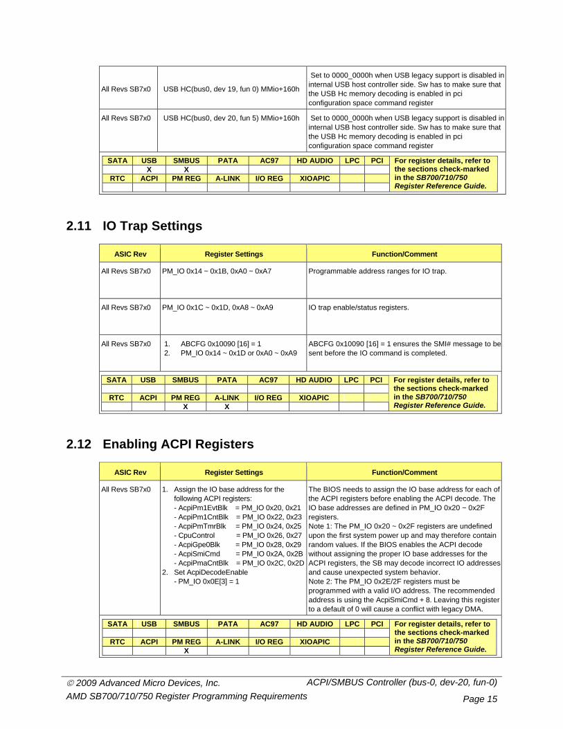
© 2009 Advanced Micro Devices, Inc. ACPI/SMBUS Controller (bus-0, dev-20, fun-0) AMD SB700/710/750 Register Programming Requirements Page 15
All Revs SB7x0 USB HC(bus0, dev 19, fun 0) MMio+160h
Set to 0000_0000h when USB legacy support is disabled in internal USB host controller side. Sw has to make sure that the USB Hc memory decoding is enabled in pci configuration space command register
All Revs SB7x0 USB HC(bus0, dev 20, fun 5) MMio+160h Set to 0000_0000h when USB legacy support is disabled in internal USB host controller side. Sw has to make sure that the USB Hc memory decoding is enabled in pci configuration space command register
SATA USB SMBUS PATA AC97 HD AUDIO LPC PCI X X
RTC ACPI PM REG A-LINK I/O REG XIOAPIC
For register details, refer to the sections check-marked in the SB700/710/750 Register Reference Guide.
2.11 IO Trap Settings
ASIC Rev Register Settings Function/Comment
All Revs SB7x0 PM_IO 0x14 ~ 0x1B, 0xA0 ~ 0xA7 Programmable address ranges for IO trap.
All Revs SB7x0 PM_IO 0x1C ~ 0x1D, 0xA8 ~ 0xA9 IO trap enable/status registers.
All Revs SB7x0 1. ABCFG 0x10090 [16] = 1 2. PM_IO 0x14 ~ 0x1D or 0xA0 ~ 0xA9
ABCFG 0x10090 [16] = 1 ensures the SMI# message to be sent before the IO command is completed.
SATA USB SMBUS PATA AC97 HD AUDIO LPC PCI
RTC ACPI PM REG A-LINK I/O REG XIOAPIC X X
For register details, refer to the sections check-marked in the SB700/710/750 Register Reference Guide.
2.12 Enabling ACPI Registers
ASIC Rev Register Settings Function/Comment
All Revs SB7x0 1. Assign the IO base address for the following ACPI registers: - AcpiPm1EvtBlk = PM_IO 0x20, 0x21 - AcpiPm1CntBlk = PM_IO 0x22, 0x23 - AcpiPmTmrBlk = PM_IO 0x24, 0x25 - CpuControl = PM_IO 0x26, 0x27 - AcpiGpe0Blk = PM_IO 0x28, 0x29 - AcpiSmiCmd = PM_IO 0x2A, 0x2B- AcpiPmaCntBlk = PM_IO 0x2C, 0x2D
2. Set AcpiDecodeEnable - PM_IO 0x0E[3] = 1
The BIOS needs to assign the IO base address for each of the ACPI registers before enabling the ACPI decode. The IO base addresses are defined in PM_IO 0x20 ~ 0x2F registers. Note 1: The PM_IO 0x20 ~ 0x2F registers are undefined upon the first system power up and may therefore contain random values. If the BIOS enables the ACPI decode without assigning the proper IO base addresses for the ACPI registers, the SB may decode incorrect IO addresses and cause unexpected system behavior. Note 2: The PM_IO 0x2E/2F registers must be programmed with a valid I/O address. The recommended address is using the AcpiSmiCmd + 8. Leaving this register to a default of 0 will cause a conflict with legacy DMA.
SATA USB SMBUS PATA AC97 HD AUDIO LPC PCI
RTC ACPI PM REG A-LINK I/O REG XIOAPIC X
For register details, refer to the sections check-marked in the SB700/710/750 Register Reference Guide.
© 2009 Advanced Micro Devices, Inc. ACPI/SMBUS Controller (bus-0, dev-20, fun-0) AMD SB700/710/750 Register Programming Requirements Page 16
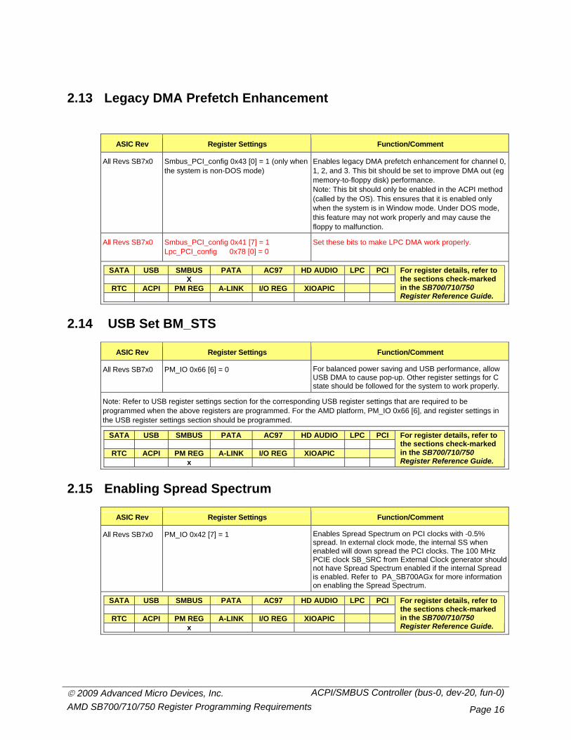
2.13 Legacy DMA Prefetch Enhancement
ASIC Rev Register Settings Function/Comment
All Revs SB7x0 Smbus_PCI_config 0x43 [0] = 1 (only when the system is non-DOS mode)
Enables legacy DMA prefetch enhancement for channel 0, 1, 2, and 3. This bit should be set to improve DMA out (eg memory-to-floppy disk) performance. Note: This bit should only be enabled in the ACPI method (called by the OS). This ensures that it is enabled only when the system is in Window mode. Under DOS mode, this feature may not work properly and may cause the floppy to malfunction.
All Revs SB7x0 Smbus_PCI_config 0x41 [7] = 1 Lpc_PCI_config 0x78 [0] = 0
Set these bits to make LPC DMA work properly.
SATA USB SMBUS PATA AC97 HD AUDIO LPC PCI X
RTC ACPI PM REG A-LINK I/O REG XIOAPIC
For register details, refer to the sections check-marked in the SB700/710/750 Register Reference Guide.
2.14 USB Set BM_STS
ASIC Rev Register Settings Function/Comment
All Revs SB7x0 PM_IO 0x66 [6] = 0 For balanced power saving and USB performance, allow USB DMA to cause pop-up. Other register settings for C state should be followed for the system to work properly.
Note: Refer to USB register settings section for the corresponding USB register settings that are required to be programmed when the above registers are programmed. For the AMD platform, PM_IO 0x66 [6], and register settings in the USB register settings section should be programmed.
SATA USB SMBUS PATA AC97 HD AUDIO LPC PCI
RTC ACPI PM REG A-LINK I/O REG XIOAPIC x
For register details, refer to the sections check-marked in the SB700/710/750 Register Reference Guide.
2.15 Enabling Spread Spectrum
ASIC Rev Register Settings Function/Comment
All Revs SB7x0 PM_IO 0x42 [7] = 1
Enables Spread Spectrum on PCI clocks with -0.5% spread. In external clock mode, the internal SS when enabled will down spread the PCI clocks. The 100 MHz PCIE clock SB_SRC from External Clock generator should not have Spread Spectrum enabled if the internal Spread is enabled. Refer to PA_SB700AGx for more information on enabling the Spread Spectrum.
SATA USB SMBUS PATA AC97 HD AUDIO LPC PCI
RTC ACPI PM REG A-LINK I/O REG XIOAPIC x
For register details, refer to the sections check-marked in the SB700/710/750 Register Reference Guide.
© 2009 Advanced Micro Devices, Inc. ACPI/SMBUS Controller (bus-0, dev-20, fun-0) AMD SB700/710/750 Register Programming Requirements Page 17
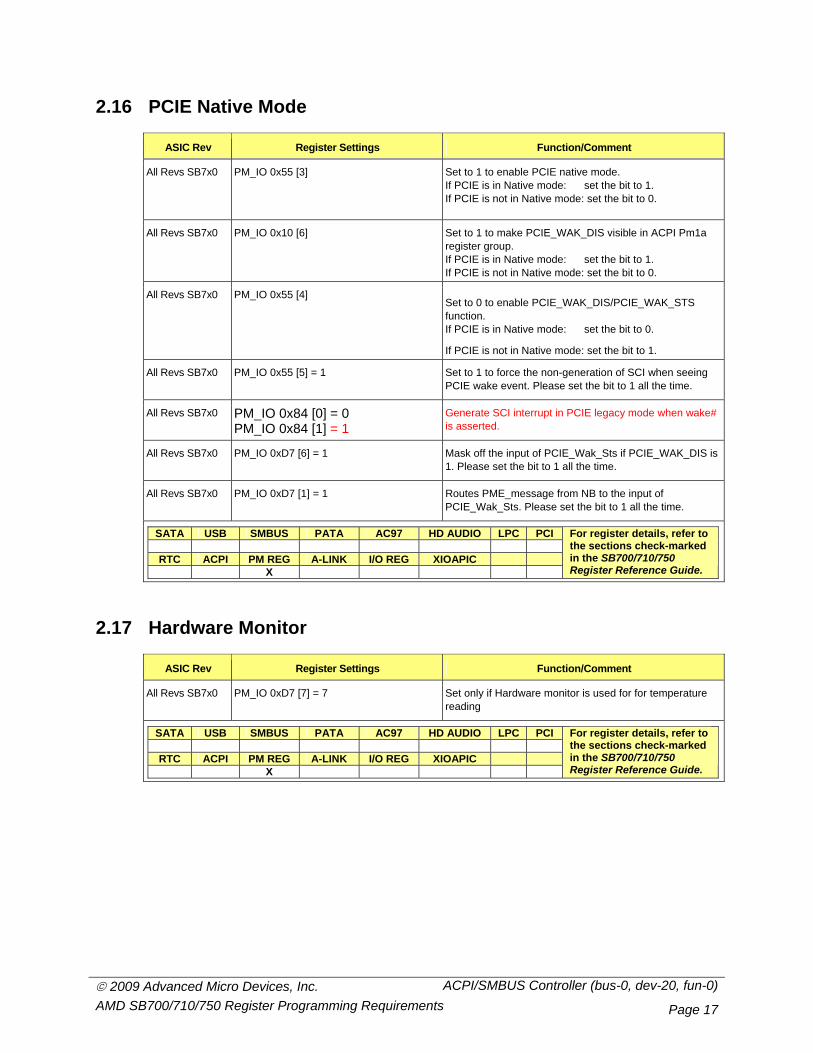
2.16 PCIE Native Mode
ASIC Rev Register Settings Function/Comment
All Revs SB7x0 PM_IO 0x55 [3]
Set to 1 to enable PCIE native mode. If PCIE is in Native mode: set the bit to 1. If PCIE is not in Native mode: set the bit to 0.
All Revs SB7x0 PM_IO 0x10 [6]
Set to 1 to make PCIE_WAK_DIS visible in ACPI Pm1a register group. If PCIE is in Native mode: set the bit to 1. If PCIE is not in Native mode: set the bit to 0.
All Revs SB7x0 PM_IO 0x55 [4] Set to 0 to enable PCIE_WAK_DIS/PCIE_WAK_STS
function. If PCIE is in Native mode: set the bit to 0.
If PCIE is not in Native mode: set the bit to 1.
All Revs SB7x0 PM_IO 0x55 [5] = 1 Set to 1 to force the non-generation of SCI when seeing PCIE wake event. Please set the bit to 1 all the time.
All Revs SB7x0 PM_IO 0x84 [0] = 0 PM_IO 0x84 [1] = 1
Generate SCI interrupt in PCIE legacy mode when wake# is asserted.
All Revs SB7x0 PM_IO 0xD7 [6] = 1 Mask off the input of PCIE_Wak_Sts if PCIE_WAK_DIS is 1. Please set the bit to 1 all the time.
All Revs SB7x0 PM_IO 0xD7 [1] = 1 Routes PME_message from NB to the input of PCIE_Wak_Sts. Please set the bit to 1 all the time.
SATA USB SMBUS PATA AC97 HD AUDIO LPC PCI
RTC ACPI PM REG A-LINK I/O REG XIOAPIC X
For register details, refer to the sections check-marked in the SB700/710/750 Register Reference Guide.
2.17 Hardware Monitor
ASIC Rev Register Settings Function/Comment
All Revs SB7x0 PM_IO 0xD7 [7] = 7 Set only if Hardware monitor is used for for temperature reading
SATA USB SMBUS PATA AC97 HD AUDIO LPC PCI
RTC ACPI PM REG A-LINK I/O REG XIOAPIC X
For register details, refer to the sections check-marked in the SB700/710/750 Register Reference Guide.
© 2009 Advanced Micro Devices, Inc. ACPI/SMBUS Controller (bus-0, dev-20, fun-0) AMD SB700/710/750 Register Programming Requirements Page 18
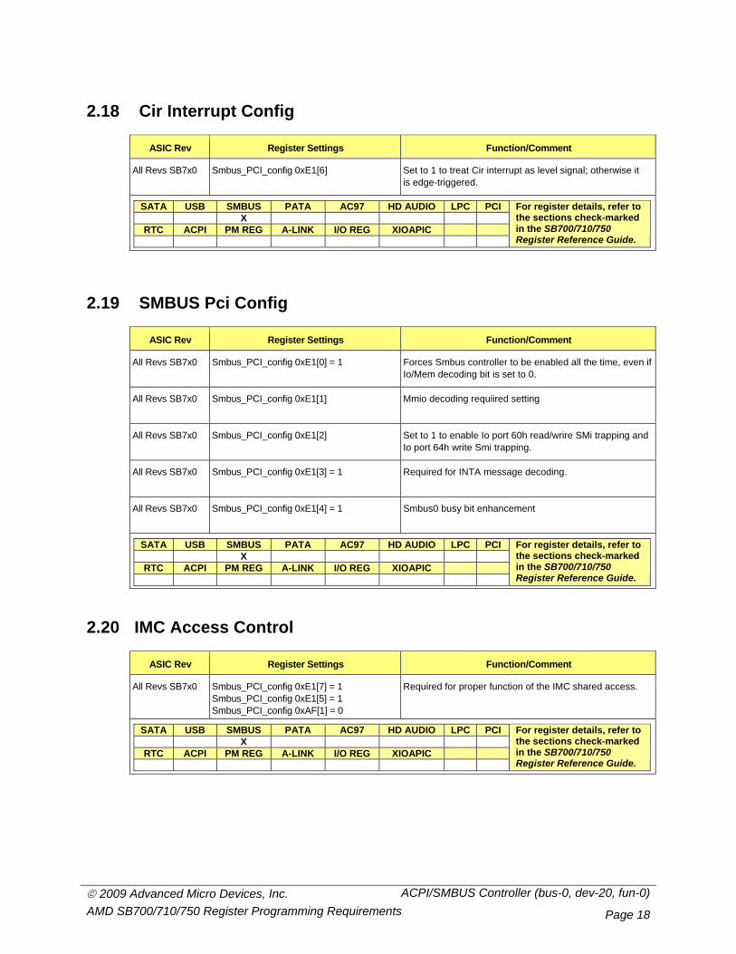
2.18 Cir Interrupt Config
ASIC Rev Register Settings Function/Comment
All Revs SB7x0 Smbus_PCI_config 0xE1[6] Set to 1 to treat Cir interrupt as level signal; otherwise it is edge-triggered.
SATA USB SMBUS PATA AC97 HD AUDIO LPC PCI X
RTC ACPI PM REG A-LINK I/O REG XIOAPIC
For register details, refer to the sections check-marked in the SB700/710/750 Register Reference Guide.
2.19 SMBUS Pci Config
ASIC Rev Register Settings Function/Comment
All Revs SB7x0 Smbus_PCI_config 0xE1[0] = 1 Forces Smbus controller to be enabled all the time, even if Io/Mem decoding bit is set to 0.
All Revs SB7x0 Smbus_PCI_config 0xE1[1] Mmio decoding requiired setting
All Revs SB7x0 Smbus_PCI_config 0xE1[2] Set to 1 to enable Io port 60h read/wrire SMi trapping and Io port 64h write Smi trapping.
All Revs SB7x0 Smbus_PCI_config 0xE1[3] = 1 Required for INTA message decoding.
All Revs SB7x0 Smbus_PCI_config 0xE1[4] = 1 Smbus0 busy bit enhancement
SATA USB SMBUS PATA AC97 HD AUDIO LPC PCI X
RTC ACPI PM REG A-LINK I/O REG XIOAPIC
For register details, refer to the sections check-marked in the SB700/710/750 Register Reference Guide.
2.20 IMC Access Control
ASIC Rev Register Settings Function/Comment
All Revs SB7x0 Smbus_PCI_config 0xE1[7] = 1 Smbus_PCI_config 0xE1[5] = 1 Smbus_PCI_config 0xAF[1] = 0
Required for proper function of the IMC shared access.
SATA USB SMBUS PATA AC97 HD AUDIO LPC PCI X
RTC ACPI PM REG A-LINK I/O REG XIOAPIC
For register details, refer to the sections check-marked in the SB700/710/750 Register Reference Guide.
© 2009 Advanced Micro Devices, Inc. ACPI/SMBUS Controller (bus-0, dev-20, fun-0) AMD SB700/710/750 Register Programming Requirements Page 19
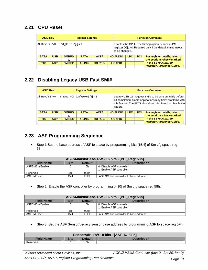
2.21 CPU Reset
ASIC Rev Register Settings Function/Comment
All Revs SB7x0 PM_IO 0xB2[2] = 1 Enables the CPU Reset timing option defined in PM register D5[1:0]. Required only if the default timing needs to be changed.
SATA USB SMBUS PATA AC97 HD AUDIO LPC PCI X
RTC ACPI PM REG A-LINK I/O REG XIOAPIC
For register details, refer to the sections check-marked in the SB700/710/750 Register Reference Guide.
2.22 Disabling Legacy USB Fast SMI#
ASIC Rev Register Settings Function/Comment
All Revs SB7x0 Smbus_PCI_config 0x62 [5] = 1 Legacy USB can request SMI# to be sent out early before IO completion. Some applications may have problems with this feature. The BIOS should set this bit to 1 to disable the feature.
SATA USB SMBUS PATA AC97 HD AUDIO LPC PCI x
RTC ACPI PM REG A-LINK I/O REG XIOAPIC
For register details, refer to the sections check-marked in the SB700/710/750 Register Reference Guide.
2.23 ASF Programming Sequence
• Step 1:Set the base address of ASF Io space by programming bits [15:4] of Sm cfg space reg 58h:
ASFSMbusIoBase- RW - 16 bits - [PCI_Reg: 58h] Field Name Bits Default Description
ASFSMBusEnable 0 0h 0: Disable ASF controller 1: Enable ASF controller
Reserved 3:1 000b ASFSMBase 15:4 FFFh ASF SM bus controller Io base address
• Step 2: Enable the ASF controller by programming bit [0] of Sm cfg space reg 58h:
ASFSMbusIoBase- RW - 16 bits - [PCI_Reg: 58h] Field Name Bits Default Description
ASFSMBusEnable 0 0h 0: Disable ASF controller 1: Enable ASF controller
Reserved 3:1 000b ASFSMBase 15:4 FFFh ASF SM bus controller Io base address
• Step 3: Set the ASF Sensor/Legacy sensor base address by programming ASF Io space reg 0Fh:
SensorAdr– RW - 8 bits - [ASF_IO: 0Fh] Field Name Bits Default Description
Reserved 0 0b
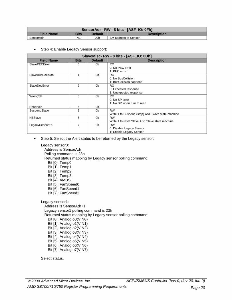
© 2009 Advanced Micro Devices, Inc. ACPI/SMBUS Controller (bus-0, dev-20, fun-0) AMD SB700/710/750 Register Programming Requirements Page 20
SensorAdr– RW - 8 bits - [ASF_IO: 0Fh] Field Name Bits Default Description
SensorAdr 7:1 00h SM address of Sensor.
• Step 4: Enable Legacy Sensor support:
SlaveMisc- RW - 8 bits - [ASF_IO: 0Dh] Field Name Bits Default Description
SlavePECError 0 0b RO 0: No PEC error 1: PEC error
SlaveBusCollision 1 0b RO 0: No BusCollision 1: BusCollision happens
SlaveDevError 2 0b RO 0: Expected response 1: Unexpected response
WrongSP 3 0b RO 0: No SP error 1: No SP when turn to read
Reserved 4 0b SuspendSlave 5 0b RW
Write 1 to Suspend (stop) ASF Slave state machine KillSlave 6 0b RW
Write 1 to reset Slave ASF Slave state machine LegacySensorEn 7 0b RW
0: Disable Legacy Sensor 1: Enable Legacy Sensor
• Step 5: Select the Alert status to be returned by the Legacy sensor:
Legacy sensor0: Address is SensorAdr Polling command is 23h Returned status mapping by Legacy sensor polling command:
Bit [0]: Temp0 Bit [1]: Temp1 Bit [2]: Temp2 Bit [3]: Temp3 Bit [4]: AMDSI Bit [5]: FanSpeed0 Bit [6]: FanSpeed1 Bit [7]: FanSpeed2
Legacy sensor1:
Address is SensorAdr+1 Legacy sensor1 polling command is 23h Returned status mapping by Legacy sensor polling command:
Bit [0]: AnalogIo0(VIN0) Bit [1]: AnalogIo1(VIN1) Bit [2]: AnalogIo2(VIN2) Bit [3]: AnalogIo3(VIN3) Bit [4]: AnalogIo4(VIN4) Bit [5]: AnalogIo5(VIN5) Bit [6]: AnalogIo6(VIN6) Bit [7]: AnalogIo7(VIN7)
Select status.
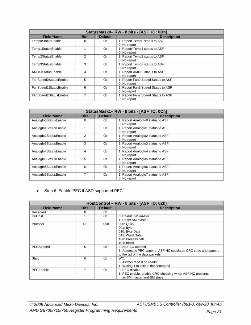
© 2009 Advanced Micro Devices, Inc. ACPI/SMBUS Controller (bus-0, dev-20, fun-0) AMD SB700/710/750 Register Programming Requirements Page 21
StatusMask0– RW - 8 bits - [ASF_IO: 0Bh] Field Name Bits Default Description
Temp0StatusEnable 0 0b 1: Report Temp0 status to ASF 0: No report
Temp1StatusEnable 1 0b 1: Report Temp1 status to ASF 0: No report
Temp2StatusEnable 2 0b 1: Report Temp2 status to ASF 0: No report
Temp3StatusEnable 3 0b 1: Report Temp3 status to ASF 0: No report
AMDSIStatusEnable 4 0b 1: Report AMDSI status to ASF 0: No report
FanSpeed0StatusEnable 5 0b 1: Report Fan0 Speed Status to ASF 0: No report
FanSpeed1StatusEnable 6 0b 1: Report Fan1 Speed Status to ASF 0: No report
FanSpeed2StatusEnable 7 0b 1: Report Fan2 Speed Status to ASF 0: No report
StatusMask1– RW - 8 bits - [ASF_IO: 0Ch] Field Name Bits Default Description
AnalogIo0StatusEnable 0 0b 1: Report AnalogIo0 status to ASF 0: No report
AnalogIo1StatusEnable 1 0b 1: Report AnalogIo1 status to ASF 0: No report
AnalogIo2StatusEnable 2 0b 1: Report AnalogIo2 status to ASF 0: No report
AnalogIo3StatusEnable 3 0b 1: Report AnalogIo3 status to ASF 0: No report
AnalogIo4StatusEnable 4 0b 1: Report AnalogIo4 status to ASF 0: No report
AnalogIo5StatusEnable 5 0b 1: Report AnalogIo5 status to ASF 0: No report
AnalogIo6StatusEnable 6 0b 1: Report AnalogIo6 status to ASF 0: No report
AnalogIo7StatusEnable 7 0b 1: Report AnalogIo7 status to ASF 0: No report
• Step 6: Enable PEC if ASD supported PEC:
HostControl – RW - 8 bits - [ASF_IO: 02h] Field Name Bits Default Description
Reserved 0 0b KillHost 1 0b 0: Enable SM master
1: Reset SM master Protocol 4:2 000b 000: Quick
001: Byte 010: Byte Data 011: Word Data 100: Process call 101: Block
PECAppend 5 0b 0: No PEC append 1: Automatic PEC append. ASF HC caculates CRC code and append to the tail of the data packets.
Start 6 0b WO: 0: Always read 0 on reads 1: Writing 1 to initiate the command
PECEnable 7 0b 0: PEC disable 1: PEC enable, enable CRC checking when ASF HC presents as SM master and SM slave.
© 2009 Advanced Micro Devices, Inc. ACPI/SMBUS Controller (bus-0, dev-20, fun-0) AMD SB700/710/750 Register Programming Requirements Page 22
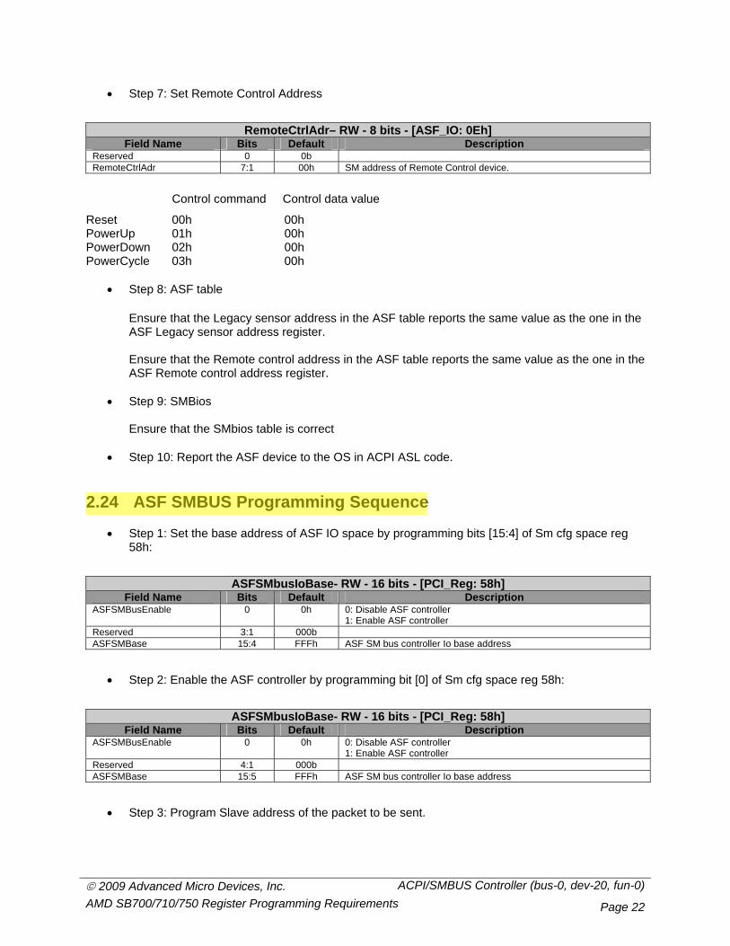
• Step 7: Set Remote Control Address
RemoteCtrlAdr– RW - 8 bits - [ASF_IO: 0Eh] Field Name Bits Default Description
Reserved 0 0b RemoteCtrlAdr 7:1 00h SM address of Remote Control device.
Control command Control data value
Reset 00h 00h PowerUp 01h 00h PowerDown 02h 00h PowerCycle 03h 00h
• Step 8: ASF table
Ensure that the Legacy sensor address in the ASF table reports the same value as the one in the ASF Legacy sensor address register. Ensure that the Remote control address in the ASF table reports the same value as the one in the ASF Remote control address register.
• Step 9: SMBios
Ensure that the SMbios table is correct
• Step 10: Report the ASF device to the OS in ACPI ASL code.
2.24 ASF SMBUS Programming Sequence
• Step 1: Set the base address of ASF IO space by programming bits [15:4] of Sm cfg space reg 58h:
ASFSMbusIoBase- RW - 16 bits - [PCI_Reg: 58h] Field Name Bits Default Description
ASFSMBusEnable 0 0h 0: Disable ASF controller 1: Enable ASF controller
Reserved 3:1 000b ASFSMBase 15:4 FFFh ASF SM bus controller Io base address
• Step 2: Enable the ASF controller by programming bit [0] of Sm cfg space reg 58h:
ASFSMbusIoBase- RW - 16 bits - [PCI_Reg: 58h] Field Name Bits Default Description
ASFSMBusEnable 0 0h 0: Disable ASF controller 1: Enable ASF controller
Reserved 4:1 000b ASFSMBase 15:5 FFFh ASF SM bus controller Io base address
• Step 3: Program Slave address of the packet to be sent.
© 2009 Advanced Micro Devices, Inc. ACPI/SMBUS Controller (bus-0, dev-20, fun-0) AMD SB700/710/750 Register Programming Requirements Page 23
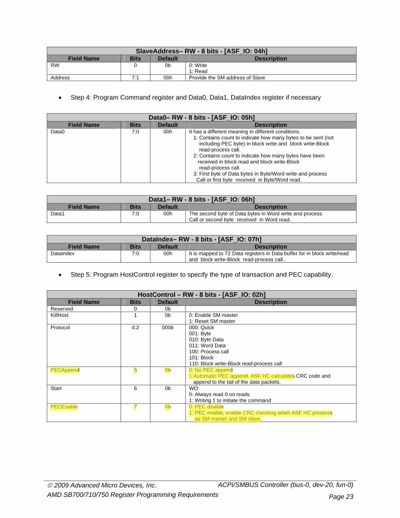
SlaveAddress– RW - 8 bits - [ASF_IO: 04h] Field Name Bits Default Description
RW 0 0b 0: Write 1: Read
Address 7:1 00h Provide the SM address of Slave
• Step 4: Program Command register and Data0, Data1, DataIndex register if necessary
Data0– RW - 8 bits - [ASF_IO: 05h] Field Name Bits Default Description
Data0 7:0 00h It has a different meaning in different conditions. 1: Contains count to indicate how many bytes to be sent (not including PEC byte) in block write and block write-Block read-process call. 2: Contains count to indicate how many bytes have been received in block read and block write-Block read-process call. 3: First byte of Data bytes in Byte/Word write and process Call or first byte received in Byte/Word read.
Data1– RW - 8 bits - [ASF_IO: 06h] Field Name Bits Default Description
Data1 7:0 00h The second byte of Data bytes in Word write and process Call or second byte received in Word read.
DataIndex– RW - 8 bits - [ASF_IO: 07h] Field Name Bits Default Description
DataIndex 7:0 00h It is mapped to 72 Data registers in Data buffer for in block write/read and block write-Block read-process call..
• Step 5: Program HostControl register to specify the type of transaction and PEC capability.
HostControl – RW - 8 bits - [ASF_IO: 02h] Field Name Bits Default Description
Reserved 0 0b KillHost 1 0b 0: Enable SM master
1: Reset SM master Protocol 4:2 000b 000: Quick
001: Byte 010: Byte Data 011: Word Data 100: Process call 101: Block 110: Block write-Block read-process call
PECAppend 5 0b 0: No PEC append 1:Automatic PEC append. ASF HC calculates CRC code and append to the tail of the data packets.
Start 6 0b WO: 0: Always read 0 on reads 1: Writing 1 to initiate the command
PECEnable 7 0b 0: PEC disable 1: PEC enable, enable CRC checking when ASF HC presents as SM master and SM slave.
© 2009 Advanced Micro Devices, Inc. ACPI/SMBUS Controller (bus-0, dev-20, fun-0) AMD SB700/710/750 Register Programming Requirements Page 24
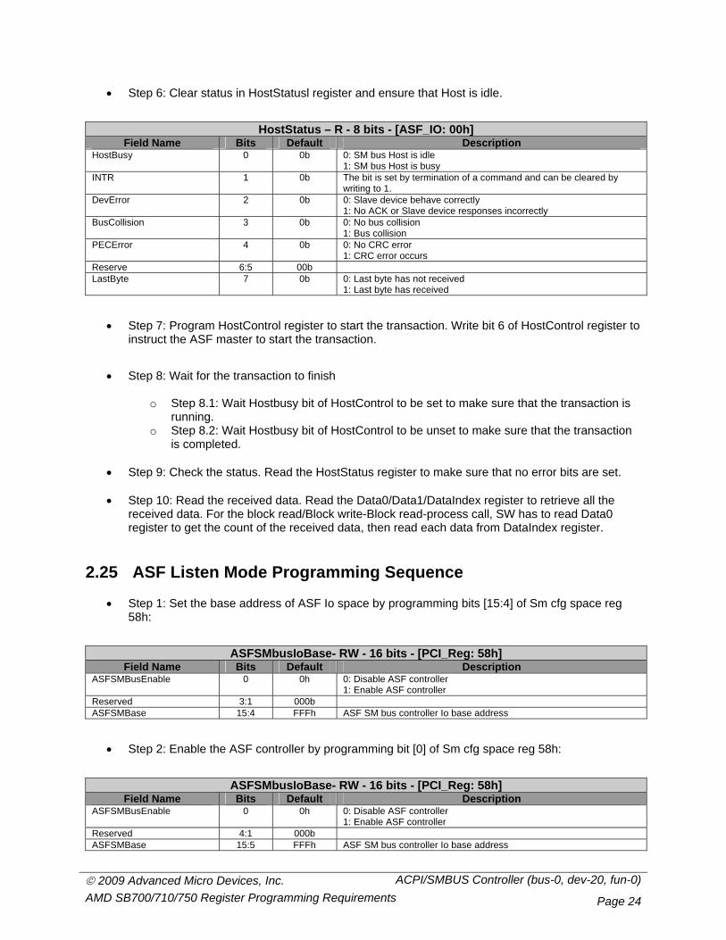
• Step 6: Clear status in HostStatusl register and ensure that Host is idle.
HostStatus – R - 8 bits - [ASF_IO: 00h] Field Name Bits Default Description
HostBusy 0 0b 0: SM bus Host is idle 1: SM bus Host is busy
INTR 1 0b The bit is set by termination of a command and can be cleared by writing to 1.
DevError 2 0b 0: Slave device behave correctly 1: No ACK or Slave device responses incorrectly
BusCollision 3 0b 0: No bus collision 1: Bus collision
PECError 4 0b 0: No CRC error 1: CRC error occurs
Reserve 6:5 00b LastByte 7 0b 0: Last byte has not received
1: Last byte has received
• Step 7: Program HostControl register to start the transaction. Write bit 6 of HostControl register to instruct the ASF master to start the transaction.
• Step 8: Wait for the transaction to finish
o Step 8.1: Wait Hostbusy bit of HostControl to be set to make sure that the transaction is running.
o Step 8.2: Wait Hostbusy bit of HostControl to be unset to make sure that the transaction is completed.
• Step 9: Check the status. Read the HostStatus register to make sure that no error bits are set. • Step 10: Read the received data. Read the Data0/Data1/DataIndex register to retrieve all the
received data. For the block read/Block write-Block read-process call, SW has to read Data0 register to get the count of the received data, then read each data from DataIndex register.
2.25 ASF Listen Mode Programming Sequence
• Step 1: Set the base address of ASF Io space by programming bits [15:4] of Sm cfg space reg 58h:
ASFSMbusIoBase- RW - 16 bits - [PCI_Reg: 58h] Field Name Bits Default Description
ASFSMBusEnable 0 0h 0: Disable ASF controller 1: Enable ASF controller
Reserved 3:1 000b ASFSMBase 15:4 FFFh ASF SM bus controller Io base address
• Step 2: Enable the ASF controller by programming bit [0] of Sm cfg space reg 58h:
ASFSMbusIoBase- RW - 16 bits - [PCI_Reg: 58h] Field Name Bits Default Description
ASFSMBusEnable 0 0h 0: Disable ASF controller 1: Enable ASF controller
Reserved 4:1 000b ASFSMBase 15:5 FFFh ASF SM bus controller Io base address
© 2009 Advanced Micro Devices, Inc. ACPI/SMBUS Controller (bus-0, dev-20, fun-0) AMD SB700/710/750 Register Programming Requirements Page 25
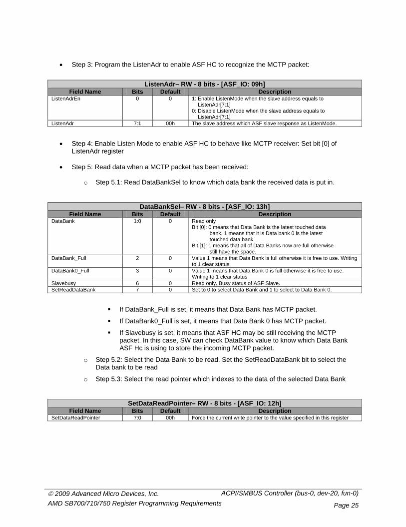
• Step 3: Program the ListenAdr to enable ASF HC to recognize the MCTP packet:
ListenAdr– RW - 8 bits - [ASF_IO: 09h] Field Name Bits Default Description
ListenAdrEn 0 0 1: Enable ListenMode when the slave address equals to ListenAdr[7:1] 0: Disable ListenMode when the slave address equals to ListenAdr[7:1]
ListenAdr 7:1 00h The slave address which ASF slave response as ListenMode.
• Step 4: Enable Listen Mode to enable ASF HC to behave like MCTP receiver: Set bit [0] of ListenAdr register
• Step 5: Read data when a MCTP packet has been received:
o Step 5.1: Read DataBankSel to know which data bank the received data is put in.
DataBankSel– RW - 8 bits - [ASF_IO: 13h] Field Name Bits Default Description
DataBank 1:0 0 Read only Bit [0]: 0 means that Data Bank is the latest touched data bank, 1 means that it is Data bank 0 is the latest touched data bank. Bit [1]: 1 means that all of Data Banks now are full otherwise still have the space.
DataBank_Full 2 0 Value 1 means that Data Bank is full otherwise it is free to use. Writing to 1 clear status
DataBank0_Full 3 0 Value 1 means that Data Bank 0 is full otherwise it is free to use. Writing to 1 clear status
Slavebusy 6 0 Read only. Busy status of ASF Slave. SetReadDataBank 7 0 Set to 0 to select Data Bank and 1 to select to Data Bank 0.
If DataBank_Full is set, it means that Data Bank has MCTP packet.
If DataBank0_Full is set, it means that Data Bank 0 has MCTP packet.
If Slavebusy is set, it means that ASF HC may be still receiving the MCTP packet. In this case, SW can check DataBank value to know which Data Bank ASF Hc is using to store the incoming MCTP packet.
o Step 5.2: Select the Data Bank to be read. Set the SetReadDataBank bit to select the Data bank to be read
o Step 5.3: Select the read pointer which indexes to the data of the selected Data Bank
SetDataReadPointer– RW - 8 bits - [ASF_IO: 12h] Field Name Bits Default Description
SetDataReadPointer 7:0 00h Force the current write pointer to the value specified in this register
© 2009 Advanced Micro Devices, Inc. ACPI/SMBUS Controller (bus-0, dev-20, fun-0) AMD SB700/710/750 Register Programming Requirements Page 26
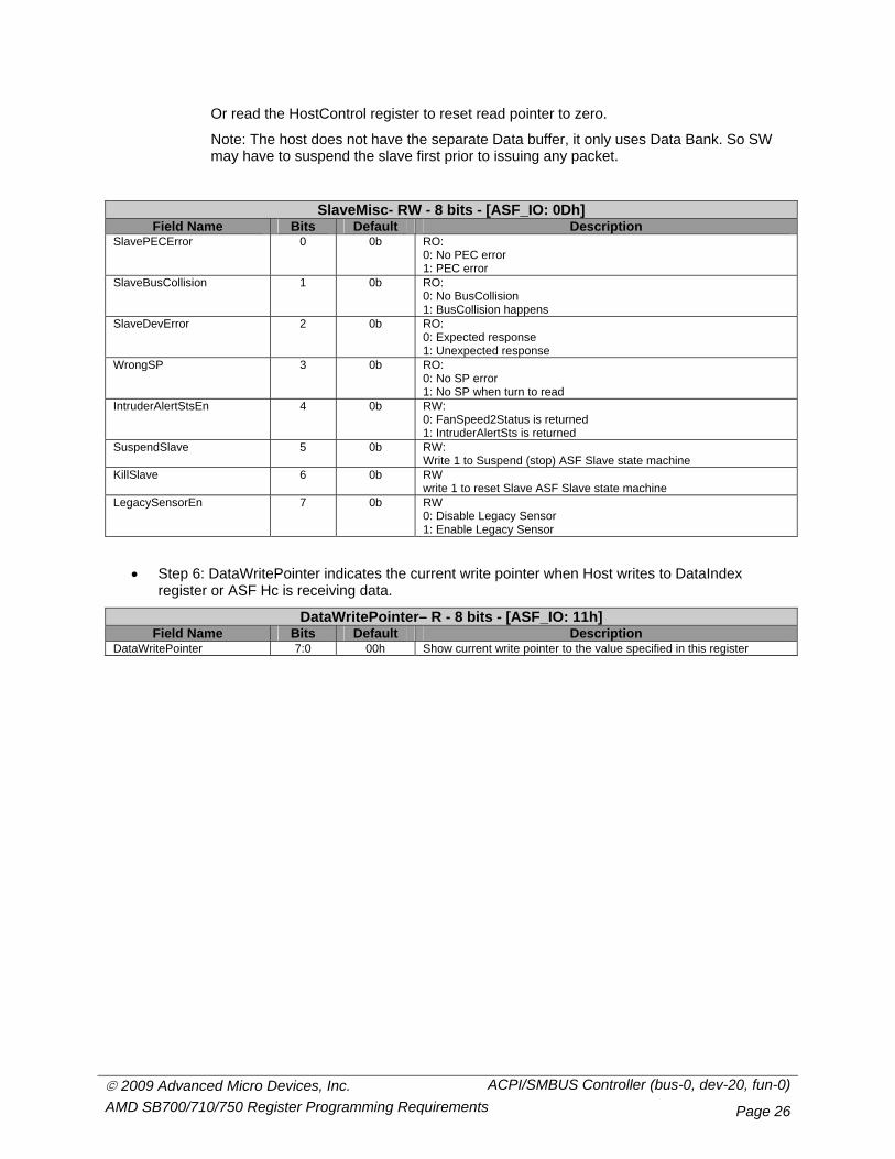
Or read the HostControl register to reset read pointer to zero.
Note: The host does not have the separate Data buffer, it only uses Data Bank. So SW may have to suspend the slave first prior to issuing any packet.
SlaveMisc- RW - 8 bits - [ASF_IO: 0Dh] Field Name Bits Default Description
SlavePECError 0 0b RO: 0: No PEC error 1: PEC error
SlaveBusCollision 1 0b RO: 0: No BusCollision 1: BusCollision happens
SlaveDevError 2 0b RO: 0: Expected response 1: Unexpected response
WrongSP 3 0b RO: 0: No SP error 1: No SP when turn to read
IntruderAlertStsEn 4 0b RW: 0: FanSpeed2Status is returned 1: IntruderAlertSts is returned
SuspendSlave 5 0b RW: Write 1 to Suspend (stop) ASF Slave state machine
KillSlave 6 0b RW write 1 to reset Slave ASF Slave state machine
LegacySensorEn 7 0b RW 0: Disable Legacy Sensor 1: Enable Legacy Sensor
• Step 6: DataWritePointer indicates the current write pointer when Host writes to DataIndex register or ASF Hc is receiving data.
DataWritePointer– R - 8 bits - [ASF_IO: 11h] Field Name Bits Default Description
DataWritePointer 7:0 00h Show current write pointer to the value specified in this register
© 2009 Advanced Micro Devices, Inc. ACPI/SMBUS Controller (bus-0, dev-20, fun-0) AMD SB700/710/750 Register Programming Requirements Page 27
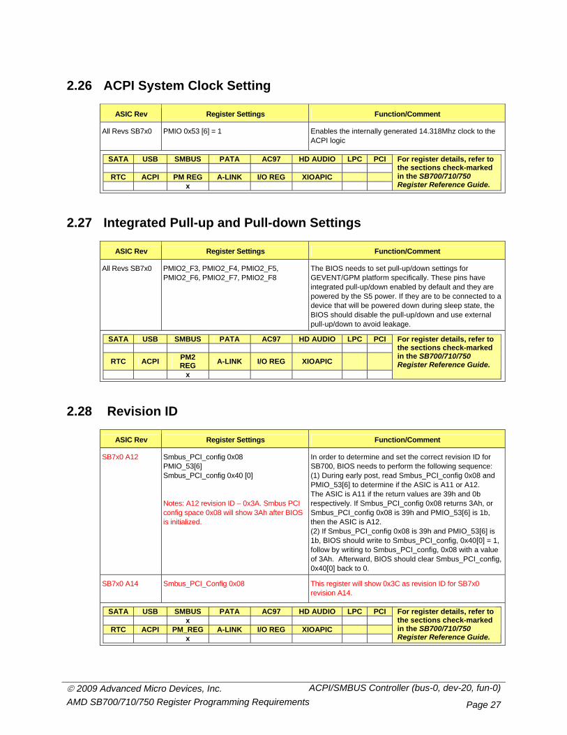
2.26 ACPI System Clock Setting
ASIC Rev Register Settings Function/Comment
All Revs SB7x0 PMIO 0x53 [6] = 1 Enables the internally generated 14.318Mhz clock to the ACPI logic
SATA USB SMBUS PATA AC97 HD AUDIO LPC PCI
RTC ACPI PM REG A-LINK I/O REG XIOAPIC x
For register details, refer to the sections check-marked in the SB700/710/750 Register Reference Guide.
2.27 Integrated Pull-up and Pull-down Settings
ASIC Rev Register Settings Function/Comment
All Revs SB7x0 PMIO2_F3, PMIO2_F4, PMIO2_F5, PMIO2_F6, PMIO2_F7, PMIO2_F8
The BIOS needs to set pull-up/down settings for GEVENT/GPM platform specifically. These pins have integrated pull-up/down enabled by default and they are powered by the S5 power. If they are to be connected to a device that will be powered down during sleep state, the BIOS should disable the pull-up/down and use external pull-up/down to avoid leakage.
SATA USB SMBUS PATA AC97 HD AUDIO LPC PCI
RTC ACPI PM2 REG A-LINK I/O REG XIOAPIC
x
For register details, refer to the sections check-marked in the SB700/710/750 Register Reference Guide.
2.28 Revision ID
ASIC Rev Register Settings Function/Comment
SB7x0 A12 Smbus_PCI_config 0x08 PMIO_53[6] Smbus_PCI_config 0x40 [0] Notes: A12 revision ID – 0x3A. Smbus PCI config space 0x08 will show 3Ah after BIOS is initialized.
In order to determine and set the correct revision ID for SB700, BIOS needs to perform the following sequence: (1) During early post, read Smbus_PCI_config 0x08 and PMIO_53[6] to determine if the ASIC is A11 or A12. The ASIC is A11 if the return values are 39h and 0b respectively. If Smbus_PCI_config 0x08 returns 3Ah, or Smbus_PCI_config 0x08 is 39h and PMIO_53[6] is 1b, then the ASIC is A12. (2) If Smbus_PCI_config 0x08 is 39h and PMIO_53[6] is 1b, BIOS should write to Smbus_PCI_config, 0x40[0] = 1, follow by writing to Smbus_PCI_config, 0x08 with a value of 3Ah. Afterward, BIOS should clear Smbus_PCI_config, 0x40[0] back to 0.
SB7x0 A14 Smbus_PCI_Config 0x08 This register will show 0x3C as revision ID for SB7x0 revision A14.
SATA USB SMBUS PATA AC97 HD AUDIO LPC PCI x
RTC ACPI PM_REG A-LINK I/O REG XIOAPIC x
For register details, refer to the sections check-marked in the SB700/710/750 Register Reference Guide.
© 2009 Advanced Micro Devices, Inc. ACPI/SMBUS Controller (bus-0, dev-20, fun-0) AMD SB700/710/750 Register Programming Requirements Page 28
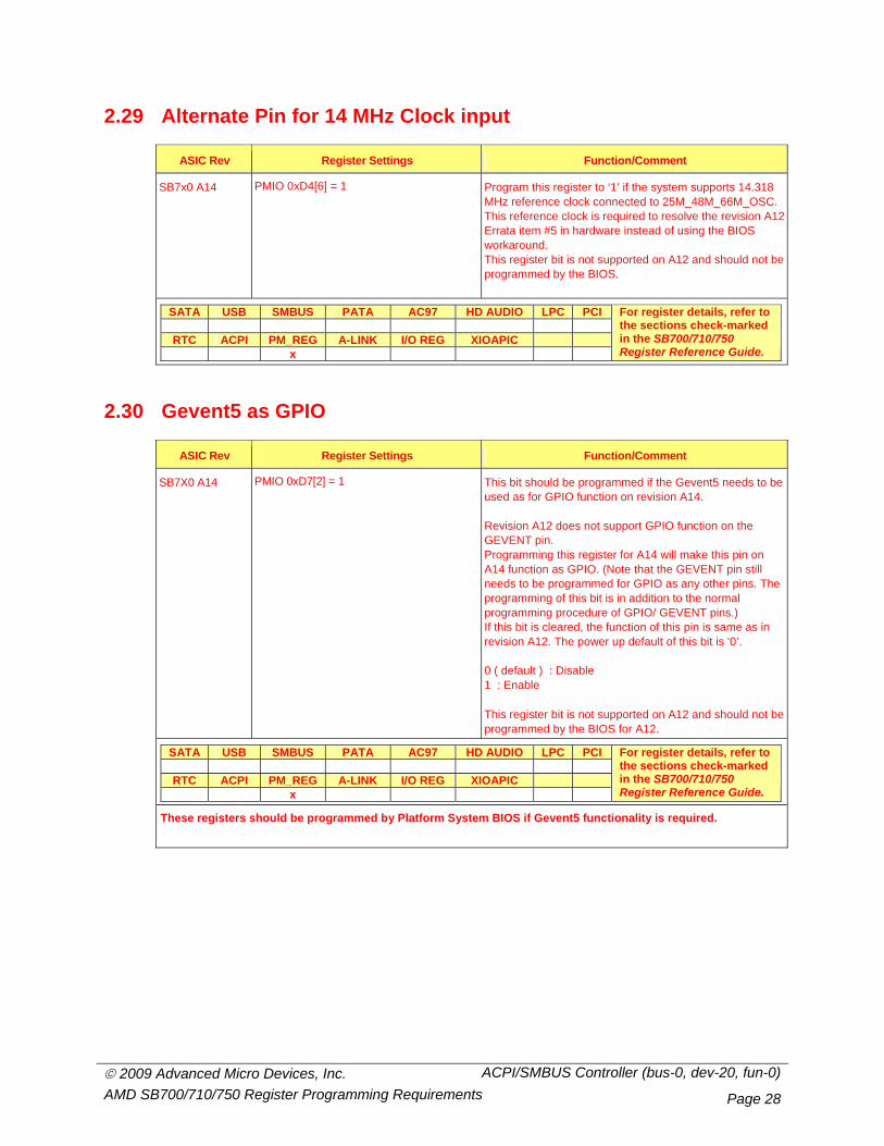
2.29 Alternate Pin for 14 MHz Clock input
ASIC Rev Register Settings Function/Comment
SB7x0 A14
PMIO 0xD4[6] = 1
Program this register to ‘1’ if the system supports 14.318 MHz reference clock connected to 25M_48M_66M_OSC. This reference clock is required to resolve the revision A12 Errata item #5 in hardware instead of using the BIOS workaround. This register bit is not supported on A12 and should not be programmed by the BIOS.
SATA USB SMBUS PATA AC97 HD AUDIO LPC PCI
RTC ACPI PM_REG A-LINK I/O REG XIOAPIC x
For register details, refer to the sections check-marked in the SB700/710/750 Register Reference Guide.
2.30 Gevent5 as GPIO
ASIC Rev Register Settings Function/Comment
SB7X0 A14
PMIO 0xD7[2] = 1
This bit should be programmed if the Gevent5 needs to be used as for GPIO function on revision A14. Revision A12 does not support GPIO function on the GEVENT pin. Programming this register for A14 will make this pin on A14 function as GPIO. (Note that the GEVENT pin still needs to be programmed for GPIO as any other pins. The programming of this bit is in addition to the normal programming procedure of GPIO/ GEVENT pins.) If this bit is cleared, the function of this pin is same as in revision A12. The power up default of this bit is ‘0’. 0 ( default ) : Disable 1 : Enable This register bit is not supported on A12 and should not be programmed by the BIOS for A12.
SATA USB SMBUS PATA AC97 HD AUDIO LPC PCI
RTC ACPI PM_REG A-LINK I/O REG XIOAPIC x
For register details, refer to the sections check-marked in the SB700/710/750 Register Reference Guide.
These registers should be programmed by Platform System BIOS if Gevent5 functionality is required.
© 2009 Advanced Micro Devices, Inc. ACPI/SMBUS Controller (bus-0, dev-20, fun-0) AMD SB700/710/750 Register Programming Requirements Page 29
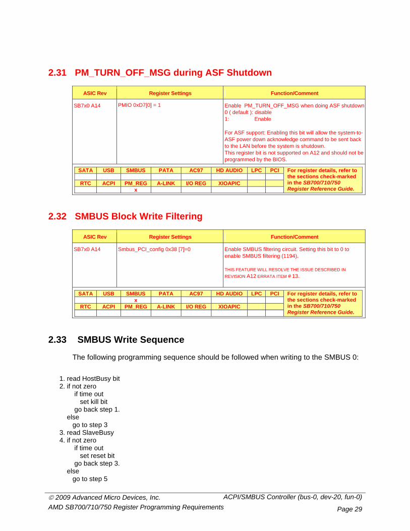
2.31 PM_TURN_OFF_MSG during ASF Shutdown
ASIC Rev Register Settings Function/Comment
SB7x0 A14
PMIO 0xD7[0] = 1
Enable PM_TURN_OFF_MSG when doing ASF shutdown 0 ( default ): disable 1: Enable For ASF support: Enabling this bit will allow the system-to-ASF power down acknowledge command to be sent back to the LAN before the system is shutdown. This register bit is not supported on A12 and should not be programmed by the BIOS.
SATA USB SMBUS PATA AC97 HD AUDIO LPC PCI
RTC ACPI PM_REG A-LINK I/O REG XIOAPIC x
For register details, refer to the sections check-marked in the SB700/710/750 Register Reference Guide.
2.32 SMBUS Block Write Filtering
ASIC Rev Register Settings Function/Comment
SB7x0 A14
Smbus_PCI_config 0x38 [7]=0
Enable SMBUS filtering circuit. Setting this bit to 0 to enable SMBUS filtering (1194). THIS FEATURE WILL RESOLVE THE ISSUE DESCRIBED IN REVISION A12 ERRATA ITEM # 13.
SATA USB SMBUS PATA AC97 HD AUDIO LPC PCI x
RTC ACPI PM_REG A-LINK I/O REG XIOAPIC
For register details, refer to the sections check-marked in the SB700/710/750 Register Reference Guide.
2.33 SMBUS Write Sequence
The following programming sequence should be followed when writing to the SMBUS 0:
1. read HostBusy bit 2. if not zero if time out set kill bit go back step 1. else go to step 3 3. read SlaveBusy 4. if not zero if time out set reset bit go back step 3. else go to step 5
© 2009 Advanced Micro Devices, Inc. ACPI/SMBUS Controller (bus-0, dev-20, fun-0) AMD SB700/710/750 Register Programming Requirements Page 30
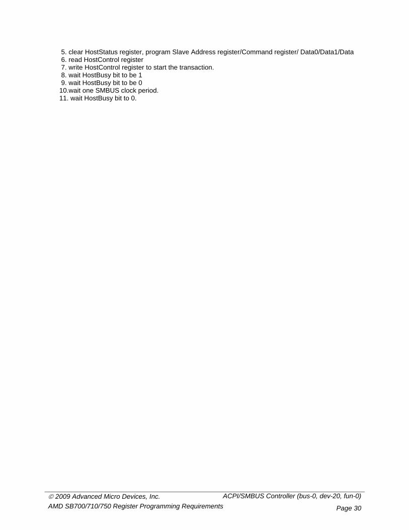
5. clear HostStatus register, program Slave Address register/Command register/ Data0/Data1/Data 6. read HostControl register 7. write HostControl register to start the transaction. 8. wait HostBusy bit to be 1 9. wait HostBusy bit to be 0 10.wait one SMBUS clock period. 11. wait HostBusy bit to 0.
© 2009 Advanced Micro Devices, Inc. LPC Controller (bus-0, dev-20, fun-3) AMD SB700/710/750 Register Programming Requirements Page 31
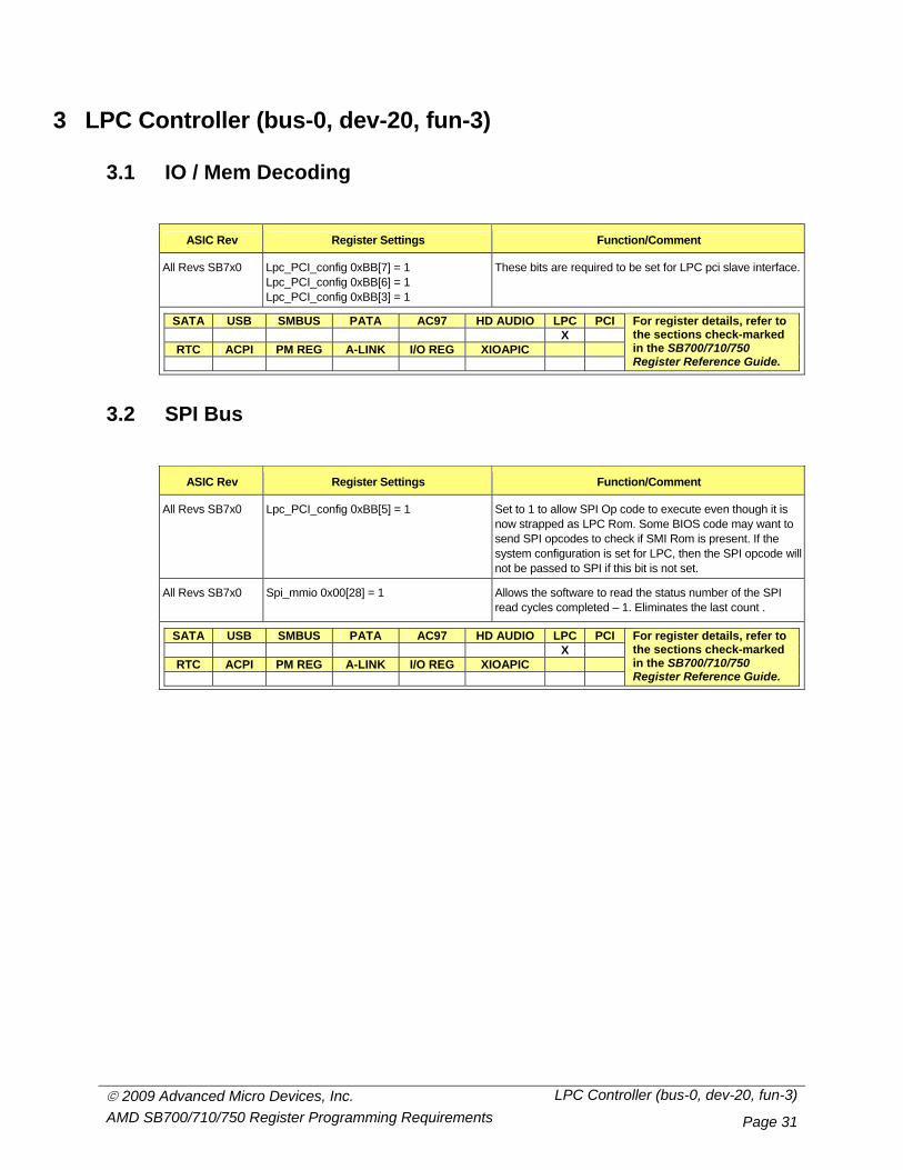
3 LPC Controller (bus-0, dev-20, fun-3)
3.1 IO / Mem Decoding
ASIC Rev Register Settings Function/Comment
All Revs SB7x0 Lpc_PCI_config 0xBB[7] = 1 Lpc_PCI_config 0xBB[6] = 1 Lpc_PCI_config 0xBB[3] = 1
These bits are required to be set for LPC pci slave interface.
SATA USB SMBUS PATA AC97 HD AUDIO LPC PCI X
RTC ACPI PM REG A-LINK I/O REG XIOAPIC
For register details, refer to the sections check-marked in the SB700/710/750 Register Reference Guide.
3.2 SPI Bus
ASIC Rev Register Settings Function/Comment
All Revs SB7x0 Lpc_PCI_config 0xBB[5] = 1
Set to 1 to allow SPI Op code to execute even though it is now strapped as LPC Rom. Some BIOS code may want to send SPI opcodes to check if SMI Rom is present. If the system configuration is set for LPC, then the SPI opcode will not be passed to SPI if this bit is not set.
All Revs SB7x0 Spi_mmio 0x00[28] = 1
Allows the software to read the status number of the SPI read cycles completed – 1. Eliminates the last count .
SATA USB SMBUS PATA AC97 HD AUDIO LPC PCI X
RTC ACPI PM REG A-LINK I/O REG XIOAPIC
For register details, refer to the sections check-marked in the SB700/710/750 Register Reference Guide.
© 2009 Advanced Micro Devices, Inc. A-Link Express Settings - Indirect I/O Access AMD SB700/710/750 Register Programming Requirements Page 32
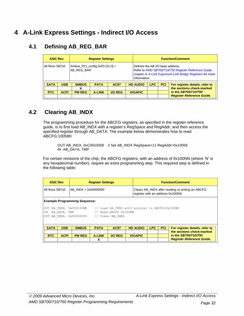
4 A-Link Express Settings - Indirect I/O Access
4.1 Defining AB_REG_BAR
ASIC Rev Register Settings Function/Comment
All Revs SB7x0 Smbus_PCI_config 0xF0 [31:0] = AB_REG_BAR
Defines the AB I/O base address. Refer to AMD SB700/710/750 Register Reference Guide, chapter 4: A-Link Express/A-Link Bridge Registers for more information.
SATA USB SMBUS PATA AC97 HD AUDIO LPC PCI X
RTC ACPI PM REG A-LINK I/O REG XIOAPIC
For register details, refer to the sections check-marked in the SB700/710/750 Register Reference Guide.
4.2 Clearing AB_INDX
The programming procedure for the ABCFG registers, as specified in the register reference guide, is to first load AB_INDX with a register’s RegSpace and RegAddr; and then access the specified register through AB_DATA. The example below demonstrates how to read ABCFG:10058h:
OUT AB_INDX, 0xC0010058 // Set AB_INDX RegSpace=11 RegAddr=0x10058 IN AB_DATA, TMP
For certain revisions of the chip, the ABCFG registers, with an address of 0x100NN (where ‘N’ is any hexadecimal number), require an extra programming step. This required step is defined in the following table:
ASIC Rev Register Settings Function/Comment
All Revs SB7x0 AB_INDX = 0x00000000 Clears AB_INDX after reading or writing an ABCFG register with an address 0x100NN.
Example Programming Sequence:
OUT AB_INDX, 0xC00100NN // Load AB_INDX with pointer to ABCFG:0x100NN IN AB_DATA, TMP // Read ABCFG 0x100NN OUT AB_INDX, 0x00000000 // Clear AB_INDX
SATA USB SMBUS PATA AC97 HD AUDIO LPC PCI
RTC ACPI PM REG A-LINK I/O REG XIOAPIC X
For register details, refer to the sections check-marked in the SB700/710/750 Register Reference Guide.
© 2009 Advanced Micro Devices, Inc. A-Link Express Settings - Indirect I/O Access AMD SB700/710/750 Register Programming Requirements Page 33
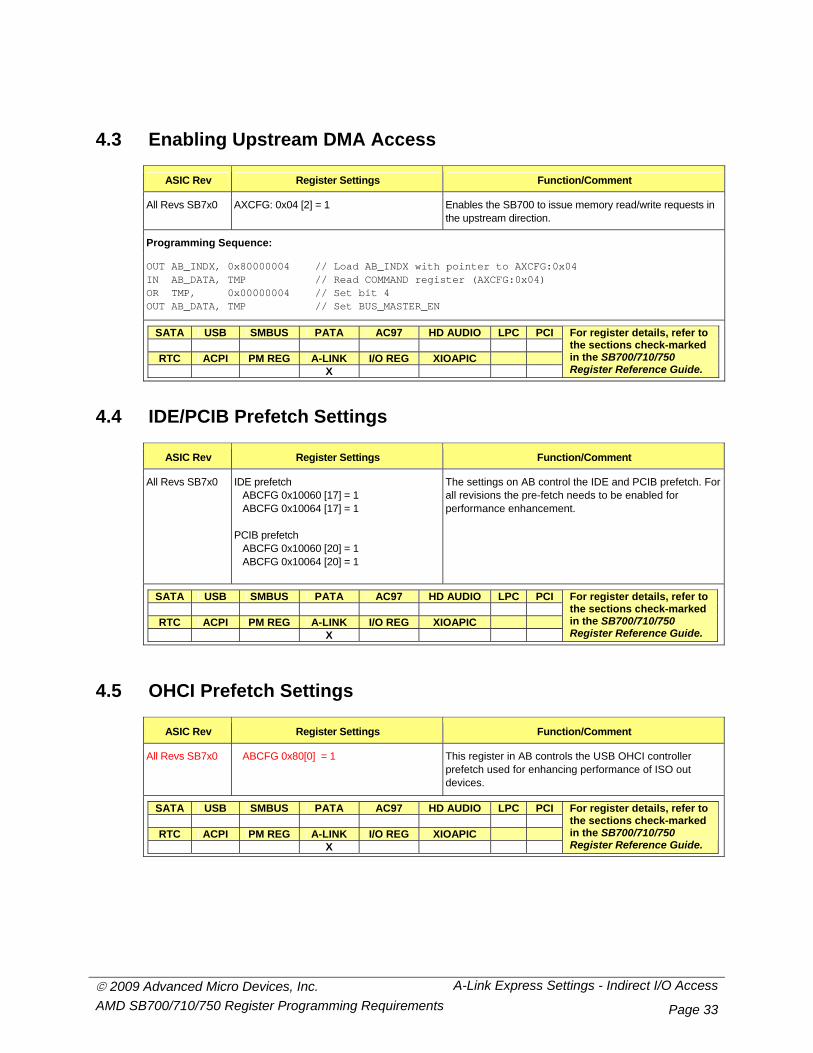
4.3 Enabling Upstream DMA Access
ASIC Rev Register Settings Function/Comment
All Revs SB7x0 AXCFG: 0x04 [2] = 1 Enables the SB700 to issue memory read/write requests in the upstream direction.
Programming Sequence:
OUT AB_INDX, 0x80000004 // Load AB_INDX with pointer to AXCFG:0x04 IN AB_DATA, TMP // Read COMMAND register (AXCFG:0x04) OR TMP, 0x00000004 // Set bit 4 OUT AB_DATA, TMP // Set BUS_MASTER_EN
SATA USB SMBUS PATA AC97 HD AUDIO LPC PCI
RTC ACPI PM REG A-LINK I/O REG XIOAPIC X
For register details, refer to the sections check-marked in the SB700/710/750 Register Reference Guide.
4.4 IDE/PCIB Prefetch Settings
ASIC Rev Register Settings Function/Comment
All Revs SB7x0 IDE prefetch ABCFG 0x10060 [17] = 1 ABCFG 0x10064 [17] = 1 PCIB prefetch ABCFG 0x10060 [20] = 1 ABCFG 0x10064 [20] = 1
The settings on AB control the IDE and PCIB prefetch. For all revisions the pre-fetch needs to be enabled for performance enhancement.
SATA USB SMBUS PATA AC97 HD AUDIO LPC PCI
RTC ACPI PM REG A-LINK I/O REG XIOAPIC X
For register details, refer to the sections check-marked in the SB700/710/750 Register Reference Guide.
4.5 OHCI Prefetch Settings
ASIC Rev Register Settings Function/Comment
All Revs SB7x0
ABCFG 0x80[0] = 1
This register in AB controls the USB OHCI controller prefetch used for enhancing performance of ISO out devices.
SATA USB SMBUS PATA AC97 HD AUDIO LPC PCI
RTC ACPI PM REG A-LINK I/O REG XIOAPIC X
For register details, refer to the sections check-marked in the SB700/710/750 Register Reference Guide.
© 2009 Advanced Micro Devices, Inc. A-Link Express Settings - Indirect I/O Access AMD SB700/710/750 Register Programming Requirements Page 34
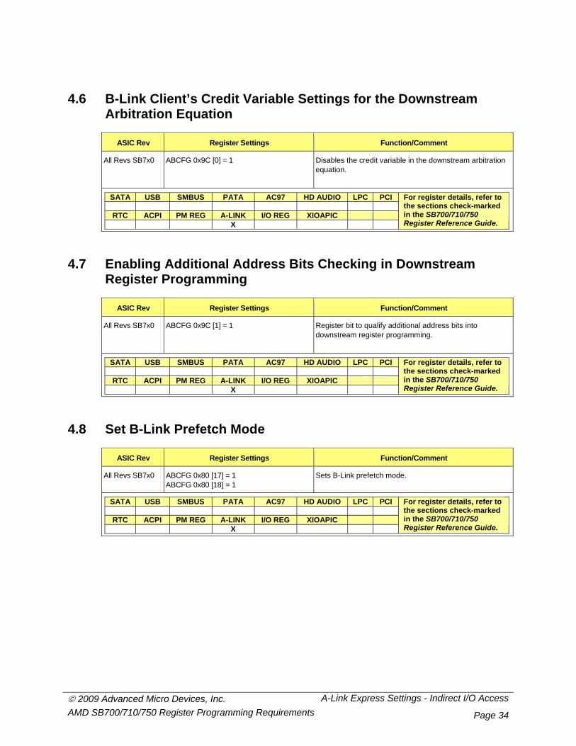
4.6 B-Link Client’s Credit Variable Settings for the Downstream Arbitration Equation
ASIC Rev Register Settings Function/Comment
All Revs SB7x0 ABCFG 0x9C [0] = 1 Disables the credit variable in the downstream arbitration equation.
SATA USB SMBUS PATA AC97 HD AUDIO LPC PCI
RTC ACPI PM REG A-LINK I/O REG XIOAPIC X
For register details, refer to the sections check-marked in the SB700/710/750 Register Reference Guide.
4.7 Enabling Additional Address Bits Checking in Downstream Register Programming
ASIC Rev Register Settings Function/Comment
All Revs SB7x0 ABCFG 0x9C [1] = 1
Register bit to qualify additional address bits into downstream register programming.
SATA USB SMBUS PATA AC97 HD AUDIO LPC PCI
RTC ACPI PM REG A-LINK I/O REG XIOAPIC X
For register details, refer to the sections check-marked in the SB700/710/750 Register Reference Guide.
4.8 Set B-Link Prefetch Mode
ASIC Rev Register Settings Function/Comment
All Revs SB7x0 ABCFG 0x80 [17] = 1 ABCFG 0x80 [18] = 1
Sets B-Link prefetch mode.
SATA USB SMBUS PATA AC97 HD AUDIO LPC PCI
RTC ACPI PM REG A-LINK I/O REG XIOAPIC X
For register details, refer to the sections check-marked in the SB700/710/750 Register Reference Guide.
© 2009 Advanced Micro Devices, Inc. A-Link Express Settings - Indirect I/O Access AMD SB700/710/750 Register Programming Requirements Page 35
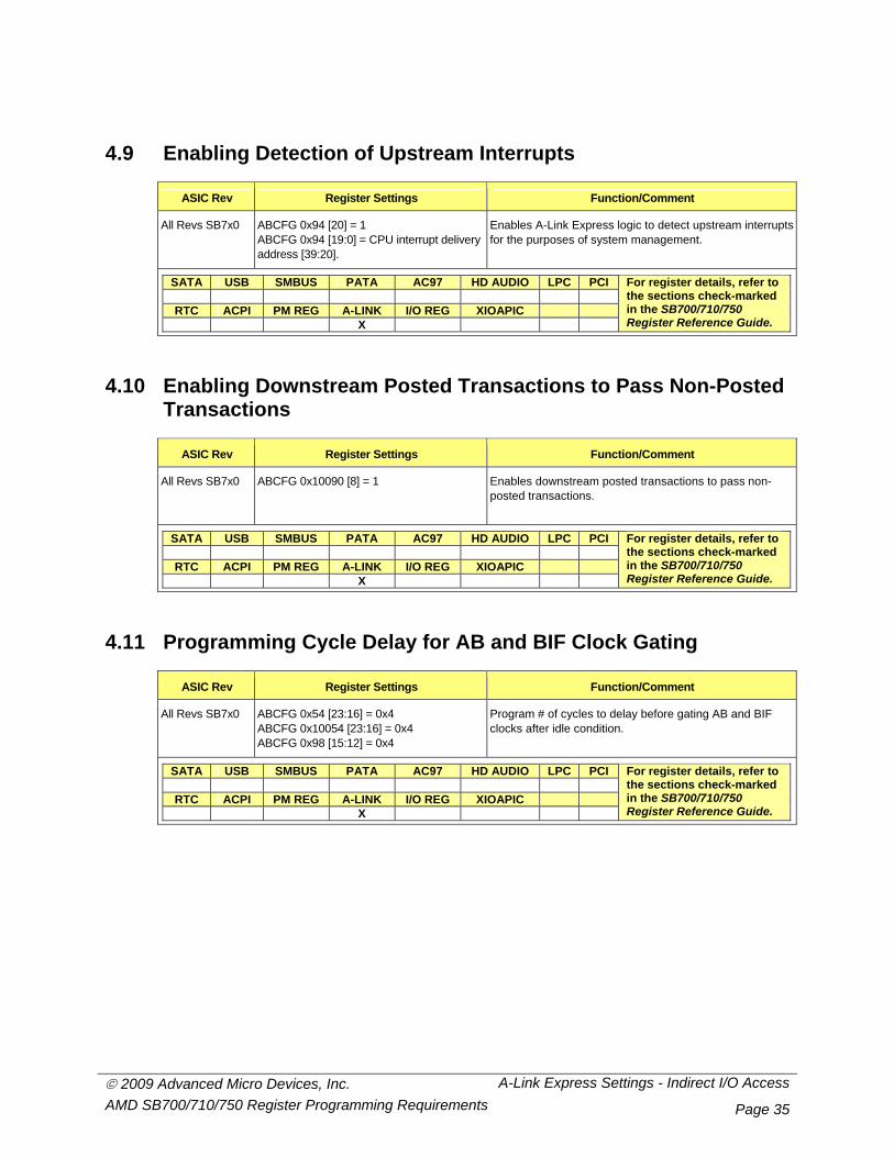
4.9 Enabling Detection of Upstream Interrupts
ASIC Rev Register Settings Function/Comment
All Revs SB7x0
ABCFG 0x94 [20] = 1 ABCFG 0x94 [19:0] = CPU interrupt delivery address [39:20].
Enables A-Link Express logic to detect upstream interrupts for the purposes of system management.
SATA USB SMBUS PATA AC97 HD AUDIO LPC PCI
RTC ACPI PM REG A-LINK I/O REG XIOAPIC X
For register details, refer to the sections check-marked in the SB700/710/750 Register Reference Guide.
4.10 Enabling Downstream Posted Transactions to Pass Non-Posted Transactions
ASIC Rev Register Settings Function/Comment
All Revs SB7x0
ABCFG 0x10090 [8] = 1 Enables downstream posted transactions to pass non-posted transactions.
SATA USB SMBUS PATA AC97 HD AUDIO LPC PCI
RTC ACPI PM REG A-LINK I/O REG XIOAPIC X
For register details, refer to the sections check-marked in the SB700/710/750 Register Reference Guide.
4.11 Programming Cycle Delay for AB and BIF Clock Gating
ASIC Rev Register Settings Function/Comment
All Revs SB7x0
ABCFG 0x54 [23:16] = 0x4 ABCFG 0x10054 [23:16] = 0x4 ABCFG 0x98 [15:12] = 0x4
Program # of cycles to delay before gating AB and BIF clocks after idle condition.
SATA USB SMBUS PATA AC97 HD AUDIO LPC PCI
RTC ACPI PM REG A-LINK I/O REG XIOAPIC X
For register details, refer to the sections check-marked in the SB700/710/750 Register Reference Guide.
© 2009 Advanced Micro Devices, Inc. A-Link Express Settings - Indirect I/O Access AMD SB700/710/750 Register Programming Requirements Page 36
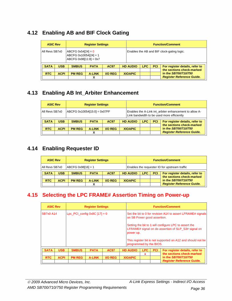
4.12 Enabling AB and BIF Clock Gating
ASIC Rev Register Settings Function/Comment
All Revs SB7x0
ABCFG 0x54[24] = 0 ABCFG 0x10054[24] = 1 ABCFG 0x98[11:8] = 0x7
Enables the AB and BIF clock-gating logic.
SATA USB SMBUS PATA AC97 HD AUDIO LPC PCI
RTC ACPI PM REG A-LINK I/O REG XIOAPIC X
For register details, refer to the sections check-marked in the SB700/710/750 Register Reference Guide.
4.13 Enabling AB Int_Arbiter Enhancement
ASIC Rev Register Settings Function/Comment
All Revs SB7x0
ABCFG 0x10054[15:0] = 0x07FF Enables the A-Link int_arbiter enhancement to allow A-Link bandwidth to be used more efficiently
SATA USB SMBUS PATA AC97 HD AUDIO LPC PCI
RTC ACPI PM REG A-LINK I/O REG XIOAPIC X
For register details, refer to the sections check-marked in the SB700/710/750 Register Reference Guide.
4.14 Enabling Requester ID
ASIC Rev Register Settings Function/Comment
All Revs SB7x0 ABCFG 0x98[16] = 1 Enables the requester ID for upstream traffic
SATA USB SMBUS PATA AC97 HD AUDIO LPC PCI
RTC ACPI PM REG A-LINK I/O REG XIOAPIC X
For register details, refer to the sections check-marked in the SB700/710/750 Register Reference Guide.
4.15 Selecting the LPC FRAME# Assertion Timing on Power-up
ASIC Rev Register Settings Function/Comment
SB7x0 A14
Lpc_PCI_config 0x8C [17] = 0
Set the bit to 0 for revision A14 to assert LFRAME# signals on SB Power good assertion. Setting the bit to 1 will configure LPC to assert the LFRAME# signal on de-assertion of SLP_S3# signal on power up. This register bit is not supported on A12 and should not be programmed by the BIOS.
SATA USB SMBUS PATA AC97 HD AUDIO LPC PCI x
RTC ACPI PM REG A-LINK I/O REG XIOAPIC
For register details, refer to the sections check-marked in the SB700/710/750 Register Reference Guide.
© 2009 Advanced Micro Devices, Inc. A-Link Express Settings - Indirect I/O Access AMD SB700/710/750 Register Programming Requirements Page 37
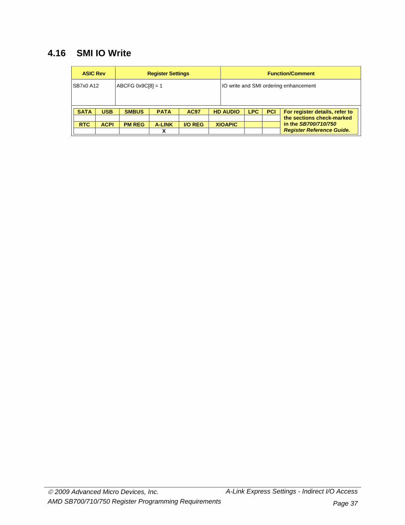
4.16 SMI IO Write
ASIC Rev Register Settings Function/Comment
SB7x0 A12
ABCFG 0x9C[8] = 1 IO write and SMI ordering enhancement
SATA USB SMBUS PATA AC97 HD AUDIO LPC PCI
RTC ACPI PM REG A-LINK I/O REG XIOAPIC X
For register details, refer to the sections check-marked in the SB700/710/750 Register Reference Guide.
© 2009 Advanced Micro Devices, Inc. PCIB (PCI-bridge, bus-0, dev-20, fun-04) AMD SB700/710/750 Register Programming Requirements Page 38
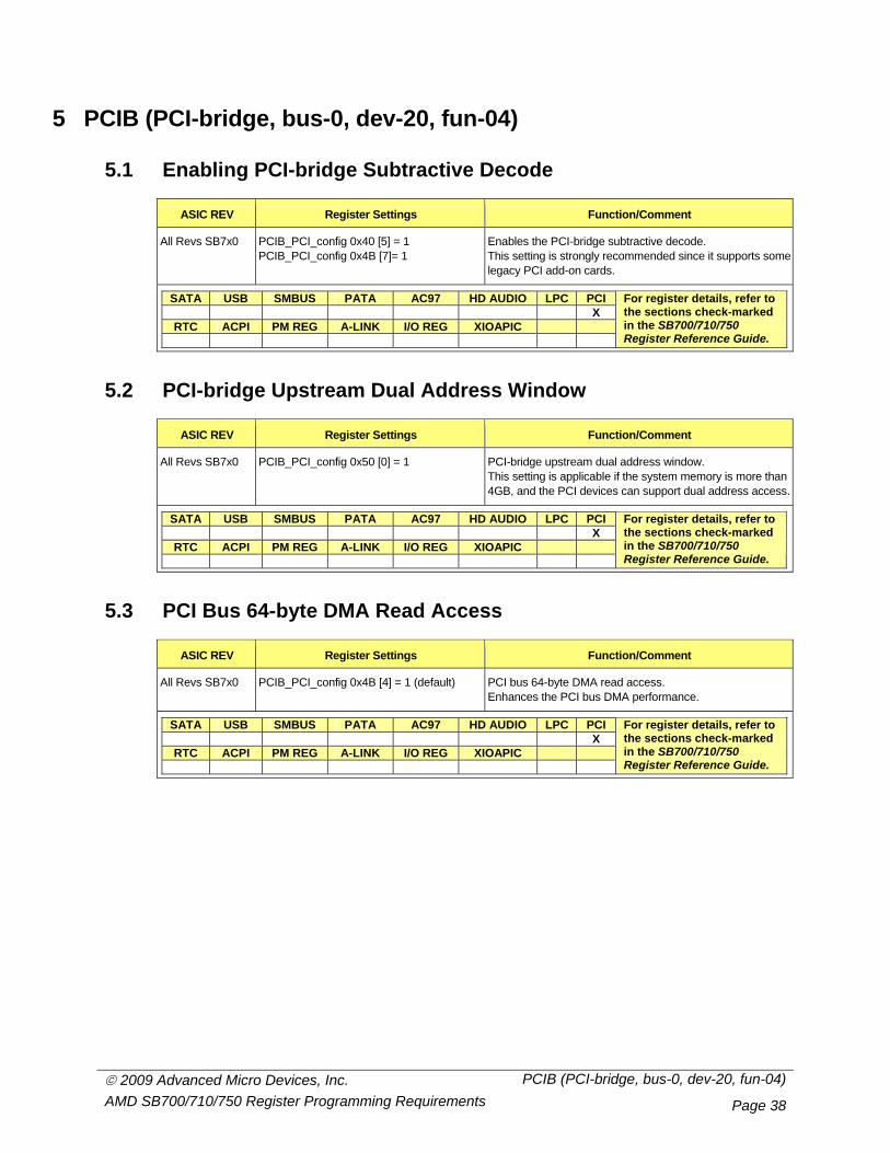
5 PCIB (PCI-bridge, bus-0, dev-20, fun-04)
5.1 Enabling PCI-bridge Subtractive Decode
ASIC REV Register Settings Function/Comment
All Revs SB7x0 PCIB_PCI_config 0x40 [5] = 1 PCIB_PCI_config 0x4B [7]= 1
Enables the PCI-bridge subtractive decode. This setting is strongly recommended since it supports some legacy PCI add-on cards.
SATA USB SMBUS PATA AC97 HD AUDIO LPC PCI X
RTC ACPI PM REG A-LINK I/O REG XIOAPIC
For register details, refer to the sections check-marked in the SB700/710/750 Register Reference Guide.
5.2 PCI-bridge Upstream Dual Address Window
ASIC REV Register Settings Function/Comment
All Revs SB7x0 PCIB_PCI_config 0x50 [0] = 1 PCI-bridge upstream dual address window. This setting is applicable if the system memory is more than 4GB, and the PCI devices can support dual address access.
SATA USB SMBUS PATA AC97 HD AUDIO LPC PCI X
RTC ACPI PM REG A-LINK I/O REG XIOAPIC
For register details, refer to the sections check-marked in the SB700/710/750 Register Reference Guide.
5.3 PCI Bus 64-byte DMA Read Access
ASIC REV Register Settings Function/Comment
All Revs SB7x0 PCIB_PCI_config 0x4B [4] = 1 (default) PCI bus 64-byte DMA read access. Enhances the PCI bus DMA performance.
SATA USB SMBUS PATA AC97 HD AUDIO LPC PCI X
RTC ACPI PM REG A-LINK I/O REG XIOAPIC
For register details, refer to the sections check-marked in the SB700/710/750 Register Reference Guide.
© 2009 Advanced Micro Devices, Inc. PCIB (PCI-bridge, bus-0, dev-20, fun-04) AMD SB700/710/750 Register Programming Requirements Page 39
5.4 PCI Bus DMA Write Cacheline Alignment
ASIC REV Register Settings Function/Comment
All Revs SB7x0 PCIB_PCI_config 0x40 [1] = 1 (default) Enables the PCIB writes to be cacheline aligned. The size of the writes will be set in the Cacheline Register (PCIB_PCI_config 0x4B[4:0]). Refer to section 5.3 for more information.
SATA USB SMBUS PATA AC97 HD AUDIO LPC PCI X
RTC ACPI PM REG A-LINK I/O REG XIOAPIC
For register details, refer to the sections check-marked in the SB700/710/750 Register Reference Guide.
5.5 Master Latency Timer
ASIC REV Register Settings Function/Comment
All Revs SB7x0 PCIB_PCI_config 0x0D = 0x40 (default) PCIB_PCI_config 0x1B = 0x40 (default)
Enables the PCIB to retain ownership of the bus on the Primary side and on the Secondary side when GNT# is de-asserted. Note: This setting is mandatory.
SATA USB SMBUS PATA AC97 HD AUDIO LPC PCI X
RTC ACPI PM REG A-LINK I/O REG XIOAPIC
For register details, refer to the sections check-marked in the SB700/710/750 Register Reference Guide.
5.6 DMA Read Command Match
ASIC REV Register Settings Function/Comment
All Revs SB7x0 PCIB_PCI_config 0x4B[6] = 1 (default)
Enables the command matching checking function on “Memory Read” & “Memory Read Line” commands. Some PCI devices may change the “Memory read command” to “Memory read line” command before the data is completed. This bit enables the command matching checking inside the PCIB to work with this kind of device. Note: This setting is mandatory.
SATA USB SMBUS PATA AC97 HD AUDIO LPC PCI X
RTC ACPI PM REG A-LINK I/O REG XIOAPIC
For register details, refer to the sections check-marked in the SB700/710/750 Register Reference Guide.
© 2009 Advanced Micro Devices, Inc. PCIB (PCI-bridge, bus-0, dev-20, fun-04) AMD SB700/710/750 Register Programming Requirements Page 40
5.7 Enabling Idle To GNT# Check
ASIC REV Register Settings Function/Comment
All Revs SB7x0 PCIB_PCI_config 0x4B [0] = 1 (default)
When enabled, the PCI arbiter checks for the Bus Idle before asserting GNT#. Note: This setting is recommended.
SATA USB SMBUS PATA AC97 HD AUDIO LPC PCI X
RTC ACPI PM REG A-LINK I/O REG XIOAPIC
For register details, refer to the sections check-marked in the SB700/710/750 Register Reference Guide.
5.8 GNT# Timing Adjustment
ASIC REV Register Settings Function/Comment
All Revs SB7x0 PCIB_PCI_config 0x64 [12] = 1 (default)
Adjusts the GNT# de-assertion time. Note: This setting is recommended.
SATA USB SMBUS PATA AC97 HD AUDIO LPC PCI X
RTC ACPI PM REG A-LINK I/O REG XIOAPIC
For register details, refer to the sections check-marked in the SB700/710/750 Register Reference Guide.
5.9 Enabling Fast Back to Back Retry
ASIC REV Register Settings Function/Comment
All Revs SB7x0 PCIB_PCI_config 0x48 [2] = 1 (default)
Enables Fast Back to Back transactions support. Note: This setting is recommended
SATA USB SMBUS PATA AC97 HD AUDIO LPC PCI X
RTC ACPI PM REG A-LINK I/O REG XIOAPIC
For register details, refer to the sections check-marked in the SB700/710/750 Register Reference Guide.
5.10 Enabling Lock Operation
ASIC REV Register Settings Function/Comment
All Revs SB7x0 PCIB_PCI_config 0x48 [3] = 1 (default)
This bit should be set to 1 when PCI configuration space PCIB_PCI config 0x40 [2] = 1 for the proper operation of the PCI LOCK# function.
SATA USB SMBUS PATA AC97 HD AUDIO LPC PCI X
RTC ACPI PM REG A-LINK I/O REG XIOAPIC
For register details, refer to the sections check-marked in the SB700/710/750 Register Reference Guide.
© 2009 Advanced Micro Devices, Inc. PCIB (PCI-bridge, bus-0, dev-20, fun-04) AMD SB700/710/750 Register Programming Requirements Page 41
5.11 Enabling Additional Optional PCI Clock (PCICLK5)
ASIC REV Register Settings Function/Comment
All Revs SB7x0 PCIB_PCI_config 0x64 [8] = 1
This only applies when PCICLK5/PCIREQ5#/PCIGNT5# are enabled: When this bit is set, PCICLK5, PCIREQ#5, and PCIGNT5# are enabled for PCI use. Since PCICLK5 isnot enabled by default (the clock is off), the PCI device which uses this clock may not see the system reset during power-up. To correct this, the BIOS should write to PCIB config 3Eh, bit [6] to assert the additional PCI reset so the device will see a proper reset, as well as to provide the time for its internal PLL to lock. The recommended duration time is at least a few milliseconds. Note: These three pins are enabled as a group, therefore, care should be taken to make sure they are used properly.
SATA USB SMBUS PATA AC97 HD AUDIO LPC PCI X
RTC ACPI PM REG A-LINK I/O REG XIOAPIC
For register details, refer to the sections check-marked in the SB700/710/750 Register Reference Guide.
5.12 Enabling One-Prefetch-Channel Mode
ASIC REV Register Settings Function/Comment
All Revs SB7x0 PCIB_PCI_config 0x64 [20] = 0x1
Enables One-Prefetch-Channel Mode. Note: This setting is mandatory.
SATA USB SMBUS PATA AC97 HD AUDIO LPC PCI X
RTC ACPI PM REG A-LINK I/O REG XIOAPIC
For register details, refer to the sections check-marked in the SB700/710/750 Register Reference Guide.
5.13 Disabling PCIB MSI Capability
ASIC REV Register Settings Function/Comment
All Revs SB7x0 PCIB_PCI_config 0x40 [3] = 0x0 (default)
Disables MSI capability.
SATA USB SMBUS PATA AC97 HD AUDIO LPC PCI X
RTC ACPI PM REG A-LINK I/O REG XIOAPIC
For register details, refer to the sections check-marked in the SB700/710/750 Register Reference Guide.
© 2009 Advanced Micro Devices, Inc. PCIB (PCI-bridge, bus-0, dev-20, fun-04) AMD SB700/710/750 Register Programming Requirements Page 42
5.14 Adjusting CLKRUN#
ASIC REV Register Settings Function/Comment
All Revs SB7x0 PCIB_PCI_config 0x64 [15] = 0x1
This bit should be set to 1 for the proper operation of CLKRUN#. Note: This setting is mandatory.
SATA USB SMBUS PATA AC97 HD AUDIO LPC PCI X
RTC ACPI PM REG A-LINK I/O REG XIOAPIC
For register details, refer to the sections check-marked in the SB700/710/750 Register Reference Guide.
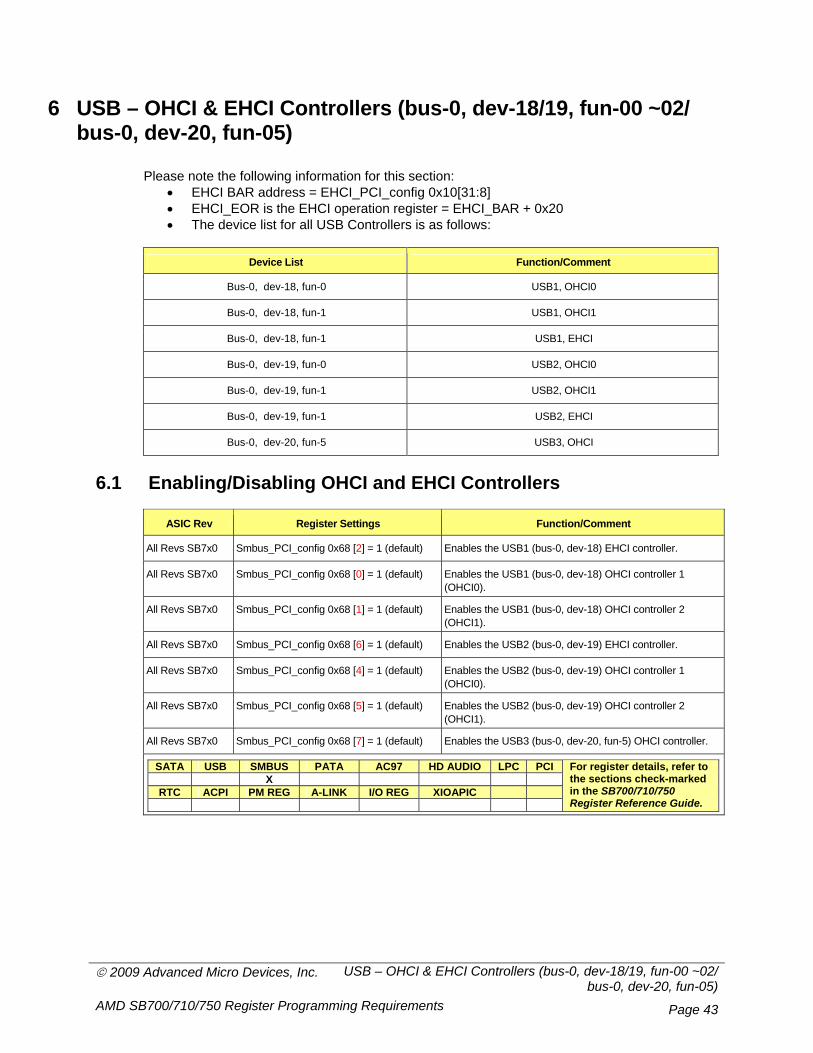
© 2009 Advanced Micro Devices, Inc. USB – OHCI & EHCI Controllers (bus-0, dev-18/19, fun-00 ~02/ bus-0, dev-20, fun-05)
AMD SB700/710/750 Register Programming Requirements Page 43
6 USB – OHCI & EHCI Controllers (bus-0, dev-18/19, fun-00 ~02/ bus-0, dev-20, fun-05)
Please note the following information for this section: • EHCI BAR address = EHCI_PCI_config 0x10[31:8] • EHCI_EOR is the EHCI operation register = EHCI_BAR + 0x20 • The device list for all USB Controllers is as follows:
Device List Function/Comment
Bus-0, dev-18, fun-0 USB1, OHCI0
Bus-0, dev-18, fun-1 USB1, OHCI1
Bus-0, dev-18, fun-1 USB1, EHCI
Bus-0, dev-19, fun-0 USB2, OHCI0
Bus-0, dev-19, fun-1 USB2, OHCI1
Bus-0, dev-19, fun-1 USB2, EHCI
Bus-0, dev-20, fun-5 USB3, OHCI
6.1 Enabling/Disabling OHCI and EHCI Controllers
ASIC Rev Register Settings Function/Comment
All Revs SB7x0 Smbus_PCI_config 0x68 [2] = 1 (default) Enables the USB1 (bus-0, dev-18) EHCI controller.
All Revs SB7x0 Smbus_PCI_config 0x68 [0] = 1 (default) Enables the USB1 (bus-0, dev-18) OHCI controller 1 (OHCI0).
All Revs SB7x0 Smbus_PCI_config 0x68 [1] = 1 (default) Enables the USB1 (bus-0, dev-18) OHCI controller 2 (OHCI1).
All Revs SB7x0 Smbus_PCI_config 0x68 [6] = 1 (default) Enables the USB2 (bus-0, dev-19) EHCI controller.
All Revs SB7x0 Smbus_PCI_config 0x68 [4] = 1 (default) Enables the USB2 (bus-0, dev-19) OHCI controller 1 (OHCI0).
All Revs SB7x0 Smbus_PCI_config 0x68 [5] = 1 (default) Enables the USB2 (bus-0, dev-19) OHCI controller 2 (OHCI1).
All Revs SB7x0 Smbus_PCI_config 0x68 [7] = 1 (default) Enables the USB3 (bus-0, dev-20, fun-5) OHCI controller.
SATA USB SMBUS PATA AC97 HD AUDIO LPC PCI X
RTC ACPI PM REG A-LINK I/O REG XIOAPIC
For register details, refer to the sections check-marked in the SB700/710/750 Register Reference Guide.
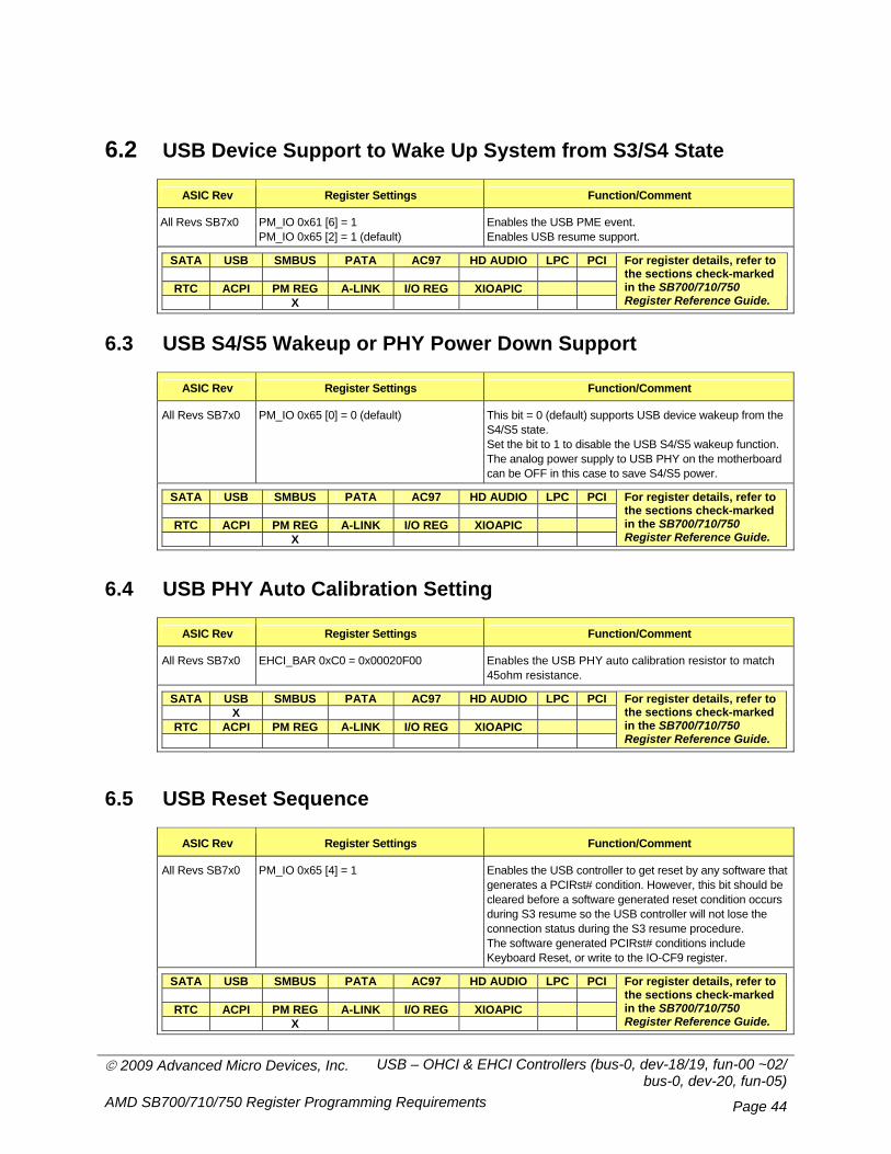
© 2009 Advanced Micro Devices, Inc. USB – OHCI & EHCI Controllers (bus-0, dev-18/19, fun-00 ~02/ bus-0, dev-20, fun-05)
AMD SB700/710/750 Register Programming Requirements Page 44
6.2 USB Device Support to Wake Up System from S3/S4 State
ASIC Rev Register Settings Function/Comment
All Revs SB7x0 PM_IO 0x61 [6] = 1 PM_IO 0x65 [2] = 1 (default)
Enables the USB PME event. Enables USB resume support.
SATA USB SMBUS PATA AC97 HD AUDIO LPC PCI
RTC ACPI PM REG A-LINK I/O REG XIOAPIC X
For register details, refer to the sections check-marked in the SB700/710/750 Register Reference Guide.
6.3 USB S4/S5 Wakeup or PHY Power Down Support
ASIC Rev Register Settings Function/Comment
All Revs SB7x0 PM_IO 0x65 [0] = 0 (default)
This bit = 0 (default) supports USB device wakeup from the S4/S5 state. Set the bit to 1 to disable the USB S4/S5 wakeup function. The analog power supply to USB PHY on the motherboard can be OFF in this case to save S4/S5 power.
SATA USB SMBUS PATA AC97 HD AUDIO LPC PCI
RTC ACPI PM REG A-LINK I/O REG XIOAPIC X
For register details, refer to the sections check-marked in the SB700/710/750 Register Reference Guide.
6.4 USB PHY Auto Calibration Setting
ASIC Rev Register Settings Function/Comment
All Revs SB7x0 EHCI_BAR 0xC0 = 0x00020F00 Enables the USB PHY auto calibration resistor to match 45ohm resistance.
SATA USB SMBUS PATA AC97 HD AUDIO LPC PCI X
RTC ACPI PM REG A-LINK I/O REG XIOAPIC
For register details, refer to the sections check-marked in the SB700/710/750 Register Reference Guide.
6.5 USB Reset Sequence
ASIC Rev Register Settings Function/Comment
All Revs SB7x0 PM_IO 0x65 [4] = 1
Enables the USB controller to get reset by any software that generates a PCIRst# condition. However, this bit should be cleared before a software generated reset condition occurs during S3 resume so the USB controller will not lose the connection status during the S3 resume procedure. The software generated PCIRst# conditions include Keyboard Reset, or write to the IO-CF9 register.
SATA USB SMBUS PATA AC97 HD AUDIO LPC PCI
RTC ACPI PM REG A-LINK I/O REG XIOAPIC X
For register details, refer to the sections check-marked in the SB700/710/750 Register Reference Guide.
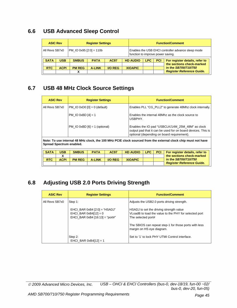
© 2009 Advanced Micro Devices, Inc. USB – OHCI & EHCI Controllers (bus-0, dev-18/19, fun-00 ~02/ bus-0, dev-20, fun-05)
AMD SB700/710/750 Register Programming Requirements Page 45
6.6 USB Advanced Sleep Control
ASIC Rev Register Settings Function/Comment
All Revs SB7x0 PM_IO 0x95 [2:0] = 110b Enables the USB EHCI controller advance sleep mode function to improve power saving.
SATA USB SMBUS PATA AC97 HD AUDIO LPC PCI
RTC ACPI PM REG A-LINK I/O REG XIOAPIC X
For register details, refer to the sections check-marked in the SB700/710/750 Register Reference Guide.
6.7 USB 48 MHz Clock Source Settings
ASIC Rev Register Settings Function/Comment
All Revs SB7x0 PM_IO 0xD0 [0] = 0 (default) PM_IO 0xBD [4] = 1 PM_IO 0xBD [6] = 1 (optional)
Enables PLL “CG_PLL2” to generate 48Mhz clock internally. Enables the internal 48Mhz as the clock source to USBPHY. Enables the IO pad “USBCLK/14M_25M_48M” as clock output pad that it can be used for on board devices. This is optional (depending on board requirement).
Note: To use internal 48 MHz clock, the 100 MHz PCIE clock sourced from the external clock chip must not have Spread Spectrum enabled.
SATA USB SMBUS PATA AC97 HD AUDIO LPC PCI X
RTC ACPI PM REG A-LINK I/O REG XIOAPIC
For register details, refer to the sections check-marked in the SB700/710/750 Register Reference Guide.
6.8 Adjusting USB 2.0 Ports Driving Strength
ASIC Rev Register Settings Function/Comment
All Revs SB7x0 Step 1: EHCI_BAR 0xB4 [2:0] = “HSADJ” EHCI_BAR 0xB4[12] = 0 EHCI_BAR 0xB4 [16:13] = “port#” Step 2: EHCI_BAR 0xB4[12] = 1
Adjusts the USB2.0 ports driving strength. HSADJ to set the driving strength value VLoadB to load the value to the PHY for selected port The selected port# The SBIOS can repeat step-1 for those ports with less margin on HS eye diagram. Set to ‘1’ to lock PHY UTMI Control interface.
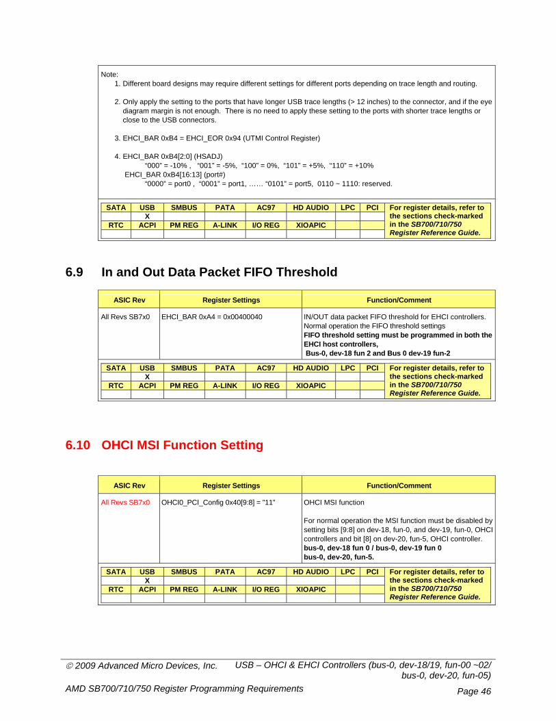
© 2009 Advanced Micro Devices, Inc. USB – OHCI & EHCI Controllers (bus-0, dev-18/19, fun-00 ~02/ bus-0, dev-20, fun-05)
AMD SB700/710/750 Register Programming Requirements Page 46
Note: 1. Different board designs may require different settings for different ports depending on trace length and routing. 2. Only apply the setting to the ports that have longer USB trace lengths (> 12 inches) to the connector, and if the eye
diagram margin is not enough. There is no need to apply these setting to the ports with shorter trace lengths or close to the USB connectors.
3. EHCI_BAR 0xB4 = EHCI_EOR 0x94 (UTMI Control Register) 4. EHCI_BAR 0xB4[2:0] (HSADJ) “000” = -10% , “001” = -5%, “100” = 0%, “101” = +5%, “110” = +10% EHCI_BAR 0xB4[16:13] (port#) “0000” = port0 , “0001” = port1, …… “0101” = port5, 0110 ~ 1110: reserved.
SATA USB SMBUS PATA AC97 HD AUDIO LPC PCI X
RTC ACPI PM REG A-LINK I/O REG XIOAPIC
For register details, refer to the sections check-marked in the SB700/710/750 Register Reference Guide.
6.9 In and Out Data Packet FIFO Threshold
ASIC Rev Register Settings Function/Comment
All Revs SB7x0 EHCI_BAR 0xA4 = 0x00400040
IN/OUT data packet FIFO threshold for EHCI controllers. Normal operation the FIFO threshold settings FIFO threshold setting must be programmed in both the EHCI host controllers, Bus-0, dev-18 fun 2 and Bus 0 dev-19 fun-2
SATA USB SMBUS PATA AC97 HD AUDIO LPC PCI X
RTC ACPI PM REG A-LINK I/O REG XIOAPIC
For register details, refer to the sections check-marked in the SB700/710/750 Register Reference Guide.
6.10 OHCI MSI Function Setting
ASIC Rev Register Settings Function/Comment
All Revs SB7x0 OHCI0_PCI_Config 0x40[9:8] = ”11”
OHCI MSI function For normal operation the MSI function must be disabled by setting bits [9:8] on dev-18, fun-0, and dev-19, fun-0, OHCI controllers and bit [8] on dev-20, fun-5, OHCI controller. bus-0, dev-18 fun 0 / bus-0, dev-19 fun 0 bus-0, dev-20, fun-5.
SATA USB SMBUS PATA AC97 HD AUDIO LPC PCI X
RTC ACPI PM REG A-LINK I/O REG XIOAPIC
For register details, refer to the sections check-marked in the SB700/710/750 Register Reference Guide.
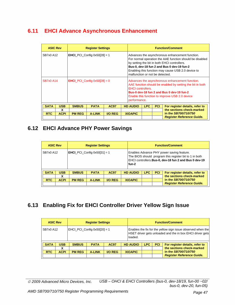
© 2009 Advanced Micro Devices, Inc. USB – OHCI & EHCI Controllers (bus-0, dev-18/19, fun-00 ~02/ bus-0, dev-20, fun-05)
AMD SB700/710/750 Register Programming Requirements Page 47
6.11 EHCI Advance Asynchronous Enhancement
ASIC Rev Register Settings Function/Comment
SB7x0 A12 EHCI_PCI_Config 0x50[28] = 1
Advances the asynchronous enhancement function. For normal operation the AAE function should be disabled by setting the bit in both EHCI controllers. Bus-0, dev-18 fun 2 and Bus 0 dev-19 fun-2 Enabling this function may cause USB 2.0 device to malfunction or not be detected.
SB7x0 A14 EHCI_PCI_Config 0x50[28] = 0
Advances the asynchronous enhancement function. AAE function should be enabled by setting the bit in both EHCI controllers. Bus-0 dev-18 fun 2 and Bus 0 dev-19 fun-2 Enable this function to improve USB 2.0 device performance.
SATA USB SMBUS PATA AC97 HD AUDIO LPC PCI X
RTC ACPI PM REG A-LINK I/O REG XIOAPIC
For register details, refer to the sections check-marked in the SB700/710/750 Register Reference Guide.
6.12 EHCI Advance PHY Power Savings
ASIC Rev Register Settings Function/Comment
SB7x0 A12 EHCI_PCI_Config 0x50[31] = 1
Enables Advance PHY power saving feature. The BIOS should program this register bit to 1 in both EHCI controllers.Bus-0, dev-18 fun 2 and Bus 0 dev-19 fun-2
SATA USB SMBUS PATA AC97 HD AUDIO LPC PCI X
RTC ACPI PM REG A-LINK I/O REG XIOAPIC
For register details, refer to the sections check-marked in the SB700/710/750 Register Reference Guide.
6.13 Enabling Fix for EHCI Controller Driver Yellow Sign Issue
ASIC Rev Register Settings Function/Comment
SB7x0 A12 EHCI_PCI_Config 0x50[20] = 1
Enables the fix for the yellow sign issue observed when the HSET driver gets unloaded and the in box EHCI driver gets loaded.
SATA USB SMBUS PATA AC97 HD AUDIO LPC PCI X
RTC ACPI PM REG A-LINK I/O REG XIOAPIC
For register details, refer to the sections check-marked in the SB700/710/750 Register Reference Guide.
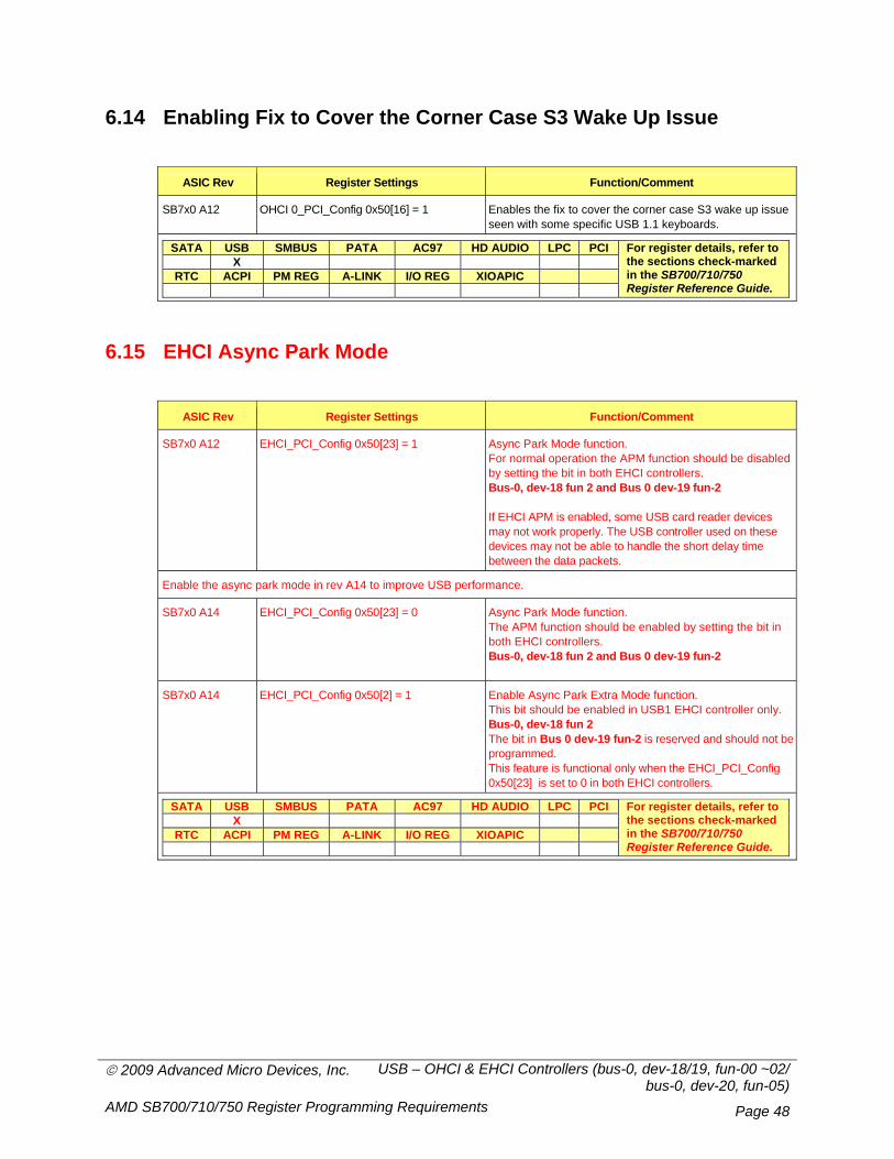
© 2009 Advanced Micro Devices, Inc. USB – OHCI & EHCI Controllers (bus-0, dev-18/19, fun-00 ~02/ bus-0, dev-20, fun-05)
AMD SB700/710/750 Register Programming Requirements Page 48
6.14 Enabling Fix to Cover the Corner Case S3 Wake Up Issue
ASIC Rev Register Settings Function/Comment
SB7x0 A12 OHCI 0_PCI_Config 0x50[16] = 1 Enables the fix to cover the corner case S3 wake up issue seen with some specific USB 1.1 keyboards.
SATA USB SMBUS PATA AC97 HD AUDIO LPC PCI X
RTC ACPI PM REG A-LINK I/O REG XIOAPIC
For register details, refer to the sections check-marked in the SB700/710/750 Register Reference Guide.
6.15 EHCI Async Park Mode
ASIC Rev Register Settings Function/Comment
SB7x0 A12 EHCI_PCI_Config 0x50[23] = 1
Async Park Mode function. For normal operation the APM function should be disabled by setting the bit in both EHCI controllers. Bus-0, dev-18 fun 2 and Bus 0 dev-19 fun-2 If EHCI APM is enabled, some USB card reader devices may not work properly. The USB controller used on these devices may not be able to handle the short delay time between the data packets.
Enable the async park mode in rev A14 to improve USB performance.
SB7x0 A14 EHCI_PCI_Config 0x50[23] = 0 Async Park Mode function. The APM function should be enabled by setting the bit in both EHCI controllers. Bus-0, dev-18 fun 2 and Bus 0 dev-19 fun-2
SB7x0 A14 EHCI_PCI_Config 0x50[2] = 1
Enable Async Park Extra Mode function. This bit should be enabled in USB1 EHCI controller only. Bus-0, dev-18 fun 2 The bit in Bus 0 dev-19 fun-2 is reserved and should not be programmed. This feature is functional only when the EHCI_PCI_Config 0x50[23] is set to 0 in both EHCI controllers.
SATA USB SMBUS PATA AC97 HD AUDIO LPC PCI X
RTC ACPI PM REG A-LINK I/O REG XIOAPIC
For register details, refer to the sections check-marked in the SB700/710/750 Register Reference Guide.
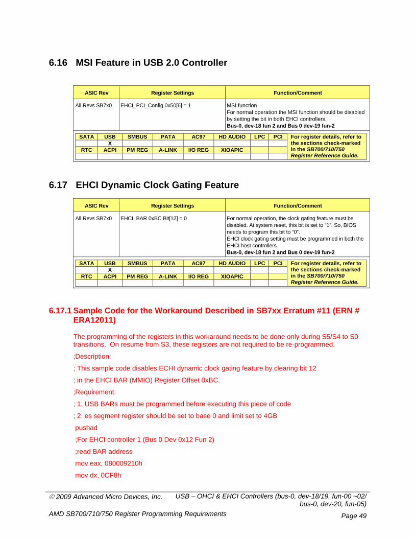
© 2009 Advanced Micro Devices, Inc. USB – OHCI & EHCI Controllers (bus-0, dev-18/19, fun-00 ~02/ bus-0, dev-20, fun-05)
AMD SB700/710/750 Register Programming Requirements Page 49
6.16 MSI Feature in USB 2.0 Controller
ASIC Rev Register Settings Function/Comment
All Revs SB7x0 EHCI_PCI_Config 0x50[6] = 1
MSI function For normal operation the MSI function should be disabled by setting the bit in both EHCI controllers. Bus-0, dev-18 fun 2 and Bus 0 dev-19 fun-2
SATA USB SMBUS PATA AC97 HD AUDIO LPC PCI X
RTC ACPI PM REG A-LINK I/O REG XIOAPIC
For register details, refer to the sections check-marked in the SB700/710/750 Register Reference Guide.
6.17 EHCI Dynamic Clock Gating Feature
ASIC Rev Register Settings Function/Comment
All Revs SB7x0 EHCI_BAR 0xBC Bit[12] = 0
For normal operation, the clock gating feature must be disabled. At system reset, this bit is set to “1”. So, BIOS needs to program this bit to “0”. EHCI clock gating setting must be programmed in both the EHCI host controllers. Bus-0, dev-18 fun 2 and Bus 0 dev-19 fun-2
SATA USB SMBUS PATA AC97 HD AUDIO LPC PCI X
RTC ACPI PM REG A-LINK I/O REG XIOAPIC
For register details, refer to the sections check-marked in the SB700/710/750 Register Reference Guide.
6.17.1 Sample Code for the Workaround Described in SB7xx Erratum #11 (ERN # ERA12011)
The programming of the registers in this workaround needs to be done only during S5/S4 to S0 transitions. On resume from S3, these registers are not required to be re-programmed.
;Description:
; This sample code disables ECHI dynamic clock gating feature by clearing bit 12
; in the EHCI BAR (MMIO) Register Offset 0xBC.
;Requirement:
; 1. USB BARs must be programmed before executing this piece of code
; 2. es segment register should be set to base 0 and limit set to 4GB
pushad
;For EHCI controller 1 (Bus 0 Dev 0x12 Fun 2)
;read BAR address
mov eax, 080009210h
mov dx, 0CF8h
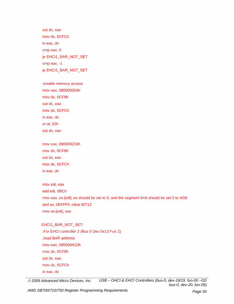
© 2009 Advanced Micro Devices, Inc. USB – OHCI & EHCI Controllers (bus-0, dev-18/19, fun-00 ~02/ bus-0, dev-20, fun-05)
AMD SB700/710/750 Register Programming Requirements Page 50
out dx, eax
mov dx, 0CFCh
in eax, dx
cmp eax, 0
je EHCI1_BAR_NOT_SET
cmp eax, -1
je EHCI1_BAR_NOT_SET
;enable memory access
mov eax, 080009204h
mov dx, 0CF8h
out dx, eax
mov dx, 0CFCh
in eax, dx
or al, 02h
out dx, eax
mov eax, 080009210h
mov dx, 0CF8h
out dx, eax
mov dx, 0CFCh
in eax, dx
mov edi, eax
add edi, 0BCh
mov eax, es:[edi] ;es should be set to 0, and the segment limit should be set 0 to 4GB
and ax, 0EFFFh ;clear BIT12
mov es:[edi], eax
EHCI1_BAR_NOT_SET:
;For EHCI controller 2 (Bus 0 Dev 0x13 Fun 2)
;read BAR address
mov eax, 080009A10h
mov dx, 0CF8h
out dx, eax
mov dx, 0CFCh
in eax, dx

© 2009 Advanced Micro Devices, Inc. USB – OHCI & EHCI Controllers (bus-0, dev-18/19, fun-00 ~02/ bus-0, dev-20, fun-05)
AMD SB700/710/750 Register Programming Requirements Page 51
cmp eax, 0
je EHCI2_BAR_NOT_SET
cmp eax, -1
je EHCI2_BAR_NOT_SET
;enable memory access
mov eax, 080009A04h
mov dx, 0CF8h
out dx, eax
mov dx, 0CFCh
in eax, dx
or al, 02h
out dx, eax
mov eax, 080009A10h
mov dx, 0CF8h
out dx, eax
mov dx, 0CFCh
in eax, dx
mov edi, eax
add edi, 0BCh
mov eax, es:[edi] ;es should be set to 0, and the segment limit should be set 0 to 4GB
and ax, 0EFFFh ;clear BIT12
mov es:[edi], eax
EHCI2_BAR_NOT_SET:
popad
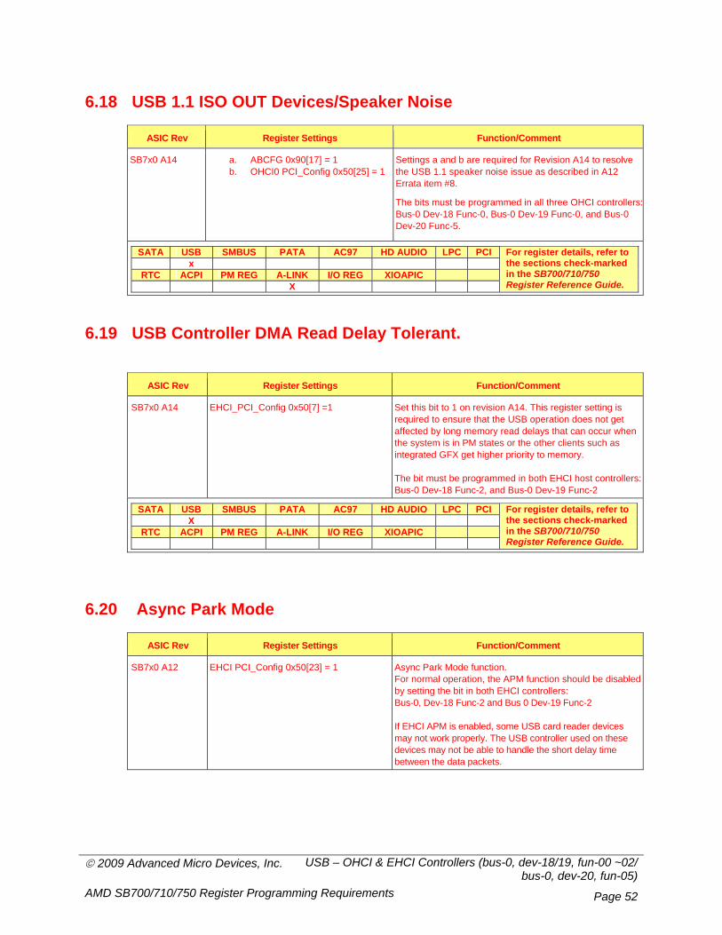
© 2009 Advanced Micro Devices, Inc. USB – OHCI & EHCI Controllers (bus-0, dev-18/19, fun-00 ~02/ bus-0, dev-20, fun-05)
AMD SB700/710/750 Register Programming Requirements Page 52
6.18 USB 1.1 ISO OUT Devices/Speaker Noise
ASIC Rev Register Settings Function/Comment
SB7x0 A14
a. ABCFG 0x90[17] = 1 b. OHCI0 PCI_Config 0x50[25] = 1
Settings a and b are required for Revision A14 to resolve the USB 1.1 speaker noise issue as described in A12 Errata item #8.
The bits must be programmed in all three OHCI controllers:Bus-0 Dev-18 Func-0, Bus-0 Dev-19 Func-0, and Bus-0 Dev-20 Func-5.
SATA USB SMBUS PATA AC97 HD AUDIO LPC PCI x
RTC ACPI PM REG A-LINK I/O REG XIOAPIC X
For register details, refer to the sections check-marked in the SB700/710/750 Register Reference Guide.
6.19 USB Controller DMA Read Delay Tolerant.
ASIC Rev Register Settings Function/Comment
SB7x0 A14
EHCI_PCI_Config 0x50[7] =1
Set this bit to 1 on revision A14. This register setting is required to ensure that the USB operation does not get affected by long memory read delays that can occur when the system is in PM states or the other clients such as integrated GFX get higher priority to memory. The bit must be programmed in both EHCI host controllers:Bus-0 Dev-18 Func-2, and Bus-0 Dev-19 Func-2
SATA USB SMBUS PATA AC97 HD AUDIO LPC PCI X
RTC ACPI PM REG A-LINK I/O REG XIOAPIC
For register details, refer to the sections check-marked in the SB700/710/750 Register Reference Guide.
6.20 Async Park Mode
ASIC Rev Register Settings Function/Comment
SB7x0 A12
EHCI PCI_Config 0x50[23] = 1
Async Park Mode function. For normal operation, the APM function should be disabled by setting the bit in both EHCI controllers: Bus-0, Dev-18 Func-2 and Bus 0 Dev-19 Func-2 If EHCI APM is enabled, some USB card reader devices may not work properly. The USB controller used on these devices may not be able to handle the short delay time between the data packets.
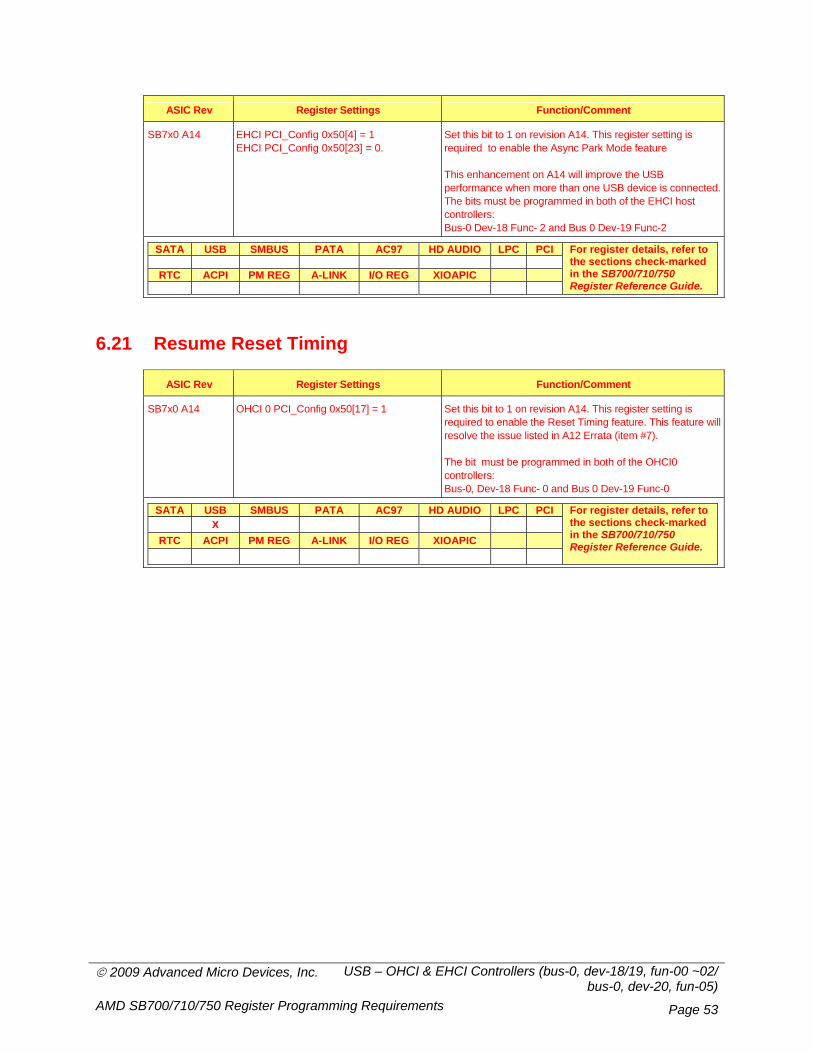
© 2009 Advanced Micro Devices, Inc. USB – OHCI & EHCI Controllers (bus-0, dev-18/19, fun-00 ~02/ bus-0, dev-20, fun-05)
AMD SB700/710/750 Register Programming Requirements Page 53
ASIC Rev Register Settings Function/Comment
SB7x0 A14
EHCI PCI_Config 0x50[4] = 1 EHCI PCI_Config 0x50[23] = 0.
Set this bit to 1 on revision A14. This register setting is required to enable the Async Park Mode feature This enhancement on A14 will improve the USB performance when more than one USB device is connected.The bits must be programmed in both of the EHCI host controllers: Bus-0 Dev-18 Func- 2 and Bus 0 Dev-19 Func-2
SATA USB SMBUS PATA AC97 HD AUDIO LPC PCI
RTC ACPI PM REG A-LINK I/O REG XIOAPIC
For register details, refer to the sections check-marked in the SB700/710/750 Register Reference Guide.
6.21 Resume Reset Timing
ASIC Rev Register Settings Function/Comment
SB7x0 A14
OHCI 0 PCI_Config 0x50[17] = 1
Set this bit to 1 on revision A14. This register setting is required to enable the Reset Timing feature. This feature will resolve the issue listed in A12 Errata (item #7). The bit must be programmed in both of the OHCI0 controllers: Bus-0, Dev-18 Func- 0 and Bus 0 Dev-19 Func-0
SATA USB SMBUS PATA AC97 HD AUDIO LPC PCI X
RTC ACPI PM REG A-LINK I/O REG XIOAPIC
For register details, refer to the sections check-marked in the SB700/710/750 Register Reference Guide.
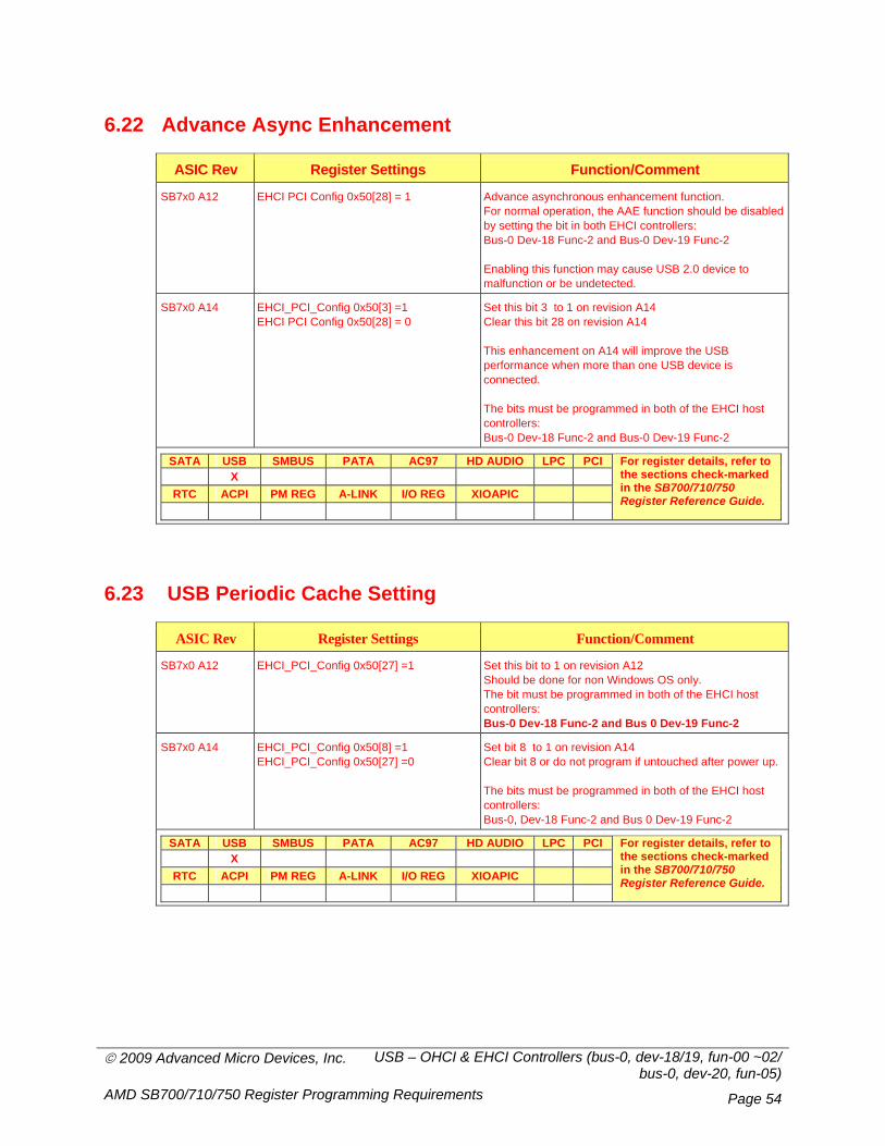
© 2009 Advanced Micro Devices, Inc. USB – OHCI & EHCI Controllers (bus-0, dev-18/19, fun-00 ~02/ bus-0, dev-20, fun-05)
AMD SB700/710/750 Register Programming Requirements Page 54
6.22 Advance Async Enhancement
ASIC Rev Register Settings Function/Comment
SB7x0 A12 EHCI PCI Config 0x50[28] = 1
Advance asynchronous enhancement function. For normal operation, the AAE function should be disabled by setting the bit in both EHCI controllers: Bus-0 Dev-18 Func-2 and Bus-0 Dev-19 Func-2 Enabling this function may cause USB 2.0 device to malfunction or be undetected.
SB7x0 A14
EHCI_PCI_Config 0x50[3] =1 EHCI PCI Config 0x50[28] = 0
Set this bit 3 to 1 on revision A14 Clear this bit 28 on revision A14 This enhancement on A14 will improve the USB performance when more than one USB device is connected. The bits must be programmed in both of the EHCI host controllers: Bus-0 Dev-18 Func-2 and Bus-0 Dev-19 Func-2
SATA USB SMBUS PATA AC97 HD AUDIO LPC PCI X
RTC ACPI PM REG A-LINK I/O REG XIOAPIC
For register details, refer to the sections check-marked in the SB700/710/750 Register Reference Guide.
6.23 USB Periodic Cache Setting
ASIC Rev Register Settings Function/Comment
SB7x0 A12
EHCI_PCI_Config 0x50[27] =1
Set this bit to 1 on revision A12 Should be done for non Windows OS only. The bit must be programmed in both of the EHCI host controllers: Bus-0 Dev-18 Func-2 and Bus 0 Dev-19 Func-2
SB7x0 A14
EHCI_PCI_Config 0x50[8] =1 EHCI_PCI_Config 0x50[27] =0
Set bit 8 to 1 on revision A14 Clear bit 8 or do not program if untouched after power up. The bits must be programmed in both of the EHCI host controllers: Bus-0, Dev-18 Func-2 and Bus 0 Dev-19 Func-2
SATA USB SMBUS PATA AC97 HD AUDIO LPC PCI X
RTC ACPI PM REG A-LINK I/O REG XIOAPIC
For register details, refer to the sections check-marked in the SB700/710/750 Register Reference Guide.
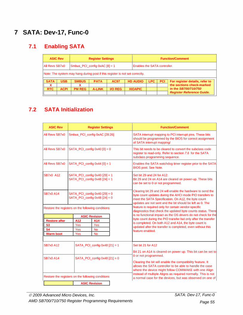
© 2009 Advanced Micro Devices, Inc. SATA: Dev-17, Func-0 AMD SB700/710/750 Register Programming Requirements Page 55
7 SATA: Dev-17, Func-0
7.1 Enabling SATA
ASIC Rev Register Settings Function/Comment
All Revs SB7x0 Smbus_PCI_config 0xAC [8] = 1 Enables the SATA controller.
Note: The system may hang during post if this register is not set correctly.
SATA USB SMBUS PATA AC97 HD AUDIO LPC PCI X X
RTC ACPI PM REG A-LINK I/O REG XIOAPIC
For register details, refer to the sections check-marked in the SB700/710/750 Register Reference Guide.
7.2 SATA Initialization
ASIC Rev Register Settings Function/Comment
All Revs SB7x0 Smbus_PCI_config 0xAC [28:26]
SATA interrupt mapping to PCI interrupt pins. These bits should be programmed by the BIOS for correct assignment of SATA interrupt mapping/
All Revs SB7x0 SATA_PCI_config 0x40 [0] = 0 This bit needs to be cleared to convert the subclass code register to read-only. Refer to section 7.6 for the SATA subclass programming sequence.
All Revs SB7x0 SATA_PCI_config 0x44 [0] = 1 Enables the SATA watchdog timer register prior to the SATA BIOS post. See Note.
SB7x0 A12
SATA_PCI_config 0x40 [29] = 1 SATA_PCI_config 0x48 [24] = 1
SB7x0 A14
SATA_PCI_config 0x40 [29] = 0 SATA_PCI_config 0x48 [24] = 0
Restore the registers on the following conditions:
ASIC Revision Restore after A12 A14 S3 Yes Yes S4 Yes No Warm boot Yes No
Set bit 29 and 24 for A12. Bit 29 and 24 on A14 are cleared on power-up. These bits can be set to 0 or not programmed. Clearing bit 29 and 24 will enable the hardware to send the byte count updates during the AHCI mode PIO transfers to meet the SATA Specification. On A12, the byte count updates are not sent and the bit should be left as 0. The feature is required only for certain vendor-specific diagnostics that check the updated byte counts status. Thereis no functional impact as the OS drivers do not check for thebyte count during the PIO transfer but only after the transfer is completed. On both A12 and A14, the byte count is updated after the transfer is completed, even without this feature enabled.
SB7x0 A12 SATA_PCI_config 0x48 [21] = 1
SB7x0 A14
SATA_PCI_config 0x48 [21] = 0
Restore the registers on the following conditions
ASIC Revision
Set bit 21 for A12
Bit 21 on A14 is cleared on power up. This bit can be set to 0 or not programmed.
Clearing the bit will enable the compatibility feature. It allows the SATA controller to be able to handle the case where the device might follow COMWAKE with one Align instead of multiple Aligns as required normally. This is not a normal case for the devices, but was observed on one of
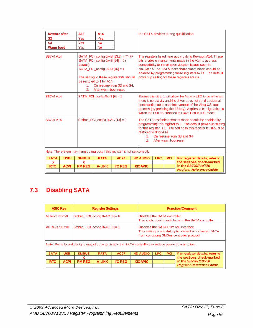
© 2009 Advanced Micro Devices, Inc. SATA: Dev-17, Func-0 AMD SB700/710/750 Register Programming Requirements Page 56
the SATA devices during qualification.
Restore after A12 A14 S3 Yes Yes S4 Yes No Warm boot Yes No
SB7x0 A14
SATA_PCI_config 0x48 [13:7] = 7’h7F SATA_PCI_config 0x48 [14] = 0 ( default) SATA_PCI_config 0x48 [15] = 1 The setting to these register bits should be restored to 1 for A14
1. On resume from S3 and S4. 2. After warm boot reset.
The registers listed here apply only to Revision A14. These bits enable enhancements made in the A14 to address compatibility or minor spec violation issues seen in simulation. The SATA test/enhancement mode should be enabled by programming these registers to 1s. The default power-up setting for these registers are 0s.
SB7x0 A14
SATA_PCI_config 0x48 [6] = 1 Setting this bit to 1 will allow the Activity LED to go off when there is no activity and the driver does not send additional commands due to user intervention of the Vista OS boot process (by pressing the F8 key). Applies to configuration in which the ODD is attached to Slave Port in IDE mode.
SB7x0 A14
Smbus_PCI_config 0xAC [13] = 0 The SATA test/enhancement mode should be enabled by programming this register to 0. The default power-up setting for this register is 1. The setting to this register bit should be restored to 0 for A14
1. On resume from S3 and S4 2. After warm boot reset
..
Note: The system may hang during post if this register is not set correctly.
SATA USB SMBUS PATA AC97 HD AUDIO LPC PCI X X
RTC ACPI PM REG A-LINK I/O REG XIOAPIC
For register details, refer to the sections check-marked in the SB700/710/750 Register Reference Guide.
7.3 Disabling SATA
ASIC Rev Register Settings Function/Comment
All Revs SB7x0 Smbus_PCI_config 0xAC [8] = 0 Disables the SATA controller. This shuts down most clocks in the SATA controller.
All Revs SB7x0 Smbus_PCI_config 0xAC [9] = 1 Disables the SATA PHY I2C interface. This setting is mandatory to prevent un-powered SATA from corrupting SMBus controller protocol.
Note: Some board designs may choose to disable the SATA controllers to reduce power consumption.
SATA USB SMBUS PATA AC97 HD AUDIO LPC PCI X
RTC ACPI PM REG A-LINK I/O REG XIOAPIC
For register details, refer to the sections check-marked in the SB700/710/750 Register Reference Guide.
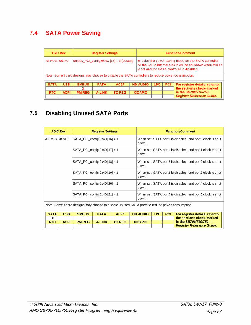
© 2009 Advanced Micro Devices, Inc. SATA: Dev-17, Func-0 AMD SB700/710/750 Register Programming Requirements Page 57
7.4 SATA Power Saving
ASIC Rev Register Settings Function/Comment
All Revs SB7x0 Smbus_PCI_config 0xAC [13] = 1 (default) Enables the power saving mode for the SATA controller. All the SATA Internal clocks will be shutdown when this bit is set and the SATA controller is disabled.
Note: Some board designs may choose to disable the SATA controllers to reduce power consumption.
SATA USB SMBUS PATA AC97 HD AUDIO LPC PCI X
RTC ACPI PM REG A-LINK I/O REG XIOAPIC
For register details, refer to the sections check-marked in the SB700/710/750 Register Reference Guide.
7.5 Disabling Unused SATA Ports
ASIC Rev Register Settings Function/Comment
SATA_PCI_config 0x40 [16] = 1 When set, SATA port0 is disabled, and port0 clock is shut down.
SATA_PCI_config 0x40 [17] = 1 When set, SATA port1 is disabled, and port1 clock is shut down.
SATA_PCI_config 0x40 [18] = 1 When set, SATA port2 is disabled, and port2 clock is shut down.
SATA_PCI_config 0x40 [19] = 1 When set, SATA port3 is disabled, and port3 clock is shut down.
SATA_PCI_config 0x40 [20] = 1 When set, SATA port4 is disabled, and port4 clock is shut down.
All Revs SB7x0
SATA_PCI_config 0x40 [21] = 1 When set, SATA port5 is disabled, and port5 clock is shut down.
Note: Some board designs may choose to disable unused SATA ports to reduce power consumption.
SATA USB SMBUS PATA AC97 HD AUDIO LPC PCI X
RTC ACPI PM REG A-LINK I/O REG XIOAPIC
For register details, refer to the sections check-marked in the SB700/710/750 Register Reference Guide.
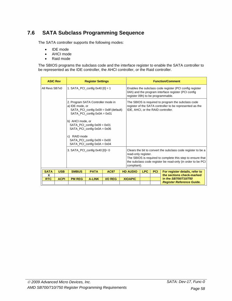
© 2009 Advanced Micro Devices, Inc. SATA: Dev-17, Func-0 AMD SB700/710/750 Register Programming Requirements Page 58
7.6 SATA Subclass Programming Sequence
The SATA controller supports the following modes:
• IDE mode • AHCI mode • Raid mode
The SBIOS programs the subclass code and the interface register to enable the SATA controller to be represented as the IDE controller, the AHCI controller, or the Raid controller.
ASIC Rev Register Settings Function/Comment
1. SATA_PCI_config 0x40 [0] = 1 Enables the subclass code register (PCI config register 0Ah) and the program interface register (PCI config register 09h) to be programmable.
2. Program SATA Controller mode in a) IDE mode, or SATA_PCI_config 0x09 = 0x8f (default) SATA_PCI_config 0x0A = 0x01 b) AHCI mode, or SATA_PCI_config 0x09 = 0x01 SATA_PCI_config 0x0A = 0x06 c) RAID mode SATA_PCI_config 0x09 = 0x00 SATA_PCI_config 0x0A = 0x04
The SBIOS is required to program the subclass code register of the SATA controller to be represented as the IDE, AHCI, or the RAID controller.
All Revs SB7x0
3. SATA_PCI_config 0x40 [0]= 0 Clears the bit to convert the subclass code register to be a read-only register. The SBIOS is required to complete this step to ensure that the subclass code register be read-only (in order to be PCI compliant).
SATA USB SMBUS PATA AC97 HD AUDIO LPC PCI X
RTC ACPI PM REG A-LINK I/O REG XIOAPIC
For register details, refer to the sections check-marked in the SB700/710/750 Register Reference Guide.
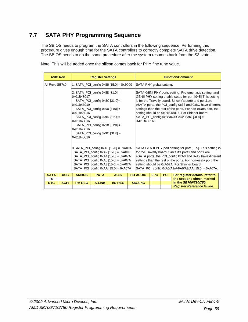
© 2009 Advanced Micro Devices, Inc. SATA: Dev-17, Func-0 AMD SB700/710/750 Register Programming Requirements Page 59
7.7 SATA PHY Programming Sequence
The SBIOS needs to program the SATA controllers in the following sequence. Performing this procedure gives enough time for the SATA controllers to correctly complete SATA drive detection. The SBIOS needs to do the same procedure after the system resumes back from the S3 state. Note: This will be added once the silicon comes back for PHY fine tune value.
ASIC Rev Register Settings Function/Comment
1. SATA_PCI_config 0x86 [15:0] = 0x2C00 SATA PHY global setting.
2. SATA_PCI_config 0x88 [31:0] = 0x01B48017 SATA_PCI_config 0x8C [31:0]= 0x01B48019 SATA_PCI_config 0x90 [31:0] = 0x01B48016 SATA_PCI_config 0x94 [31:0] = 0x01B48016 SATA_PCI_config 0x98 [31:0] = 0x01B48016 SATA_PCI_config 0x9C [31:0] = 0x01B48016
SATA GENI PHY ports setting, Pre-emphasis setting, and GENII PHY setting enable setup for port [0~5] This setting is for the Travelly board. Since it’s port0 and port1are eSATA ports, the PCI_config 0x88 and 0x8C have different settings than the rest of the ports. For non-eSata port, the setting should be 0x01B48016. For Shinner board, SATA_PCI_config 0x88/8C/90/94/98/9C [31:0] = 0x01B48016.
All Revs SB7x0
3.SATA_PCI_config 0xA0 [15:0] = 0xA09A SATA_PCI_config 0xA2 [15:0] = 0xA09F SATA_PCI_config 0xA4 [15:0] = 0xA07A SATA_PCI_config 0xA6 [15:0] = 0xA07A SATA_PCI_config 0xA8 [15:0] = 0xA07A SATA_PCI_config 0xAA [15:0] = 0xA07A
SATA GEN II PHY port setting for port [0~5]. This setting is for the Travelly board. Since it’s port0 and port1 are eSATA ports, the PCI_config 0xA0 and 0xA2 have differentsettings than the rest of the ports. For non-esata port, the setting should be 0xA07A. For Shinner board, SATA_PCI_config 0xA0/A2/A4/A6/A8/AA [15:0] = 0xA07A.
SATA USB SMBUS PATA AC97 HD AUDIO LPC PCI X
RTC ACPI PM REG A-LINK I/O REG XIOAPIC
For register details, refer to the sections check-marked in the SB700/710/750 Register Reference Guide.
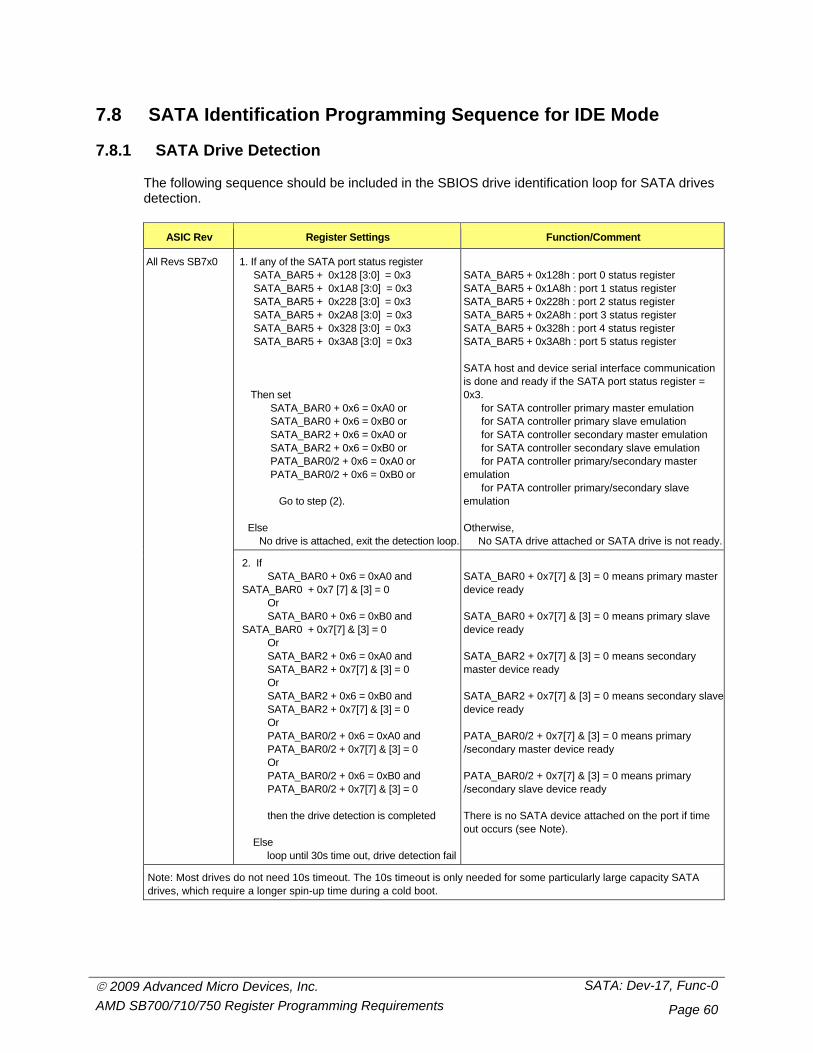
© 2009 Advanced Micro Devices, Inc. SATA: Dev-17, Func-0 AMD SB700/710/750 Register Programming Requirements Page 60
7.8 SATA Identification Programming Sequence for IDE Mode
7.8.1 SATA Drive Detection
The following sequence should be included in the SBIOS drive identification loop for SATA drives detection.
ASIC Rev Register Settings Function/Comment
1. If any of the SATA port status register SATA_BAR5 + 0x128 [3:0] = 0x3 SATA_BAR5 + 0x1A8 [3:0] = 0x3 SATA_BAR5 + 0x228 [3:0] = 0x3 SATA_BAR5 + 0x2A8 [3:0] = 0x3 SATA_BAR5 + 0x328 [3:0] = 0x3 SATA_BAR5 + 0x3A8 [3:0] = 0x3 Then set SATA_BAR0 + 0x6 = 0xA0 or SATA_BAR0 + 0x6 = 0xB0 or SATA_BAR2 + 0x6 = 0xA0 or SATA_BAR2 + 0x6 = 0xB0 or PATA_BAR0/2 + 0x6 = 0xA0 or PATA_BAR0/2 + 0x6 = 0xB0 or Go to step (2). Else No drive is attached, exit the detection loop.
SATA_BAR5 + 0x128h : port 0 status register SATA_BAR5 + 0x1A8h : port 1 status register SATA_BAR5 + 0x228h : port 2 status register SATA_BAR5 + 0x2A8h : port 3 status register SATA_BAR5 + 0x328h : port 4 status register SATA_BAR5 + 0x3A8h : port 5 status register SATA host and device serial interface communication is done and ready if the SATA port status register = 0x3. for SATA controller primary master emulation for SATA controller primary slave emulation for SATA controller secondary master emulation for SATA controller secondary slave emulation for PATA controller primary/secondary master emulation for PATA controller primary/secondary slave emulation Otherwise, No SATA drive attached or SATA drive is not ready.
All Revs SB7x0
2. If SATA_BAR0 + 0x6 = 0xA0 and SATA_BAR0 + 0x7 [7] & [3] = 0 Or SATA_BAR0 + 0x6 = 0xB0 and SATA_BAR0 + 0x7[7] & [3] = 0 Or SATA_BAR2 + 0x6 = 0xA0 and SATA_BAR2 + 0x7[7] & [3] = 0 Or SATA_BAR2 + 0x6 = 0xB0 and SATA_BAR2 + 0x7[7] & [3] = 0 Or PATA_BAR0/2 + 0x6 = 0xA0 and PATA_BAR0/2 + 0x7[7] & [3] = 0 Or PATA_BAR0/2 + 0x6 = 0xB0 and PATA_BAR0/2 + 0x7[7] & [3] = 0 then the drive detection is completed
Else loop until 30s time out, drive detection fail
SATA_BAR0 + 0x7[7] & [3] = 0 means primary master device ready SATA_BAR0 + 0x7[7] & [3] = 0 means primary slave device ready SATA_BAR2 + 0x7[7] & [3] = 0 means secondary master device ready SATA_BAR2 + 0x7[7] & [3] = 0 means secondary slave device ready PATA_BAR0/2 + 0x7[7] & [3] = 0 means primary /secondary master device ready PATA_BAR0/2 + 0x7[7] & [3] = 0 means primary /secondary slave device ready There is no SATA device attached on the port if time out occurs (see Note).
Note: Most drives do not need 10s timeout. The 10s timeout is only needed for some particularly large capacity SATA drives, which require a longer spin-up time during a cold boot.
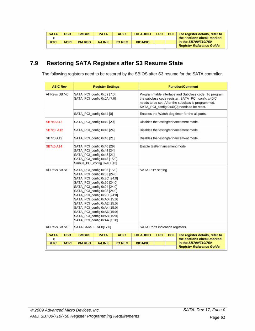
© 2009 Advanced Micro Devices, Inc. SATA: Dev-17, Func-0 AMD SB700/710/750 Register Programming Requirements Page 61
SATA USB SMBUS PATA AC97 HD AUDIO LPC PCI X
RTC ACPI PM REG A-LINK I/O REG XIOAPIC
For register details, refer to the sections check-marked in the SB700/710/750 Register Reference Guide.
7.9 Restoring SATA Registers after S3 Resume State
The following registers need to be restored by the SBIOS after S3 resume for the SATA controller.
ASIC Rev Register Settings Function/Comment
SATA_PCI_config 0x09 [7:0] SATA_PCI_config 0x0A [7:0]
Programmable interface and Subclass code. To program the subclass code register, SATA_PCI_config x40[0] needs to be set. After the subclass is programmed, SATA_PCI_config 0x40[0] needs to be reset.
All Revs SB7x0
SATA_PCI_config 0x44 [0] Enables the Watch-dog timer for the all ports.
SB7x0 A12 SATA_PCI_config 0x40 [29] Disables the testing/enhancement mode.
SB7x0 A12 SATA_PCI_config 0x48 [24] Disables the testing/enhancement mode.
SB7x0 A12 SATA_PCI_config 0x48 [21] Disables the testing/enhancement mode.
SB7x0 A14 SATA_PCI_config 0x40 [29] SATA_PCI_config 0x48 [24] SATA_PCI_config 0x48 [21] SATA_PCI_config 0x48 [15:9] Smbus_PCI_config 0xAC [13]
Enable test/enhancement mode
All Revs SB7x0 SATA_PCI_config 0x86 [15:0] SATA_PCI_config 0x88 [24:0] SATA_PCI_config 0x8C [24:0] SATA_PCI_config 0x90 [24:0] SATA_PCI_config 0x94 [24:0] SATA_PCI_config 0x98 [24:0] SATA_PCI_config 0x9C [24:0] SATA_PCI_config 0xA0 [15:0] SATA_PCI_config 0xA2 [15:0] SATA_PCI_config 0xA4 [15:0] SATA_PCI_config 0xA6 [15:0] SATA_PCI_config 0xA8 [15:0] SATA_PCI_config 0xAA [15:0]
SATA PHY setting.
All Revs SB7x0 SATA BAR5 + 0xF8[17:0] SATA Ports indication registers.
SATA USB SMBUS PATA AC97 HD AUDIO LPC PCI X
RTC ACPI PM REG A-LINK I/O REG XIOAPIC
For register details, refer to the sections check-marked in the SB700/710/750 Register Reference Guide.
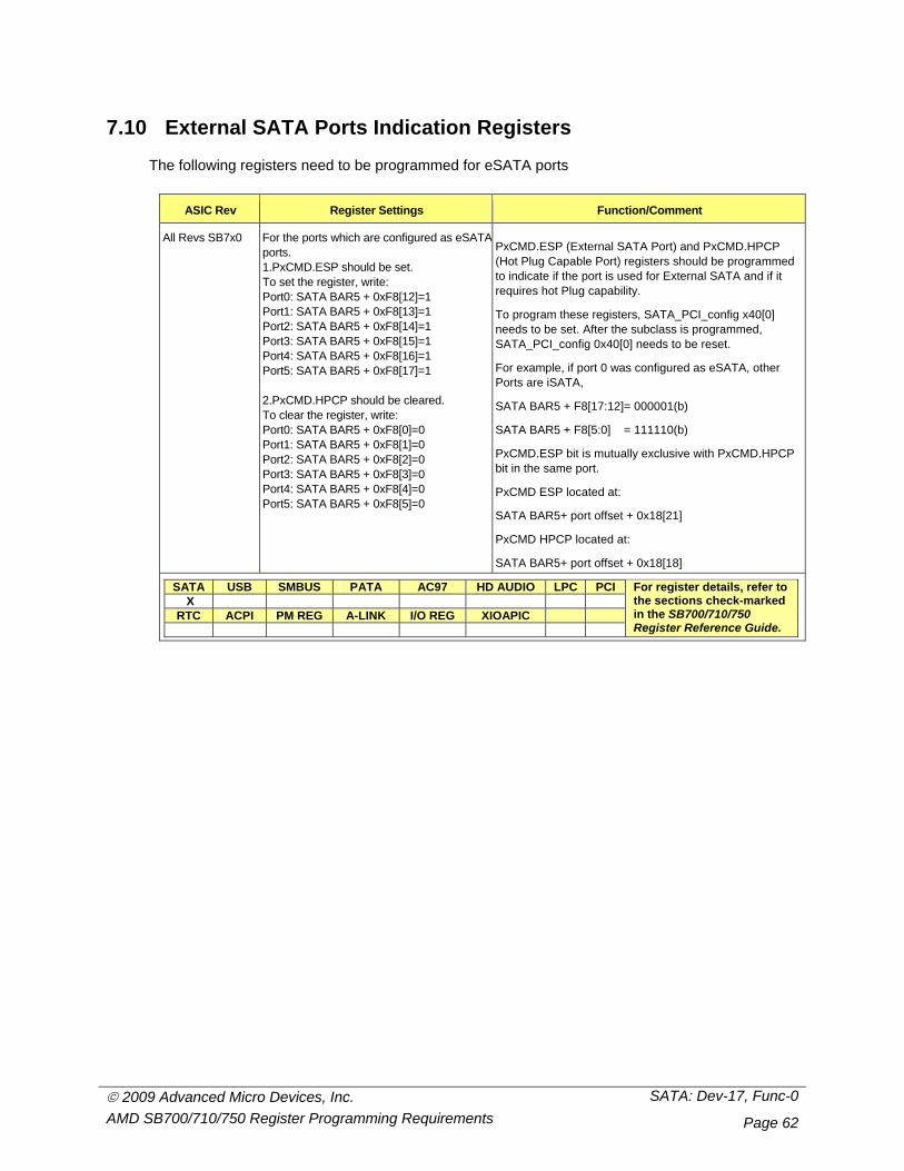
© 2009 Advanced Micro Devices, Inc. SATA: Dev-17, Func-0 AMD SB700/710/750 Register Programming Requirements Page 62
7.10 External SATA Ports Indication Registers
The following registers need to be programmed for eSATA ports
ASIC Rev Register Settings Function/Comment
All Revs SB7x0 For the ports which are configured as eSATAports. 1.PxCMD.ESP should be set. To set the register, write: Port0: SATA BAR5 + 0xF8[12]=1 Port1: SATA BAR5 + 0xF8[13]=1 Port2: SATA BAR5 + 0xF8[14]=1 Port3: SATA BAR5 + 0xF8[15]=1 Port4: SATA BAR5 + 0xF8[16]=1 Port5: SATA BAR5 + 0xF8[17]=1 2.PxCMD.HPCP should be cleared. To clear the register, write: Port0: SATA BAR5 + 0xF8[0]=0 Port1: SATA BAR5 + 0xF8[1]=0 Port2: SATA BAR5 + 0xF8[2]=0 Port3: SATA BAR5 + 0xF8[3]=0 Port4: SATA BAR5 + 0xF8[4]=0 Port5: SATA BAR5 + 0xF8[5]=0
PxCMD.ESP (External SATA Port) and PxCMD.HPCP (Hot Plug Capable Port) registers should be programmed to indicate if the port is used for External SATA and if it requires hot Plug capability.
To program these registers, SATA_PCI_config x40[0] needs to be set. After the subclass is programmed, SATA_PCI_config 0x40[0] needs to be reset.
For example, if port 0 was configured as eSATA, other Ports are iSATA,
SATA BAR5 + F8[17:12]= 000001(b)
SATA BAR5 + F8[5:0] = 111110(b)
PxCMD.ESP bit is mutually exclusive with PxCMD.HPCP bit in the same port.
PxCMD ESP located at:
SATA BAR5+ port offset + 0x18[21]
PxCMD HPCP located at:
SATA BAR5+ port offset + 0x18[18]
SATA USB SMBUS PATA AC97 HD AUDIO LPC PCI X
RTC ACPI PM REG A-LINK I/O REG XIOAPIC
For register details, refer to the sections check-marked in the SB700/710/750 Register Reference Guide.
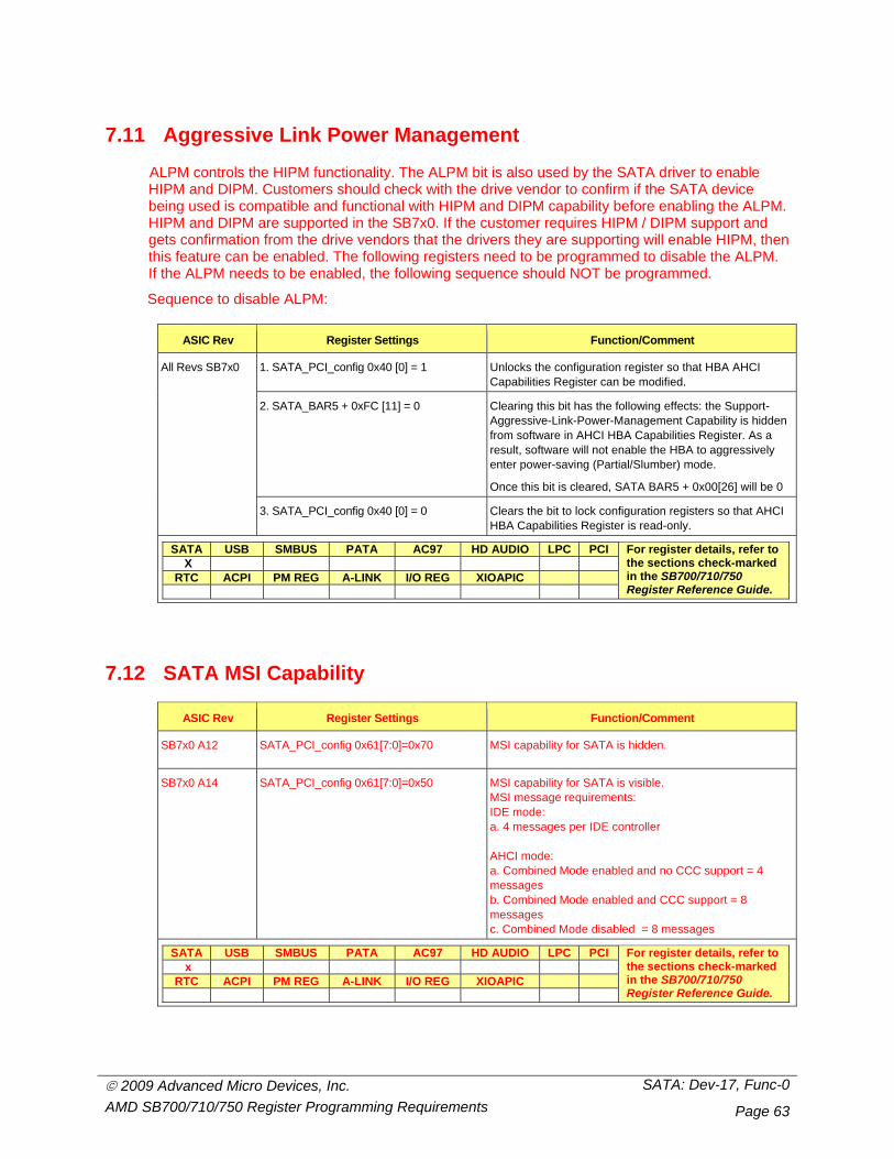
© 2009 Advanced Micro Devices, Inc. SATA: Dev-17, Func-0 AMD SB700/710/750 Register Programming Requirements Page 63
7.11 Aggressive Link Power Management
ALPM controls the HIPM functionality. The ALPM bit is also used by the SATA driver to enable HIPM and DIPM. Customers should check with the drive vendor to confirm if the SATA device being used is compatible and functional with HIPM and DIPM capability before enabling the ALPM. HIPM and DIPM are supported in the SB7x0. If the customer requires HIPM / DIPM support and gets confirmation from the drive vendors that the drivers they are supporting will enable HIPM, then this feature can be enabled. The following registers need to be programmed to disable the ALPM. If the ALPM needs to be enabled, the following sequence should NOT be programmed.
Sequence to disable ALPM:
ASIC Rev Register Settings Function/Comment
1. SATA_PCI_config 0x40 [0] = 1 Unlocks the configuration register so that HBA AHCI Capabilities Register can be modified.
2. SATA_BAR5 + 0xFC [11] = 0
Clearing this bit has the following effects: the Support-Aggressive-Link-Power-Management Capability is hidden from software in AHCI HBA Capabilities Register. As a result, software will not enable the HBA to aggressively enter power-saving (Partial/Slumber) mode.
Once this bit is cleared, SATA BAR5 + 0x00[26] will be 0
All Revs SB7x0
3. SATA_PCI_config 0x40 [0] = 0 Clears the bit to lock configuration registers so that AHCI HBA Capabilities Register is read-only.
SATA USB SMBUS PATA AC97 HD AUDIO LPC PCI X
RTC ACPI PM REG A-LINK I/O REG XIOAPIC
For register details, refer to the sections check-marked in the SB700/710/750 Register Reference Guide.
7.12 SATA MSI Capability
ASIC Rev Register Settings Function/Comment
SB7x0 A12 SATA_PCI_config 0x61[7:0]=0x70
MSI capability for SATA is hidden.
SB7x0 A14 SATA_PCI_config 0x61[7:0]=0x50
MSI capability for SATA is visible. MSI message requirements: IDE mode: a. 4 messages per IDE controller AHCI mode: a. Combined Mode enabled and no CCC support = 4 messages b. Combined Mode enabled and CCC support = 8 messages c. Combined Mode disabled = 8 messages
SATA USB SMBUS PATA AC97 HD AUDIO LPC PCI x
RTC ACPI PM REG A-LINK I/O REG XIOAPIC
For register details, refer to the sections check-marked in the SB700/710/750 Register Reference Guide.
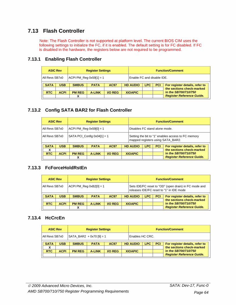
© 2009 Advanced Micro Devices, Inc. SATA: Dev-17, Func-0 AMD SB700/710/750 Register Programming Requirements Page 64
7.13 Flash Controller
Note: The Flash Controller is not supported at platform level. The current BIOS CIM uses the following settings to initialize the FC, if it is enabled. The default setting is for FC disabled. If FC is disabled in the hardware, the registers below are not required to be programmed.
7.13.1 Enabling Flash Controller
ASIC Rev Register Settings Function/Comment
All Revs SB7x0 ACPI PM_Reg 0x59[1] = 1 Enable FC and disable IDE.
SATA USB SMBUS PATA AC97 HD AUDIO LPC PCI
RTC ACPI PM REG A-LINK I/O REG XIOAPIC X
For register details, refer to the sections check-marked in the SB700/710/750 Register Reference Guide.
7.13.2 Config SATA BAR2 for Flash Controller
ASIC Rev Register Settings Function/Comment
All Revs SB7x0 ACPI PM_Reg 0x59[0] = 1 Disables FC stand alone mode.
All Revs SB7x0 SATA PCI_Config 0x04[1] = 1 Setting the bit to “1” enables access to FC memory mapped registers using SATA_BAR2.
SATA USB SMBUS PATA AC97 HD AUDIO LPC PCI X
RTC ACPI PM REG A-LINK I/O REG XIOAPIC X
For register details, refer to the sections check-marked in the SB700/710/750 Register Reference Guide.
7.13.3 FcForceHoldRstEn
ASIC Rev Register Settings Function/Comment
All Revs SB7x0 ACPI PM_Reg 0xB2[0] = 1 Sets IDE/FC reset to “OD” (open drain) in FC mode and releases IDE/FC reset to “1” in IDE mode
SATA USB SMBUS PATA AC97 HD AUDIO LPC PCI
RTC ACPI PM REG A-LINK I/O REG XIOAPIC X
For register details, refer to the sections check-marked in the SB700/710/750 Register Reference Guide.
7.13.4 HcCrcEn
ASIC Rev Register Settings Function/Comment
All Revs SB7x0 SATA_BAR2 + 0x70 [9] = 1 Enables HC CRC.
SATA USB SMBUS PATA AC97 HD AUDIO LPC PCI X
RTC ACPI PM REG A-LINK I/O REG XIOAPIC
For register details, refer to the sections check-marked in the SB700/710/750 Register Reference Guide.
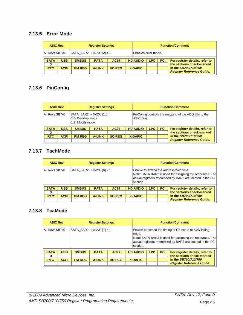
© 2009 Advanced Micro Devices, Inc. SATA: Dev-17, Func-0 AMD SB700/710/750 Register Programming Requirements Page 65
7.13.5 Error Mode
ASIC Rev Register Settings Function/Comment
All Revs SB7x0 SATA_BAR2 + 0x70 [12] = 1 Enables error mode.
SATA USB SMBUS PATA AC97 HD AUDIO LPC PCI X
RTC ACPI PM REG A-LINK I/O REG XIOAPIC
For register details, refer to the sections check-marked in the SB700/710/750 Register Reference Guide.
7.13.6 PinConfig
ASIC Rev Register Settings Function/Comment
All Revs SB7x0 SATA_BAR2 + 0x200 [1:0] 0x0: Desktop mode 0x2: Mobile mode
PinConfig controls the mapping of the ADQ bits to the ASIC pins.
SATA USB SMBUS PATA AC97 HD AUDIO LPC PCI X
RTC ACPI PM REG A-LINK I/O REG XIOAPIC
For register details, refer to the sections check-marked in the SB700/710/750 Register Reference Guide.
7.13.7 TachMode
ASIC Rev Register Settings Function/Comment
All Revs SB7x0 SATA_BAR2 + 0x200 [6] = 1 Enable to extend the address hold time. Note: SATA BAR2 is used for assigning the resources. Theactual registers referenced by BAR2 are located in the FC section.
SATA USB SMBUS PATA AC97 HD AUDIO LPC PCI X
RTC ACPI PM REG A-LINK I/O REG XIOAPIC
For register details, refer to the sections check-marked in the SB700/710/750 Register Reference Guide.
7.13.8 TcaMode
ASIC Rev Register Settings Function/Comment
All Revs SB7x0 SATA_BAR2 + 0x200 [7] = 1 Enable to extend the timing of CE setup to AVD falling edge. Note: SATA BAR2 is used for assigning the resources. Theactual registers referenced by BAR2 are located in the FC section.
SATA USB SMBUS PATA AC97 HD AUDIO LPC PCI X
RTC ACPI PM REG A-LINK I/O REG XIOAPIC
For register details, refer to the sections check-marked in the SB700/710/750 Register Reference Guide.
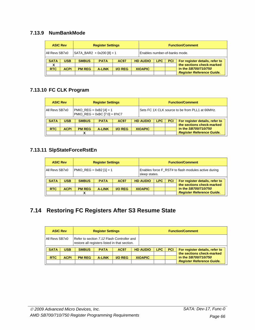
© 2009 Advanced Micro Devices, Inc. SATA: Dev-17, Func-0 AMD SB700/710/750 Register Programming Requirements Page 66
7.13.9 NumBankMode
ASIC Rev Register Settings Function/Comment
All Revs SB7x0 SATA_BAR2 + 0x200 [8] = 1 Enables number-of-banks mode.
SATA USB SMBUS PATA AC97 HD AUDIO LPC PCI X
RTC ACPI PM REG A-LINK I/O REG XIOAPIC
For register details, refer to the sections check-marked in the SB700/710/750 Register Reference Guide.
7.13.10 FC CLK Program
ASIC Rev Register Settings Function/Comment
All Revs SB7x0 PMIO_REG + 0xB2 [4] = 1 PMIO_REG + 0xBC [7:0] = 8’hC7
Sets FC 1X CLK source to be from PLL1 at 66MHz.
SATA USB SMBUS PATA AC97 HD AUDIO LPC PCI
RTC ACPI PM REG A-LINK I/O REG XIOAPIC X
For register details, refer to the sections check-marked in the SB700/710/750 Register Reference Guide.
7.13.11 SlpStateForceRstEn
ASIC Rev Register Settings Function/Comment
All Revs SB7x0 PMIO_REG + 0xB2 [1] = 1
Enables force F_RST# to flash modules active during sleep states.
SATA USB SMBUS PATA AC97 HD AUDIO LPC PCI
RTC ACPI PM REG A-LINK I/O REG XIOAPIC X
For register details, refer to the sections check-marked in the SB700/710/750 Register Reference Guide.
7.14 Restoring FC Registers After S3 Resume State
ASIC Rev Register Settings Function/Comment
All Revs SB7x0 Refer to section 7.12 Flash Controller and restore all registers listed in that section.
SATA USB SMBUS PATA AC97 HD AUDIO LPC PCI
RTC ACPI PM REG A-LINK I/O REG XIOAPIC
For register details, refer to the sections check-marked in the SB700/710/750 Register Reference Guide.
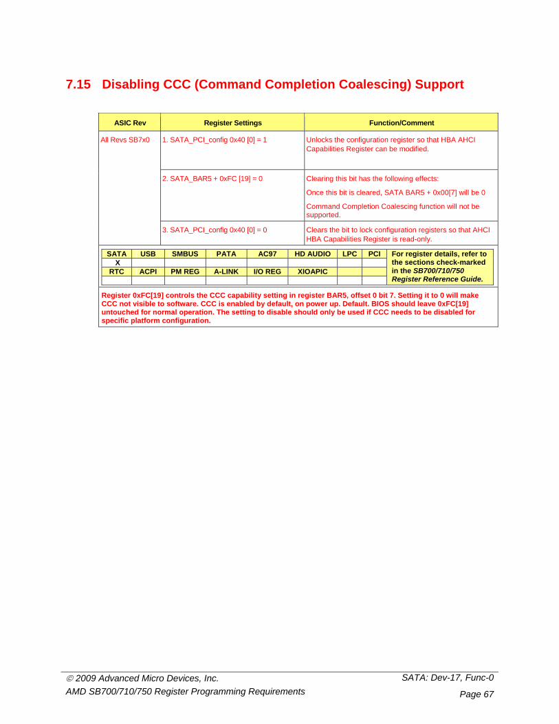
© 2009 Advanced Micro Devices, Inc. SATA: Dev-17, Func-0 AMD SB700/710/750 Register Programming Requirements Page 67
7.15 Disabling CCC (Command Completion Coalescing) Support
ASIC Rev Register Settings Function/Comment
1. SATA_PCI_config 0x40 [0] = 1 Unlocks the configuration register so that HBA AHCI Capabilities Register can be modified.
2. SATA_BAR5 + 0xFC [19] = 0
Clearing this bit has the following effects:
Once this bit is cleared, SATA BAR5 + 0x00[7] will be 0
Command Completion Coalescing function will not be supported.
All Revs SB7x0
3. SATA_PCI_config 0x40 [0] = 0 Clears the bit to lock configuration registers so that AHCI HBA Capabilities Register is read-only.
SATA USB SMBUS PATA AC97 HD AUDIO LPC PCI X
RTC ACPI PM REG A-LINK I/O REG XIOAPIC
For register details, refer to the sections check-marked in the SB700/710/750 Register Reference Guide.
Register 0xFC[19] controls the CCC capability setting in register BAR5, offset 0 bit 7. Setting it to 0 will make CCC not visible to software. CCC is enabled by default, on power up. Default. BIOS should leave 0xFC[19] untouched for normal operation. The setting to disable should only be used if CCC needs to be disabled for specific platform configuration.
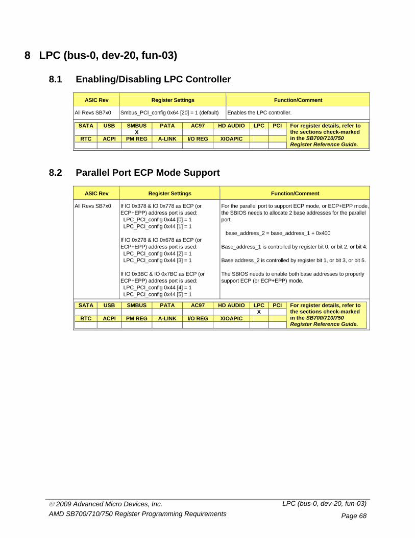
© 2009 Advanced Micro Devices, Inc. LPC (bus-0, dev-20, fun-03) AMD SB700/710/750 Register Programming Requirements Page 68
8 LPC (bus-0, dev-20, fun-03)
8.1 Enabling/Disabling LPC Controller
ASIC Rev Register Settings Function/Comment
All Revs SB7x0 Smbus_PCI_config 0x64 [20] = 1 (default) Enables the LPC controller.
SATA USB SMBUS PATA AC97 HD AUDIO LPC PCI X
RTC ACPI PM REG A-LINK I/O REG XIOAPIC
For register details, refer to the sections check-marked in the SB700/710/750 Register Reference Guide.
8.2 Parallel Port ECP Mode Support
ASIC Rev Register Settings Function/Comment
All Revs SB7x0 If IO 0x378 & IO 0x778 as ECP (or ECP+EPP) address port is used: LPC_PCI_config 0x44 [0] = 1 LPC_PCI_config 0x44 [1] = 1 If IO 0x278 & IO 0x678 as ECP (or ECP+EPP) address port is used: LPC_PCI_config 0x44 [2] = 1 LPC_PCI_config 0x44 [3] = 1 If IO 0x3BC & IO 0x7BC as ECP (or ECP+EPP) address port is used: LPC_PCI_config 0x44 [4] = 1 LPC_PCI_config 0x44 [5] = 1
For the parallel port to support ECP mode, or ECP+EPP mode, the SBIOS needs to allocate 2 base addresses for the parallel port. base_address_2 = base_address_1 + 0x400 Base_address_1 is controlled by register bit 0, or bit 2, or bit 4. Base address_2 is controlled by register bit 1, or bit 3, or bit 5. The SBIOS needs to enable both base addresses to properly support ECP (or ECP+EPP) mode.
SATA USB SMBUS PATA AC97 HD AUDIO LPC PCI X
RTC ACPI PM REG A-LINK I/O REG XIOAPIC
For register details, refer to the sections check-marked in the SB700/710/750 Register Reference Guide.
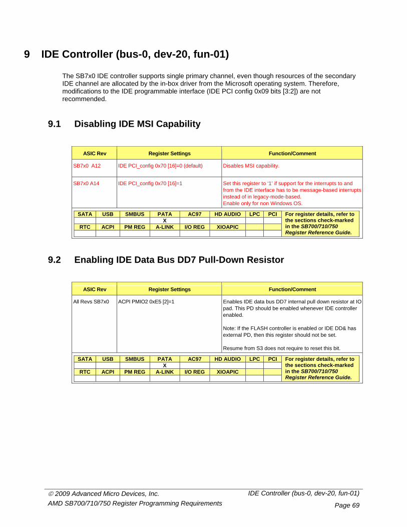
© 2009 Advanced Micro Devices, Inc. IDE Controller (bus-0, dev-20, fun-01) AMD SB700/710/750 Register Programming Requirements Page 69
9 IDE Controller (bus-0, dev-20, fun-01)
The SB7x0 IDE controller supports single primary channel, even though resources of the secondary IDE channel are allocated by the in-box driver from the Microsoft operating system. Therefore, modifications to the IDE programmable interface (IDE PCI config 0x09 bits [3:2]) are not recommended.
9.1 Disabling IDE MSI Capability
ASIC Rev Register Settings Function/Comment
SB7x0 A12 IDE PCI_config 0x70 [16]=0 (default)
Disables MSI capability.
SB7x0 A14
IDE PCI_config 0x70 [16]=1
Set this register to ‘1’ if support for the interrupts to and from the IDE interface has to be message-based interrupts instead of in legacy-mode-based. Enable only for non Windows OS.
SATA USB SMBUS PATA AC97 HD AUDIO LPC PCI X
RTC ACPI PM REG A-LINK I/O REG XIOAPIC
For register details, refer to the sections check-marked in the SB700/710/750 Register Reference Guide.
9.2 Enabling IDE Data Bus DD7 Pull-Down Resistor
ASIC Rev Register Settings Function/Comment
All Revs SB7x0 ACPI PMIO2 0xE5 [2]=1
Enables IDE data bus DD7 internal pull down resistor at IO pad. This PD should be enabled whenever IDE controller enabled. Note: If the FLASH controller is enabled or IDE DD& has external PD, then this register should not be set. Resume from S3 does not require to reset this bit.
SATA USB SMBUS PATA AC97 HD AUDIO LPC PCI X
RTC ACPI PM REG A-LINK I/O REG XIOAPIC
For register details, refer to the sections check-marked in the SB700/710/750 Register Reference Guide.
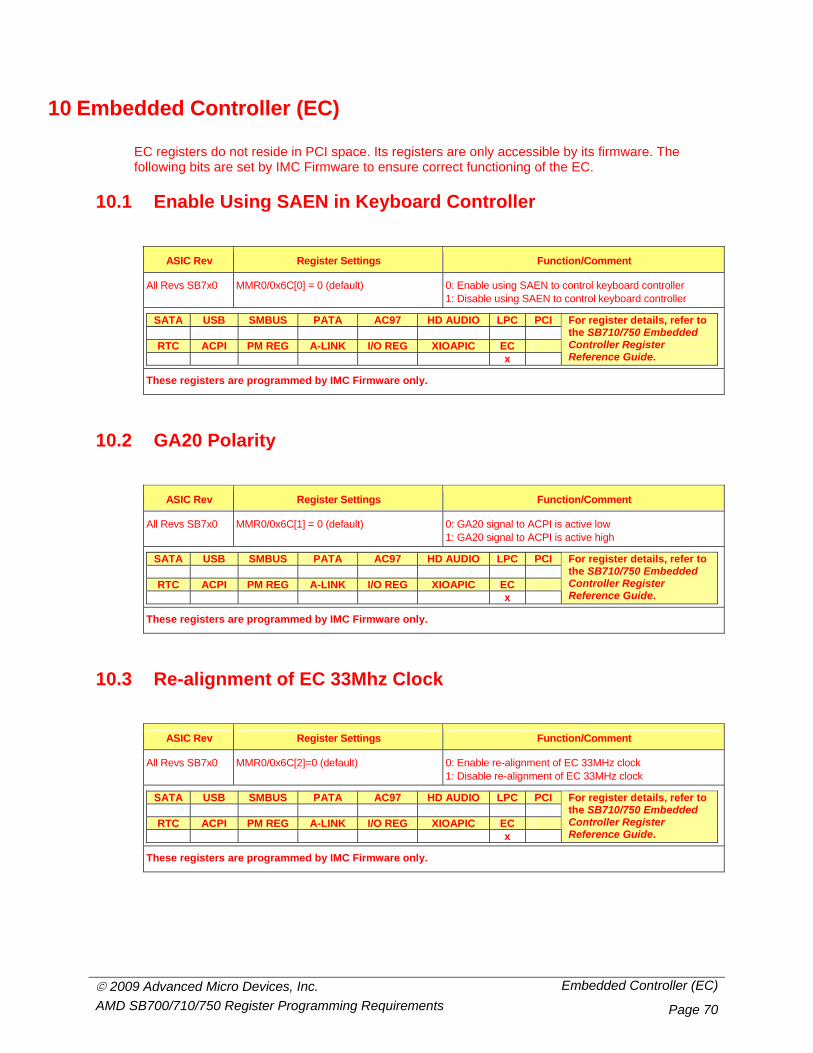
© 2009 Advanced Micro Devices, Inc. Embedded Controller (EC)AMD SB700/710/750 Register Programming Requirements Page 70
10 Embedded Controller (EC)
EC registers do not reside in PCI space. Its registers are only accessible by its firmware. The following bits are set by IMC Firmware to ensure correct functioning of the EC.
10.1 Enable Using SAEN in Keyboard Controller
ASIC Rev Register Settings Function/Comment
All Revs SB7x0 MMR0/0x6C[0] = 0 (default) 0: Enable using SAEN to control keyboard controller 1: Disable using SAEN to control keyboard controller
SATA USB SMBUS PATA AC97 HD AUDIO LPC PCI
RTC ACPI PM REG A-LINK I/O REG XIOAPIC EC x
For register details, refer to the SB710/750 Embedded Controller Register Reference Guide.
These registers are programmed by IMC Firmware only.
10.2 GA20 Polarity
ASIC Rev Register Settings Function/Comment
All Revs SB7x0 MMR0/0x6C[1] = 0 (default) 0: GA20 signal to ACPI is active low 1: GA20 signal to ACPI is active high
SATA USB SMBUS PATA AC97 HD AUDIO LPC PCI
RTC ACPI PM REG A-LINK I/O REG XIOAPIC EC x
For register details, refer to the SB710/750 Embedded Controller Register Reference Guide.
These registers are programmed by IMC Firmware only.
10.3 Re-alignment of EC 33Mhz Clock
ASIC Rev Register Settings Function/Comment
All Revs SB7x0 MMR0/0x6C[2]=0 (default) 0: Enable re-alignment of EC 33MHz clock 1: Disable re-alignment of EC 33MHz clock
SATA USB SMBUS PATA AC97 HD AUDIO LPC PCI
RTC ACPI PM REG A-LINK I/O REG XIOAPIC EC x
For register details, refer to the SB710/750 Embedded Controller Register Reference Guide.
These registers are programmed by IMC Firmware only.
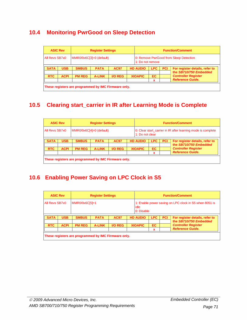
© 2009 Advanced Micro Devices, Inc. Embedded Controller (EC)AMD SB700/710/750 Register Programming Requirements Page 71
10.4 Monitoring PwrGood on Sleep Detection
ASIC Rev Register Settings Function/Comment
All Revs SB7x0 MMR0/0x6C[3]=0 (default) 0: Remove PwrGood from Sleep Detection 1: Do not remove
SATA USB SMBUS PATA AC97 HD AUDIO LPC PCI
RTC ACPI PM REG A-LINK I/O REG XIOAPIC EC x
For register details, refer to the SB710/750 Embedded Controller Register Reference Guide.
These registers are programmed by IMC Firmware only.
10.5 Clearing start_carrier in IR after Learning Mode is Complete
ASIC Rev Register Settings Function/Comment
All Revs SB7x0 MMR0/0x6C[4]=0 (default) 0: Clear start_carrier in IR after learning mode is complete 1: Do not clear
SATA USB SMBUS PATA AC97 HD AUDIO LPC PCI
RTC ACPI PM REG A-LINK I/O REG XIOAPIC EC x
For register details, refer to the SB710/750 Embedded Controller Register Reference Guide.
These registers are programmed by IMC Firmware only.
10.6 Enabling Power Saving on LPC Clock in S5
ASIC Rev Register Settings Function/Comment
All Revs SB7x0 MMR0/0x6C[5]=1 1: Enable power saving on LPC clock in S5 when 8051 is idle 0: Disable
SATA USB SMBUS PATA AC97 HD AUDIO LPC PCI
RTC ACPI PM REG A-LINK I/O REG XIOAPIC EC x
For register details, refer to the SB710/750 Embedded Controller Register Reference Guide.
These registers are programmed by IMC Firmware only.
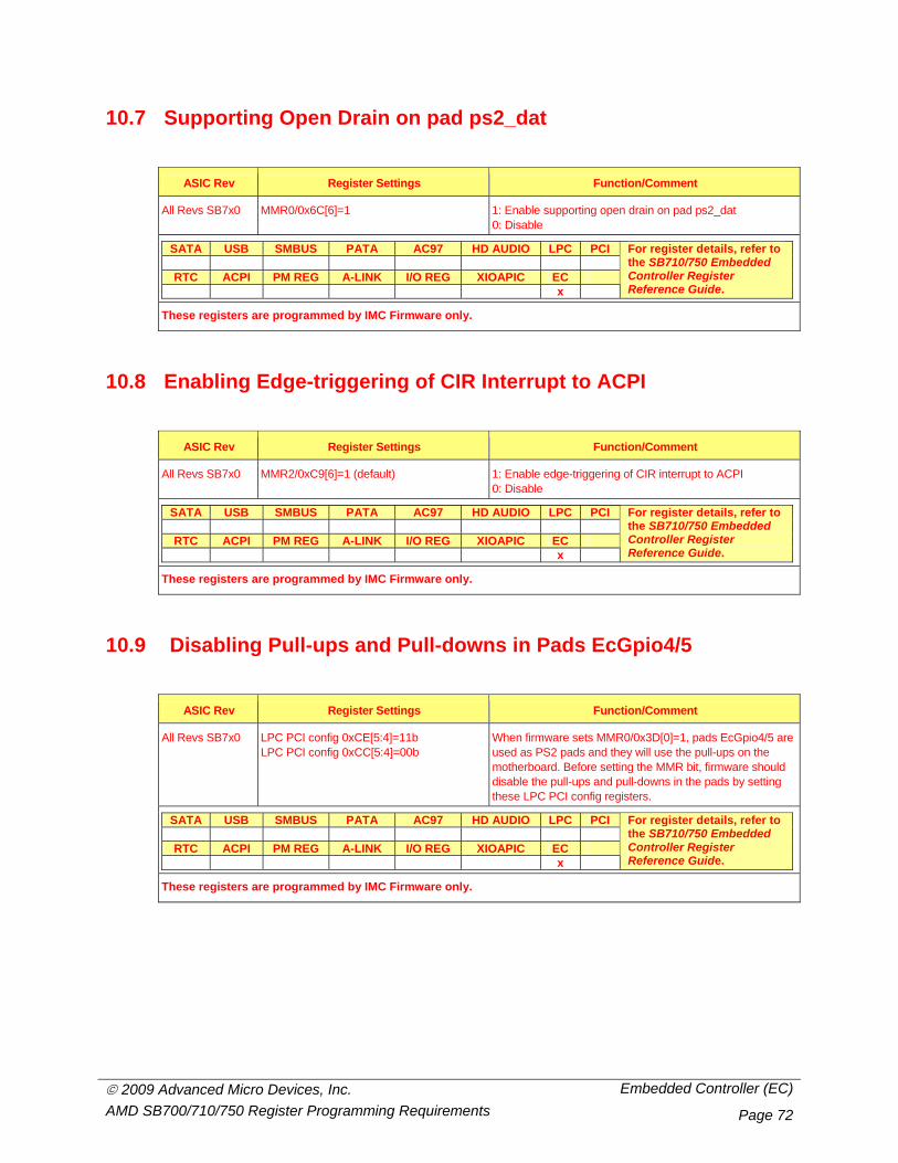
© 2009 Advanced Micro Devices, Inc. Embedded Controller (EC)AMD SB700/710/750 Register Programming Requirements Page 72
10.7 Supporting Open Drain on pad ps2_dat
ASIC Rev Register Settings Function/Comment
All Revs SB7x0 MMR0/0x6C[6]=1 1: Enable supporting open drain on pad ps2_dat 0: Disable
SATA USB SMBUS PATA AC97 HD AUDIO LPC PCI
RTC ACPI PM REG A-LINK I/O REG XIOAPIC EC x
For register details, refer to the SB710/750 Embedded Controller Register Reference Guide.
These registers are programmed by IMC Firmware only.
10.8 Enabling Edge-triggering of CIR Interrupt to ACPI
ASIC Rev Register Settings Function/Comment
All Revs SB7x0 MMR2/0xC9[6]=1 (default) 1: Enable edge-triggering of CIR interrupt to ACPI 0: Disable
SATA USB SMBUS PATA AC97 HD AUDIO LPC PCI
RTC ACPI PM REG A-LINK I/O REG XIOAPIC EC x
For register details, refer to the SB710/750 Embedded Controller Register Reference Guide.
These registers are programmed by IMC Firmware only.
10.9 Disabling Pull-ups and Pull-downs in Pads EcGpio4/5
ASIC Rev Register Settings Function/Comment
All Revs SB7x0 LPC PCI config 0xCE[5:4]=11b LPC PCI config 0xCC[5:4]=00b
When firmware sets MMR0/0x3D[0]=1, pads EcGpio4/5 are used as PS2 pads and they will use the pull-ups on the motherboard. Before setting the MMR bit, firmware should disable the pull-ups and pull-downs in the pads by setting these LPC PCI config registers.
SATA USB SMBUS PATA AC97 HD AUDIO LPC PCI
RTC ACPI PM REG A-LINK I/O REG XIOAPIC EC x
For register details, refer to the SB710/750 Embedded Controller Register Reference Guide.
These registers are programmed by IMC Firmware only.
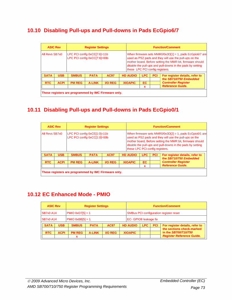
© 2009 Advanced Micro Devices, Inc. Embedded Controller (EC)AMD SB700/710/750 Register Programming Requirements Page 73
10.10 Disabling Pull-ups and Pull-downs in Pads EcGpio6/7
ASIC Rev Register Settings Function/Comment
All Revs SB7x0 LPC PCI config 0xCE[7:6]=11b LPC PCI config 0xCC[7:6]=00b
When firmware sets MMR0/0x3D[1] = 1, pads EcGpio6/7 areused as PS2 pads and they will use the pull-ups on the mother board. Before setting the MMR bit, firmware should disable the pull-ups and pull-downs in the pads by setting these LPC PCI config registers.
SATA USB SMBUS PATA AC97 HD AUDIO LPC PCI
RTC ACPI PM REG A-LINK I/O REG XIOAPIC EC x
For register details, refer to the SB710/750 Embedded Controller Register Reference Guide.
These registers are programmed by IMC Firmware only.
10.11 Disabling Pull-ups and Pull-downs in Pads EcGpio0/1
ASIC Rev Register Settings Function/Comment
All Revs SB7x0 LPC PCI config 0xCE[1:0]=11b LPC PCI config 0xCC[1:0]=00b
When firmware sets MMR0/0x3D[2] = 1, pads EcGpio0/1 areused as PS2 pads and they will use the pull-ups on the mother board. Before setting the MMR bit, firmware should disable the pull-ups and pull-downs in the pads by setting these LPC PCI config registers.
SATA USB SMBUS PATA AC97 HD AUDIO LPC PCI
RTC ACPI PM REG A-LINK I/O REG XIOAPIC EC x
For register details, refer to the SB710/750 Embedded Controller Register Reference Guide.
These registers are programmed by IMC Firmware only.
10.12 EC Enhanced Mode - PMIO
ASIC Rev Register Settings Function/Comment
SB7x0 A14 PMIO 0xD7[5] = 1 SMBus PCI configuration register reset
SB7x0 A14 PMIO 0xBB[5] = 1 EC- GPIO8 leakage fix
SATA USB SMBUS PATA AC97 HD AUDIO LPC PCI
RTC ACPI PM REG A-LINK I/O REG XIOAPIC x
For register details, refer to the sections check-marked in the SB700/710/750 Register Reference Guide.
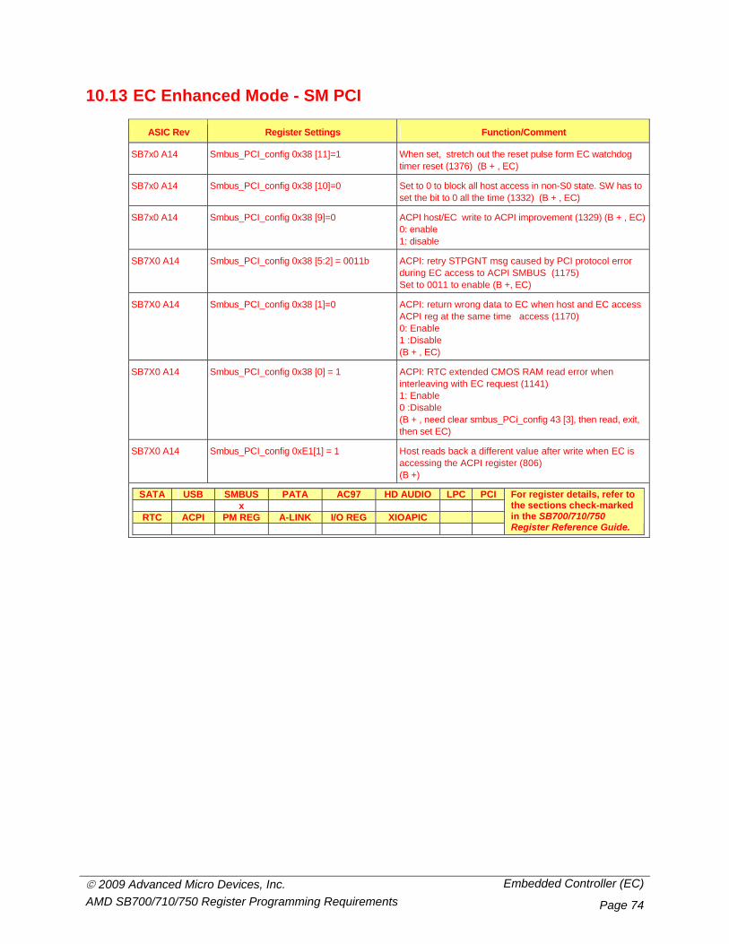
© 2009 Advanced Micro Devices, Inc. Embedded Controller (EC)AMD SB700/710/750 Register Programming Requirements Page 74
10.13 EC Enhanced Mode - SM PCI
ASIC Rev Register Settings Function/Comment
SB7x0 A14
Smbus_PCI_config 0x38 [11]=1
When set, stretch out the reset pulse form EC watchdog timer reset (1376) (B + , EC)
SB7x0 A14
Smbus_PCI_config 0x38 [10]=0
Set to 0 to block all host access in non-S0 state. SW has to set the bit to 0 all the time (1332) (B + , EC)
SB7x0 A14
Smbus_PCI_config 0x38 [9]=0
ACPI host/EC write to ACPI improvement (1329) (B + , EC)0: enable 1: disable
SB7X0 A14
Smbus_PCI_config 0x38 [5:2] = 0011b
ACPI: retry STPGNT msg caused by PCI protocol error during EC access to ACPI SMBUS (1175) Set to 0011 to enable (B +, EC)
SB7X0 A14
Smbus_PCI_config 0x38 [1]=0
ACPI: return wrong data to EC when host and EC access ACPI reg at the same time access (1170) 0: Enable 1 :Disable (B + , EC)
SB7X0 A14
Smbus_PCI_config 0x38 [0] = 1
ACPI: RTC extended CMOS RAM read error when interleaving with EC request (1141) 1: Enable 0 :Disable (B + , need clear smbus_PCi_config 43 [3], then read, exit, then set EC)
SB7X0 A14
Smbus_PCI_config 0xE1[1] = 1
Host reads back a different value after write when EC is accessing the ACPI register (806) (B +)
SATA USB SMBUS PATA AC97 HD AUDIO LPC PCI x
RTC ACPI PM REG A-LINK I/O REG XIOAPIC
For register details, refer to the sections check-marked in the SB700/710/750 Register Reference Guide.
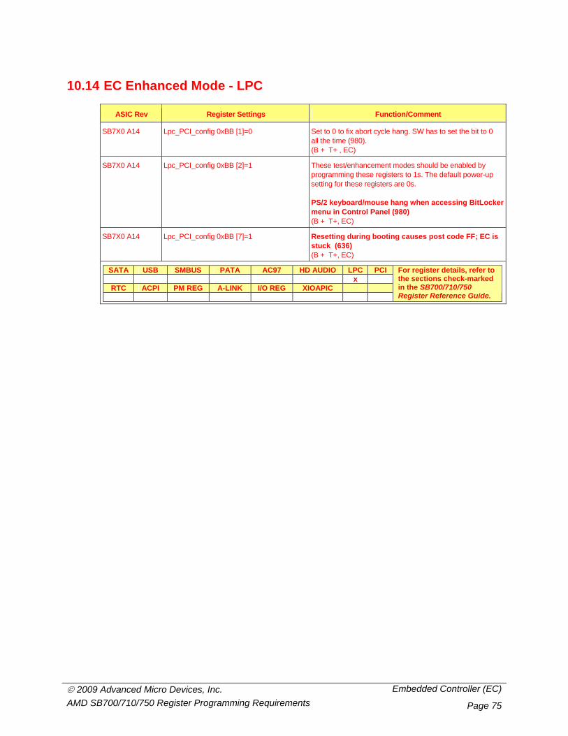
© 2009 Advanced Micro Devices, Inc. Embedded Controller (EC)AMD SB700/710/750 Register Programming Requirements Page 75
10.14 EC Enhanced Mode - LPC
ASIC Rev Register Settings Function/Comment
SB7X0 A14
Lpc_PCI_config 0xBB [1]=0
Set to 0 to fix abort cycle hang. SW has to set the bit to 0 all the time (980). (B + T+ , EC)
SB7X0 A14
Lpc_PCI_config 0xBB [2]=1
These test/enhancement modes should be enabled by programming these registers to 1s. The default power-up setting for these registers are 0s. PS/2 keyboard/mouse hang when accessing BitLocker menu in Control Panel (980) (B + T+, EC)
SB7X0 A14
Lpc_PCI_config 0xBB [7]=1
Resetting during booting causes post code FF; EC is stuck (636) (B + T+, EC)
SATA USB SMBUS PATA AC97 HD AUDIO LPC PCI x
RTC ACPI PM REG A-LINK I/O REG XIOAPIC
For register details, refer to the sections check-marked in the SB700/710/750 Register Reference Guide.
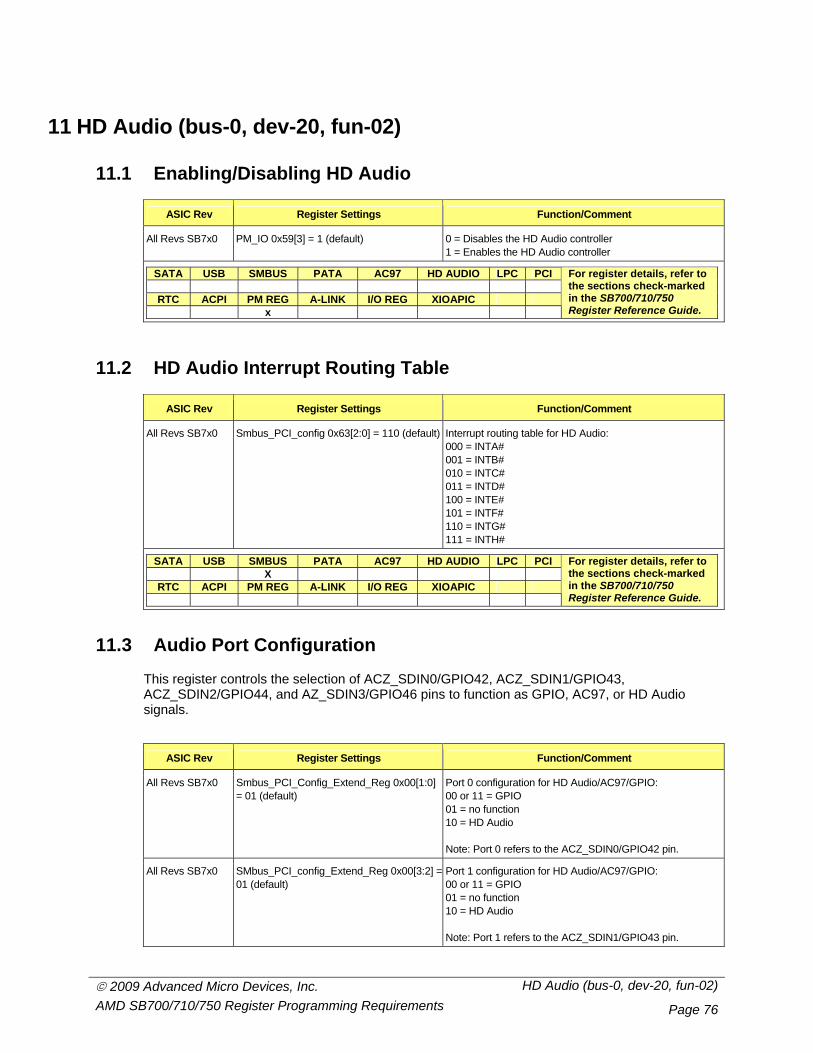
© 2009 Advanced Micro Devices, Inc. HD Audio (bus-0, dev-20, fun-02) AMD SB700/710/750 Register Programming Requirements Page 76
11 HD Audio (bus-0, dev-20, fun-02)
11.1 Enabling/Disabling HD Audio
ASIC Rev Register Settings Function/Comment
All Revs SB7x0 PM_IO 0x59[3] = 1 (default) 0 = Disables the HD Audio controller 1 = Enables the HD Audio controller
SATA USB SMBUS PATA AC97 HD AUDIO LPC PCI
RTC ACPI PM REG A-LINK I/O REG XIOAPIC x
For register details, refer to the sections check-marked in the SB700/710/750 Register Reference Guide.
11.2 HD Audio Interrupt Routing Table
ASIC Rev Register Settings Function/Comment
All Revs SB7x0 Smbus_PCI_config 0x63[2:0] = 110 (default) Interrupt routing table for HD Audio: 000 = INTA# 001 = INTB# 010 = INTC# 011 = INTD# 100 = INTE# 101 = INTF# 110 = INTG# 111 = INTH#
SATA USB SMBUS PATA AC97 HD AUDIO LPC PCI X
RTC ACPI PM REG A-LINK I/O REG XIOAPIC
For register details, refer to the sections check-marked in the SB700/710/750 Register Reference Guide.
11.3 Audio Port Configuration
This register controls the selection of ACZ_SDIN0/GPIO42, ACZ_SDIN1/GPIO43, ACZ_SDIN2/GPIO44, and AZ_SDIN3/GPIO46 pins to function as GPIO, AC97, or HD Audio signals.
ASIC Rev Register Settings Function/Comment
All Revs SB7x0 Smbus_PCI_Config_Extend_Reg 0x00[1:0] = 01 (default)
Port 0 configuration for HD Audio/AC97/GPIO: 00 or 11 = GPIO 01 = no function 10 = HD Audio Note: Port 0 refers to the ACZ_SDIN0/GPIO42 pin.
All Revs SB7x0 SMbus_PCI_config_Extend_Reg 0x00[3:2] = 01 (default)
Port 1 configuration for HD Audio/AC97/GPIO: 00 or 11 = GPIO 01 = no function 10 = HD Audio Note: Port 1 refers to the ACZ_SDIN1/GPIO43 pin.
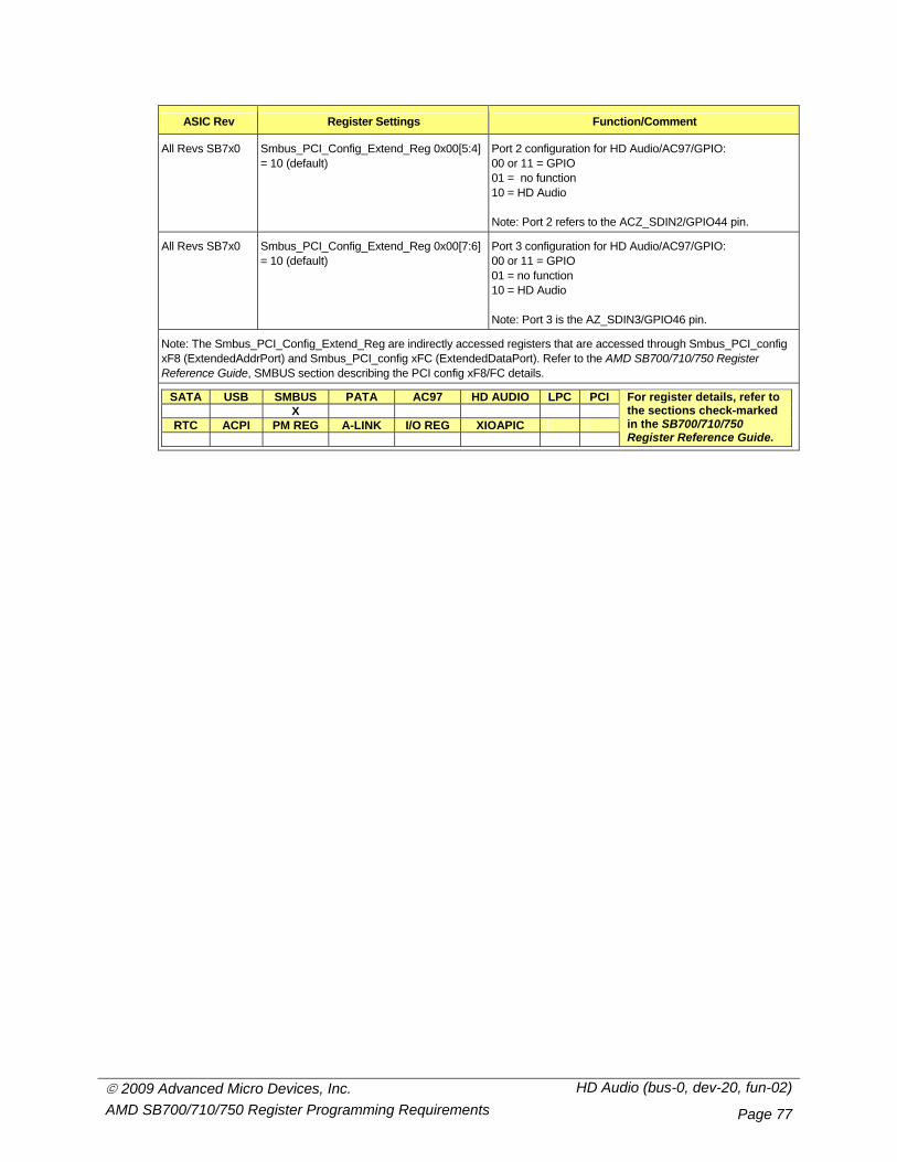
© 2009 Advanced Micro Devices, Inc. HD Audio (bus-0, dev-20, fun-02) AMD SB700/710/750 Register Programming Requirements Page 77
ASIC Rev Register Settings Function/Comment
All Revs SB7x0 Smbus_PCI_Config_Extend_Reg 0x00[5:4] = 10 (default)
Port 2 configuration for HD Audio/AC97/GPIO: 00 or 11 = GPIO 01 = no function 10 = HD Audio Note: Port 2 refers to the ACZ_SDIN2/GPIO44 pin.
All Revs SB7x0 Smbus_PCI_Config_Extend_Reg 0x00[7:6] = 10 (default)
Port 3 configuration for HD Audio/AC97/GPIO: 00 or 11 = GPIO 01 = no function 10 = HD Audio Note: Port 3 is the AZ_SDIN3/GPIO46 pin.
Note: The Smbus_PCI_Config_Extend_Reg are indirectly accessed registers that are accessed through Smbus_PCI_config xF8 (ExtendedAddrPort) and Smbus_PCI_config xFC (ExtendedDataPort). Refer to the AMD SB700/710/750 Register Reference Guide, SMBUS section describing the PCI config xF8/FC details.
SATA USB SMBUS PATA AC97 HD AUDIO LPC PCI X
RTC ACPI PM REG A-LINK I/O REG XIOAPIC
For register details, refer to the sections check-marked in the SB700/710/750 Register Reference Guide.
© 2009 Advanced Micro Devices, Inc. Appendix: Revision HistoryAMD SB700/710/750 Register Programming Requirements Page 78
Appendix: Revision History
Date Revisions Description
May 07, 2007 1.00 • Initial OEM release.
May 24, 2007 1.01 • Updated section 2.1 by changing the title of the section from “K8 Platform Related Settings” to “Enabling Legacy Interrupt”, and by changing the description of the register setting.
• Updated section 2.2: WakeIO Base Address by making it a major section in this revision of the document.
• Updated section 2.3: C-State and VID/FID Change by making it a major section in this revision of the document, and by adding a number of new register settings.
• Updated section 2.4: Enabling Non-Posted Memory Write by making it a major section in the revision of the document.
• Updated section 2.9: Enabling IRQ1/12 Filtering by updating the description for Smbus_PCI_config 0x62 [1:0].
• Updated section 2.13: USB Set BM_STS by updating the applicability of the ASIC revision for this register setting.
• Updated section 2.14: Enabling Spread Spectrum by updating the applicability of the ASIC revision for this register setting.
• Updated section 2.15: PCIE Native Mode by updating the applicability of the ASIC revision for these register settings.
• Updated section 2.16: Disabling Legacy USB Fast SMI# by updating the description for Smbus_PCI_config 0x62 [5] = 1.
• Added section 2.18: ACPI System Clock Setting. • Updated section 3.4: IDE/PCIB Prefetch Settings by updating the description for
the IDE and PCIB prefetch register settings. • Updated section 3.5: OHCI Prefetch Settings by updating the applicability of the
ASIC revision for the document, and by updating the description. • Added section 3.14: Enabling Requester ID. • Updated section 6.5: SATA PHY Programming Sequence by adding the
programming sequence table. • Added section 6.8.1: Enabling Flash Controller. • Added section 6.8.2: Config SATA BAR2 for Flash Controller. • Added section 6.8.3: FcForceHoldRstEn. • Added section 6.8.4: HcCrcEn. • Updated section 6.8.5: Error Mode by changing the register setting. • Added section 6.8.6: PinConfig. • Updated section 6.8.7: NumBankMode by changing the register setting.
June 18, 2007 1.02 • Updated section 2.11: Enabling ACPI Registers by adding to the description of thesecond step of the programming sequence (Set AcpiDecodeEnable).
• Added section USB Advanced Sleep Control. • Added section 5.7: USB Advance PHY Power Saving Control. • Added section 6.8.7: TachMode. • Added section 6.8.8: TcaMode.
September 13, 2007 2.00 • Added section 2.18: ASF SMBUS Programming Sequence. • Added section 2.19: Listen Mode Programming Sequence. • Added section 2.21: Integrated Pull-up and Pull-down Settings. • Updated section 5.4: USB PHY Auto Calibration Setting by updating the register
setting. • Updated section 5.6: USB Advanced Sleep Control by updating the description of
the register setting. • Added section 5.7: USB 48Mhz Clock Source Settings. • Added section 5.8: Adjusting USB 2.0 Ports Driving Strength. • Added section 5.9: In and Out Data Packet FIFO Threshold. • Added section 5.10: OHCI MSI Function DISABLE. • Added section 5.11: USB PHY Auto Calibration Setting. • Updated section 6.5: SATA PHY Programming Sequence by updating the register
© 2009 Advanced Micro Devices, Inc. Appendix: Revision HistoryAMD SB700/710/750 Register Programming Requirements Page 79
Date Revisions Description
settings for SATA GENI and SATA GENII PHY ports settings. • Added section 6.8.10: FC CLK Program.
September 27, 2007 2.01 • Added section 5.11: EHCI Advance Asynchronous Enhancement. • Added section 8.2: Enabling IDE Data Bus DD7 Pull Down Resistor.
November 1, 2007 2.02 • Updated section 2.14: Enabling Spread Spectrum by updating the description for PM_IO 0x42 [7] = 1.
• Updated section OHCI Prefetch Settings by adding the register setting ABCFG 0x80[0] = 1 for A12.
• Updated section 5.7: USB 48 MHz Clock Source Settings by adding a note about the proper use of the internal 48 MHz clock.
• Updated section 5.11: Disabling EHCI Advance Asynchronous Enhancement by adding the word ‘Disabling’ to the title of this section.
• Added section 5.12: EHCI Advance PHY Power Savings. • Updated section 6.1: Enabling SATA by adding register settings for disabling the
testing/enhancement mode. • Updated section 6.7: Restoring SATA Registers After S3 Resume State by adding
register settings for disabling the testing/enhancement mode. • Added section 6.8.11: SmartVoltEn • Added section 6.8.12: SlpStateForceRstEn
December 6, 2007 2.03 • Added section 2.23: Reverting USBCLK/14M_25M_48M_OSC Back to A11 Mode.
• Added section 3.15: Enabling IO SMI Fix. • Added section 5.13: Enabling Fix for EHCI Controller Driver Yellow Sign Issue. • Added section 5.14: Enabling Fix to Cover the Corner Case S3 Wake Up Issue. • Removed section 6.8.11: SmartVoltEn
February 08, 2008 2.04 • Updated section 2.15: PCIE Native Mode by updating the descriptions and adding registers to the PCIE Native Mode table.
• Added section 2.16: Hardware Monitor. • Added section 2.17: Cir Interrupt Config. • Added section 2.18: SM Pci Config. • Added section 2.19: IMC Access Control • Added section 2.20: CPU Reset. • Added section 3: LPC Controller (bus-0, dev-20, fun-3). • Updated section 4.15: SMI IO Write by changing the title of this section and by
updating the register description. • Added section 7.8: External SATA Ports Indication Registers.
March 05, 2008 2.05 • Updated section 2.9: Enabling IRQ1/12 Filtering by updating the description for register setting Smbus_PCI_config 0x62 [1:0].
• Added section 6.15: EHCI Async Park Mode. • Added section 7.9: Enable/Disable Aggressive Link Power Management
(hardware HIPM).
April 29, 2008 2.06 • Added section 6.16, EHCI Dynamic Clock Gating Feature.
September 10, 2008 2.07 • Added section 2.2: Unblocked SMI command port. • Replaced previous section 2.9: Enabling IRQ1/12 Filtering with new section 2.10:
Interrupt Routing/Filtering. • Removed previous section 2.28: Reverting USBCLK/14M_25M_48M_OSC Back
to A11 Mode • Added new section 2.29: SMBus Write Sequence. • Updated section 4.12: Enabling AB and BIF Clock Gating. Changed setting for
ABCFG 0x54[24] to 0. • Added section 6.16: MSI Feature in USB 2.0 Controller. • Updated section 7.1: Enabling SATA. Added settings specific to ASIC A11/12 or
A13. • Updated section 7.7: Restoring SATA Registers after S3 Resume State. Added
settings for ASIC A13. • Updated section 7.9: Disabling Aggressive Link Power Management. • Added section 7.10: Disabling SATA MSI Capability.
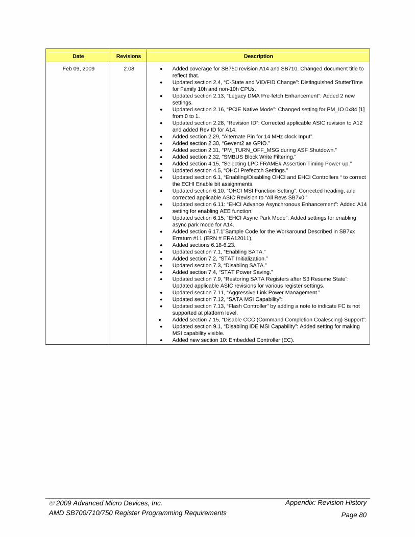
© 2009 Advanced Micro Devices, Inc. Appendix: Revision HistoryAMD SB700/710/750 Register Programming Requirements Page 80
Date Revisions Description
Feb 09, 2009 2.08 • Added coverage for SB750 revision A14 and SB710. Changed document title to reflect that.
• Updated section 2.4, “C-State and VID/FID Change”: Distinguished StutterTime for Family 10h and non-10h CPUs.
• Updated section 2.13, “Legacy DMA Pre-fetch Enhancement”: Added 2 new settings.
• Updated section 2.16, “PCIE Native Mode”: Changed setting for PM_IO 0x84 [1] from 0 to 1.
• Updated section 2.28, “Revision ID”: Corrected applicable ASIC revision to A12 and added Rev ID for A14.
• Added section 2.29, “Alternate Pin for 14 MHz clock Input”. • Added section 2.30, “Gevent2 as GPIO.” • Added section 2.31, “PM_TURN_OFF_MSG during ASF Shutdown.” • Added section 2.32, “SMBUS Block Write Filtering.” • Added section 4.15, “Selecting LPC FRAME# Assertion Timing Power-up.” • Updated section 4.5, “OHCI Prefectch Settings.” • Updated section 6.1, “Enabling/Disabling OHCI and EHCI Controllers “ to correct
the ECHI Enable bit assignments. • Updated section 6.10, “OHCI MSI Function Setting”: Corrected heading, and
corrected applicable ASIC Revision to “All Revs SB7x0.” • Updated section 6.11: “EHCI Advance Asynchronous Enhancement”: Added A14
setting for enabling AEE function. • Updated section 6.15, “EHCI Async Park Mode”: Added settings for enabling
async park mode for A14. • Added section 6.17.1”Sample Code for the Workaround Described in SB7xx
Erratum #11 (ERN # ERA12011). • Added sections 6.18-6.23. • Updated section 7.1, “Enabling SATA.” • Added section 7.2, “STAT Initialization.” • Updated section 7.3, “Disabling SATA.” • Added section 7.4, “STAT Power Saving.” • Updated section 7.9, “Restoring SATA Registers after S3 Resume State”:
Updated applicable ASIC revisions for various register settings. • Updated section 7.11, “Aggressive Link Power Management.” • Updated section 7.12, “SATA MSI Capability”: • Updated section 7.13, “Flash Controller” by adding a note to indicate FC is not
supported at platform level. • Added section 7.15, “Disable CCC (Command Completion Coalescing) Support”: • Updated section 9.1, “Disabling IDE MSI Capability”: Added setting for making
MSI capability visible. • Added new section 10: Embedded Controller (EC).