Embed Size (px)
Citation preview

AMD RS880 ASIC Family BIOS Developer’s Guide
For the RS880, RS880D, RS880P, RS880M, RS880MC, RX881 and RS785E
Technical Reference ManualRev. 3.01
P/N: 46143_rs880_bdg_pub_3.01© 2010 Advanced Micro Devices, Inc.

Trademarks
AMD, the AMD Arrow logo, AMD Athlon, ATI, Mobility, PowerPlay, CrossFire, Radeon, and combinations thereof, are trademarks of Advanced Micro Devices, Inc.
HyperTransport is a licensed trademark of the HyperTransport Technology Consortium.
Microsoft and Windows are registered trademarks of Microsoft Corporation.
PCI Express is a registered trademark and PCIe is a trademark of the PCI-Special Interest Group (PCI-SIG).
Other product names used in this publication are for identification purposes only and may be trademarks of their respective companies.
Disclaimer
The contents of this document are provided in connection with Advanced Micro Devices, Inc. ("AMD") products. AMD makes no representations or warranties with respect to the accuracy or completeness of the contents of this publication and reserves the right to make changes to specifications and product descriptions at any time without notice. No license, whether express, implied, arising by estoppel, or otherwise, to any intellectual property rights are granted by this publication. Except as set forth in AMD's Standard Terms and Conditions of Sale, AMD assumes no liability whatsoever, and disclaims any express or implied warranty, relating to its products including, but not limited to, the implied warranty of merchantability, fitness for a particular purpose, or infringement of any intellectual property right.
AMD's products are not designed, intended, authorized or warranted for use as components in systems intended for surgical implant into the body, or in other applications intended to support or sustain life, or in any other application in which the failure of AMD's product could create a situation where personal injury, death, or severe property or environmental damage may occur. AMD reserves the right to discontinue or make changes to its products at any time without notice.
© 2010 Advanced Micro Devices, Inc. All rights reserved.
Table of Contents
Chapter 1: Introduction
1.1 About This Document .........................................................................................................................................................1-1
1.2 Architecture Overview ........................................................................................................................................................1-1
Chapter 2: Register Space Access
2.1 PCIe® Core/Port Indirect Register Space (PCIEIND) .......................................................................................................2-1
2.2 PCIe® Port Indirect Register Space (PCIEIND_P) ............................................................................................................2-1
2.3 HTIU Indirect Register Space (HTIUIND) ........................................................................................................................2-1
2.4 MISC Indirect Register Space (MISCIND) ........................................................................................................................2-1
2.5 Clock Configuration Register Space (CLKCONFIG) ........................................................................................................2-2
Chapter 3: IRQ Mapping
3.1 Integrated GFX ...................................................................................................................................................................3-1
3.2 PCIe® Ports ........................................................................................................................................................................3-1
Chapter 4: UMA Size Consideration
4.1 UMA/System Memory Size ................................................................................................................................................4-1
Chapter 5: CIMX RS880 Architecture
5.1 Introduction .........................................................................................................................................................................5-1
5.2 Distribution Model ..............................................................................................................................................................5-1
5.3 Integration and Usage Model ..............................................................................................................................................5-1
5.4 Flow Chart...........................................................................................................................................................................5-2
5.5 Binary File...........................................................................................................................................................................5-35.5.1 Overview ..............................................................................................................................................................5-35.5.2 Binary Header.......................................................................................................................................................5-3
5.6 CIM Interface Calls Environment ......................................................................................................................................5-4
5.7 Interface Definition .............................................................................................................................................................5-45.7.1 Northbridge Power-On/Reset Initialization..........................................................................................................5-45.7.2 Northbridge HT Initialization...............................................................................................................................5-55.7.3 Northbridge PCIe® Early Initialization ...............................................................................................................5-65.7.4 Northbridge Start Post Initialization...................................................................................................................5-105.7.5 Northbridge Mid-Post Initialization ...................................................................................................................5-145.7.6 Northbridge PCIe Late Post Initialization ..........................................................................................................5-155.7.7 Northbridge Late Post Initialization ...................................................................................................................5-155.7.8 Northbridge PCIe® S3 Resume Initialization ....................................................................................................5-155.7.9 Northbridge S3 Resume Initialization ................................................................................................................5-165.7.10 Northbridge Register Restrictions ......................................................................................................................5-16
5.8 Callback Interface Definition ............................................................................................................................................5-165.8.1 PCIE OEM Callback “CIMCB_PCIE_SLOT_RESET_DEASSERT”..............................................................5-165.8.2 PCIE OEM Callback “CIMCB_PCIE_SLOT_RESET_ASSERT” ...................................................................5-165.8.3 PCIE OEM Callback “CIMCB_PCIE_SLOT_RESET_SUPPORT” ................................................................5-175.8.4 PCIE OEM Callback ”CIMCB_PCIE_TRAINING_COMPLETE”..................................................................5-175.8.5 NB OEM Callback ”CIMCB_NB_UMA_STATE”...........................................................................................5-175.8.6 NB OEM Callback ”CIMCB_NB_GET_VBIOS”.............................................................................................5-185.8.7 NB OEM Callback ”CIMCB_NB_UPDATE_INTEGRATED_INFO” ............................................................5-185.8.8 NB OEM Callback “CIMCB_NB_DDI_COMMEN” .......................................................................................5-18
© 2010 Advanced Micro Devices, Inc. 46143 AMD RS880 ASIC Family BIOS Developer’s Guide 3.00Table of Contents-1
Table of Contents
5.9 Integrated Info Table ........................................................................................................................................................ 5-195.9.1 Overview............................................................................................................................................................ 5-195.9.2 Voltage Control ................................................................................................................................................. 5-19
5.10 CIMx RS880 Directory Structure .................................................................................................................................. 5-195.10.1 Directory Structure Description......................................................................................................................... 5-21
Chapter 6: SurroundViewTM Feature
6.1 SurroundViewTM Feature (Dual Display) ........................................................................................................................ 6-1
Chapter 7: Power Management
7.1 Sx State Power Management............................................................................................................................................. 7-17.1.1 Register Restoration............................................................................................................................................. 7-17.1.2 Resume from S3 State ......................................................................................................................................... 7-2
7.2 S3 PCIe® Graphics BAR Save/Restore Issue Workaround .............................................................................................. 7-27.2.1 BAR Restoration Process and Architecture......................................................................................................... 7-27.2.2 Post Time ............................................................................................................................................................. 7-27.2.3 When Entering S3................................................................................................................................................ 7-37.2.4 When Resuming from S3..................................................................................................................................... 7-3
Chapter 8: Dynamic HyperTransportTM Link Width
8.1 CIMx Support..................................................................................................................................................................... 7-1
8.2 Expanded NBCFG Structure .............................................................................................................................................. 7-1
8.3 CIMx Dynamic Link Width SMI Handler ......................................................................................................................... 7-28.3.1 Dynamic Link Width SMI Requests.................................................................................................................... 7-2
8.4 Northbridge Register Restrictions ...................................................................................................................................... 7-3
Appendix A: Revision History
46143 AMD RS880 ASIC Family BIOS Developer’s Guide 3.00 © 2010 Advanced Micro Devices, Inc.Table of Contents-2

List of Figures
© 2010 Advanced Micro Devices, Inc. 46143 AMD RS880 ASIC Family BIOS Developer’s Guide 3.00List of Figures-1
List of Figures
Figure 5-1: Integration and Usage Model ...................................................................................................................................... 5-1Figure 5-2: RS880 Flow Chart ....................................................................................................................................................... 5-2Figure 5-3: CIMX-RS880 Binary File Format ............................................................................................................................... 5-3Figure 5-4: CIMx RS880 Directory Structure .............................................................................................................................. 5-20
List of Tables
© 2010 Advanced Micro Devices, Inc. 46143 AMD RS880 ASIC Family BIOS Developer’s Guide 3.00List of Tables-1
List of Tables
Table 3-1: Integrated GFX Device Bit Setting ................................................................................................................................3-1Table 3-2: PCIe® Ports Device Bit Settings ...................................................................................................................................3-1Table 4-1: UMA/System Memory Size ..........................................................................................................................................4-1Table 5-1: CIM File Header Definition ...........................................................................................................................................5-3Table 5-2: Northbridge Power-On/Reset Initialization ...................................................................................................................5-4Table 5-3: htConfiguration ..............................................................................................................................................................5-5Table 5-4: eConfiguration ...............................................................................................................................................................5-7Table 5-5: lConfiguration ................................................................................................................................................................5-7Table 5-6: PortFeatures[11] ............................................................................................................................................................5-8Table 5-7: GPPConfig .....................................................................................................................................................................5-9Table 5-8: GFXConfig ....................................................................................................................................................................5-9Table 5-9: nbConfiguration ...........................................................................................................................................................5-11Table 5-10: gfxConfiguration ........................................................................................................................................................5-11Table 5-11: spConfiguration .........................................................................................................................................................5-12Table 5-12: DhlwConfiguration ....................................................................................................................................................5-13Table 5-13: CState .........................................................................................................................................................................5-14
Chapter 1Introduction
1.1 About This Document
This manual contains guidelines for the BIOS and software development of a system that utilizes the RS880 family of IGPs. Unless indicated otherwise, the programming information in this document applies to the following RS880 ASIC variants:
• RS880• RS880D• RS880P• RS880M• RS880MC• RX881• RS785E
Changes and additions to the previous release of this document are highlighted in red. Refer to Appendix A at the end of this document for a detailed revision history.
1.2 Architecture Overview
The RS880 is a high performance system logic chip that supports the simultaneous operation of two external PCI Express® graphics cards on an AMD Sempron/Athlon 64/Athlon 64 FX/Rev 10/Rev 11 platform. It supports a four-lane PCI Express interface to the AMD IXP, as well as six ports for external PCI Express devices.
AMD’s RS880 provides a bridge between HyperTransportTM and PCI Express. Both HyperTransport and PCI Express are point-to-point connections. Using point-to-point connections allows much higher bandwidth than that with a shared bus (such as PCI) since the electrical design can be controlled much better. From a software perspective, both HyperTransport and PCI Express are compatible with PCI configuration mechanisms.
© 2010 Advanced Micro Devices, Inc. 46143 AMD RS880 ASIC Family BIOS Developer’s Guide 3.001-1

Architecture Overview
This page is left blank intentionally.
46143 AMD RS880 ASIC Family BIOS Developer’s Guide 3.00 © 2010 Advanced Micro Devices, Inc.1-2
Chapter 2Register Space Access
2.1 PCIe® Core/Port Indirect Register Space (PCIEIND)
The Core Index Space contains control and status registers that are generic to all PCIe® ports in the RS880. This register space is accessed through the following index/data register pair located in the RS880’s northbridge PCI configuration registers:
• Index register is bus 0, device 0, register 0xE0.
• Data register is bus 0, device 0, register 0xE4.
Note: Register descriptions are referenced with the name PCIEIND.
The Core Index Space is subdivided into two parts. Since there are a total of 3 PCIe cores in the RS880, hardware has been implemented to provide a mechanism to access these registers either independently or jointly through the programming of bits [18:16] of the index register 0xE0. The encoding is as follows:
• 0xE0[18:16] == 0x1: Reads and writes accesses to 0xE4 will be directed at the per-core index registers in PCIE-GPPSB only.
• 0xE0[18:16] == 0x2: Reads and writes accesses to 0xE4 will be directed at the per-core index registers in PCIE-GPP only.
• 0xE0[18:16] == 0x0: Reads and writes accesses to 0xE4 will be directed at the per-core index registers for PCIE-GFX only.
Note: Register descriptions are referenced with the name PCIEIND or BIFNB.
2.2 PCIe® Port Indirect Register Space (PCIEIND_P)
This register space is accessed through the following index/data register pair located in the RS880’s northbridge PCI configuration registers:
• Index register is bus 0, device 2/3/4/5/6/7/9/10, register 0xE0[15..0].
• Data register is bus 0, device 2/3/4/5/6/7/9/10, register 0xE4[31..0].
Note: Register descriptions are referenced with the name PCIEIND_P or BIFNBP.
2.3 HTIU Indirect Register Space (HTIUIND)
This register space is accessed through the following index/data register pair located in the RS880’s northbridge PCI configuration registers:
• Index register is bus 0, device 0, register 0x94[7:0].
• Data register is bus 0, device 0, register 0x98[31:0]. To write HTIUIND, register 0x94[8] has to be set.
Note: Register descriptions are referenced with the name HTIUIND.
2.4 MISC Indirect Register Space (MISCIND)
This register space is accessed through the following index/data register pair located in the RS880’s northbridge PCI configuration registers:
• Index register is bus 0, device 0, register 0x60[7:0].
• Data register is bus 0, device 0, register 0x64[31:0]. To write MISCIND, register 0x60[7] has to be set.
Note: Register descriptions are referenced with the name MISCIND.
© 2010 Advanced Micro Devices, Inc. 46143 AMD RS880 ASIC Family BIOS Developer’s Guide 3.002-1

Clock Configuration Register Space (CLKCONFIG)
2.5 Clock Configuration Register Space (CLKCONFIG)
The RS880 clock control block is located in Device0, Function1. By default, this PCI function does not appear in the PCI configuration space. System firmware can make Device0, Function1 visible by setting NBCONFIG:0x4C[0] to 1. The expected use of the Clock Control function is to only enable it in the PCI configuration space for modification by system firmware during POST. This function does not implement PCI device and vendor ID’s. Therefore, system firmware should hide the Clock Control function after making modifications.
46143 AMD RS880 ASIC Family BIOS Developer’s Guide 3.00 © 2010 Advanced Micro Devices, Inc.2-2
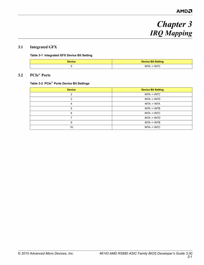
Chapter 3IRQ Mapping
3.1 Integrated GFX
3.2 PCIe® Ports
Table 3-1 Integrated GFX Device Bit Setting
Device Device Bit Setting
5 INTA -> INTC
Table 3-2 PCIe® Ports Device Bit Settings
Device Device Bit Setting
2 INTA -> INTC
3 INTA -> INTD
4 INTA -> INTA
5 INTA -> INTB
6 INTA -> INTC
7 INTA -> INTD
9 INTA -> INTB
10 INTA -> INTC
© 2010 Advanced Micro Devices, Inc. 46143 AMD RS880 ASIC Family BIOS Developer’s Guide 3.003-1

PCIe® Ports
This page is left blank intentionally.
46143 AMD RS880 ASIC Family BIOS Developer’s Guide 3.00 © 2010 Advanced Micro Devices, Inc.3-2
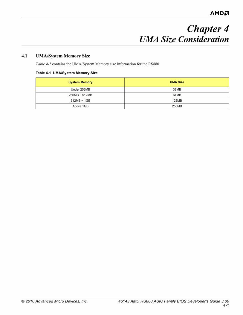
Chapter 4UMA Size Consideration
4.1 UMA/System Memory Size
Table 4-1 contains the UMA/System Memory size information for the RS880.
Table 4-1 UMA/System Memory Size
System Memory UMA Size
Under 256MB 32MB
256MB ~ 512MB 64MB
512MB ~ 1GB 128MB
Above 1GB 256MB
© 2010 Advanced Micro Devices, Inc. 46143 AMD RS880 ASIC Family BIOS Developer’s Guide 3.004-1

UMA/System Memory Size
This page is left blank intentionally.
46143 AMD RS880 ASIC Family BIOS Developer’s Guide 3.00 © 2010 Advanced Micro Devices, Inc.4-2
Chapter 5CIMX RS880 Architecture
5.1 Introduction
The CIMX-RS880 introduces a new interface and distribution model to help quickly integrate RS880 Northbridge family support in the customer products.
5.2 Distribution Model
To avoid miscellaneous build issues and simplify integration with different BIOS code bases, CIMX-RS880 is distributed in the form of binary files called “B1”, “B2” and “B3”. B1 contains minimum initialization required for BIOS recovery, B2 contains full chipset initialization code, and B3 contains SMI code.
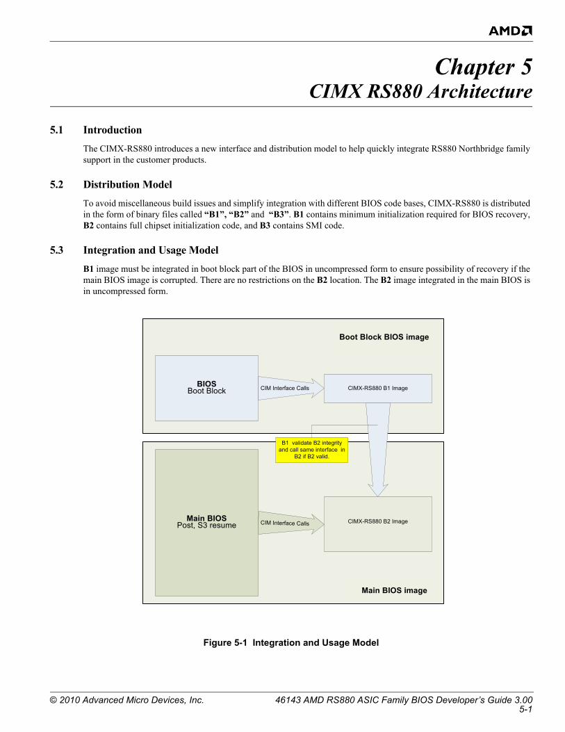
5.3 Integration and Usage Model
B1 image must be integrated in boot block part of the BIOS in uncompressed form to ensure possibility of recovery if the main BIOS image is corrupted. There are no restrictions on the B2 location. The B2 image integrated in the main BIOS is in uncompressed form.
Figure 5-1 Integration and Usage Model
Main BIOSPost, S3 resume
BIOSBoot Block CIMX-RS880 B1 Image
CIMX-RS880 B2 Image CIM Interface Calls
CIM Interface Calls
B1 validate B2 integrity and call same interface in
B2 if B2 valid.
Main BIOS image
Boot Block BIOS image
© 2010 Advanced Micro Devices, Inc. 46143 AMD RS880 ASIC Family BIOS Developer’s Guide 3.005-1
Flow Chart
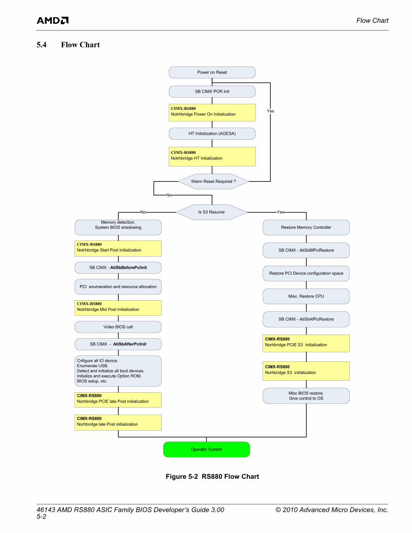
5.4 Flow Chart
Figure 5-2 RS880 Flow Chart
Power on Reset
CIMX-RS880 Notrhbridge HT Initialization
SB CIMX POR Init
Memory detection.System BIOS shadowing
Is S3 Resume
Restore Memory Controller
Restore PCI Device configuration space
Misc. Restore CPU
CIMX-RS880 Norhbridge S3 initialization
Misc BIOS restore.Give control to OS
Operatin System
CIMX-RS880 Notrhbridge Start Post Initialization
SB CIMX - AtiSbBeforePciInit
PCI enumeration and resource allocation
Video BIOS call
SB CIMX - AtiSbAfterPciInit
Cnfigure all IO device.Enumerate USB.Detect and initialize all boot devices.Initialize and execute Option ROM.BIOS setup, etc
CIMX-RS880Norhbridge late Post initialization
YesNo
CIMX-RS880Norhbridge PCIE late Post initialization
SB CIMX - AtiSbBfPciRestore
SB CIMX - AtiSbAfPciRestore
HT Initialization (AGESA)
Warm Reset Required ?
CIMX-RS880 Notrhbridge Power On Initialization
CIMX-RS880Norhbridge PCIE S3 initialization
Yes
No
CIMX-RS880 Notrhbridge Mid Post Initialization
46143 AMD RS880 ASIC Family BIOS Developer’s Guide 3.00 © 2010 Advanced Micro Devices, Inc.5-2
Binary File
5.5 Binary File
5.5.1 Overview
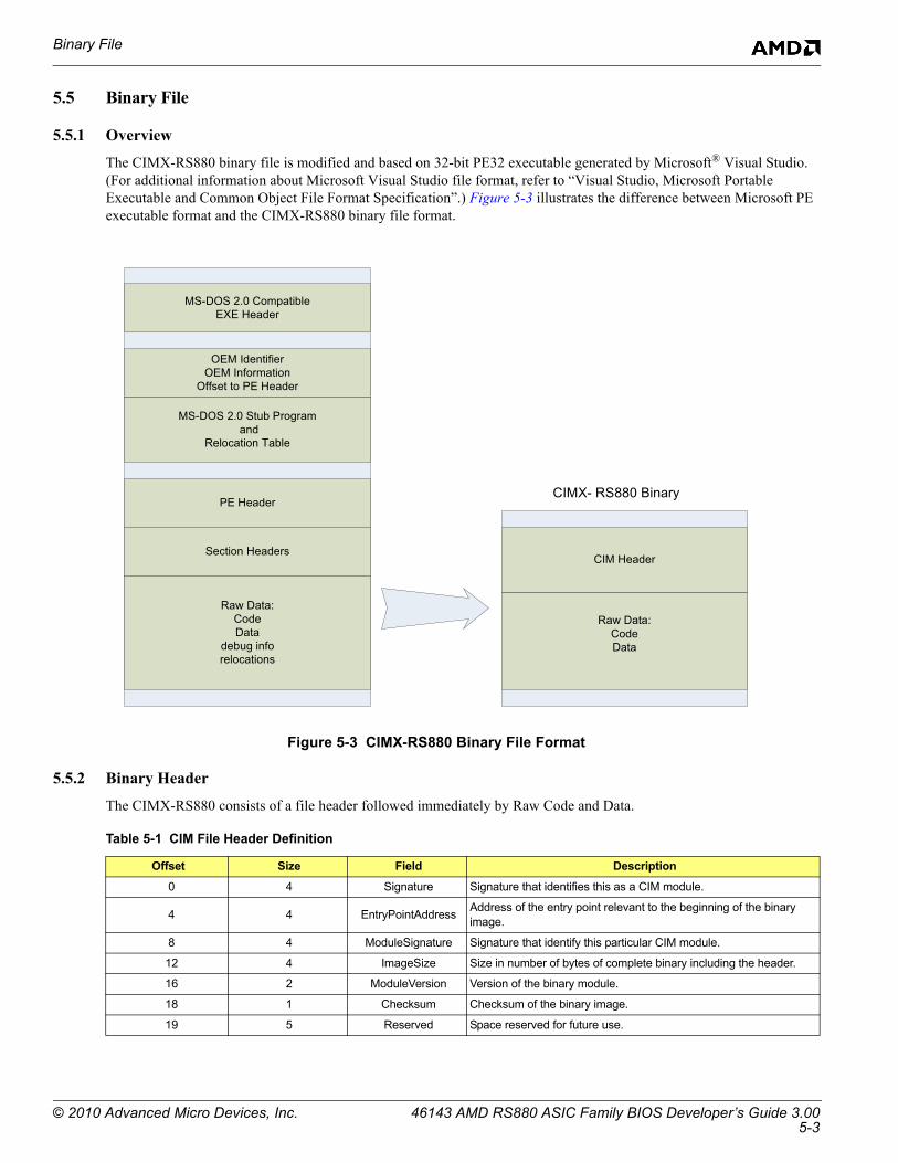
The CIMX-RS880 binary file is modified and based on 32-bit PE32 executable generated by Microsoft® Visual Studio. (For additional information about Microsoft Visual Studio file format, refer to “Visual Studio, Microsoft Portable Executable and Common Object File Format Specification”.) Figure 5-3 illustrates the difference between Microsoft PE executable format and the CIMX-RS880 binary file format.
Figure 5-3 CIMX-RS880 Binary File Format
5.5.2 Binary Header
The CIMX-RS880 consists of a file header followed immediately by Raw Code and Data.
Table 5-1 CIM File Header Definition
Offset Size Field Description
0 4 Signature Signature that identifies this as a CIM module.
4 4 EntryPointAddress Address of the entry point relevant to the beginning of the binary image.
8 4 ModuleSignature Signature that identify this particular CIM module.
12 4 ImageSize Size in number of bytes of complete binary including the header.
16 2 ModuleVersion Version of the binary module.
18 1 Checksum Checksum of the binary image.
19 5 Reserved Space reserved for future use.
MS-DOS 2.0 CompatibleEXE Header
OEM IdentifierOEM Information
Offset to PE Header
PE Header
Section Headers
MS-DOS 2.0 Stub Program and
Relocation Table
Raw Data:CodeData
CIM Header
CIMX- RS880 Binary
Raw Data:CodeData
debug inforelocations
© 2010 Advanced Micro Devices, Inc. 46143 AMD RS880 ASIC Family BIOS Developer’s Guide 3.005-3
CIM Interface Calls Environment
5.6 CIM Interface Calls Environment
Prior to calling any CIMX interface, it is required that the following steps be performed:
• Step 1: Place CPU into 32-bit protected mode.
• Step 2: Set CS as 32-bit code segment with Base/Limit – 0x00000000/0xffffffff.
• Step 3: Set DS/ES/SS as 32-bit data segment with Base/Limit – 0x00000000/0xffffffff.
See section 5.10 for a programming example.
5.7 Interface Definition
All interface calls to the CIMX-RS880 binary are C-like calls to the Entry Point of the binary image:
void (*ImageEntryPointPtr)(void* Config)
5.7.1 Northbridge Power-On/Reset Initialization
Upon system power-on or cold reset, the RS880 is supposed to be self-initialized to a working state without any software interference. However, the CIM may need to program the recommended settings for the purpose of enabling special functions and performance improvement during early initialization.
Functions Documentation:
void (*ImageEntryPointPtr)(STDCFG * Config)
Detail Description:
stdHeader: Standard function callstdHeader.Func = 0x1
typedef struct _STDCFG{UINT32 pImageBase;UINT32 pPcieBase;UINT8 Func;UINT32 pCallBack;UINT32 pB2ImageBase;
}STDCFG;
pImageBase: Physical 32-bit address of binary image location.pPcieBase: Address of PCIE Extended Configuration Space MMIO. It is required that the PCIE MMIO range be programmed in the CPU Memory Mapped IO Base/Limit registers.
Func: Function identifier.pCallBack: Address of OEM callback function.pB2ImageBase: Optional parameter. Physical 32-bit address of “B2” image location.
Table 5-2 Northbridge Power-On/Reset Initialization
Bit Field Description
[7:0] PCIE Extended Configuration sizeSize of PCIE Extended Configuration Space in MB. 0 – 256MB for backward compatibility.
[31:20] PCIE Extended Configuration Base [31:20] of PCIE Extended Configuration Base address.
Example:0xE0000000 – PCIE Extended Cfg. MMIO 0xE0000000 – 0xEFFFFFFF (256MB) 0xE0000040 – PCIE Extended Cfg. MMIO 0xE0000000 – 0xE3FFFFFF (64MB)
46143 AMD RS880 ASIC Family BIOS Developer’s Guide 3.00 © 2010 Advanced Micro Devices, Inc.5-4
Interface Definition
5.7.2 Northbridge HT Initialization
The RS880 requires additional initialization for HT3 support interface call. It must be executed prior to applying link speed and width, but after HT link is fully speed/width configured on the northbridge and the CPU side.
Functions Documentation:
void (*ImageEntryPointPtr)(HTCFG* Config)
Parameters:
typedef struct _HTCFG{STDCFG stdHeader;void* DebugPtr;UINT32 Status;UINT32 htConfiguration;UINT8 ParentNodeLinkID;UINT8 ParentNodeSubLinkID;UINT32 Reserved;UINT16 HTRefClkMHz;UINT8 NBDeemphasiesLevel;UINT8 Reserved1;UINT64 Reserved2;UINT64 Reserved3;
}HTCFG;
Detail Description:
stdHeader: Standard function call (see STDCFG definition)stdHeader.Func = 0x2
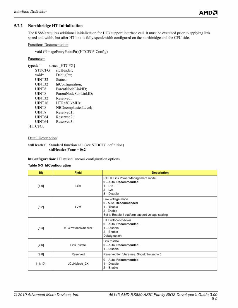
htConfiguration: HT miscellaneous configuration options
Table 5-3 htConfiguration
Bit Field Description
[1:0] LSx
RX HT Link Power Management mode0 – Auto. Recommended1 – L1s2 – L2s3 – Disable
[3:2] LVM
Low voltage mode0 - Auto. Recommended1 - Disable2 - EnableSet to Enable if platform support voltage scaling
[5:4] HT3ProtocolChecker
HT Protocol checker0 – Auto. Recommended1 – Disable2 – EnableDebug option.
[7:6] LinkTristateLink tristate0 – Auto. Recommended1 – Disable
[9:8] Reserved Reserved for future use. Should be set to 0.
[11:10] LCLKMode_2X0 – Auto. Recommended1 – Disable2 – Enable
© 2010 Advanced Micro Devices, Inc. 46143 AMD RS880 ASIC Family BIOS Developer’s Guide 3.005-5
Interface Definition
ParentNodeLinkID: Parent node HT Link ID to which RS880 is connected (0, 1, 2, 3)ParentNodeSubLinkID: Parent node HT Sub Link ID to which RS880 is connected:
(0,1) If the link is unganged. (0) If the link is ganged.
HTRefClkMHz: HT reference clock in MHz. Acceptable range: 200MHz - 450MHz. All other values are treated as 200MHz.DebugPtr: Pointer to extended HT debug feature. Recommended setting is 0.Status: Status returned by this interface call (TBD).NBDeemphasiesLevel: Acceptable values: 0 = Disabled, 1 = 2dB, 2 = 3dB, 3 = 6dB, 4 = 9dB. The De-emphasis settings should be based on the PCB trace length between the chipset and the processor. Refer to RS880 RPR for the current table.
5.7.3 Northbridge PCIe® Early Initialization
The RS880 requires initialization of the PCIe® block (Ports and Device) prior to PCI bus enumeration and resource allocation. The CIM may also need to program the recommended settings for the purpose of enabling special functions and for performance improvement during PCIe early initialization.
Functions Documentation:
void (*ImageEntryPointPtr)(PCICFG* Config)
Parameters:
typedef struct _PCICFG{STDCFG StdHeader;void* DebugPtr;UINT32 Status;UINT32 eConfiguration;UINT32 lConfiguration;PORTCFG PortFeatures[11];UINT32 TempMMIO;UINT8 GPPConfig;UINT8 GFXConfig;UINT32 BroadcastBase;UINT32 BroadcastSize;UINT16 DelayTraining;UINT32 Reserved1;UINT64 Reserved2;UINT64 Reserved3;
}PCICFG;
Callbacks:
PCIE OEM callback “CIMCB_PCIE_SLOT_RESET_DEASSERT” (see section 5.8.1)
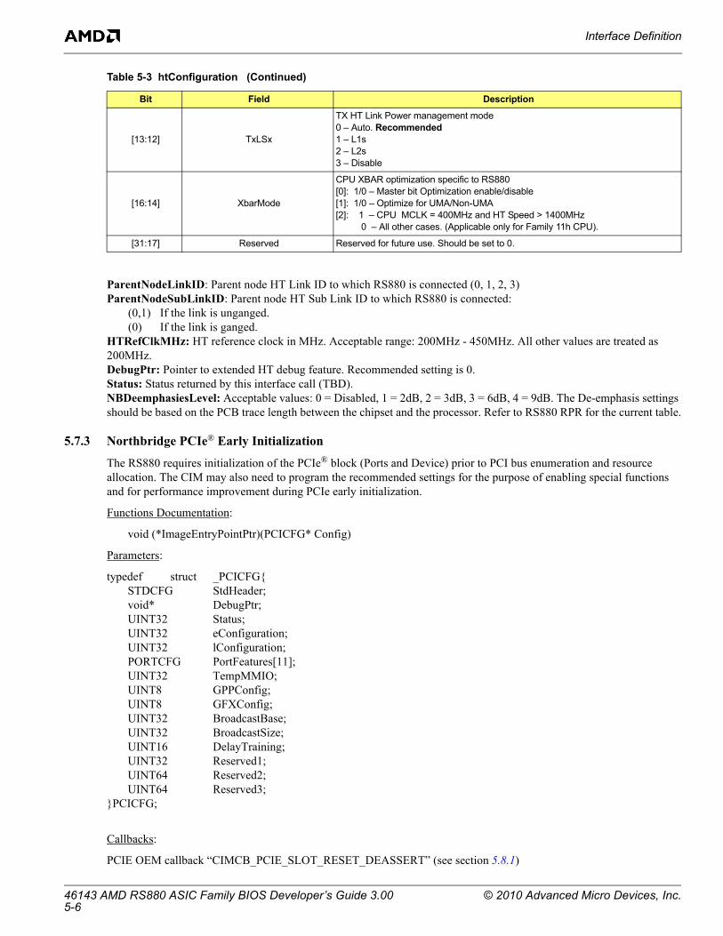
[13:12] TxLSx
TX HT Link Power management mode0 – Auto. Recommended1 – L1s2 – L2s3 – Disable
[16:14] XbarMode
CPU XBAR optimization specific to RS880[0]: 1/0 – Master bit Optimization enable/disable[1]: 1/0 – Optimize for UMA/Non-UMA[2]: 1 – CPU MCLK = 400MHz and HT Speed > 1400MHz 0 – All other cases. (Applicable only for Family 11h CPU).
[31:17] Reserved Reserved for future use. Should be set to 0.
Table 5-3 htConfiguration (Continued)
Bit Field Description
46143 AMD RS880 ASIC Family BIOS Developer’s Guide 3.00 © 2010 Advanced Micro Devices, Inc.5-6
Interface Definition
PCIE OEM callback “CIMCB_PCIE_SLOT_RESET_ASSERT” (section 5.8.2)PCIE OEM callback “CIMCB_PCIE_SLOT_RESET_SUPPORT” (section 5.8.3)PCIE OEM callback “CIMCB_PCIE_TRAINING_COMPLETE” (section 5.8.4)
Detail Description:
stdHeader: Standard function call (see STDCFG definition)stdHeader.Func = 0x3
eConfiguration: PCIE Miscellaneous Configuration options
lConfiguration: PCIE Miscellaneous Configuration options.
Table 5-4 eConfiguration
Bit Field Description
[0]PCIE_GFX_LANE_REVERSAL Lanes reversal configuration for GFX slots (DEV 2/3). The value is Platform specific.
0 – Disable1 – Enable
[1] Reserved Must be set to 0.
[3:2] Reserved Must be set to 0.
[5:4]PCIE_REFCLK_MODE Select reference clock mode for GFX PCIE core.
[4] – 1 Use SB REFCLK for GFX REFCLK, 0 – use external REFCLK for GFX.[5] – 1 - Use SB REFCLK for GPP REFCLK, 0 – use external REFCLK for GPP.
[6]PCIE_GFX_WORKAROUND_DIS Misc. GFX cards (ATI/NV) workaround.
0 – Enable. Recommended.1 – Disable.
[7]PCIE_GFX_LANEPOWEROFF_DIS Unused lanes power off for GFX/GFX2.
0 – Enable. Recommended. 1 – Disable.
[8]PCIE_GPP_LANEPOWEROFF_DIS Unused lanes power off for GPP.
0 – Enable. Recommended. 1 – Disable.
[12:9] Reserved Must be set to 0.
[14:13] Reserved Must be set to 0.
[15] Reserved Must be set to 0.
[16]PCIE_LPC_DEADLOCK_WRK_DIS LPC deadlock workaround.
0 – Enable. Recommended. 1 – Disable.
[18:17]
PCIE_CPL_BUFF_ALLOC Slave CPL buffer allocation.0 – Auto. Recommended.1 – Disable.2 – Enable
[19]PCIE_OVERCLOCKING PCIE REFCLKC is overclocked.
0- Non overlcocked. Recommended. 1 – Overclocked.
[20]PCIE_GPP2_CONFIG PCIE GPP core configuration.
0 – Dev9 – x1, Dev10 – x11 – Dev9 – x2
[21]PCIE_NB_SB_HALF_SWING NB-SB Link Half Swing mode. This feature is applicable for mobile designs with trace
lengths of ~1 cm between the NB and the SB.
Table 5-5 lConfiguration
Bit Field Description
[1:0]
PCIE_GFX_TX_GATING Control GFX core TX clock gating0 – Auto. Recommended.1 – Disable.2 – Enable.
[3:2] Reserved Must be set to 0.
© 2010 Advanced Micro Devices, Inc. 46143 AMD RS880 ASIC Family BIOS Developer’s Guide 3.005-7
Interface Definition
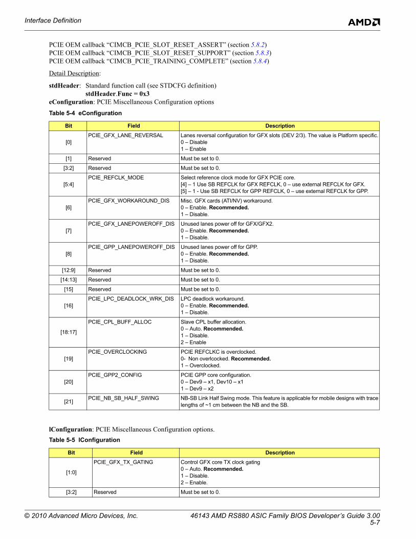
PortFeatures[11]: Per PCIE Port Configuration options. (PortFeatures[2] – DEV 2, PortFeatures[3] – DEV 3,…,) PortFeatures[10]: DEV 10, PortFeatures[0]/PortFeatures[1] – Reserved for future use).
[5:4] PCIE_GFX_PLL_CONTROL Debug option. Should be set to 0
[7:6] Reserved Must be set to 0.
[9:8] PCIE_GPP_PLL_CONTROL Debug option. Should be set to 0
[10..11]
PCIE_GFX_LCLK_GATING Control GFX core LCLK clock gating0 – Auto. Recommended.1 – Disable.2 – Enable.
[13:12] Reserved Must be set to 0.
[15:14]
PCIE_GPP_TX_GATING Control GPP Core TX clock gating0 – Auto. Recommended.1 – Disable.2 – Enable.
[17:16]
PCIE_SB_TX_GATING Control SB Core TX clock gating0 – Auto. Recommended.1 – Disable.2 – Enable.
[19:18]
PCIE_GPP_LCLK_GATING Control GPP Core LCLK clock gating0 – Auto. Recommended.1 – Disable.2 – Enable.
[21:20]
PCIE_SB_LCLK_GATING Control SB Core LCLK clock gating0 – Auto. Recommended.1 – Disable.2 – Enable.
[23:22]
PCIE_NB_SB_VC Enable Non-Posted VC1 traffic on NB-SB link.0 – Auto. Recommended.1 – Disable.2 – Enable.
[24]PCIE_DESKTOP_POWERMANAGEMENT_DIS
Debug option. Should be set to 0.0 – Do not disable. Recommended.1 – Disable.
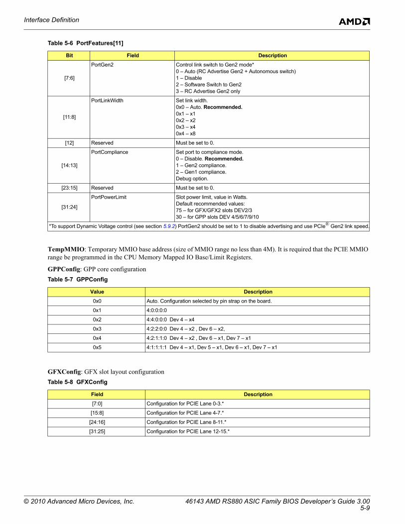
Table 5-6 PortFeatures[11]
Bit Field Description
[0]PortPresent Slot presence for PCIe® port.
0 – Not present1 – Present.
[1]
PortDetect Endpoint detection. For internal use. Filled by CIM.1 – Detected.0 – Not detected.Should be set to 0 on CIM module call.
[2] Reserved Reserved for future use. Should be set to 0.
[3]PortHotPlug Port hotplug control.
0 – Port does not support hotplug.1 – Port supports hotplug.
[5:4]
PortAspm Enable ASPM.0x0 – Disable. 0x1 – Enable L0s.0x2 – Enable L10x3 – Enable L0s and L1.
Table 5-5 lConfiguration (Continued)
Bit Field Description
46143 AMD RS880 ASIC Family BIOS Developer’s Guide 3.00 © 2010 Advanced Micro Devices, Inc.5-8
Interface Definition
TempMMIO: Temporary MMIO base address (size of MMIO range no less than 4M). It is required that the PCIE MMIO range be programmed in the CPU Memory Mapped IO Base/Limit Registers.
GPPConfig: GPP core configuration
GFXConfig: GFX slot layout configuration
[7:6]
PortGen2 Control link switch to Gen2 mode*0 – Auto (RC Advertise Gen2 + Autonomous switch)1 – Disable2 – Software Switch to Gen23 – RC Advertise Gen2 only
[11:8]
PortLinkWidth Set link width. 0x0 – Auto. Recommended.0x1 – x10x2 – x20x3 – x40x4 – x8
[12] Reserved Must be set to 0.
[14:13]
PortCompliance Set port to compliance mode.0 – Disable. Recommended.1 – Gen2 compliance. 2 – Gen1 compliance.Debug option.
[23:15] Reserved Must be set to 0.
[31:24]
PortPowerLimit Slot power limit, value in Watts. Default recommended values:75 – for GFX/GFX2 slots DEV2/3 30 – for GPP slots DEV 4/5/6/7/9/10
*To support Dynamic Voltage control (see section 5.9.2) PortGen2 should be set to 1 to disable advertising and use PCIe® Gen2 link speed.
Table 5-7 GPPConfig
Value Description
0x0 Auto. Configuration selected by pin strap on the board.
0x1 4:0:0:0:0
0x2 4:4:0:0:0 Dev 4 – x4
0x3 4:2:2:0:0 Dev 4 – x2 , Dev 6 – x2,
0x4 4:2:1:1:0 Dev 4 – x2 , Dev 6 – x1, Dev 7 – x1
0x5 4:1:1:1:1 Dev 4 – x1, Dev 5 – x1, Dev 6 – x1, Dev 7 – x1
Table 5-8 GFXConfig
Field Description
[7:0] Configuration for PCIE Lane 0-3.*
[15:8] Configuration for PCIE Lane 4-7.*
[24:16] Configuration for PCIE Lane 8-11.*
[31:25] Configuration for PCIE Lane 12-15.*
Table 5-6 PortFeatures[11]
Bit Field Description
© 2010 Advanced Micro Devices, Inc. 46143 AMD RS880 ASIC Family BIOS Developer’s Guide 3.005-9
Interface Definition
BroadcastBase: Broadcast MMIO is required for the CrossFireTM mode. This memory mapped IO must be reserved and not used for any other purpose. It must be appropriately reported to OS as reserved.BroadcastSize: Broadcast MMIO size in bytes.DelayTraining: Delay training after deassert port reset (in ms). 2 ms is recommended delay.
5.7.4 Northbridge Start Post Initialization
The RS880 requires initialization of top of memory to enable DMA to system memory. The CIM also may need to program the recommended settings for the purpose of enabling special functions and performance improvement during early initialization. It is mandatory to use the same copy of NBCFG between Start post, Mid post, Late post, and S3 resume initialization. This will allow CIM to exchange data between interface calls if necessary.
Functions Documentation:
void (*ImageEntryPointPtr)(NBCFG* Config)
Parameters:
typedef struct _NBCFG{STDCFG stdHeader;void* DebugPtr;UINT32 Status;UINT32 nbConfiguration;UINT32 gfxConfiguration;UINT32 spConfiguration;UINT16 UMABase;UINT16 UMASize;UINT16 SysMemTomLo;UINT16 SysMemTomHi;UINT16 MCLK;UINT16 ECLK;SPTBLHEADER* spOemInitTablePtr;UINT8 CState;UINT32 SSID;UINT32 APCSSID;UINT32 GFXSSID;
*GFXConfig [x..y] = 0x0 – Auto. (If slot present is enabled on Port 2 only, then all lanes belong to Port A; if slot present is enabled on Port 3 only, then lanes 8 to 15 belong to Port B; if slot present is enabled on both Port 2 and Port 3, then lanes 0 to 7 belong to Port A and lanes 8 to 15 belong to Port B).
GFXConfig [x..y] = 0x80 – Lanes unused
GFXConfig [x..y] [3:0] – Lane Type 0x01 – Lane Type Port A 0x02 – Lane Type Port B 0x04 – Lane Type DDI1 0x08 – Lane Type DDI2GFXConfig [x..y] [5:4] – Connector Type 0x00 – Single Link DVI 0x01 – Dual Link DVI 0x02 – HDMI 0x03 – Display PortGFXConfig [x..y] [7:5] – Misc Config (Mobile design with DDI) 0x00 – DDI in Docking Station and Undocking case 0x01 – DDI out of Docking Station 0x02 – DDI in Docking Station
Table 5-8 GFXConfig (Continued)
Field Description
46143 AMD RS880 ASIC Family BIOS Developer’s Guide 3.00 © 2010 Advanced Micro Devices, Inc.5-10
Interface Definition
UINT32 AUDIOSSID;UINT8 ParentNodeLinkID;UINT8 ParentNodeSubLinkID;UINT16 AllPcieGfxInfo;UINT16 AmdPcieGfxInfo;UINT16 PrivateNBVoltage;UINT16 PrivateNumberOfCyclesInPeriod;HTLWBITCFG DhlwConfiguration;UINT16 DhlwSmiPort;UINT16 DhlwPrivateStatus;UINT64 Reserved3;
}NBCFG;
Callbacks:
NB OEM callback ”CIMCB_NB_UMA_STATE” (section 5.8.5)
Detail Description:
stdHeader: Standard function call (see STDCFG definition)stdHeader.Func = 0x4
nbConfiguration: NB miscellaneous configuration options
gfxConfiguration: Miscellaneous GFX configuration.
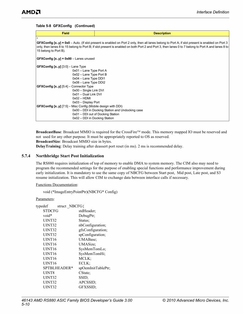
Table 5-9 nbConfiguration
Bit Field Description
[2:0] UnitIDClampConfig
UnitID clumping to increase the number of outstanding requests supported by a single device.
0 – Auto. Recommended. 1 – Disable.2 – Unit ID clump for PCIE 3 – Unit ID clump for GFX4 – Unit ID clump for PCIE & GFX
[4:3] NBPowerManagment
Misc NB power management features.
0 – Auto. Recommended. 1 – Disable.2 – Enable.
[5] SetUpCpuMMIO
Set up CPU MMIO
0 – Disable (Platform BIOS sets up MMIO)1 – Enable. Recommended
Table 5-10 gfxConfiguration
Bit Field Description
[0] UMA_ENABLEUMA mode.1 – Enable
[1] SP_ENABLESidePort memory support.1 – EnableSee Note.
[2] AUDIO_ENABLEHD Audio support.1 – Enable; Recommended.
[3] SVIEW_ENABLESurround View support.1 – Enable
© 2010 Advanced Micro Devices, Inc. 46143 AMD RS880 ASIC Family BIOS Developer’s Guide 3.005-11
Interface Definition
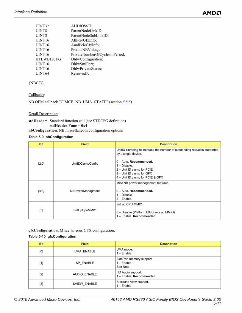
spConfiguration: Miscellaneous sideport memory/configuration.
[4] FORCE_IGFX_ENABLEForce enable internal GFX regardless external GFX presence. Debug options. Recommended to be set to 0.
[7:5] Reserved
[8] ADD2_CARD_AUTODETECT Enables the detection for ADD2 style DDI card.
[9..10] Reserved
[11..12] SpCalibration
Side Port Memory Calibration Type00 – Calibration Disabled 01 – Read calibration only10 – Write calibration only11 – Read and write calibration (Recommended default setting)
[13..15] AdjustEighth
Side Port Memory Calibration Parameter000 – Auto (Recommended default setting)001 – Reserved010 – Use 2/8 value for calibration011 – Use 3/8 value for calibration100 – Use 4/8 value for calibration101 – Use 5/8 value for calibration110 – Use 6/8 value for calibration111 - Reserved
Note: Only two internal GFX modes support UMA Only and UMA+SP. If SP_ENABLE is set to 1, then UMA_ENABLE must also be set to 1.
Table 5-11 spConfiguration
Bit Field Description
[5:0] InterleaveRatio
SP/UMA memory interleave ratio.0 - Auto. Recommended. (Actual ratio will be determined after RS880 performance tuning);1 – 1:12 – 1:33 – 1:74 – 1:155 – 3:56 – 3:137 – 5:118 – 7:9
[7:6] InterleaveMode
SP/UMA memory interleave mode.0 - Auto. Recommended.1 – Corse.2 – Fine.
[10:8] SPdynamicCtrl
Misc. SP MC power management.0 - Auto. Recommended.1 – Dynamic CKE2 – Dynamic CMD3 – Dynamic CKE4 – Disabled
[12:11] ControllerTermination
NB termination.0 - Auto. Recommended.1 – Disable2 – Enable
[14:13] MemoryTermination
Memory termination.0 - Auto. Recommended.1 – Disable2 – Enable
Table 5-10 gfxConfiguration (Continued)
Bit Field Description
46143 AMD RS880 ASIC Family BIOS Developer’s Guide 3.00 © 2010 Advanced Micro Devices, Inc.5-12
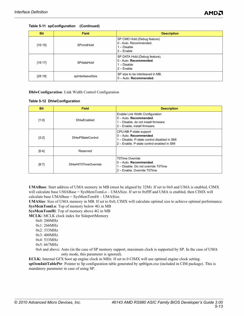
Interface Definition
DhlwConfiguration: Link Width Control Configuration
UMABase: Start address of UMA memory in MB (must be aligned by 32M). If set to 0x0 and UMA is enabled, CIMX will calculate base UMABase = SysMemTomLo – UMASize. If set to 0xffff and UMA is enabled, then CIMX will calculate base UMABase = SysMemTomHi – UMASize.UMASize: Size of UMA memory in MB. If set to 0x0, CIMX will calculate optimal size to achieve optimal performance.SysMemTomLo: Top of memory below 4G in MBSysMemTomHi: Top of memory above 4G in MBMCLK: MCLK clock index for SideportMemory
0x0: 200MHz0x1: 266MHz0x2: 333MHz0x3: 400MHz0x4: 533MHz0x5: 667MHz0x6 and above: Auto (in the case of SP memory support, maximum clock is supported by SP. In the case of UMA
only mode, this parameter is ignored).ECLK: Internal GFX boot up engine clock in MHz. If set to 0 CIMX will use optimal engine clock setting.spOemInitTablePtr: Pointer to Sp configuration table generated by sptblgen.exe (included in CIM package). This is mandatory parameter in case of using SP.
[16:15] SPcmdHold
SP CMD Hold.(Debug feature).0 - Auto. Recommended.1 – Disable2 – Enable
[18:17] SPdataHold
SP DATA Hold.(Debug feature).0 - Auto. Recommended.1 – Disable2 – Enable
[28:19] spInterleaveSizeSP size to be interleaved in MB.0 – Auto. Recommended.
Table 5-12 DhlwConfiguration
Bit Field Description
[1:0] DhlwEnabled
Enable Link Width Configuration0 – Auto. Recommended.1 – Disable, do not install firmware.2 – Enable, install firmware.
[3:2] DhlwPStateControl
CPU-NB P-state support0 – Auto. Recommended.1 – Disable. P-state control disabled in SMI2 – Enable. P-state control enabled in SMI
[6:4] Reserved
[8:7] DhlwHtT0TimeOverride
T0Time Override0 – Auto. Recommended.1 – Disable. Do not override T0Time2 – Enable. Override T0Time
Table 5-11 spConfiguration (Continued)
Bit Field Description
© 2010 Advanced Micro Devices, Inc. 46143 AMD RS880 ASIC Family BIOS Developer’s Guide 3.005-13
Interface Definition
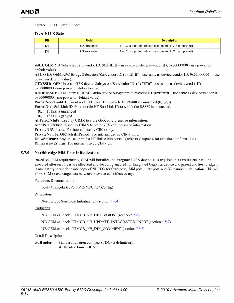
CState: CPU C State support.
SSID: OEM NB Subsystem/Subvendor ID. (0xffffffff – use same as device/vendor ID, 0x00000000 - use power on default value).APCSSID: OEM APC Bridge Subsystem/Subvendor ID. (0xffffffff – use same as device/vendor ID, 0x00000000 - - use power on default value).GFXSSID: OEM Internal GFX device Subsystem/Subvendor ID. (0xffffffff – use same as device/vendor ID, 0x00000000 - use power on default value).AUDIOSSID: OEM Internal HDMI Audio device Subsystem/Subvendor ID. (0xffffffff – use same as device/vendor ID, 0x00000000 - use power on default value).ParentNodeLinkID: Parent node HT Link ID to which the RS880 is connected (0,1,2,3)ParentNodeSubLinkID: Parent node HT Sub Link ID to which the RS880 is connected.
(0,1) If link is unganged (0) If link is ganged.
AllPcieGfxInfo: Used by CIMX to store GFX card presence information. AmdPcieGfxInfo: Used by CIMX to store GFX card presence information. PrivateNBVoltage: For internal use by CIMx only.PrivateNumberOfCyclesInPeriod: For internal use by CIMx only.DhlwSmiPort: Any unused port for HT link width control (refer to Chapter 8 for additional information).DhlwPrivateStatus: For internal use by CIMx only.
5.7.5 Northbridge Mid-Post Initialization
Based on OEM requirements, CIM will initialize the Integrated GFX device. It is required that this interface call be executed after resources are allocated and decoding enabled for Integrated Graphics device and parent and host bridge. It is mandatory to use the same copy of NBCFG for Start post, Mid post , Late post, and S3 resume initialization. This will allow CIM to exchange data between interface calls if necessary.
Functions Documentation:
void (*ImageEntryPointPtr)(NBCFG* Config)
Parameters:
Northbridge Start Post Initialization (section 5.7.4)
Callbacks:
NB OEM callback ”CIMCB_NB_GET_VBIOS” (section 5.8.6)
NB OEM callback ”CIMCB_NB_UPDATE_INTEGRATED_INFO” (section 5.8.7)
NB OEM callback “CIMCB_NB_DDI_COMMEN” (section 5.8.7)
Detail Description:
stdHeader – Standard function call (see STDCFG definition).stdHeader.Func = 0x5.
Table 5-13 CState
Bit Field Description
[2] C2 supported 1 – C2 supported (should also be set if C1E supported)
[3] C3 supported 1 – C3 supported (should also be set if C1E supported)
46143 AMD RS880 ASIC Family BIOS Developer’s Guide 3.00 © 2010 Advanced Micro Devices, Inc.5-14
Interface Definition
5.7.6 Northbridge PCIe Late Post Initialization
The RS880 late post initialization helps enable link ASPM, switch link speed to GEN2 program port capability. It is mandatory to use the same copy of PCIECFG for Late Post and S3 Resume initialization. This will allow the CIM to exchange data between interface calls if necessary.
Functions Documentation:
void (*ImageEntryPointPtr)(PCICFG* Config)
Parameters:
See Northbridge PCIe® Early Initialization (section 5.7.3)
Detail Description:
stdHeader – Standard function call (see STDCFG definition).stdHeader.Func = 0x6.
Note: Only stdHeader needs to be filled out rest of the parameters in PCICFG are not required for this call and should be set to 0.
5.7.7 Northbridge Late Post Initialization
Based on OEM requirements, the CIM will initialize misc. SSID. Also the CIM will help do necessary programming to prepare NB to boot to the OS. It is mandatory to use the same copy of NBCFG for Start Post, Mid Post, Late Post, and S3 Resume initialization. This will allow CIM to exchange data between interface calls if necessary.
Functions Documentation:
void (*ImageEntryPointPtr)(NBCFG* Config)
Parameters:
See Northbridge Start Post Initialization (section 5.7.4)
Detail Description:
stdHeader – Standard function call (see STDCFG definition). stdHeader.Func = 0x5.
5.7.8 Northbridge PCIe® S3 Resume Initialization
The CIM will help do the necessary programming to prepare PCIe® to resume from sleep state. Certain northbridge PCIe Port Configuration registers need to be restored prior to this call (see Resume from S3 State (section 7.1.2)). It is mandatory to use the same copy of PCIECFG for Late Post and S3 Resume initialization. This will allow CIM to exchange data between interface calls if necessary.
Functions Documentation:
void (*ImageEntryPointPtr)(PCICFG* Config)
Parameters:
Detail Description:
stdHeader – Standard function call (see STDCFG definition).stdHeader.Func = 0x7.
See Northbridge PCIe Late Post Initialization (section 5.7.7)
© 2010 Advanced Micro Devices, Inc. 46143 AMD RS880 ASIC Family BIOS Developer’s Guide 3.005-15
Callback Interface Definition
5.7.9 Northbridge S3 Resume Initialization
CIM will help do the necessary programming to prepare NB to resume from sleep state. Certain Northbridge PCI configuration registers needs to be restored prior to this call (see Resume from S3 State (section 7.1.2). It is highly recommended to use same copy NBCFG for Start post, Late post and S3 resume initialization. This will allow CIM to exchange data between interface calls if necessary.
Functions Documentation:
void (*ImageEntryPointPtr)(NBCFG* Config)
Parameters:
See Northbridge Start Post Initialization (section 5.7.4)
Detail Description:
stdHeader – Standard function call (see STDCFG definition).stdHeader.Func = 0x8.
5.7.10 Northbridge Register Restrictions
The Northbridge Bus 0, Device 0, Function 0, registers 0x78 – 0x7B are reserved for internal CIMX use. These registers should not be used by any other application or interface.
5.8 Callback Interface Definition
5.8.1 PCIE OEM Callback “CIMCB_PCIE_SLOT_RESET_DEASSERT”
This callback function dedicated to deassert PCIe slot reset signal (for platforms that use GPIO for slot reset).
Functions Documentation:
UINT32 (*pCallBack)(UINTN Param1, UINTN Param2, PCICFG* pConfig)
Parameters:
Param1: Function identifier 0x102.Param2: Port bit map to deassert reset. BIT2 – Port2, BIT3 – Port3, … etc. For example: Param2 = 0x1c – request deassert reset on Port2/3/4.pConfig: See Northbridge PCIE Early Initialization (section 5.7.3)
Return Values:
CIM_SUCCESS (0x00000000): If platform has dedicated GPIO reset for port and support port reset logic for at least one requested port.CIM_UNSUPPORTED (0x80000001): If platform has does not have GPIO reset for any of requested ports.
5.8.2 PCIE OEM Callback “CIMCB_PCIE_SLOT_RESET_ASSERT”
This callback function dedicated to deassert PCIe® slot reset signal (For platforms that use GPIO for slot reset).
Functions Documentation:
UINT32 (*pCallBack)(UINTN Param1, UINTN Param2, PCICFG* pConfig)
Parameters:
Param1: Function identifier 0x103.Param2: Port bit map to assert reset. BIT2 – Port2, BIT3 – Port3, … etc. For example Param2 = 0x1c – request assert reset on Port2/3/4. pConfig: See Northbridge PCIE Early Initialization (section 5.7.3)
Return Values:
46143 AMD RS880 ASIC Family BIOS Developer’s Guide 3.00 © 2010 Advanced Micro Devices, Inc.5-16
Callback Interface Definition
CIM_SUCCESS (0x00000000): If platform has dedicated GPIO reset for port and support port reset logic for at least one requested port.CIM_UNSUPPORTED (0x80000001): If platform has does not have GPIO reset for any of requested ports.
5.8.3 PCIE OEM Callback “CIMCB_PCIE_SLOT_RESET_SUPPORT”
This callback function dedicated to deassert PCIE slot reset signal (For platforms that use GPIO for slot reset).
Functions Documentation:
UINT32 (*pCallBack)(UINTN Param1, UINTN Param2, PCICFG* pConfig)
Parameters:
Param1: Function identifier 0x104.Param2: Port bit map to test if port has GPIO reset capability. BIT2 – Port2, BIT3 – Port3, … etc. For example Param2 = 0x10 – request assert reset on Port4. pConfig: See Northbridge PCIE Early Initialization (section 5.7.3)
Return Values:
CIM_SUCCESS (0x00000000): If port has GPIO reset capability.CIM_UNSUPPORTED (0x80000001): If port does not have GPIO reset capability.
5.8.4 PCIE OEM Callback ”CIMCB_PCIE_TRAINING_COMPLETE”
This callback function called after port training completed and device detected. This can be used to force to disable a device).
Functions Documentation:
UINT32 (*pCallBack)(UINTN Param1, UINTN Param2, PCICFG* pConfig)
Parameters:
Param1: Function identifier 0x101. Param2: Port number. DEV2 – 0x2, DEV3 – 0x3 …. pConfig: See Northbridge PCIE Early Initialization (section 5.7.3)
Return Values:
CIM_SUCCESS (0x00000000): Keep port enable.CIM_DISABLEPORT (0x80000002): Force port disable/hide/poweroff.
5.8.5 NB OEM Callback ”CIMCB_NB_UMA_STATE”
This callback function is called after the UMA configuration is validated. This call can be used to save UMA state (for example, in NVS). For instance, it can be used on following boot to determine CPU correct setting for CpuBufferOptimization (see Northbridge HT Initialization (section 5.7.2)).
Functions Documentation:
UINT32 (*pCallBack)(UINT32 Param1, UINT32 Param2, PCICFG* pConfig)
Parameters:
Param1: Function identifier 0x201. Param2: 0=PCI reset not required. 1=PCI reset required. pConfig: See Northbridge Start Post Initialization (section 5.7.4)
Return Values:
CIM_SUCCESS (0x00000000).
© 2010 Advanced Micro Devices, Inc. 46143 AMD RS880 ASIC Family BIOS Developer’s Guide 3.005-17
Callback Interface Definition
5.8.6 NB OEM Callback ”CIMCB_NB_GET_VBIOS”
This callback function called after to get image of option ROM for integrated GFX for Surround View initialization. It is required to execute the special VBIOS post prior to returning the pointer to the VBIOS image on mobile platforms. The special VBIOS post can be executed by calling offset 64H of the VBIOS with ax = 128h.
Functions Documentation:
UINT32 (*pCallBack)(UINTN Param1, void** Param2, PCICFG* pConfig)
Parameters:
Param1: Function identifier 0x202. Param2: Pointer on pointer to which needs to be initialized physical address location of uncompressed VBIOS image.pConfig: See Northbridge Start Post Initialization (section 5.7.4)
Return Values:
CIM_SUCCESS (0x00000000).
5.8.7 NB OEM Callback ”CIMCB_NB_UPDATE_INTEGRATED_INFO”
This callback function called after to get image of option ROM for integrated GFX for Surround View initialization.
Functions Documentation:
UINT32 (*pCallBack)(UINTN Param1, ATOM_INTEGRATED_SYSTEM_INFO_V2* Param2, PCICFG* pConfig)
Parameters:
Param1: Function identifier 0x203. Param2: Pointer to ATOM_INTEGRATED_SYSTEM_INFO_V2 (see CIMRS880.INC for the ATOM_INTEGRATED_SYSTEM_INFO_V2 definition)pConfig: See Northbridge Start Post Initialization (section 5.7.4)
Return Values
CIM_SUCCESS (0x00000000).
5.8.8 NB OEM Callback “CIMCB_NB_DDI_COMMEN”
This callback function called to sert state of COMM_EN signal for ADD2 card detection.
Functions Documentation:
UINT32 (*pCallBack)(UINTN Param1, UINTN Param2, NBCFG* pConfig)
Parameters:
Param1: Function identifier 0x205.Param2: 1/0 - Assert/Deassert COMM_EN signalpConfig: See Northbridge Start Post Initialization (section 5.7.4)
Return Values:
CIM_SUCCESS (0x00000000).
46143 AMD RS880 ASIC Family BIOS Developer’s Guide 3.00 © 2010 Advanced Micro Devices, Inc.5-18
Integrated Info Table
5.9 Integrated Info Table
5.9.1 Overview
The integrated Info Table (ATOM_INTEGRATED_SYSTEM_INFO_V2) is used to help communicate platform requirements to the VBIOS/GFX driver. In most instances the CIM will automatically fill the integrated Info Table. However, some parameters needs to be directly adjusted based on platform requirements (see section 5.8.7). The integrated Info Table is defined in CIMRS880.INC.
5.9.2 Voltage Control
To enable PWM voltage control usNumberOfCyclesInPeriod/usMaxNBVoltage/usMinNBVoltage/usBootUpNBVoltage parameters needs to be filled up. Note that the value for this parameters depend on platform implementation PWM voltage control logic. Also note that the CIMX will request the driver to stay at max voltage at all times if PCIE Gen2 capability is enabled for any port.
The following is an example for typical dual voltage level control (1.0V – 1.1V) implementation:
• usNumberOfCyclesInPeriod = 0x8019
• usMaxNBVoltage =0x1A
• usMinNBVoltage = 0x00
• usBootUpNBVoltage = 0x1A
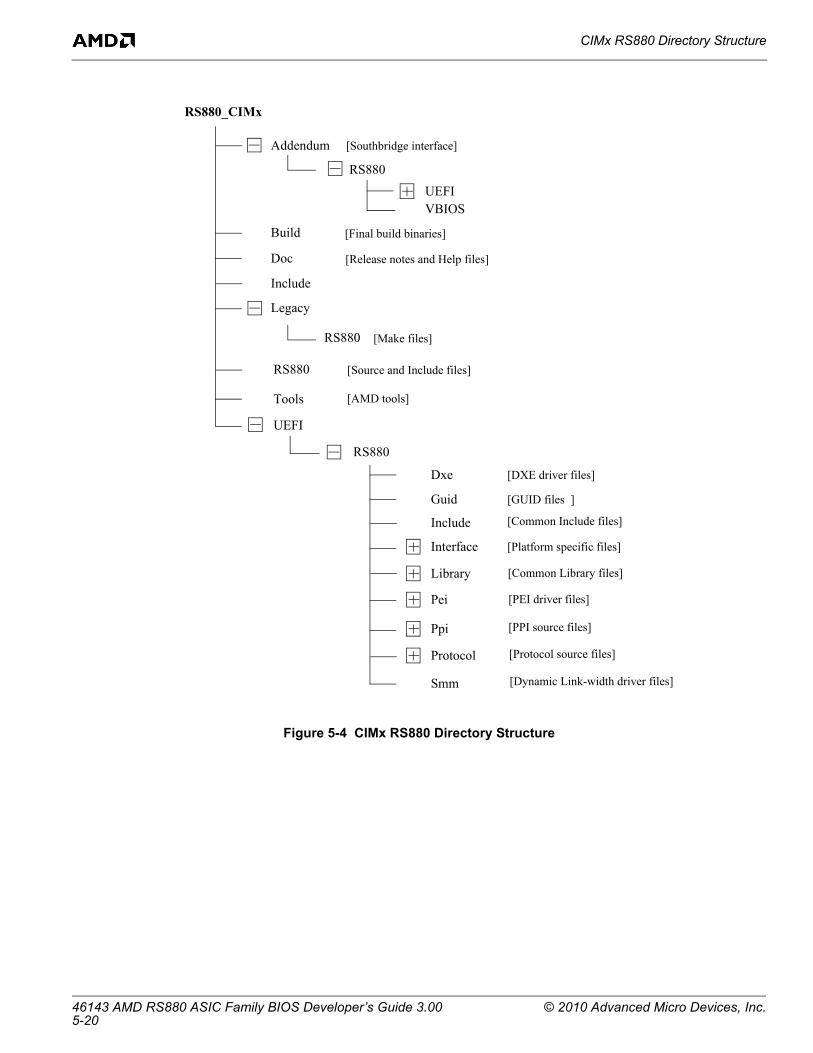
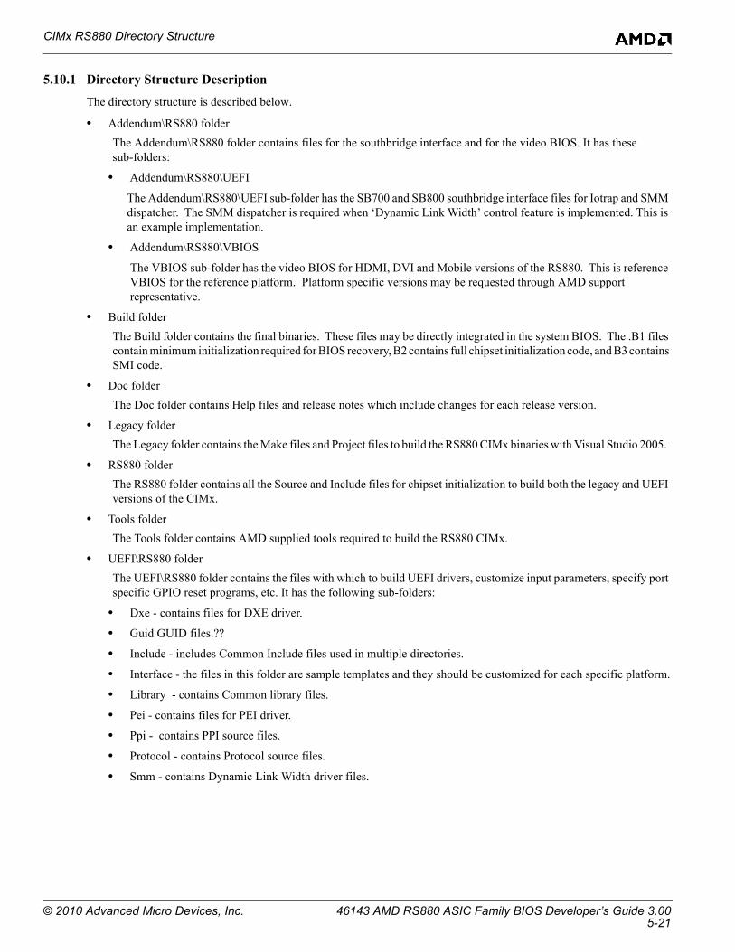
5.10 CIMx RS880 Directory Structure
The RS880 CIMx files are organized in different folders for ease of maintenance and integration. There are two versions of RS880 CIMx - Legacy and UEFI. The structure is similar for both versions but some files may be different or unique for a given version. In addition to the Legacy and UEFI folders, there are other folders including the Addendum, Buid, Doc, etc folders. The figure below illustrates the RS880_CIMx directory structure.
© 2010 Advanced Micro Devices, Inc. 46143 AMD RS880 ASIC Family BIOS Developer’s Guide 3.005-19
CIMx RS880 Directory Structure
Figure 5-4 CIMx RS880 Directory Structure
RS880_CIMx
Build
Addendum
Doc
Include
Legacy
RS880
RS880
Tools
UEFI
RS880
[Southbridge interface]
[Final build binaries]
[Release notes and Help files]
[Make files]
[Source and Include files]
[AMD tools]
Guid
Include
Interface
Library
Pei
Ppi
Protocol
Smm
[GUID files ]
[Common Include files]
[Platform specific files]
[Common Library files]
[PEI driver files]
[PPI source files]
[Protocol source files]
[Dynamic Link-width driver files]
RS880
Dxe [DXE driver files]
UEFIVBIOS
46143 AMD RS880 ASIC Family BIOS Developer’s Guide 3.00 © 2010 Advanced Micro Devices, Inc.5-20
CIMx RS880 Directory Structure
5.10.1 Directory Structure Description
The directory structure is described below.
• Addendum\RS880 folder
The Addendum\RS880 folder contains files for the southbridge interface and for the video BIOS. It has these sub-folders:
• Addendum\RS880\UEFI
The Addendum\RS880\UEFI sub-folder has the SB700 and SB800 southbridge interface files for Iotrap and SMM dispatcher. The SMM dispatcher is required when ‘Dynamic Link Width’ control feature is implemented. This is an example implementation.
• Addendum\RS880\VBIOS
The VBIOS sub-folder has the video BIOS for HDMI, DVI and Mobile versions of the RS880. This is reference VBIOS for the reference platform. Platform specific versions may be requested through AMD support representative.
• Build folder
The Build folder contains the final binaries. These files may be directly integrated in the system BIOS. The .B1 files contain minimum initialization required for BIOS recovery, B2 contains full chipset initialization code, and B3 contains SMI code.
• Doc folder
The Doc folder contains Help files and release notes which include changes for each release version.
• Legacy folder
The Legacy folder contains the Make files and Project files to build the RS880 CIMx binaries with Visual Studio 2005.
• RS880 folder
The RS880 folder contains all the Source and Include files for chipset initialization to build both the legacy and UEFI versions of the CIMx.
• Tools folder
The Tools folder contains AMD supplied tools required to build the RS880 CIMx.
• UEFI\RS880 folder
The UEFI\RS880 folder contains the files with which to build UEFI drivers, customize input parameters, specify port specific GPIO reset programs, etc. It has the following sub-folders:
• Dxe - contains files for DXE driver.
• Guid GUID files.??
• Include - includes Common Include files used in multiple directories.
• Interface - the files in this folder are sample templates and they should be customized for each specific platform.
• Library - contains Common library files.
• Pei - contains files for PEI driver.
• Ppi - contains PPI source files.
• Protocol - contains Protocol source files.
• Smm - contains Dynamic Link Width driver files.
© 2010 Advanced Micro Devices, Inc. 46143 AMD RS880 ASIC Family BIOS Developer’s Guide 3.005-21

CIMx RS880 Directory Structure
46143 AMD RS880 ASIC Family BIOS Developer’s Guide 3.00 © 2010 Advanced Micro Devices, Inc.5-22
Chapter 6SurroundViewTM Feature
6.1 SurroundViewTM Feature (Dual Display)
SurroundViewTM is the technology that helps provide support of multiple traditional CRT monitors and flat panel displays by turning on both internal graphics and external PCIe® graphics devices under the operating system. When the SurroundView feature is enabled, the SBIOS sets the internal graphics as the secondary display device, while keeping the external PCIe graphics device as the primary display device. Note that the primary graphics device should be an AMD PCIe graphics card.
Note: To enable CIMX Surroundview support see Northbridge Start Post Initialization (section 5.7.4), and NB OEM call back ”CIMCB_NB_GET_VBIOS” (section 5.8.6).
© 2010 Advanced Micro Devices, Inc. 46143 AMD RS880 ASIC Family BIOS Developer’s Guide 3.006-1

SurroundViewTM Feature (Dual Display)
This page is left blank intentionally.
46143 AMD RS880 ASIC Family BIOS Developer’s Guide 3.00 © 2010 Advanced Micro Devices, Inc.6-2

Chapter 7Power Management
7.1 Sx State Power Management
During certain Sx states (such as S1) the system maintains power to the RS880 and all register settings are retained. Therefore, no action is required when the system resumes. However, under other S states (such as S3) typical designs will shut down power to the RS880 and all of the register settings will be lost.
The SBIOS is responsible for reinitializing all of the RS880 registers. Reinitializing the RS880 registers after S3 can be done by either restoring the tables of register settings which were saved to non-volatile storage prior to entering S3, or by initializing all registers as if from cold.
For most configurations restoration by table is not practical. The recommendation is to re-execute the initialization code.
The remaining NB registers are covered in section 7.1.1.
7.1.1 Register Restoration
The registers listed in this section are restored after the system memory is made available by bringing the system RAM out of self refresh mode.
On RS880 designs the main system memory is controlled by the memory controller in the AMD CPU. (For more information on saving and restoring the memory controller settings, along with entering and exiting self refresh mode, refer to the “AMD Kernel BIOS writers guide”).The reference BIOS saves the registers listed in this section prior to entering S3. It then restores them after system memory is available on resume from S3.
Note: The list of registers in the following sections is subject to change. If an OEM customer changes any other registers in the RS880 during POST, then they must also be restored on an S3 resume.
• Integrated Graphics Device (1:5:0)
• 0x10 - 0x13
• 0x14 - 0x17
• 0x18 - 0x1B
• 0x24 - 0x27
• 0x04 - 0x06
• APC Bridge (0:1:0)
• 0x18 - 0x1B
• 0x20 - 0x23
• 0x24 - 0x27
• 0x2C - 0x2f
• 0x04 - 0x06
• Northbridge (0:0:0)
• 0x04 - 0x06
• 0x4C - 0x4f
• 0x8C - 0x8f
• PCIE Bridges (0:2/3/4/5/7/9/10:0)
• 0x18 - 0x1B
• 0x20 - 0x23
© 2010 Advanced Micro Devices, Inc. 46143 AMD RS880 ASIC Family BIOS Developer’s Guide 3.007-1
S3 PCIe® Graphics BAR Save/Restore Issue Workaround
• 0x24 - 0x27
• 0x2C - 0x2f
• 0x04 - 0x06
7.1.2 Resume from S3 State
When the system wakes up from S3 the BIOS is initially executed from ROM, once it is determined this is an S3 resume. The SBIOS is responsible for restoring the system memory controller’s configuration as outlined in the “AMD Kernel BIOS Writer’s Guide”.
Once the system memory is available, BIOS should then restore the RS880 registers that were saved prior to entering S3.
Note: Platform BIOS should read SB strapping to determine if it is in internal clock mode. If yes, it must set clkconfig: 0xE4[1]. This needs to be done on normal POST as well as on S3 Resume.
7.2 S3 PCIe® Graphics BAR Save/Restore Issue Workaround
Below is the full detail and requirements for the workaround documented in the product advisory PA_RSx80Q2.
(“RV6xx/M8x and RS780/RS880 Black Screen Hang During S3 Testing”).
7.2.1 BAR Restoration Process and Architecture
1 The BAR registers will only be guaranteed to be restored after the System BIOS CIMx code has completed with the PCIe link training sequences. In addition, the command registers cannot be restored to the correct value because the operating system will set those registers to value 0 prior to S3.
2 Since the operating system has the ability to re-allocate the BAR windows of PCIe® bridges, and because any general purpose port (GPP) or graphics core root complex bridge may support one or more graphics devices including hot-plug support, the complete BIOS solution must scan for and be aware of the graphics devices that are available behind any of the available PCIe bridges (not just bus 0, device 2, function 0). Code must save/restore BARs for any PCIe bridge device that could possibly support graphics and detect any graphics device (by scanning for and testing the class code of that device) behind the bridge.
3 For designs in which different configurations can be productized or in which hybrid graphics can be disabled, the bus/device/function address of the end point device may change due to the hiding of the other resources or unused devices. Some designs may also implement hardware (e.g., PCIe switches) which would alter the location of the end point device. Therefore, the SBIOS must scan for the location of the graphics device behind any bridge rather than assuming it will always be at the same location.
7.2.2 Post Time
• BIOS kernel programs BAR registers. Nothing to save/restore related to S4 or reboot.
• RAM and device registers are cleared on every reboot or S4 and the BIOS is re-posted.
• Use the RS880 host device NBMisc register 0x0C to get the bit map of hidden PCie ports to avoidsaving registers for those bridges or devices. Save this map.
• In late post, after the CIMx wrapper code functions were already called, the SBIOS must scan the subordinate bus numbers for the graphics devices, check that the link status register 0xA5 value is greater than or equal to 0x10, and verify that the class code matches that for a graphics device as defined by the PCI specification. The BIOS should not assume that these devices are at specific addresses (bus/device/function) since PCIe endpoint addresses will move around depending on hardware and feature configuration settings.
• Save a corresponding map in System Management mode (SMM) memory of the bus/dev/func of each graphics devices behind each bridge (port) that is found during post time. Do not include hot plug ports in this scan or map since, in the hot plug case, the correct BIOS implementation will result in the operating system calling a different code path (Windows Vista® multi-level resource rebalancing triggered by ACPI BIOS _DSM method) to restore endpoint registers on S3 resume that will always consistently work as long as the bridge BAR registers are configured as expected. For a detailed explanation on how Microsoft Windows Operating Systems handle the PCI and PCIe BAR resources, reference the Microsoft® white-paper at
46143 AMD RS880 ASIC Family BIOS Developer’s Guide 3.00 © 2010 Advanced Micro Devices, Inc.7-2
S3 PCIe® Graphics BAR Save/Restore Issue Workaround
http://www.microsoft.com/whdc/system/bus/pci/resources.mspx.
• When the operating system is initializing ACPI in late post, it makes a call to the BIOS and the BIOS is required to save the pcicfg Command Register for all un-hidden PCIe root complex bridges.
• When the operating system is initializing ACPI, it makes a call to the BIOS and the BIOS is required to save the pcicfg Command Register for all non-hot plug PCIe endpoint graphics devices.
• The BIOS is required to configure an I/O-based System Management Interrupt-trap of the SLP_TYP register as explained in the SB700 Register Programming Requirements documentation. The Sleep trap will trigger on any Sleep state transition. The SMI handler must disable the trap once it is triggered and BIOS ASL code must only set the SLP2SMI enable bit for that trap when the PTS method for the desired Sleep State is called by the operating system.
7.2.3 When Entering S3
• The BIOS is required to help enable the I/O trap of the SLP_TYP register (as explained in the SB700 Register Programming Requirements document) by writing to the SLP2SMI enable register in the _PTS ACPI method for S3 sleep state.
• When the operating system writes the SLP_TYP register, it will be enabled to trigger an SMI. SBIOS must have implemented a handler that calls a specific function for the S3 sleep case. The main sleep2smi handler (already implemented in Phoenix BIOS MISER code) should direct the calls for the S0-S3 transition to the associated correct sleep type handler routines. This functionality is normally already supplied by the BIOS vendor code for AMD chipsets, and the ODM should only implement a subordinate helper routine for the S0-S3 state. For example, in Phoenix BIOS, these routines are called REGISTER_ACPI_FN SLEEP_TRAP32 functions.
• The SBIOS saves the 32-bit command register offset 0x04 (in the same place that was done previously during POST) for the bridge, but ignores the lower byte of the register read back at this time (the operating system will have sometimes set it to 0) and only saves the upper 3 bytes in the DWORD location in memory. The data for the lower byte of that register that was previously saved during post time is not altered.
• The SBIOS uses the previously saved maps to scan for and save the PCIe Bridge BARs (registers as defined for PCICFG Type 1 header) in a table in memory. It also checks behind the bridge for any graphics device as per the previously determined PFAs (bus/dev/func) expected in that slot (port).
• If there is a graphics device behind the bridge, then the PCICFG Type 0 BAR register locations need to be saved in their own unique table (one for each possible graphics device behind each possible bridge).
• If any registers read back 0xFFFF then the expected device was powered down and the registers should NOT be saved.
7.2.4 When Resuming from S3
PCIe® Root Complex bridges are restored by CIMx code such that any PCIe links with PCIe endpoint devices behind the bridges must be “re-trained” prior to any access to either the bridge BAR or endpoint BAR registers. The sequence of suggested code calls in the S3 resume path must occur as follows:
1 InitPcieAtEarly
a Call CIMx function NB_INIT_PCIE_EARLY (Medium priority)
2 RestoreRS880S3Config (Low priority, this must happen only after the CIMx PCIE_EARLY call)
a RestoreNBConfig (restore registers for RS880 host (bus0, dev0, func0))
b RestoreAGPConfig (restore registers for IGP bridge (if powered))
c RestorePCIEBridgeConfig (restore registers for S3 PCIe BAR workaround here)
d RestoreOtherPCIConfig (restore registers for any special on-board fixed PCI (not PCIe) devices)
e oemCustomRestorePcieDevices (restore registers for any special on-board PCIe devices)
3 InitNbS3ResumeFar (Lowest priority, this must happen only after the RestoreRS880S3Config)
a Call CIMx function NB_INIT_PCIE_S3
b Call CIMx function NB_INIT_NB_S3
© 2010 Advanced Micro Devices, Inc. 46143 AMD RS880 ASIC Family BIOS Developer’s Guide 3.007-3

S3 PCIe® Graphics BAR Save/Restore Issue Workaround
The S3 Resume Time PCIe BAR workaround register restore is implemented in item 2c) which corresponds to the functionality of RestoreRS880S3Config RestorePCIEBridgeConfig as follows:
• Get the hidden bridge bits from NBMisc REG0x0C. The bits that are clear indicate active PCIe bridges for which the BARs must be restored with corresponding data that was previously saved during the S3 sleep trap time.
• Test BIT2. If BIT2 is set (port is disabled/hidden) then skip to test the next port (BIT3).
• A generic common register restore routine is suggested. This routine should not attempt to restore any registers for a specified PCIe device or bridge address if the Vendor/Device ID register (offset 0x00 in the PCI Configuration space) reads back 0xFFFFFFFF) which indicates that the device or bridge is not present.
• If BIT2 = 0, then restore the 32-bit registers for PCI address 80001000h (Bus0, Dev2, Func 0) in this order: offset 0x18, 0x1c, 0x20, 0x24, 0x2Ch, 0x30, 0x3Ch, 0x04. These registers correspond to the PCI specification definition for the Type 1 PCI Configuration space header (used for PCI-to-PCI Bridges corresponding to each PCIe root complex port).
• After restoring the PCIe root complex bridge registers for a particular port, check the previously stored (from post time) bit map and table of the end-point device PCI addresses (bus/device/function number) to determine if there is expected to be a graphics device behind this bridge.
• If there was a corresponding post time graphics device PFA previously saved for the expected device behind this port, then proceed to restore the previously saved 32-bit BAR and Command registers for that PCI device address. The registers must be restored in this order: offset 0x10, 0x14, 0x18, 0x1C, 0x20, 0x24, 0x04. These registers correspond to the PCI specification definition from the Type 0 PCI Configuration space header (used for PCIe endpoint devices).
• The corresponding PCI address for each of the RS880 root complex bridge ports is as follows:
nbmisccfg 0x0C BIT2 = 0, the PCI address is 8001000h (Bus 0 Dev 2 Fn 0).
nbmisccfg 0x0C BIT3 = 0, the PCI address is 8001800h (Bus 0 Dev 3 Fn 0).
nbmisccfg 0x0C BIT4 = 0, the PCI address is 8002000h (Bus 0 Dev 4 Fn 0).
nbmisccfg 0x0C BIT5 = 0, the PCI address is 8002800h (Bus 0 Dev 5 Fn 0).
nbmisccfg 0x0C BIT6 = 0, the PCI address is 8003000h (Bus 0 Dev 6 Fn 0).
nbmisccfg 0x0C BIT7 = 0, the PCI address is 8003800h (Bus 0 Dev 7 Fn 0).
nbmisccfg 0x0C BIT9 = 0, the PCI address is 8004800h (Bus 0 Dev 9 Fn 0).
nbmisccfg 0x0C BIT10 = 0, the PCI address is 8005000h (Bus 0 Dev 0x0A Fn 0).
• Repeat the steps for all of the remaining root complex bridge ports BITn (if set then go to Test next port BITn+1) where n = 3, 4, 5, 6, 7, 9, 10. Note that port 8 is reserved (used for Northbridge-Southbridge communication) and should not have any associated code to save or restore registers.
46143 AMD RS880 ASIC Family BIOS Developer’s Guide 3.00 © 2010 Advanced Micro Devices, Inc.7-4
Chapter 8Dynamic HyperTransportTM Link Width
This chapter provides detail implementation of HT (HyperTranspotTM) Link Width Control in BIOS. The important features are:
• Expanded NBCFG structure to include:
• Dynamic Link Width configuration input parameters.
• SMI port number. Any unused port can be used.
• Dynamic Link Width private status. This is used only by SMI routine; no user interface is needed.
• Dynamic Link Width SMI Handler
8.1 CIMx Support
CIMx-RS880 provides an interface in the form of a call to service SMI requests referenced as CIMx SMI Handler.
8.2 Expanded NBCFG Structure
Input configuration parameter structure is expanded to provide additional configuration options for the HT Link Width Control feature.
typedef struct _NBCFG{
STDCFG stdHeader;
union {
PLACEHOLDER PlaceHolder;void* DebugPtr;
}DEBUGPTR;
UINT32 Status;
NBBITCFG nbConfiguration;
GFXBITCFG gfxConfiguration;
SPBITCFG spConfiguration;
UINT16 UMABase;
UINT16 UMASize;
UINT16 SysMemTomLo;
UINT16 SysMemTomHi;
UINT16 MCLK;
UINT16 ECLK;
union {
PLACEHOLDER PlaceHolder;SPTBLHEADER* spOemInitTablePtr;
}OEMINITTBL;
UINT8 CState;
UINT32 SSID;
UINT32 APCSSID;
UINT32 GFXSSID;
UINT32 AUDIOSSID;
UINT8 ParentNodeLinkID;
UINT8 ParentNodeSubLinkID;
UINT16 AllPcieGfxInfo;
UINT16 AmdPcieGfxInfo;
UINT16 PrivateNBVoltage;
UINT16 PrivateNumberOfCyclesInPeriod;
HTLWBITCFG DhlwConfiguration;
© 2010 Advanced Micro Devices, Inc. 46143 AMD RS880 ASIC Family BIOS Developer’s Guide 3.008-1
CIMx Dynamic Link Width SMI Handler
UINT16 DhlwSmiPort;
UINT16 DhlwPrivateStatus;
UINT64 Reserved3;
}NBCFG;
typedef struct {
UINT32 DhlwEnabled :2; // CPU-NB HT Width Control
// 0 Auto – Recommended selection for the board
// 1 Disable – firmware is not installed
// 2 Enable – firmware is installed
UINT32 DhlwPStateControl :2; // CPU-NB Pstate support.
// 0 Auto – Recommended selection for the board
// 1 Disable – P-State control disabled in SMI
// 2 Enable – P-State control enabled in SMI
UINT32 Reserved :3; // Reserved
UINT32 DhlwHtT0TimeOverride :2; // ToTime override
// 0 Auto – recommended selection for the board
// 1 Disable – Do not override T0Time
// 2 Enable – Override T0Time.
}HTLWBITCFG;
8.3 CIMx Dynamic Link Width SMI Handler
CIMx provides an interface call (NbDynamicLinkWidthSmiHandler) to service Dynamic Link Width SMI requests. This interface call is located in the “B3” binary image. To minimise latency, the “B3” image must be copied to the system memory (SMRAM) prior to its usage.
Functions Documentation:
void (*ImageEntryPointPtr)(NBCFG* Config)
Parameters:
SMI handler can use the same instance or a copy of NBCFG used by Northbridge Start/MID/Late Post Initialization. The function for Dynamic Link Width SMI Handler is NB_DHLW_SMI_HANDLER 0x11)
Callbacks:
None
8.3.1 Dynamic Link Width SMI Requests
The functionality to transition HT link width resides in the CIMx Dynamic Link Width SMI Handler. The HT Link Width Controller component in the RS880 will use a write to the I/O port specified in NBCFG.DhlwSmiPort. SBIOS should provide the functionality to set up for SMI generation, enable/detect/clear SMI source/status.
The recommended method to generate an SMI is:
• Select an unused I/O port for the system.
• Set the selected 12-bit I/O port address (bits [15:4]) and a 4-bit mask in one of the 4 unused ProgramIoRange registers. For SB700/SB800 they are at PMIO 0xA0 through 0xA7
• Clear the status bit for this range in PMIO register 0xA9.
• Enable the I/O monitoring for this range in PMIO register 0xA9
Note: Currently the use of software SMI is not recommended to avoid interoperability problems with software C1E implementation.
46143 AMD RS880 ASIC Family BIOS Developer’s Guide 3.00 © 2010 Advanced Micro Devices, Inc.8-2

Northbridge Register Restrictions
8.4 Northbridge Register Restrictions
The Northbridge Bus 0, Device 0, Function 0, registers 0x78 – 0x7B are reserved for internal CIMX use. These registers should not be used by any other application or interface.
© 2010 Advanced Micro Devices, Inc. 46143 AMD RS880 ASIC Family BIOS Developer’s Guide 3.008-3

Northbridge Register Restrictions
This page is left blank intentionally.
46143 AMD RS880 ASIC Family BIOS Developer’s Guide 3.00 © 2010 Advanced Micro Devices, Inc.8-4
Appendix ARevision History
Rev 3.00 (Oct 2010)
• PDF: 46143_rs880_bdg_pub_3.00. (This version is for public release)• General edits.• Removed section 5.10 Example (Northbridge HT Initialization).
Rev 1.06 (April 2010)
• PDF: 46143_rs880_bdg_nda_1.06.• Added variant RS785E to the document..• Added new section 5.10, “ CIMx RS880 Directory Structure”, on page 5-19.
Rev 1.05 (November 2009)
• PDF: 46143_rs880_bdg_nda_1.05.• Removed variant RS880C from the document.• Added a note to section 7.1.2, “Resume from S3 State‚’ on page 7- 2 on the need to set the clkconfig:0xE4 register.
Rev 1.04 (October 2009)
• PDF: 46143_rs880_bdg_nda_1.04.• Added variant RS880P to the document.
Rev 1.03 (June 2009)
• PDF: 46143_rs880_bdg_nda_1.03.• Updated Table 5-10, “gfxConfiguration,” on page 5-11.
Rev 1.02 (April 2009)
• PDF: 46143_rs880_bdg_nda_1.02.• In section 7.2, “S3 PCIe® Graphics BAR Save/Restore Issue Workaround‚’ on page 7- 2, modified Product Advisory
(PA) title.
Rev 1.01 (March 2009)
• PDF: 46143_rs880_bdg_nda_1.01.• Added section 5.7.10, “Northbridge Register Restrictions‚’ on page 5- 16.• Added section 8.4, “Northbridge Register Restrictions‚’ on page 7- 3.
Rev 1.00 (Jan 2009)
• PDF: 46143_rs880_bdg_nda_1.00.• Preliminary OEM release.
© 2010 Advanced Micro Devices, Inc. 46143 AMD RS880 ASIC Family BIOS Developer’s Guide 3.00A-1

This page intentionally left blank.
46143 AMD RS880 ASIC Family BIOS Developer’s Guide 3.00 © 2010 Advanced Micro Devices, Inc.A-2


![WisDOT Bridge Manual Chapter 36 – Box Culvertson.dot.wi.gov/dtid_bos/extranet/structures/LRFD/BridgeManual/Ch-36.… · LRFD [5.7.1] 36.2.2 Bridge or Culvert Occasionally, the waterway](https://img.pdfslide.us/doc/110x75/5a78b28c7f8b9a21538c127b/wisdot-bridge-manual-chapter-36-box-lrfd-571-3622-bridge-or-culvert.jpg)