Embed Size (px)
Citation preview
AMBA® DDR, LPDDR, and SDRDynamic Memory Controller
DMC-340Revision: r4p0
Technical Reference Manual
Copyright © 2004-2007, 2009 ARM Limited. All rights reserved.ARM DDI 0331G (ID111809)
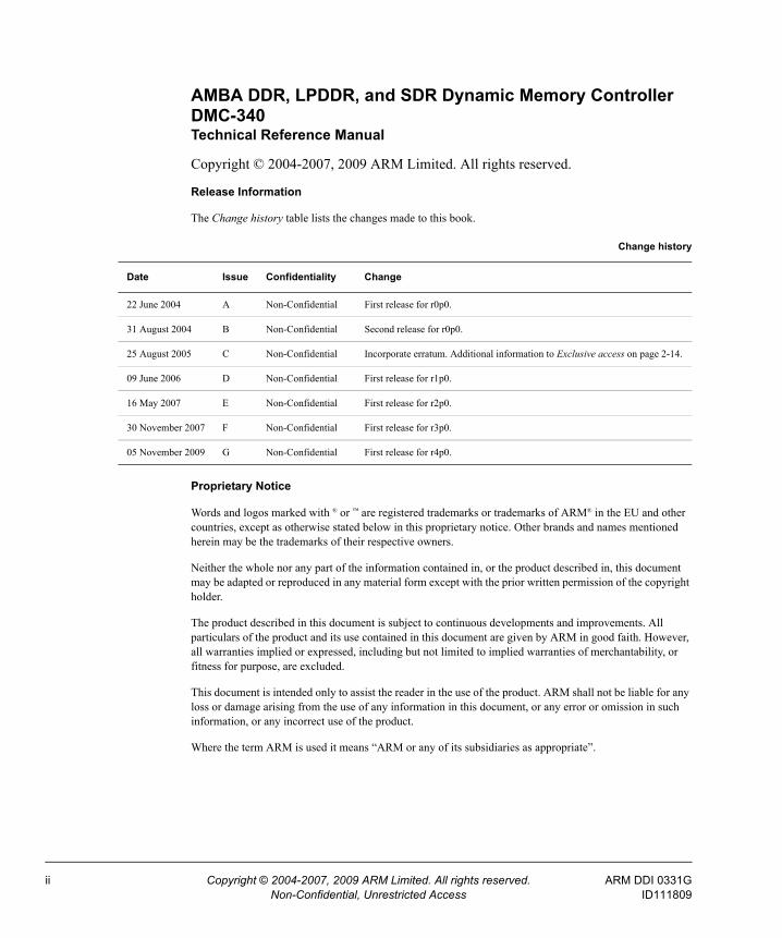
AMBA DDR, LPDDR, and SDR Dynamic Memory Controller DMC-340 Technical Reference Manual
Copyright © 2004-2007, 2009 ARM Limited. All rights reserved.
Release Information
The Change history table lists the changes made to this book.
Proprietary Notice
Words and logos marked with ® or ™ are registered trademarks or trademarks of ARM® in the EU and other countries, except as otherwise stated below in this proprietary notice. Other brands and names mentioned herein may be the trademarks of their respective owners.
Neither the whole nor any part of the information contained in, or the product described in, this document may be adapted or reproduced in any material form except with the prior written permission of the copyright holder.
The product described in this document is subject to continuous developments and improvements. All particulars of the product and its use contained in this document are given by ARM in good faith. However, all warranties implied or expressed, including but not limited to implied warranties of merchantability, or fitness for purpose, are excluded.
This document is intended only to assist the reader in the use of the product. ARM shall not be liable for any loss or damage arising from the use of any information in this document, or any error or omission in such information, or any incorrect use of the product.
Where the term ARM is used it means “ARM or any of its subsidiaries as appropriate”.
Change history
Date Issue Confidentiality Change
22 June 2004 A Non-Confidential First release for r0p0.
31 August 2004 B Non-Confidential Second release for r0p0.
25 August 2005 C Non-Confidential Incorporate erratum. Additional information to Exclusive access on page 2-14.
09 June 2006 D Non-Confidential First release for r1p0.
16 May 2007 E Non-Confidential First release for r2p0.
30 November 2007 F Non-Confidential First release for r3p0.
05 November 2009 G Non-Confidential First release for r4p0.
ii Copyright © 2004-2007, 2009 ARM Limited. All rights reserved. ARM DDI 0331GNon-Confidential, Unrestricted Access ID111809
Confidentiality Status
This document is Non-Confidential. The right to use, copy and disclose this document may be subject to license restrictions in accordance with the terms of the agreement entered into by ARM and the party that ARM delivered this document to.
Unrestricted Access is an ARM internal classification.
Product Status
The information in this document is final, that is for a developed product.
Web Address
http://www.arm.com
ARM DDI 0331G Copyright © 2004-2007, 2009 ARM Limited. All rights reserved. iiiID111809 Non-Confidential, Unrestricted Access

iv Copyright © 2004-2007, 2009 ARM Limited. All rights reserved. ARM DDI 0331GNon-Confidential, Unrestricted Access ID111809
ContentsAMBA DDR, LPDDR, and SDR Dynamic Memory Controller DMC-340 Technical Reference Manual
PrefaceAbout this book ............................................................................................ xviFeedback ...................................................................................................... xx
Chapter 1 Introduction1.1 About the DMC ........................................................................................... 1-21.2 Product revisions ........................................................................................ 1-6
Chapter 2 Functional Description2.1 Functional overview .................................................................................... 2-22.2 Functional operation ................................................................................. 2-10
Chapter 3 Programmers Model3.1 About the programmers model .................................................................... 3-23.2 Register summary ....................................................................................... 3-63.3 Register descriptions .................................................................................. 3-9
ARM DDI 0331G Copyright © 2004-2007, 2009 ARM Limited. All rights reserved. vID111809 Non-Confidential, Unrestricted Access
Contents
Chapter 4 Programmers Model for Test4.1 Integration test registers ............................................................................. 4-2
Chapter 5 Device Driver5.1 Sample device driver .................................................................................. 5-2
Appendix A Signal DescriptionsA.1 Clock and reset signals .............................................................................. A-2A.2 Miscellaneous signals ................................................................................. A-3A.3 AXI signals .................................................................................................. A-6A.4 APB signals .............................................................................................. A-10A.5 Pad interface signals ................................................................................ A-11A.6 EBI signals ................................................................................................ A-14
Appendix B Revisions
Glossary
vi Copyright © 2004-2007, 2009 ARM Limited. All rights reserved. ARM DDI 0331GNon-Confidential, Unrestricted Access ID111809
List of TablesAMBA DDR, LPDDR, and SDR Dynamic Memory Controller DMC-340 Technical Reference Manual
Change history .............................................................................................................. iiTable 1-1 Supported memory device types for different DMC configurations ........................... 1-5Table 2-1 AXI slave interface attributes .................................................................................. 2-12Table 2-2 Address comparison steps example ....................................................................... 2-15Table 2-3 Controller initialization example .............................................................................. 2-35Table 2-4 LPDDR device initialization example ...................................................................... 2-36Table 2-5 Valid system states for the FSMs ............................................................................ 2-38Table 2-6 Recommended power states .................................................................................. 2-39Table 2-7 Dynamic low-power modes operation ..................................................................... 2-43Table 3-1 DMC register summary ............................................................................................. 3-6Table 3-2 memc_status Register bit assignments .................................................................. 3-10Table 3-3 Memory banks chip configuration ........................................................................... 3-11Table 3-4 memc_cmd Register bit assignments ..................................................................... 3-12Table 3-5 direct_cmd Register bit assignments ...................................................................... 3-14Table 3-6 Memory command encoding ................................................................................... 3-14Table 3-7 memory_cfg Register bit assignments .................................................................... 3-16Table 3-8 refresh_prd Register bit assignments ..................................................................... 3-19Table 3-9 cas_latency Register bit assignments ..................................................................... 3-20Table 3-10 t_dqss Register bit assignments ............................................................................. 3-21
ARM DDI 0331G Copyright © 2004-2007, 2009 ARM Limited. All rights reserved. viiID111809 Non-Confidential, Unrestricted Access
List of Tables
Table 3-11 t_mrd Register bit assignments .............................................................................. 3-22Table 3-12 t_ras Register bit assignments ............................................................................... 3-22Table 3-13 t_rc Register bit assignments ................................................................................. 3-23Table 3-14 t_rcd Register bit assignments ............................................................................... 3-24Table 3-15 t_rfc Register bit assignments ................................................................................ 3-25Table 3-16 t_rp Register bit assignments ................................................................................. 3-26Table 3-17 t_rrd Register bit assignments ................................................................................ 3-26Table 3-18 t_wr Register bit assignments ................................................................................. 3-27Table 3-19 t_wtr Register bit assignments ................................................................................ 3-28Table 3-20 t_xp Register bit assignments ................................................................................. 3-29Table 3-21 t_xsr Register bit assignments ................................................................................ 3-29Table 3-22 t_esr Register bit assignments ............................................................................... 3-30Table 3-23 memory_cfg2 Register bit assignments .................................................................. 3-32Table 3-24 memory_cfg3 Register bit assignments .................................................................. 3-35Table 3-25 update_type Register bit assignments .................................................................... 3-36Table 3-26 t_rddata_en Register bit assignments .................................................................... 3-37Table 3-27 read_transfer_delay Register bit assignments ....................................................... 3-38Table 3-28 id_<n>_cfg Register bit assignments ...................................................................... 3-39Table 3-29 chip_cfg<n> registers bit assignments ................................................................... 3-40Table 3-30 user_status Register bit assignments ..................................................................... 3-41Table 3-31 user_config Register bit assignments ..................................................................... 3-42Table 3-32 user_config1 Register bit assignments ................................................................... 3-42Table 3-33 feature_ctrl Register bit assignments ..................................................................... 3-43Table 3-34 Conceptual peripheral ID Register bit assignments ................................................ 3-44Table 3-35 periph_id_0 Register bit assignments ..................................................................... 3-45Table 3-36 periph_id_1 Register bit assignments ..................................................................... 3-45Table 3-37 periph_id_2 Register bit assignments ..................................................................... 3-46Table 3-38 periph_id_3 Register bit assignments ..................................................................... 3-46Table 3-39 pcell_id Register bit assignments ........................................................................... 3-47Table 4-1 DMC test Register summary ..................................................................................... 4-2Table 4-2 int_cfg Register bit assignments ............................................................................... 4-3Table 4-3 int_inputs Register bit assignments .......................................................................... 4-4Table 4-4 int_outputs Register bit assignments ........................................................................ 4-6Table A-1 Clock and reset signals ............................................................................................. A-2Table A-2 QoS signal ................................................................................................................ A-3Table A-3 Tie-off signals ........................................................................................................... A-3Table A-4 User signals .............................................................................................................. A-5Table A-5 Scan test signals ....................................................................................................... A-5Table A-6 Write address channel signals .................................................................................. A-6Table A-7 Write data channel signals ........................................................................................ A-7Table A-8 Write response channel signals ................................................................................ A-7Table A-9 Read address channel signals .................................................................................. A-8Table A-10 Read data channel signals ....................................................................................... A-9Table A-11 AXI low-power interface signals ................................................................................ A-9Table A-12 APB interface signals .............................................................................................. A-10Table A-13 Legacy pad interface signals .................................................................................. A-11Table A-14 DFI pad interface signals ........................................................................................ A-13
viii Copyright © 2004-2007, 2009 ARM Limited. All rights reserved. ARM DDI 0331GNon-Confidential, Unrestricted Access ID111809
List of Tables
Table A-15 EBI signals .............................................................................................................. A-14Table B-1 Differences between issue F and issue G ................................................................. B-1
ARM DDI 0331G Copyright © 2004-2007, 2009 ARM Limited. All rights reserved. ixID111809 Non-Confidential, Unrestricted Access

List of Tables
x Copyright © 2004-2007, 2009 ARM Limited. All rights reserved. ARM DDI 0331GNon-Confidential, Unrestricted Access ID111809
List of FiguresAMBA DDR, LPDDR, and SDR Dynamic Memory Controller DMC-340 Technical Reference Manual
Key to timing diagram conventions .......................................................................... xviiiFigure 1-1 Example system ........................................................................................................ 1-3Figure 2-1 DMC block diagram ................................................................................................... 2-2Figure 2-2 AXI slave interface connections ................................................................................ 2-4Figure 2-3 AXI low-power interface channel signals .................................................................. 2-5Figure 2-4 APB signals ............................................................................................................... 2-5Figure 2-5 Tie-off signals ............................................................................................................ 2-6Figure 2-6 User signals .............................................................................................................. 2-6Figure 2-7 mclk domain FSM ..................................................................................................... 2-7Figure 2-8 Legacy pad interface signals ..................................................................................... 2-8Figure 2-9 DFI pad interface signals .......................................................................................... 2-8Figure 2-10 QoS signal ................................................................................................................. 2-9Figure 2-11 EBI signals ................................................................................................................ 2-9Figure 2-12 aclk domain state diagram ...................................................................................... 2-19Figure 2-13 Command control output timing .............................................................................. 2-29Figure 2-14 ACTIVE command to Read or Write command timing, tRCD ................................. 2-29Figure 2-15 Same bank ACTIVE to ACTIVE, and ACTIVE to AUTO REFRESH command timing, tRC
2-29Figure 2-16 Different bank ACTIVE to ACTIVE command timing, tRRD .................................... 2-30
ARM DDI 0331G Copyright © 2004-2007, 2009 ARM Limited. All rights reserved. xiID111809 Non-Confidential, Unrestricted Access
List of Figures
Figure 2-17 PRECHARGE to command and AUTO REFRESH to command timing, tRP and tRFC . 2-30
Figure 2-18 ACTIVE to PRECHARGE, and PRECHARGE to PRECHARGE timing, tRAS and tRP . 2-30
Figure 2-19 MODEREG to command timing, tMRD ................................................................... 2-31Figure 2-20 Self-refresh entry and exit timing, tESR and tXSR ................................................. 2-31Figure 2-21 Power-down entry and exit timing, tXP ................................................................... 2-31Figure 2-22 Data output timing, tWTR ....................................................................................... 2-32Figure 2-23 Data output timing, tDQSS = 1 ............................................................................... 2-32Figure 2-24 Data input timing ..................................................................................................... 2-33Figure 2-25 System state transitions .......................................................................................... 2-39Figure 2-26 Auto power-down .................................................................................................... 2-44Figure 2-27 Force precharge with zero force precharge time .................................................... 2-44Figure 2-28 Force precharge after power_dwn_prd time ........................................................... 2-45Figure 2-29 Auto self-refresh entry ............................................................................................ 2-45Figure 2-30 DMC in context ....................................................................................................... 2-48Figure 3-1 Register map ............................................................................................................ 3-2Figure 3-2 DMC configuration register map ............................................................................... 3-3Figure 3-3 AXI ID configuration register map ............................................................................. 3-4Figure 3-4 Chip configuration register map ................................................................................ 3-4Figure 3-5 User configuration register map ................................................................................ 3-4Figure 3-6 Component configuration register map ..................................................................... 3-5Figure 3-7 memc_status Register bit assignments .................................................................... 3-9Figure 3-8 memc_cmd Register bit assignments ..................................................................... 3-12Figure 3-9 direct_cmd Register bit assignments ...................................................................... 3-14Figure 3-10 memory_cfg Register bit assignments .................................................................... 3-16Figure 3-11 refresh_prd Register bit assignments ..................................................................... 3-19Figure 3-12 cas_latency Register bit assignments .................................................................... 3-20Figure 3-13 t_dqss Register bit assignments ............................................................................. 3-21Figure 3-14 t_mrd Register bit assignments .............................................................................. 3-21Figure 3-15 t_ras Register bit assignments ............................................................................... 3-22Figure 3-16 t_rc Register bit assignments ................................................................................. 3-23Figure 3-17 t_rcd Register bit assignments ............................................................................... 3-24Figure 3-18 t_rfc Register bit assignments ................................................................................ 3-24Figure 3-19 t_rp Register bit assignments ................................................................................. 3-25Figure 3-20 t_rrd Register bit assignments ................................................................................ 3-26Figure 3-21 t_wr Register bit assignments ................................................................................. 3-27Figure 3-22 t_wtr Register bit assignments ................................................................................ 3-28Figure 3-23 t_xp Register bit assignments ................................................................................. 3-28Figure 3-24 t_xsr Register bit assignments ................................................................................ 3-29Figure 3-25 t_esr Register bit assignments ............................................................................... 3-30Figure 3-26 memory_cfg2 Register bit assignments .................................................................. 3-31Figure 3-27 memory_cfg3 Register bit assignments .................................................................. 3-34Figure 3-28 update_type Register bit assignments .................................................................... 3-35Figure 3-29 t_rddata_en Register bit assignments .................................................................... 3-37Figure 3-30 read_transfer_delay Register bit assignments ....................................................... 3-37Figure 3-31 id_<n>_cfg Register bit assignments ...................................................................... 3-39
xii Copyright © 2004-2007, 2009 ARM Limited. All rights reserved. ARM DDI 0331GNon-Confidential, Unrestricted Access ID111809
List of Figures
Figure 3-32 chip_cfg<n> registers bit assignments .................................................................... 3-40Figure 3-33 user_status Register bit assignments ..................................................................... 3-41Figure 3-34 user_config Register bit assignments ..................................................................... 3-41Figure 3-35 user_config1 Register bit assignments ................................................................... 3-42Figure 3-36 feature_ctrl Register bit assignments ...................................................................... 3-43Figure 3-37 periph_id_[3:0] Register bit assignments ................................................................ 3-44Figure 3-38 pcell_id Register bit assignments ............................................................................ 3-47Figure 4-1 Integration test register map ..................................................................................... 4-2Figure 4-2 int_cfg Register bit assignments ............................................................................... 4-3Figure 4-3 int_inputs Register bit assignments .......................................................................... 4-4Figure 4-4 int_outputs Register bit assignments ........................................................................ 4-6
ARM DDI 0331G Copyright © 2004-2007, 2009 ARM Limited. All rights reserved. xiiiID111809 Non-Confidential, Unrestricted Access

List of Figures
xiv Copyright © 2004-2007, 2009 ARM Limited. All rights reserved. ARM DDI 0331GNon-Confidential, Unrestricted Access ID111809
Preface
This preface introduces the AMBA DDR, LPDDR, and SDR Dynamic Memory Controller DMC-340 Technical Reference Manual. It contains the following sections:• About this book on page xvi• Feedback on page xx.
ARM DDI 0331G Copyright © 2004-2007, 2009 ARM Limited. All rights reserved. xvID111809 Non-Confidential, Unrestricted Access
Preface
About this bookThis is the Technical Reference Manual for the AMBA DDR, LPDDR, and SDR Dynamic Memory Controller. The memory controller is highly configurable to support multiple types and sizes of SDRAM.
Product revision status
The rnpn identifier indicates the revision status of the product described in this book, where:rn Identifies the major revision of the product.pn Identifies the minor revision or modification status of the product.
Intended audience
This book is written for system designers, system integrators, and programmers who are designing or programming a System-on-Chip (SoC) device that uses the DMC. The DMC provides an interface between the Advanced eXtensible Interface (AXI™) system bus and external, off-chip, memory devices.
Using this book
This book is organized into the following chapters:
Chapter 1 Introduction Read this for an introduction to the DMC and its features.
Chapter 2 Functional Description Read this for an overview of the major functional blocks and the operation of the DMC.
Chapter 3 Programmers Model Read this for a description of the memory map and registers.
Chapter 4 Programmers Model for Test Read this for a description of the additional logic for integration testing.
Chapter 5 Device Driver Read this for a description of the device driver functions.
Appendix A Signal Descriptions Read this for a description of the input and output signals.
xvi Copyright © 2004-2007, 2009 ARM Limited. All rights reserved. ARM DDI 0331GNon-Confidential, Unrestricted Access ID111809
Preface
Appendix B Revisions Read this for a description of the technical changes between released issues of this book.
Glossary Read this for definitions of terms used in this book.
Conventions
Conventions that this book can use are described in:• Typographical• Timing diagrams• Signals on page xviii.
Typographical
The typographical conventions are:
italic Highlights important notes, introduces special terminology, denotes internal cross-references, and citations.
bold Highlights interface elements, such as menu names. Denotes signal names. Also used for terms in descriptive lists, where appropriate.
monospace Denotes text that you can enter at the keyboard, such as commands, file and program names, and source code.
monospace Denotes a permitted abbreviation for a command or option. You can enter the underlined text instead of the full command or option name.
monospace italic Denotes arguments to monospace text where the argument is to be replaced by a specific value.
monospace bold Denotes language keywords when used outside example code.
< and > Enclose replaceable terms for assembler syntax where they appear in code or code fragments. For example:MRC p15, 0 <Rd>, <CRn>, <CRm>, <Opcode_2>
Timing diagrams
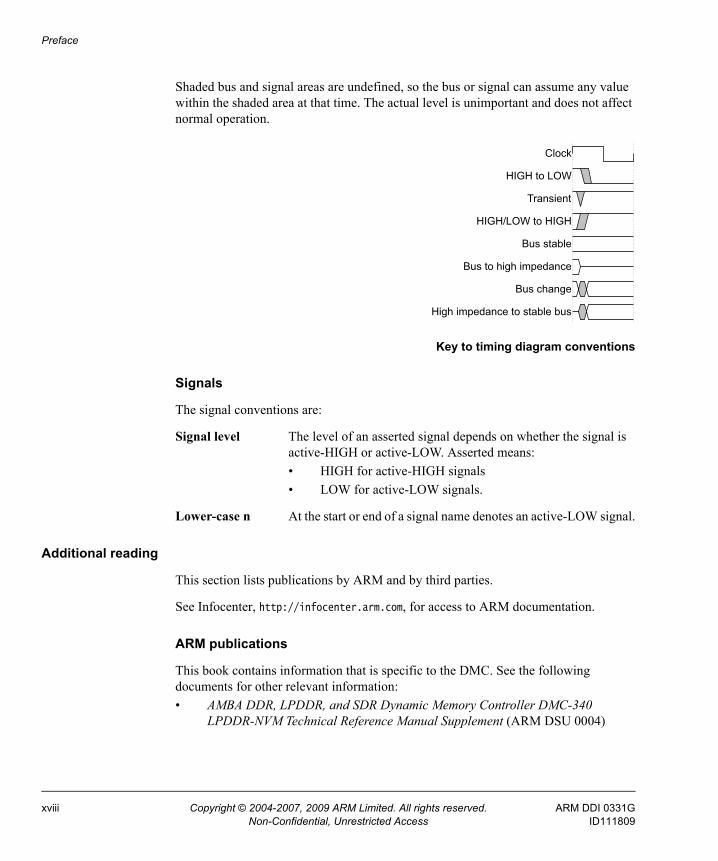
The figure named Key to timing diagram conventions on page xviii explains the components used in timing diagrams. Variations, when they occur, have clear labels. You must not assume any timing information that is not explicit in the diagrams.
ARM DDI 0331G Copyright © 2004-2007, 2009 ARM Limited. All rights reserved. xviiID111809 Non-Confidential, Unrestricted Access
Preface
Shaded bus and signal areas are undefined, so the bus or signal can assume any value within the shaded area at that time. The actual level is unimportant and does not affect normal operation.
Key to timing diagram conventions
Signals
The signal conventions are:
Signal level The level of an asserted signal depends on whether the signal is active-HIGH or active-LOW. Asserted means:• HIGH for active-HIGH signals• LOW for active-LOW signals.
Lower-case n At the start or end of a signal name denotes an active-LOW signal.
Additional reading
This section lists publications by ARM and by third parties.
See Infocenter, http://infocenter.arm.com, for access to ARM documentation.
ARM publications
This book contains information that is specific to the DMC. See the following documents for other relevant information:• AMBA DDR, LPDDR, and SDR Dynamic Memory Controller DMC-340
LPDDR-NVM Technical Reference Manual Supplement (ARM DSU 0004)
Clock
HIGH to LOW
Transient
HIGH/LOW to HIGH
Bus stable
Bus to high impedance
Bus change
High impedance to stable bus
xviii Copyright © 2004-2007, 2009 ARM Limited. All rights reserved. ARM DDI 0331GNon-Confidential, Unrestricted Access ID111809
Preface
Note This book is only delivered if you license the Low-Power Double Data
Rate-Non-Volatile Memory (LPDDR NVM) add-on.
• AMBA DDR, LPDDR, and SDR Dynamic Memory Controller DMC-340 Integration Manual (ARM DII 0105)
• AMBA DDR, LPDDR, and SDR Dynamic Memory Controller DMC-340 Implementation Guide (ARM DII 0106)
• AMBA DDR, LPDDR, and SDR Dynamic Memory Controller DMC-340 Supplement to AMBA Designer (ADR-301) User Guide (ARM DSU 0005)
• AMBA Designer (ADR-301) User Guide (ARM DUI 0333)• ARM PrimeCell® External Bus Interface (PL220) Technical Reference Manual
(ARM DDI 0249)• Integrating an External Bus Interface (PL220) with PL3xx Memory Controllers
Application Note (ARM DAI 0184)• AMBA AXI Protocol Specification (ARM IHI 0022)• AMBA 3 APB Protocol Specification (ARM IHI 0024)• AMBA DDR, LPDDR, and SDR Dynamic Memory Controller DMC-340 Release
Note.
Other publications
This section lists relevant documents published by third parties:• DDR PHY Interface (DFI) Specification, http://www.ddr-phy.org• JEDEC STANDARD Double Data Rate (DDR) SDRAM Specification, JESD79,
http://www.jedec.org
• JEDEC STANDARD Low Power Double Data Rate (LPDDR) SDRAM Specification, JESD209, http://www.jedec.org
• JEDEC STANDARD LPDDR-NVM Specification, http://www.jedec.org.
ARM DDI 0331G Copyright © 2004-2007, 2009 ARM Limited. All rights reserved. xixID111809 Non-Confidential, Unrestricted Access
Preface
FeedbackARM welcomes feedback on this product and its documentation.
Feedback on this product
If you have any comments or suggestions about this product, contact your supplier and give:• The product name.• The product revision or version.• An explanation with as much information as you can provide. Include symptoms
and diagnostic procedures if appropriate.
Feedback on content
If you have comments on content then send an e-mail to [email protected]. Give:• the title• the number, ARM DDI 0331G• the page numbers to which your comments apply• a concise explanation of your comments.
ARM also welcomes general suggestions for additions and improvements.
xx Copyright © 2004-2007, 2009 ARM Limited. All rights reserved. ARM DDI 0331GNon-Confidential, Unrestricted Access ID111809
Chapter 1 Introduction
This chapter introduces the DMC and contains the following sections:• About the DMC on page 1-2• Product revisions on page 1-6.
Note The DMC product designator is either PL340 or DMC-340 and depends on the product revision as follows:
r0p0 - r3p0 PL340.
r4p0 or later DMC-340.
ARM DDI 0331G Copyright © 2004-2007, 2009 ARM Limited. All rights reserved. 1-1ID111809 Non-Confidential, Unrestricted Access
Introduction
1.1 About the DMCThe DMC is an Advanced Microcontroller Bus Architecture (AMBA) compliant that is developed, tested, and licensed by ARM.
The DMC is a high-performance, area-optimized SDRAM or Mobile SDR memory controller compatible with the AMBA AXI protocol.
You can configure the DMC with a number of options, for example:• the SDRAM or Mobile SDR memory type• the number of SDRAM or Mobile SDR memory devices• the maximum SDRAM or Mobile SDR memory width• the number of outstanding AXI addresses• the pad interface type, for connection to the PHYsical (PHY) device.
For a complete list of the configurable options, see Features of the DMC on page 1-3.
Note For differences between revisions, see Product revisions on page 1-6.
The DMC supports the PrimeCell (PL220) External Bus Interface (EBI). This ensures that you can still use a shared external bus.
For more information about AMBA, see:• AMBA AXI Protocol Specification• AMBA 3 APB Protocol Specification.
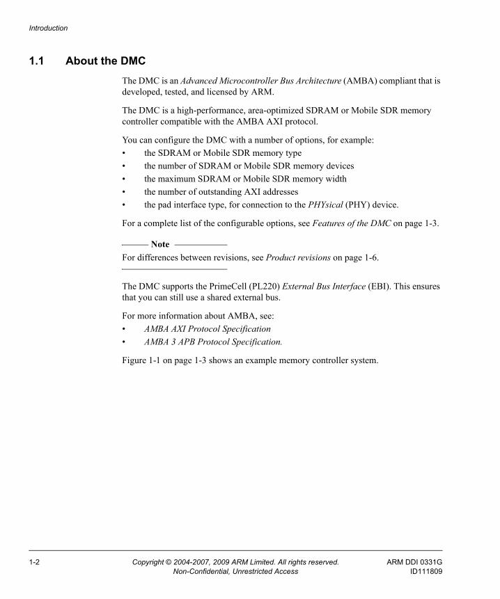
Figure 1-1 on page 1-3 shows an example memory controller system.
1-2 Copyright © 2004-2007, 2009 ARM Limited. All rights reserved. ARM DDI 0331GNon-Confidential, Unrestricted Access ID111809
Introduction
Figure 1-1 Example system
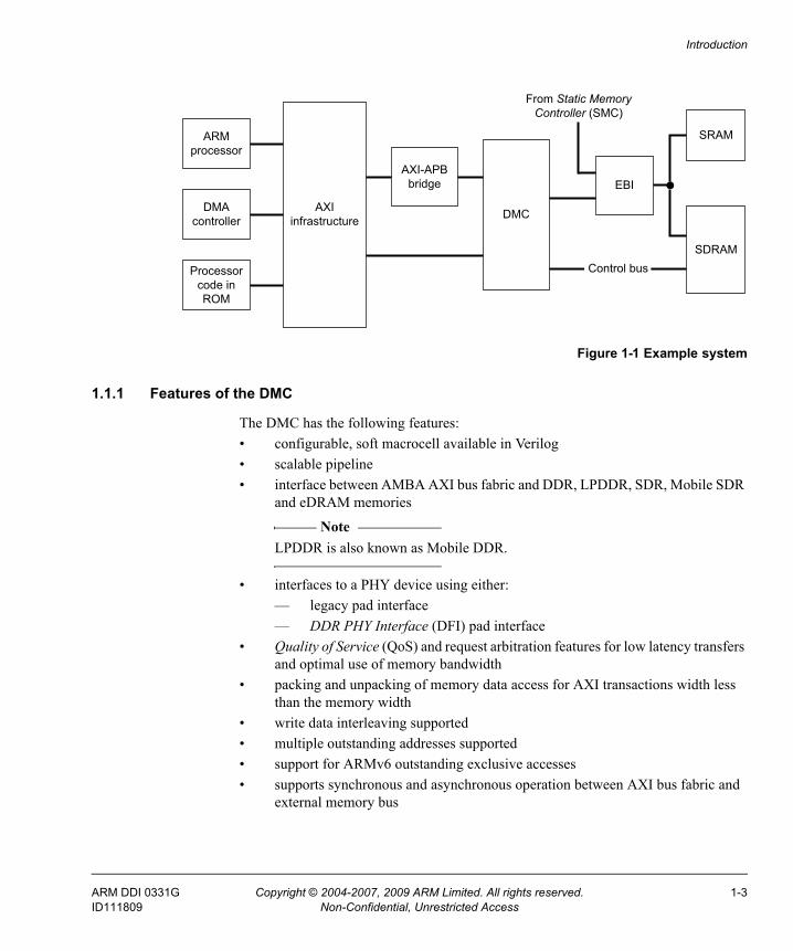
1.1.1 Features of the DMC
The DMC has the following features:• configurable, soft macrocell available in Verilog• scalable pipeline• interface between AMBA AXI bus fabric and DDR, LPDDR, SDR, Mobile SDR
and eDRAM memories
Note LPDDR is also known as Mobile DDR.
• interfaces to a PHY device using either:— legacy pad interface— DDR PHY Interface (DFI) pad interface
• Quality of Service (QoS) and request arbitration features for low latency transfers and optimal use of memory bandwidth
• packing and unpacking of memory data access for AXI transactions width less than the memory width
• write data interleaving supported• multiple outstanding addresses supported• support for ARMv6 outstanding exclusive accesses• supports synchronous and asynchronous operation between AXI bus fabric and
external memory bus
AXI-APB bridge EBI
AXI infrastructure
ARM processor
DMA controller
Processor code in ROM
SDRAM
SRAM
Control bus
DMC
From Static Memory Controller (SMC)
ARM DDI 0331G Copyright © 2004-2007, 2009 ARM Limited. All rights reserved. 1-3ID111809 Non-Confidential, Unrestricted Access
Introduction
Note Synchronous relates to rising edge-aligned clocks.
• programmable support for memory power saving modes including Deep Power-Down (DPD), active power-down, precharge power-down and self-refresh
• programmable through the AMBA APB interface• synchronous n:1 between AXI and APB when the clocks are rising edge-aligned• area and performance optimization, trade-offs through configurable hardware
resources• optimized utilization of external memory bus• one to four external chip selects• configurable for either a single cke signal for all chip selects or a separate cke
signal for each chip select• configurable bus width for the arid, awid, bid, rid, and wid signals• configurable bus width for the user_status, user_config, and user_config1
signals.
1.1.2 Supported memory widths
The DMC can support memory data bus widths of 16-bit, 32-bit, or 64-bit. However, during configuration of the DMC then it might not permit all of these options depending on the:• Configured AXI data bus width.• Type of memory device, SDR or DDR, that the DMC controls. When the DMC
controls:SDR devices The memory data bus width must not be less than half of the
AXI data bus width.DDR devices The memory data bus width must not be less than one
quarter of the AXI data bus width, and no greater than the AXI data bus width.
1-4 Copyright © 2004-2007, 2009 ARM Limited. All rights reserved. ARM DDI 0331GNon-Confidential, Unrestricted Access ID111809
Introduction
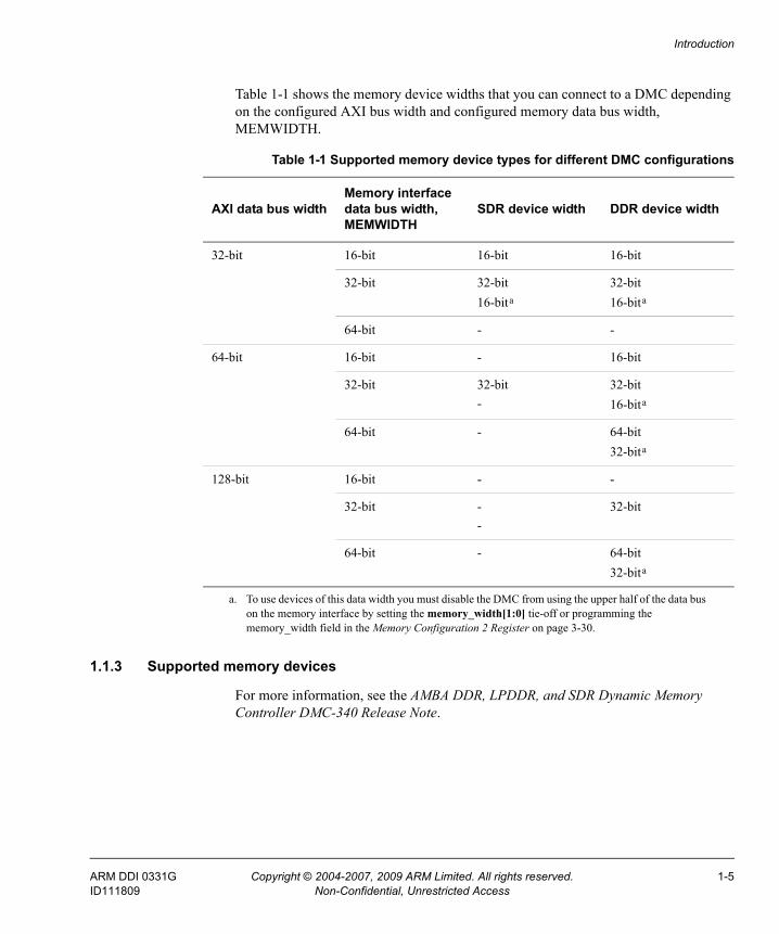
Table 1-1 shows the memory device widths that you can connect to a DMC depending on the configured AXI bus width and configured memory data bus width, MEMWIDTH.
1.1.3 Supported memory devices
For more information, see the AMBA DDR, LPDDR, and SDR Dynamic Memory Controller DMC-340 Release Note.
Table 1-1 Supported memory device types for different DMC configurations
AXI data bus widthMemory interface data bus width, MEMWIDTH
SDR device width DDR device width
32-bit 16-bit 16-bit 16-bit
32-bit 32-bit16-bita
32-bit16-bita
64-bit - -
64-bit 16-bit - 16-bit
32-bit 32-bit-
32-bit16-bita
64-bit - 64-bit32-bita
128-bit 16-bit - -
32-bit --
32-bit
64-bit - 64-bit32-bita
a. To use devices of this data width you must disable the DMC from using the upper half of the data bus on the memory interface by setting the memory_width[1:0] tie-off or programming the memory_width field in the Memory Configuration 2 Register on page 3-30.
ARM DDI 0331G Copyright © 2004-2007, 2009 ARM Limited. All rights reserved. 1-5ID111809 Non-Confidential, Unrestricted Access
Introduction
1.2 Product revisionsThis section summarizes the differences in functionality between the product revisions:
r0p0 - r1p0 This release includes a new configurable part.
r1p0 - r2p0 This release includes:• New configurable options:
— configuration that is programmable to support SDR, Mobile SDR, DDR, and LPDDR memory types
— eDRAM configuration— a global cke signal or a local cke signal for each memory
device— scalable pipeline— low-power modes of operation.
• New programmable options:— DPD support— variable number of auto-refresh requests before priority
change.• New functionality:
— improved write termination— programmable read_delay.
r2p0 - r3p0 This release includes optional NVM functionality.
r3p0 - r4p0 This release includes:• the option to configure the DMC to support a DFI pad interface, see
Pad interface on page 2-33• the ability to move all memory devices to deep power-down mode,
see Deep Power-Down on page 2-46• addition of user_config1 signals and User Config1 Register on
page 3-42• addition of the read_transfer_delay Register which controls the
number of idle cycles for back to back reads, see Read Transfer Delay Register on page 3-37
• addition of the feature_ctrl Register which controls the early write response behavior, see Feature Control Register on page 3-43
• configurable bus width for the user_status, user_config, and user_config1 signals, see User signals on page A-5
1-6 Copyright © 2004-2007, 2009 ARM Limited. All rights reserved. ARM DDI 0331GNon-Confidential, Unrestricted Access ID111809
Introduction
• configurable bus width for the arid, awid, bid, rid, and wid signals, see AXI signals on page A-6.
ARM DDI 0331G Copyright © 2004-2007, 2009 ARM Limited. All rights reserved. 1-7ID111809 Non-Confidential, Unrestricted Access

Introduction
1-8 Copyright © 2004-2007, 2009 ARM Limited. All rights reserved. ARM DDI 0331GNon-Confidential, Unrestricted Access ID111809
Chapter 2 Functional Description
This chapter describes the DMC operation. It contains the following sections:• Functional overview on page 2-2• Functional operation on page 2-10.
ARM DDI 0331G Copyright © 2004-2007, 2009 ARM Limited. All rights reserved. 2-1ID111809 Non-Confidential, Unrestricted Access
Functional Description
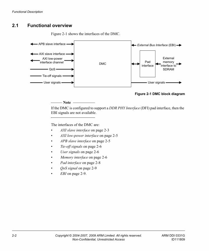
2.1 Functional overviewFigure 2-1 shows the interfaces of the DMC.
Figure 2-1 DMC block diagram
Note If the DMC is configured to support a DDR PHY Interface (DFI) pad interface, then the EBI signals are not available.
The interfaces of the DMC are:• AXI slave interface on page 2-3• AXI low-power interface on page 2-5• APB slave interface on page 2-5• Tie-off signals on page 2-6• User signals on page 2-6• Memory interface on page 2-6• Pad interface on page 2-8• QoS signal on page 2-9• EBI on page 2-9.
Pad interface
AXI slave interface AXI low-power
interface channel
APB slave interface
QoS
Tie-off signals
External Bus Interface (EBI)
User signals User signals
DMC
External memory
interface to SDRAM
2-2 Copyright © 2004-2007, 2009 ARM Limited. All rights reserved. ARM DDI 0331GNon-Confidential, Unrestricted Access ID111809
Functional Description
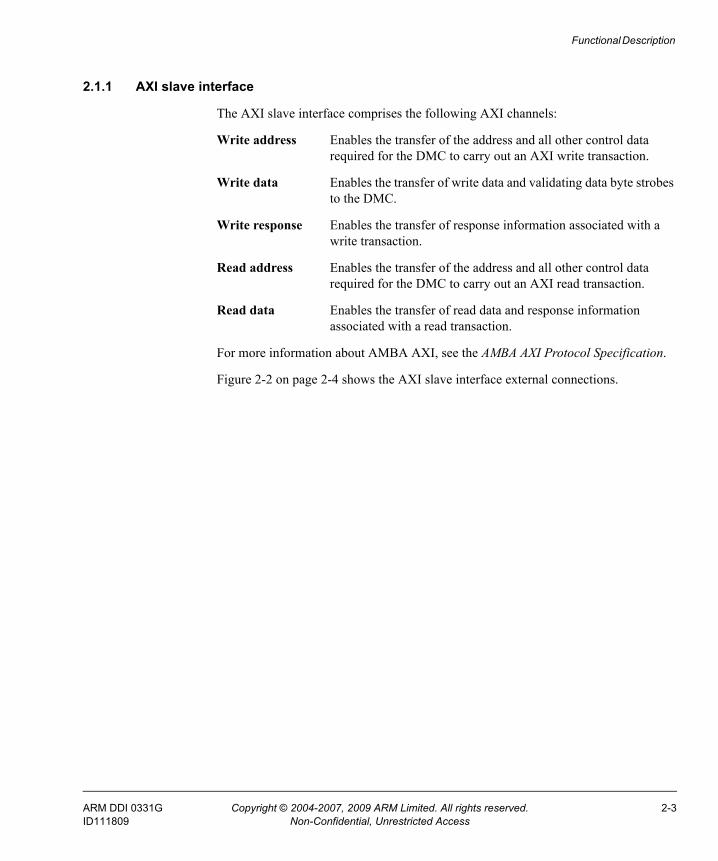
2.1.1 AXI slave interface
The AXI slave interface comprises the following AXI channels:
Write address Enables the transfer of the address and all other control data required for the DMC to carry out an AXI write transaction.
Write data Enables the transfer of write data and validating data byte strobes to the DMC.
Write response Enables the transfer of response information associated with a write transaction.
Read address Enables the transfer of the address and all other control data required for the DMC to carry out an AXI read transaction.
Read data Enables the transfer of read data and response information associated with a read transaction.
For more information about AMBA AXI, see the AMBA AXI Protocol Specification.
Figure 2-2 on page 2-4 shows the AXI slave interface external connections.
ARM DDI 0331G Copyright © 2004-2007, 2009 ARM Limited. All rights reserved. 2-3ID111809 Non-Confidential, Unrestricted Access
Functional Description
Figure 2-2 AXI slave interface connections
Global signals aclk
aresetn
Read addresschannel
arvalid
araddr[31:0] arlen[3:0] arsize[2:0]
arburst[1:0] arlock[1:0]
arcache[3:0] arprot[2:0]
arid[AID_WIDTH–1:0]
arready
Write addresschannel
awvalid
awaddr[31:0] awlen[3:0] awsize[2:0]
awburst[1:0] awlock[1:0]
awcache[3:0] awprot[2:0]
awid[AID_WIDTH–1:0]
awready
Write datachannel
wvalid wlast
wdata[AXI_DATA_MSB:0] wstrb[AXI_STRB_MSB:0]
wid[AID_WIDTH–1:0]
wready
Write responsechannel
bvalid bresp[1:0]
bid[AID_WIDTH–1:0] bready
Read datachannel
rvalid rlast
rdata[AXI_DATA_MSB:0] rresp[1:0]
rid[AID_WIDTH–1:0]
rready
2-4 Copyright © 2004-2007, 2009 ARM Limited. All rights reserved. ARM DDI 0331GNon-Confidential, Unrestricted Access ID111809
Functional Description
Note The arcache and arprot signals are included in the AXI slave interface, only for completeness. The DMC ignores any information that these signals provide.
For more information, see AXI slave interface on page 2-11.
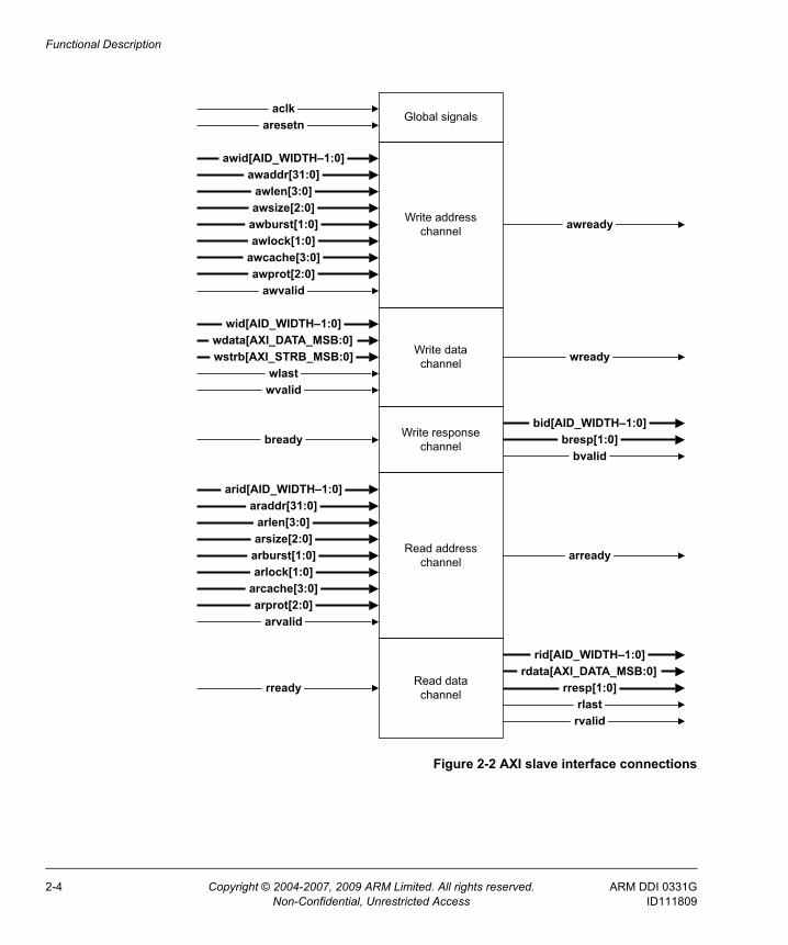
2.1.2 AXI low-power interface
Figure 2-3 shows the AXI low-power interface channel signals.
Figure 2-3 AXI low-power interface channel signals
For more information, see AXI low-power interface on page 2-16.
2.1.3 APB slave interface
The APB slave interface provides access to the internal registers of the DMC. Figure 2-4 shows the APB interface external connections.
Figure 2-4 APB signals
Note The pslverr output is included for completeness, and the DMC permanently drives it LOW.
For more information, see APB slave interface on page 2-17.
AXI low-power interface channel cactive csysreq
csysack cclken
APB pclken
paddr[31:0]
pwdata[31:0] pwrite
psel penable
prdata[31:0] pready pslverr
aclk
ARM DDI 0331G Copyright © 2004-2007, 2009 ARM Limited. All rights reserved. 2-5ID111809 Non-Confidential, Unrestricted Access
Functional Description
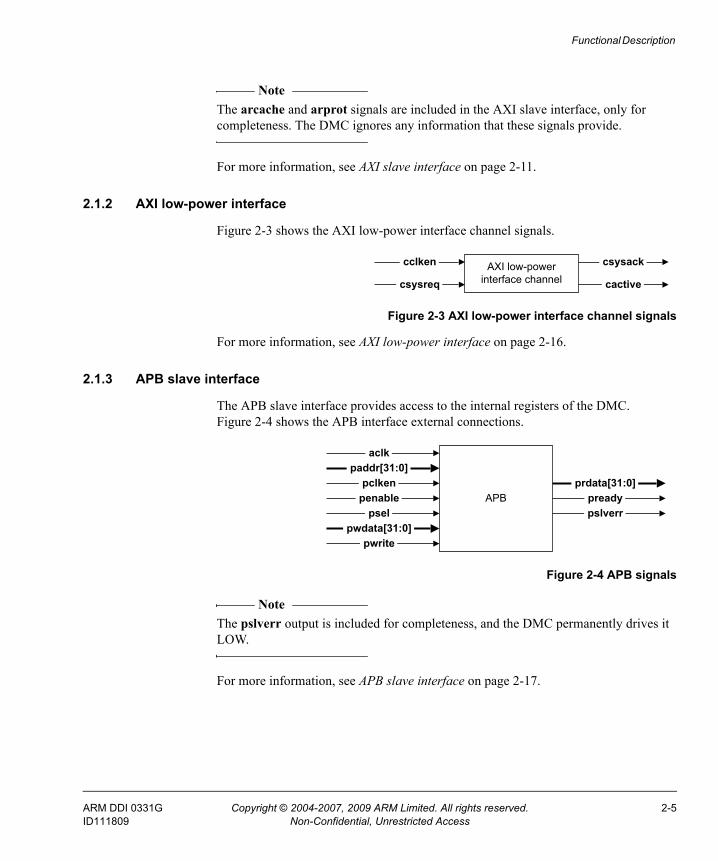
2.1.4 Tie-off signals
The tie-off signals initialize various operating parameters of the DMC when it exits the reset state. Figure 2-5 shows the tie-off signals.
Figure 2-5 Tie-off signals
For more information, see Tie-off signals on page 2-18.
2.1.5 User signals
The user signals are general purpose input and output signals that you can control and monitor by using the registers that the DMC provides. Figure 2-6 shows the user signals.
Figure 2-6 User signals
For more information, see Miscellaneous signals on page 2-18.
2.1.6 Memory interface
The memory interface provides a clean and defined interface between the arbiter and the pad interface, ensuring that the external memory interface command protocols are met in accordance with the programmed timings in the register block. See Chapter 3 Programmers Model.
The external inputs and outputs to this block are:
mclk Clock for mclk domain.
mresetn Reset for mclk domain. This signal is active LOW.
ebibackoff Tie this LOW to indicate that the DMC must not back off from the bus, if you are not using an External Bus Interface (EBI).
Tie-offs
a_gt_m_sync
memory_width[1:0]
cke_init dqm_init
memory_type[2:0]
sync read_delay[1:0]
user_status[USER_STATUS_WIDTH–1:0] user_config[USER_CONFIG_WIDTH–1:0]
DMC user_config1[USER_CONFIG_WIDTH–1:0]
2-6 Copyright © 2004-2007, 2009 ARM Limited. All rights reserved. ARM DDI 0331GNon-Confidential, Unrestricted Access ID111809
Functional Description
ebigrant Tie this HIGH to indicate that the bus is always granted, if you are not using an EBI.
ebireq Leave this unconnected, if you are not using an EBI.
use_ebi Tie this LOW, if you are not using an EBI.
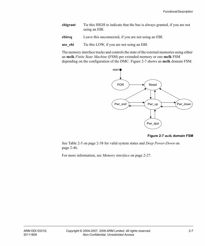
The memory interface tracks and controls the state of the external memories using either an mclk Finite State Machine (FSM) per extended memory or one mclk FSM depending on the configuration of the DMC. Figure 2-7 shows an mclk domain FSM.
Figure 2-7 mclk domain FSM
See Table 2-5 on page 2-38 for valid system states and Deep Power-Down on page 2-46.
For more information, see Memory interface on page 2-27.
start
Pwr_downPwr_upPwr_sref
POR Reset
Pwr_dpd
ARM DDI 0331G Copyright © 2004-2007, 2009 ARM Limited. All rights reserved. 2-7ID111809 Non-Confidential, Unrestricted Access
Functional Description
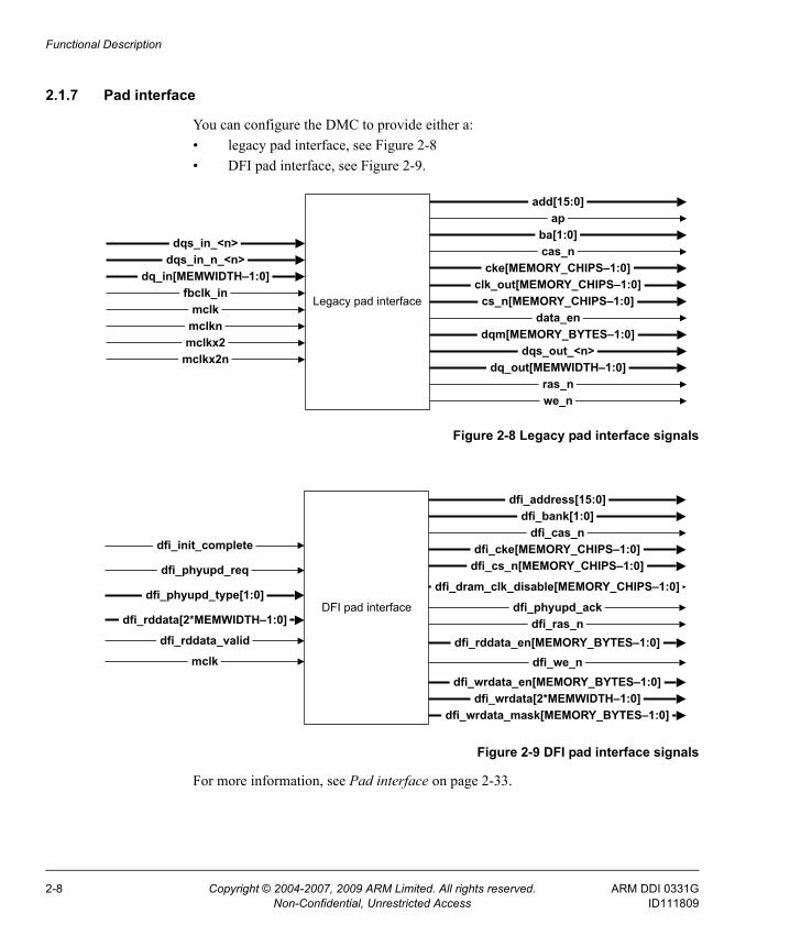
2.1.7 Pad interface
You can configure the DMC to provide either a:• legacy pad interface, see Figure 2-8• DFI pad interface, see Figure 2-9.
Figure 2-8 Legacy pad interface signals
Figure 2-9 DFI pad interface signals
For more information, see Pad interface on page 2-33.
Legacy pad interface data_en
dqs_in_<n>
fbclk_in
ras_n
ap
cs_n[MEMORY_CHIPS–1:0]
dqs_in_n_<n>
ba[1:0] cas_n
we_n
dqm[MEMORY_BYTES–1:0]
add[15:0]
dqs_out_<n> dq_out[MEMWIDTH–1:0]
clk_out[MEMORY_CHIPS–1:0]
mclk mclkn mclkx2
mclkx2n
dq_in[MEMWIDTH–1:0] cke[MEMORY_CHIPS–1:0]
DFI pad interface
dfi_init_complete
dfi_phyupd_req
dfi_bank[1:0] dfi_cas_n
dfi_address[15:0]
dfi_rddata_en[MEMORY_BYTES–1:0] dfi_rddata_valid
dfi_phyupd_type[1:0]
dfi_rddata[2*MEMWIDTH–1:0] dfi_phyupd_ack
dfi_ras_n
dfi_we_n dfi_wrdata_en[MEMORY_BYTES–1:0]
dfi_wrdata[2*MEMWIDTH–1:0] dfi_wrdata_mask[MEMORY_BYTES–1:0]
mclk
dfi_cke[MEMORY_CHIPS–1:0] dfi_cs_n[MEMORY_CHIPS–1:0]
dfi_dram_clk_disable[MEMORY_CHIPS–1:0]
2-8 Copyright © 2004-2007, 2009 ARM Limited. All rights reserved. ARM DDI 0331GNon-Confidential, Unrestricted Access ID111809
Functional Description
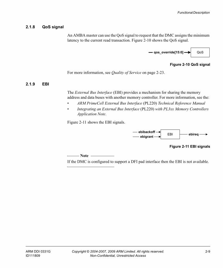
2.1.8 QoS signal
An AMBA master can use the QoS signal to request that the DMC assigns the minimum latency to the current read transaction. Figure 2-10 shows the QoS signal.
Figure 2-10 QoS signal
For more information, see Quality of Service on page 2-23.
2.1.9 EBI
The External Bus Interface (EBI) provides a mechanism for sharing the memory address and data buses with another memory controller. For more information, see the: • ARM PrimeCell External Bus Interface (PL220) Technical Reference Manual• Integrating an External Bus Interface (PL220) with PL3xx Memory Controllers
Application Note.
Figure 2-11 shows the EBI signals.
Figure 2-11 EBI signals
Note If the DMC is configured to support a DFI pad interface then the EBI is not available.
QoS qos_override[15:0]
ebigrant ebireq
ebibackoff EBI
ARM DDI 0331G Copyright © 2004-2007, 2009 ARM Limited. All rights reserved. 2-9ID111809 Non-Confidential, Unrestricted Access
Functional Description
2.2 Functional operationThis section describes:• Clocking and resets• AXI slave interface on page 2-11• AXI low-power interface on page 2-16• APB slave interface on page 2-17• Tie-off signals on page 2-18• Miscellaneous signals on page 2-18• Controller management operations on page 2-18• Data operations on page 2-21• Memory interface on page 2-27• Pad interface on page 2-33• Initialization on page 2-34• Low-power operation on page 2-37• TrustZone technology support on page 2-48.
2.2.1 Clocking and resets
This section describes:• Clocking• Reset on page 2-11.
Clocking
The DMC has the following functional clock inputs:• aclk• mclk• mclkn• mclkx2• mclkx2n• dqs_in_<n> where n is 0<n<bytes of external memory data bus• dqs_in_n_<n> where n is 0<n<bytes of external memory data bus.
Note mclkn, mclkx2, mclkx2n, dqs_in_<n>, and dqs_in_n_<n> are only available, if the DMC is configured to contain a legacy pad interface.
2-10 Copyright © 2004-2007, 2009 ARM Limited. All rights reserved. ARM DDI 0331GNon-Confidential, Unrestricted Access ID111809
Functional Description
These clocks can be grouped into two clock domains:
aclk domain aclk is in this domain. The aclk domain signals can only be stopped if the external memories are put in self-refresh mode.
mclk domain All clocks except aclk are in this domain. The mclk signal must be clocked at the rate of the external memory clock speed. The mclk domain signals can only be stopped if the external memories are put in self-refresh mode.
Note When configured with a legacy pad interface, the DMC provides a separate clock output for each external memory device.
Reset
The DMC has two reset inputs:aresetn This is the reset signal for the aclk domain.mresetn This is the reset signal for the mclk domain.
You can change both reset signals asynchronously to their respective clock domain. Internally to the DMC, the deassertion of the aresetn signal is synchronized to aclk, and the deassertion of the mresetn signal is synchronized to:• mclk for a DMC configured with DFI• the mclk, mclkn, mclkx2, and mclkx2n clock signals for a DMC configured with
a legacy pad interface.
2.2.2 AXI slave interface
The AXI programmers view is of a flat area of memory. The full range of AXI operations are supported, provided that the memory burst length selected is less than the read data FIFO depth.
Note • The read data FIFO depth and write data buffer depth are set during the
configuration process. For more information, see the AMBA DDR, LPDDR, and SDR Dynamic Memory Controller DMC-340 Supplement to AMBA Designer (ADR-301) User Guide.
ARM DDI 0331G Copyright © 2004-2007, 2009 ARM Limited. All rights reserved. 2-11ID111809 Non-Confidential, Unrestricted Access
Functional Description
• Refreshes can be missed if rready is held LOW, or the External Bus Interface (EBI) is not granted, for longer than one refresh period and the read data FIFO, command FIFO, and the arbiter queue become full. An OVL error triggers if this occurs in simulation. Ensure that the device has a sufficiently high system priority to prevent this.
If the AXI write data channel width is less than the memory data bus transfer rate, then to minimize memory accesses the DMC delays the memory access, when possible, until it can transfer the maximum number of data bits to the memory device. If the AXI read data channel width is less than the memory data bus transfer rate, then after the DMC reads the memory device it buffers the data to minimize the number of memory accesses. The memory data bus transfer rate is MEMWIDTH for SDR devices and 2×MEMWIDTH for DDR devices.
This section describes:• AXI slave interface attributes• Early BRESP on page 2-13• Memory device base address on page 2-13• Formatting from AXI address channels on page 2-14• Exclusive access on page 2-14.
AXI slave interface attributes
Table 2-1 shows the AXI slave attributes and their values.
Table 2-1 AXI slave interface attributes
Attributea
a. See Glossary for a description of these AXI attributes.
Value
Combined acceptance capability
Arbiter queue depth
Read acceptance capability
Read data reorder depth
Read interleave depth
Write acceptance capability
Write interleave depth
2-12 Copyright © 2004-2007, 2009 ARM Limited. All rights reserved. ARM DDI 0331GNon-Confidential, Unrestricted Access ID111809
Functional Description
If you connect the AXI slave interface of the DMC to the PrimeCell Interconnect (PL301) then the following AXI attributes in the PrimeCell Interconnect master interface require configuring:
Write issuing capability Set this to the value of the arbiter queue depth, or less. This ensures that the write acceptance capability of the DMC is not exceeded.
Write interleave capability Set this to the value of the arbiter queue depth, or less. This ensures that the write interleave depth of the DMC is not exceeded.
Note • When using the AMBA Designer application to configure a master interface on
the PrimeCell Interconnect (PL301), because AMBA Designer refers to the parameters of an attached slave then you set the write acceptance capability and write interleave depth. AMBA Designer uses the value entered to set the write issuing capability and write interleave capability of the PrimeCell Interconnect.
• The other attributes that Table 2-1 on page 2-12 shows are not applicable when configuring a PrimeCell Interconnect (PL301).
Early BRESP
To enable early write response timing, the DMC employs write data buffering and can issue the BRESP transfer before the data has been committed to the memory device. The response is sent after the last data beat is accepted by the AXI slave interface and stored in the write data buffer. You can enable this feature by programming the Feature Control Register on page 3-43. The controller have to maintain the coherency for read after write and write after write hazards to comply with the AXI ordering model.
Note For exclusive write accesses, the controller only issues a BRESP transfer after the write transaction is committed to a memory device.
Memory device base address
The base addresses of the external memory devices are programmable using the chip_cfg<n> registers. See Chip Configuration Register on page 3-39.
ARM DDI 0331G Copyright © 2004-2007, 2009 ARM Limited. All rights reserved. 2-13ID111809 Non-Confidential, Unrestricted Access
Functional Description
Formatting from AXI address channels
Formatting is as follows:
Chip select decoding The DMC compares an incoming address on araddr[31:24], or awaddr[31:24], with each address_match field programmed in the chip_cfg<n> registers. When a match occurs the DMC asserts chip select <n>. The address_mask field enables you to exclude some bits from the address comparison. See Chip Configuration Register on page 3-39.If no address match occurs then the DMC still performs the transfer but the result is undefined.
Row select decoding The AXI address determines the row address using bits [5:3] of the memory_cfg Register, and also the address_fmt bit for the selected chip defined in the chip_cfg<n> Register.
Column select decoding The AXI address determines the column address using bits [2:0] of the memory_cfg Register. See Memory Configuration Register on page 3-15.
Bank select decoding The AXI address determines the chip bank depending on the configuration of the DMC in addition to the address_fmt bit for the selected chip defined in the chip_cfg<n> Register.
Exclusive access
In addition to reads and writes, the DMC supports exclusive reads and writes in accordance with the AMBA AXI Protocol Specification.
Successful exclusive accesses have an EXOKAY response. All other accesses, including exclusive fail accesses, receive an OKAY response.
Exclusive access monitors implement the exclusive access functionality. Each monitor can track a single exclusive access. The number of monitors is a configurable option.
If an exclusive write fails, the data mask for the write is forced LOW, so that the data is not written.
When monitoring an exclusive access, the address of any write from another master is compared with the monitored address to check that the location is not being updated.
2-14 Copyright © 2004-2007, 2009 ARM Limited. All rights reserved. ARM DDI 0331GNon-Confidential, Unrestricted Access ID111809
Functional Description
For the purposes of monitoring, address comparison is made using a bit mask derived in the following fashion.
Consider the byte addresses accessed by a transaction. All the least significant bits, up to and including, the most significant bit that vary between those addresses are set to logic zero in the mask. All the stable address bits above this point are set to logic one.
Example 2-1 provides information about three transactions.
Example 2-1 Exclusive accesses
Exclusive Read Address = 0x100, size = WORD, length = 1, ID = 0.
Write Address = 0x104, size = WORD, length = 2, ID = 1.
Exclusive Write Address = 0x100, size = WORD, length = 1, ID = 0.
The write transaction accesses the address range 0x104-0x10B. Therefore, address bit 3 is the most significant bit that varies between byte addresses. The bit mask is therefore formed so that address bits 3 down to 0 are not compared. This has the effect that the masked write, as far as the monitoring logic has calculated, has accessed the monitored address. Therefore the exclusive write is marked as having failed.
Table 2-2 shows the address comparison steps.
Table 2-2 Address comparison steps example
Step Binary Hex
1 Monitored address b000100000000 0x100
2 Write address b000100000100 0x104
ARM DDI 0331G Copyright © 2004-2007, 2009 ARM Limited. All rights reserved. 2-15ID111809 Non-Confidential, Unrestricted Access
Functional Description
This example shows how the logic can introduce false-negatives in exclusive access monitoring, because in reality the write has not accessed the monitored address. The implementation has been chosen to reduce design complexity but always provide safe behavior.
When calculating the address region accessed by the write, the burst type is always taken to be INCR. Therefore, a wrapped transaction in Example 2-1 on page 2-15 that wraps down to 0x0 rather than cross the boundary, is treated in the same way. This is the same for a fixed burst that does not cross the boundary or wrap down to 0x0.
2.2.3 AXI low-power interface
The low-power interface can move the DMC into its Low_power state without the requirement for any register accesses, see aclk domain state diagram on page 2-19 and Low-power operation on page 2-37.
For more information about the AXI low-power interface, see the AMBA DDR, LPDDR, and SDR Dynamic Memory Controller DMC-340 Integration Manual.
If you do not require the low-power interface, tie it off.
3 Write accesses b000100000100 0x104
b000100000101 0x105
b000100000110 0x106
b000100000111 0x107
b000100001000 0x108
b000100001001 0x109
b000100001010 0x10A
b000100001011 0x10B
4 Generate a comparison mask b111111110000 0xFF0
5 Monitored address ANDed with mask b000100000000 0x100
6 Write address ANDed with mask b000100000000 0x100
7 Compare steps 5 and 6
8 Mark exclusive write as failed
Table 2-2 Address comparison steps example (continued)
Step Binary Hex
2-16 Copyright © 2004-2007, 2009 ARM Limited. All rights reserved. ARM DDI 0331GNon-Confidential, Unrestricted Access ID111809
Functional Description
2.2.4 APB slave interface
The APB interface is a fully compliant APB slave.
For more information about the AMBA APB, see the AMBA 3 APB Protocol Specification.
The APB interface enables you to access the operating state of the DMC and to program it with the correct timings and settings for the connected memory type. See Chapter 3 Programmers Model for more information. The APB interface also initializes the connected memory devices, see Initialization on page 2-34.
Note • The APB interface only supports 32-bit data accesses. The DMC ignores the
paddr[1:0] bits and therefore byte or halfword accesses are treated as word accesses.
• The pslverr output is included for completeness. The DMC ties it LOW.
The APB interface is clocked by the same clock as the AXI domain clock, aclk. The DMC provides a clock enable, pclken, enabling the APB interface to be slowed down and execute at an integer divisor of aclk.
To enable a clean registered interface to the external infrastructure, the APB interface always adds a wait state for all reads and writes by driving pready LOW. In the following instances, a delay of more than one wait state can be generated when a:• direct command is received and there are outstanding commands that prevent a
new command being stored in the command FIFO• memory command is received, and a previous memory command has not been
completed.
The only registers that can be accessed when the DMC is not in the Config or Low_power state are:• memc_status Register, to read the current state, see Memory Controller Status
Register on page 3-9• memc_cmd Register, to change state, see Memory Controller Command Register
on page 3-12.
To guarantee no missed AUTO REFRESH commands, it is recommended that any change of mclk period, and therefore update of the refresh period, is carried out when the DMC is in the Low_power state. This is because the refresh rate depends on the mclk period. You can only write direct commands to the external memories when the DMC is in the Config state and not in the Low_power state.
ARM DDI 0331G Copyright © 2004-2007, 2009 ARM Limited. All rights reserved. 2-17ID111809 Non-Confidential, Unrestricted Access
Functional Description
2.2.5 Tie-off signals
The DMC enables you to change some of its configuration settings by using the tie-off signals.
At reset, the value of each tie-off signal controls the respective bits in the memory_cfg2 Register.
After reset you can program the memory_cfg2 Register to make additional changes to these configuration settings. See Memory Configuration 2 Register on page 3-30.
2.2.6 Miscellaneous signals
You can use the following signals as general-purpose control signals for logic external to the DMC:
user_status[USER_STATUS_WIDTH–1:0] Use the user_status Register to read the status of these general purpose inputs. You must tie any unused signals to either HIGH or LOW. These signals are connected directly to the APB interface block. Therefore, if they are driven from external logic that is not clocked by the aclk signal, then external synchronization registers are required. See User Status Register on page 3-40.
user_config[USER_CONFIG_WIDTH–1:0] Use the user_config Register to control these general purpose outputs. If you do not require these signals, leave them unconnected. See User Config Register on page 3-41.
user_config1[USER_CONFIG_WIDTH–1:0] Use the user_config1 Register to control these general purpose outputs. If you do not require these signals, leave them unconnected. See User Config1 Register on page 3-42.
You can use the following miscellaneous signals for automatic test pattern generator testing of the DMC:• rst_bypass• dft_en_clk_out.
2.2.7 Controller management operations
The memory manager tracks and controls the current state of the DMC using the aclk Finite State Machine (FSM). You can change the state of the controller by programming the memc_cmd Register, see Memory Controller Command Register on page 3-12.
2-18 Copyright © 2004-2007, 2009 ARM Limited. All rights reserved. ARM DDI 0331GNon-Confidential, Unrestricted Access ID111809
Functional Description
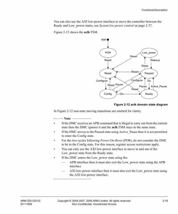
You can also use the AXI low-power interface to move the controller between the Ready and Low_power states, see System low-power control on page 2-37.
Figure 2-12 shows the aclk FSM.
Figure 2-12 aclk domain state diagram
In Figure 2-12 non-state moving transitions are omitted for clarity.
Note • If the DMC receives an APB command that is illegal to carry out from the current
state then the DMC ignores it and the aclk FSM stays in the same state.• If the DMC moves to the Paused state using Active_Pause then it is not permitted
to enter the Config state.• For the two cycles following Power-On-Reset (POR), do not consider the DMC
to be in the Config state. For this reason, register access restrictions apply.• You can only use the AXI low-power interface to move in and out of the
Low_power state from the Ready state.• If the DMC enters the Low_power state using the:
— APB interface then it must also exit the Low_power state using the APB interface
— AXI low-power interface then it must also exit the Low_power state using the AXI low-power interface.
Reset
ConfigureReset
Go
Go
Pause Active_Pause
Sleep
Wakeup
Reset
Reset
Reset
PauseConfigure
start
Reset
Config
Paused
Ready
Low_powerPOR
ARM DDI 0331G Copyright © 2004-2007, 2009 ARM Limited. All rights reserved. 2-19ID111809 Non-Confidential, Unrestricted Access
Functional Description
The current status of the aclk FSM controls the functionality of the DMC:• All the registers are available for writes or reads when the aclk FSM is in the
Config or Low_power state.• When in the Config state or Low_power state, no AUTO REFRESH commands are
generated. When the Low_power state is entered, the SDRAM memories are put into self-refresh mode.
• When in the Ready state, not all registers are available, see Chapter 3 Programmers Model.
• Move the DMC to the Paused state by programming the memc_cmd Register and selecting one of the following commands:— Pause command.
When a Pause is requested, then the Paused state is only entered when the DMC is idle.
— Active_Pause command.When an Active_Pause is requested then the Paused state is entered when the memory interface is idle but there might still be outstanding transactions in the arbiter queue.
Note No AUTO REFRESH commands are generated when in the Config state. If you are changing register values, it is necessary to enter the Low_power state, because this removes the risk of the memory maximum refresh time being exceeded.
The DMC management function can issue commands to the memory interface from one of the following sources:Direct commands
These are received over the APB interface as a result of a write to the direct_cmd Register. See Direct Command Register on page 3-13. They initialize the SDRAM.The legal commands that the memory manager uses are:• NOP
• PRECHARGEALL
• AUTO REFRESH
• MODEREG
• extended MODEREG• Deep Power-Down (DPD).
2-20 Copyright © 2004-2007, 2009 ARM Limited. All rights reserved. ARM DDI 0331GNon-Confidential, Unrestricted Access ID111809
Functional Description
Commands from the aclk FSM You can traverse the aclk FSM by writing to the memc_cmd Register. See Memory Controller Command Register on page 3-12. You can only traverse the aclk FSM states when the DMC is idle. For example, the Ready state can only be entered from the Config state when all direct commands have been completed. The exception to this is the Active_Pause command. You can issue this command when the DMC is active. When you issue the command, any memory accesses that have not been arbitrated remain in the arbiter until the aclk FSM receives the Go command.
Refresh commands The refresh logic can issue commands to the arbiter to refresh the SDRAM chips. The refresh counter is clocked by the memory clock to enable the frequency of the DMC to be scaled without affecting the refresh rate. The refresh rate period is programmable using the refresh_prd Register. See Refresh Period Register on page 3-19. The value of this register is the count value in mclk cycles.When the refresh counter wraps around zero, an individual auto-refresh sequence is requested for each external chip in turn.You can prevent Refresh commands from being generated by using the active_chips field in the memory_cfg Register. See Memory Configuration Register on page 3-15.
Note Refreshes are masked from the most significant chip number downwards.
These management commands are arbitrated with data commands.
2.2.8 Data operations
All data operations are carried out through the AXI slave interface.
The number of outstanding AXI transactions that can be processed is a configurable option. Each outstanding transaction is referred to as:• arbiter queue entries, or• entries.
An entry can be created for one of two functions:• data entries, as the result of AXI data transactions• management entries, as a result of management functions.
If there is a coincident data entry and management entry request, the management entry takes priority and delays the data entry by one clock cycle.
ARM DDI 0331G Copyright © 2004-2007, 2009 ARM Limited. All rights reserved. 2-21ID111809 Non-Confidential, Unrestricted Access
Functional Description
Entries are arbitrated with an algorithm that optimizes the efficiency of the external data bus. You can modify the algorithm to meet any programmed QoS requirement.
To achieve optimum memory bus efficiency entries might be arbitrated out of order from their arrival time. Entries that cannot be arbitrated because of hazards are removed from the algorithm until the hazard is cleared.
An arbiter queue entry might not be arbitrated continuously. If a QoS event occurs then the highest priority entry changes.
The following subsections describe:• Hazard detection• Quality of Service on page 2-23• Arbitration on page 2-25.
Hazard detection
The following types of hazard exist:
Read After Read (RAR) There is a read already in the arbiter queue with the same ID as the incoming entry, that is also a read.
Write After Write (WAW) There is a write already in the arbiter queue with the same ID as the incoming entry, that is also a write.There is a write in the arbiter queue that has received an early write response, accessing the same location as the incoming write.
Read After Write (RAW) There is a write in the arbiter queue, that has received an early write response, accessing the same location as the incoming read entry.
The arbiter entry is flagged as having a dependency if a hazard is detected. There might be dependencies against a number of other arbiter entries. As the arbiter entries are invalidated, so the dependencies are reduced until finally, there are no outstanding dependencies, and the entry is free to start.
Note There are no Write-After-Read (WAR) hazard checks in the DMC. If an AXI master requires ordering between reads and writes to certain memory locations, it must wait for read data before issuing a write to a location it has read from. Similarly, the only RAW
2-22 Copyright © 2004-2007, 2009 ARM Limited. All rights reserved. ARM DDI 0331GNon-Confidential, Unrestricted Access ID111809
Functional Description
hazard checking is that performed when the write response has been issued. If an AXI master required ordering between writes and reads to certain memory locations, it must wait for the write response before issuing the read to the same location.
Write transactions are also excluded from the arbitration algorithm until either:• a full memory burst worth of data is received• the write data burst completes• the write data buffer becomes full• write data with a different ID is received.
Quality of Service
QoS is defined for the DMC as a method of increasing the arbitration priority of a read access that requires low-latency read data. See Arbitration on page 2-25 for more information. The QoS for an AXI read access is determined when the arbiter receives it. No QoS exists for write accesses.
The following sections describe:• QoS selection• QoS timeout on page 2-24• QoS for AUTO REFRESH on page 2-24.
QoS selection
The allocation of QoS functionality is determined by the arid of the AXI transfer compared with a 4-bit selection mask defined by the qos_master_bits in the memory_cfg Register. You can program the 4-bit QoS mask to be either arid[3:0], arid[4:1], arid[5:2], arid[6:3], arid[7:4] arid[8:5], arid[9:6], or arid[10:7]. After the DMC applies the 4-bit QoS mask to the arid number, the resulting value <n> provides the pointer to which id_<n>_cfg Register contains the QoS settings for the read transfer.
For more information, see Memory Configuration Register on page 3-15 and QoS Configuration Register on page 3-38.
Example 2-2 on page 2-24 shows QoS selection and the impact of the qos_override signal.
ARM DDI 0331G Copyright © 2004-2007, 2009 ARM Limited. All rights reserved. 2-23ID111809 Non-Confidential, Unrestricted Access
Functional Description
Example 2-2 QoS selection and qos_override
If you program the qos_master_bits = b010 then this selects arid[5:2] to be the 4-bit QoS mask. If the DMC receives an AXI transfer with an arid of 0x5A then it applies the 4-bit QoS mask, arid[5:2], giving a value of 0x6. Therefore, the controller uses the id_6_cfg Register to control the QoS for the transfer.
The controller creates a new arbiter entry for the transfer and assigns it the qos_min and qos_max values from the id_6_cfg Register. If the qos_enable bit=1 then the controller applies the QoS settings to the transfer.
The qos_override[15:0] signal enables the controller to assign an arbiter entry with minimum QoS latency, irrespective of the state of the qos_enable bit. For this example, if qos_override[6] is HIGH when arvalid and arready are HIGH then the arbiter entry is assigned minimum QoS latency, even if the qos_enable bit=0.
QoS timeout
If the qos_enable bit for the arid is set in the register bank, the QoS maximum latency value is decremented every aclk cycle until it reaches zero.
If the entry is still in the queue when the QoS maximum latency value reaches zero, then the entry becomes high priority. This is called a timeout. Also, any entry in the queue with a minimum latency QoS also produces a timeout. Minimum latency timeouts have priority over maximum latency timeouts.
When an entry times out in this way it forces a timeout onto any entries that it has dependencies against. In normal operation, these entries have already timed out because they have received the same initial QoS value, but been decrementing for longer. The highest priority arbiter entry is serviced next.
One special case exists. This is when or if the assertion of the relevant qos_override signal forces a minimum latency timeout. In this instance, any accesses that the new entry has dependencies against might not have timed out and are forced to time out so that the high-priority entry can start as soon as possible. This can include when there is a read after write hazard, under which circumstance the writes ahead of the read must also be prioritized.
QoS for AUTO REFRESH
The DMC provides QoS for the AUTO REFRESH commands by using a simple increment-decrement counter to keep track of the number of AUTO REFRESH commands in the arbiter queue.
2-24 Copyright © 2004-2007, 2009 ARM Limited. All rights reserved. ARM DDI 0331GNon-Confidential, Unrestricted Access ID111809
Functional Description
The arbiter compares the counter to the value of the max_outs_refs field in the memory_cfg3 Register, see Memory Configuration 3 Register on page 3-34. When the counter reaches the max_outs_refs value then a refresh timeout is signaled to the arbiter queue.
A refresh timeout forces all of the AUTO REFRESH queue entries to timeout. This timeout is sticky, and does not disappear when the number of timeouts drops back below the max_outs_refs threshold. Instead, it remains asserted until the DMC services all of the AUTO REFRESH entries. This provides a guaranteed refresh rate in the SDRAM.
Arbitration
The arbitration algorithm, without considering QoS issues, operates in the following way:• bank preparation, that is, any memory operations to a closed row• read or write to open rows, that is, any memory operation to an open row• manager operations, for example, refreshes.
A particular queue item, that contains either one AXI transaction or manager operation, cannot appear in two groups. If a read transaction enters the queue to a closed row, it is made available to the arbiter as a bank preparation operation, and not a read hit. When the row has been opened, possibly after two bank preparation operations, it is flagged as a read hit.
A read to a closed row is split into:• a bank preparation• an open row read.
These are stored in the same arbiter queue slot.
Example 2-3 shows an arbitration example.
Example 2-3 Arbitration example
Assume chip 0 has recently been refreshed, all rows are closed, and nothing can be issued for t_rfc.
During t_rfc, the following transactions enter the queue, in the following order:1. Read, row 1 chip 0 bank 0, transaction 1.2. Read, row 1 chip 0 bank 0, transaction 2.3. Read, row 4 chip 0 bank 1, transaction 3.4. Write, row 1 chip 0 bank 0, transaction 4.
ARM DDI 0331G Copyright © 2004-2007, 2009 ARM Limited. All rights reserved. 2-25ID111809 Non-Confidential, Unrestricted Access
Functional Description
Nothing is arbitrated until t_rfc has expired.
The cycle numbers in this example can change depending on factors such as schedule delays, burst lengths, and the command FIFO depth. The following describes the behavior during each cycle:
Cycle 1 No transactions are marked as either read hit or write hit because all rows are closed. Instead, all transactions are marked as bank preparations. The oldest transaction is selected, and transaction 1, row 1 chip 0, bank 0 is marked as open in the row cache.
Cycle 2 Transactions 1, 2, and 4 are now open row reads or writes. However, because the ACTIVE command has only recently been issued, they are not available to the arbiter until schedule_rcd expires. The arbiter therefore selects the next available bank preparation operation, because the refresh is the lowest priority. This is transaction 3.
Cycle 3 Transactions 1, 2, and 4 are flagged as read hits, or write hits, because the delay has now expired, assuming that schedule_rcd was set to 1. Because a bank preparation operation was performed in the last cycle, the oldest read hit now becomes the highest priority. Transaction 1 is therefore arbitrated and removed from the queue.
Cycle 4 Transactions 2, 3, and 4 are now available as read or write hits. The last cycle was a read operation so bank preparation operations are the highest priority. However, because there are none to perform, transaction 2 is arbitrated.Transaction 5 now arrives, read, row 1 chip 0 bank 0. Because row 1 chip 0 bank 0 is already open, it is flagged as a read hit immediately.
Cycle 5 Transactions 3, 4, and 5 are available as a read hits, or write hits. Transaction 3 is selected because it is the oldest transaction.Transaction 6 arrives, read, row 3 chip 0 bank 1. Because bank 1 row 4 is still open, this transaction is to a closed row.
Cycle 6 Transactions 4 and 5 are a write hit and read hit. Transaction 6 is a bank preparation operation. The last transactions were reads, so the bank preparation for transaction 6 is selected, and this issues a precharge because another row in the same bank was open.
Cycle 7 Transaction 4 is a write hit, transaction 5 is a read hit, and transaction 6 is unavailable while schedule_rp expires. The arbiter tries to maintain the data direction because this is more efficient on the memory bus. Transaction 5, a read, is therefore arbitrated.
2-26 Copyright © 2004-2007, 2009 ARM Limited. All rights reserved. ARM DDI 0331GNon-Confidential, Unrestricted Access ID111809
Functional Description
Cycle 8 Transaction 4 is a write hit, and transaction 6 is available as a bank preparation operation because all rows in the bank are closed. The last operation was a read, so the bank preparation operation is selected, transaction 6, and an ACTIVE command is issued.
Cycle 9 Transaction 4 is now a write hit and transaction 6 is unavailable while schedule_rcd expires. The arbiter chooses the only available operation and that is transaction 4. It is then removed from the queue.
Cycle 10 Transaction 6 is now a read hit, and is finally arbitrated as a read hit, and removed from the queue.
2.2.9 Memory interface
The memory interface is separated from the arbiter using the following configurable synchronous or asynchronous FIFOs and buffer:• command FIFO• read data FIFO• write data buffer.
Note Synchronous relates to rising edge-aligned clocks.
The memory interface reads commands from the arbiter using the command FIFO but only when that command can be executed. The memory interface ensures a command is only executed when all the inter-command delays, defined in this section, for that bank or memory device are met.
The memory interface enables multiple banks to be active at any one time. However, only one bank can be carrying out a data transfer at any one time. If the command at the head of the command FIFO cannot be executed, then the command pipeline stalls until it can be executed.
Scheduler
To reduce the occurrence of pipeline stalls, the DMC contains a scheduler that monitors the activity of the mclk FSMs in the memory interface. The scheduler uses the information in the schedule fields of the t_rcd, t_rfc and t_rp registers, to prevent the
ARM DDI 0331G Copyright © 2004-2007, 2009 ARM Limited. All rights reserved. 2-27ID111809 Non-Confidential, Unrestricted Access
Functional Description
arbiter from issuing commands that can stall the command pipeline. Program the schedule fields with the amount of delay you require, in aclk cycles. For synchronized 1:1 operation of aclk and mclk, program:• schedule_rcd = t_rcd–3 in the ACTIVE to Read or Write Timing Register on
page 3-23• schedule_rfc = t_rfc–3 in the AUTO REFRESH to Command Timing Register on
page 3-24• schedule_rp = t_rp–3 in the PRECHARGE to Command Timing Register on
page 3-25.
For non-synchronized 1:1 operation, you must scale the schedule_rx fields accordingly.
Note For the LPDDR NVM add-on, the nvm_schedule_rcd is applied when accessing NVM chips.
Memory interface to pad interface timing
All command control outputs are clocked on the falling edge of the memory clock, mclk. The relative times between control signals from the memory interface are maintained when output from the pad interface to the actual SDRAM devices. Therefore, the timing register values required for a particular SDRAM device can be determined from that SDRAM device’s data sheet.
Figure 2-13 on page 2-29 to Figure 2-24 on page 2-33 show how the data sheet timings map on to the DMC timing registers. Figure 3-2 on page 3-3 shows the timing registers.
Note In Figure 2-13 on page 2-29 to Figure 2-24 on page 2-33:• The following signals are internal to the DMC:
— command_en— data_cntl_en— memif_busy— pwr_down— read_en.
• The timings shown are not necessarily the default timing values but are values that are small enough to show the entire delay in one figure.
Figure 2-13 on page 2-29 shows the command control output timing.
2-28 Copyright © 2004-2007, 2009 ARM Limited. All rights reserved. ARM DDI 0331GNon-Confidential, Unrestricted Access ID111809
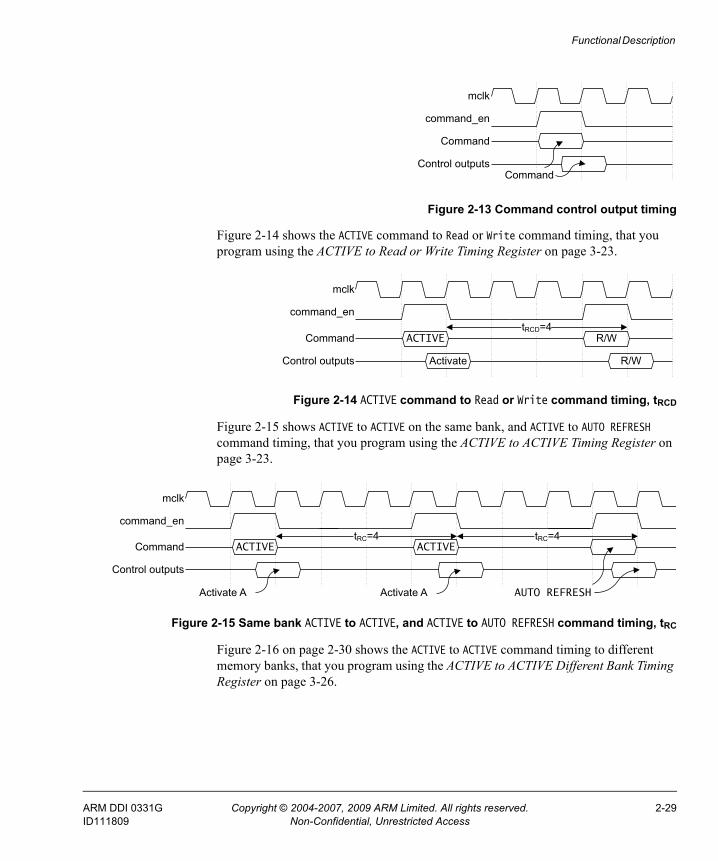
Functional Description
Figure 2-13 Command control output timing
Figure 2-14 shows the ACTIVE command to Read or Write command timing, that you program using the ACTIVE to Read or Write Timing Register on page 3-23.
Figure 2-14 ACTIVE command to Read or Write command timing, tRCD
Figure 2-15 shows ACTIVE to ACTIVE on the same bank, and ACTIVE to AUTO REFRESH command timing, that you program using the ACTIVE to ACTIVE Timing Register on page 3-23.
Figure 2-15 Same bank ACTIVE to ACTIVE, and ACTIVE to AUTO REFRESH command timing, tRC
Figure 2-16 on page 2-30 shows the ACTIVE to ACTIVE command timing to different memory banks, that you program using the ACTIVE to ACTIVE Different Bank Timing Register on page 3-26.
mclk
command_en
Command
Control outputsCommand
mclk
command_en
Command
Control outputs
ACTIVE R/WtRCD=4
Activate R/W
mclk
command_en
Command
Control outputs
tRC=4
Activate A
tRC=4
AUTO REFRESHActivate A
ACTIVE ACTIVE
ARM DDI 0331G Copyright © 2004-2007, 2009 ARM Limited. All rights reserved. 2-29ID111809 Non-Confidential, Unrestricted Access
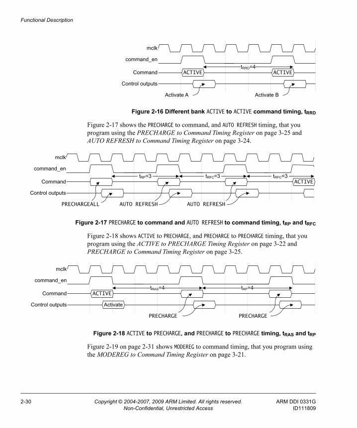
Functional Description
Figure 2-16 Different bank ACTIVE to ACTIVE command timing, tRRD
Figure 2-17 shows the PRECHARGE to command, and AUTO REFRESH timing, that you program using the PRECHARGE to Command Timing Register on page 3-25 and AUTO REFRESH to Command Timing Register on page 3-24.
Figure 2-17 PRECHARGE to command and AUTO REFRESH to command timing, tRP and tRFC
Figure 2-18 shows ACTIVE to PRECHARGE, and PRECHARGE to PRECHARGE timing, that you program using the ACTIVE to PRECHARGE Timing Register on page 3-22 and PRECHARGE to Command Timing Register on page 3-25.
Figure 2-18 ACTIVE to PRECHARGE, and PRECHARGE to PRECHARGE timing, tRAS and tRP
Figure 2-19 on page 2-31 shows MODEREG to command timing, that you program using the MODEREG to Command Timing Register on page 3-21.
mclk
command_en
Command
Control outputs
tRRD=4
Activate BActivate A
ACTIVE ACTIVE
tRFC=3
mclk
command_en
Command
Control outputs
tRP=3
AUTO REFRESH
tRFC=3
AUTO REFRESHPRECHARGEALL
ACTIVE
mclk
command_en
Command
Control outputs
ACTIVEtRAS=4
PRECHARGE
tRP=4
PRECHARGE
Activate
2-30 Copyright © 2004-2007, 2009 ARM Limited. All rights reserved. ARM DDI 0331GNon-Confidential, Unrestricted Access ID111809
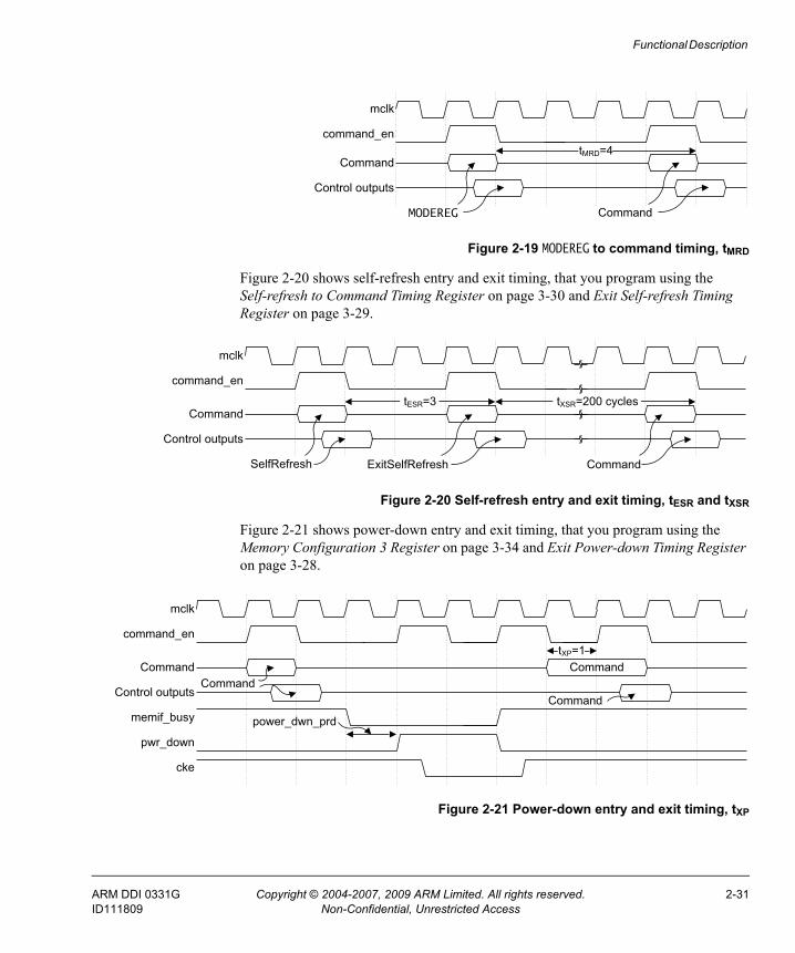
Functional Description
Figure 2-19 MODEREG to command timing, tMRD
Figure 2-20 shows self-refresh entry and exit timing, that you program using the Self-refresh to Command Timing Register on page 3-30 and Exit Self-refresh Timing Register on page 3-29.
Figure 2-20 Self-refresh entry and exit timing, tESR and tXSR
Figure 2-21 shows power-down entry and exit timing, that you program using the Memory Configuration 3 Register on page 3-34 and Exit Power-down Timing Register on page 3-28.
Figure 2-21 Power-down entry and exit timing, tXP
mclk
command_en
Command
Control outputs
tMRD=4
CommandMODEREG
mclk
command_en
Command
Control outputs
tXSR=200 cycles
ExitSelfRefresh
tESR=3
CommandSelfRefresh
tXP=1
mclk
command_en
Command
Control outputs
Command
CommandCommand
power_dwn_prd
pwr_down
cke
memif_busy
ARM DDI 0331G Copyright © 2004-2007, 2009 ARM Limited. All rights reserved. 2-31ID111809 Non-Confidential, Unrestricted Access
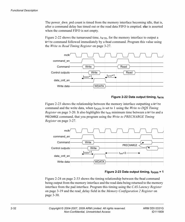
Functional Description
The power_dwn_prd count is timed from the memory interface becoming idle, that is, after a command delay has timed out or the read data FIFO is emptied. cke is asserted when the command FIFO is not empty.
Figure 2-22 shows the turnaround time, tWTR, for the memory interface to output a Write command followed immediately by a Read command. Program this value using the Write to Read Timing Register on page 3-27.
Figure 2-22 Data output timing, tWTR
Figure 2-23 shows the relationship between the memory interface outputting a Write command and the write data, when tDQSS is set to 1 using the Write to DQS Timing Register on page 3-20. It also highlights the tWR minimum time between a Write and a PRECHARGE command, that you program using the Write to PRECHARGE Timing Register on page 3-27.
Figure 2-23 Data output timing, tDQSS = 1
Figure 2-24 on page 2-33 shows the timing relationship between the Read command being output from the memory interface and the read data being returned to the memory interface from the pad interface. Program this timing using the CAS Latency Register on page 3-19 and the read_delay field in the Memory Configuration 2 Register on page 3-30.
mclk
command_en
Command
Control outputs
Write Read
Read
data_cntl_en
Write data WDATA
tWTR=1Write
tDQSS=1
mclk
command_en
Command
Control outputs
Write
data_cntl_en
Write data WDATA
tWR=3
WritePRECHARGE
tDQSS=1
2-32 Copyright © 2004-2007, 2009 ARM Limited. All rights reserved. ARM DDI 0331GNon-Confidential, Unrestricted Access ID111809
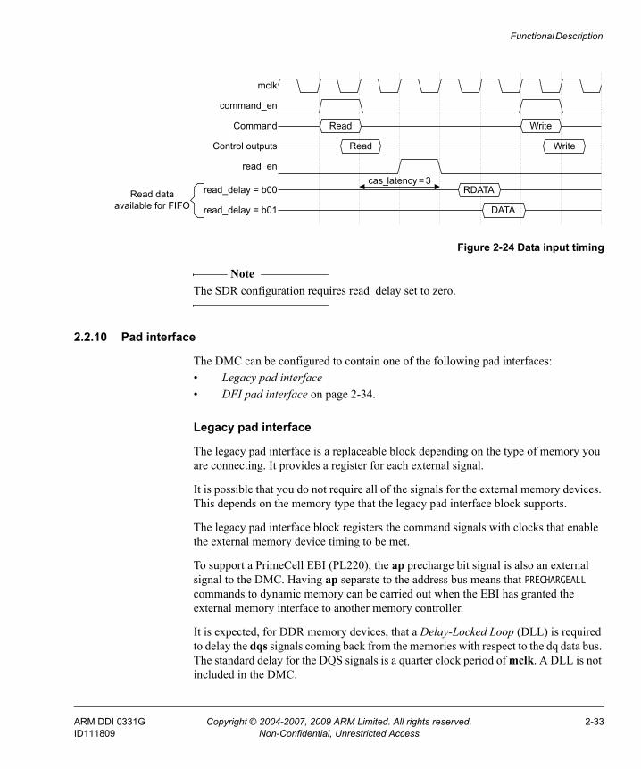
Functional Description
Figure 2-24 Data input timing
Note The SDR configuration requires read_delay set to zero.
2.2.10 Pad interface
The DMC can be configured to contain one of the following pad interfaces:• Legacy pad interface• DFI pad interface on page 2-34.
Legacy pad interface
The legacy pad interface is a replaceable block depending on the type of memory you are connecting. It provides a register for each external signal.
It is possible that you do not require all of the signals for the external memory devices. This depends on the memory type that the legacy pad interface block supports.
The legacy pad interface block registers the command signals with clocks that enable the external memory device timing to be met.
To support a PrimeCell EBI (PL220), the ap precharge bit signal is also an external signal to the DMC. Having ap separate to the address bus means that PRECHARGEALL commands to dynamic memory can be carried out when the EBI has granted the external memory interface to another memory controller.
It is expected, for DDR memory devices, that a Delay-Locked Loop (DLL) is required to delay the dqs signals coming back from the memories with respect to the dq data bus. The standard delay for the DQS signals is a quarter clock period of mclk. A DLL is not included in the DMC.
cas_latency = 3
mclk
command_en
Command
Control outputs
Read Write
Write
RDATA
Read
DATA
read_en
read_delay = b00
read_delay = b01Read data
available for FIFO
ARM DDI 0331G Copyright © 2004-2007, 2009 ARM Limited. All rights reserved. 2-33ID111809 Non-Confidential, Unrestricted Access
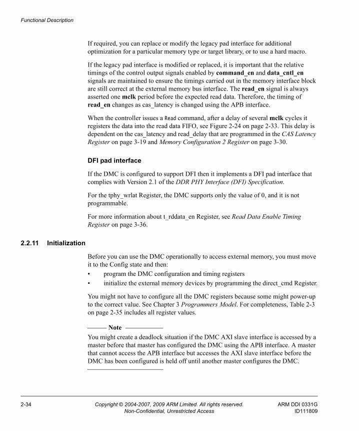
Functional Description
If required, you can replace or modify the legacy pad interface for additional optimization for a particular memory type or target library, or to use a hard macro.
If the legacy pad interface is modified or replaced, it is important that the relative timings of the control output signals enabled by command_en and data_cntl_en signals are maintained to ensure the timings carried out in the memory interface block are still correct at the external memory bus interface. The read_en signal is always asserted one mclk period before the expected read data. Therefore, the timing of read_en changes as cas_latency is changed using the APB interface.
When the controller issues a Read command, after a delay of several mclk cycles it registers the data into the read data FIFO, see Figure 2-24 on page 2-33. This delay is dependent on the cas_latency and read_delay that are programmed in the CAS Latency Register on page 3-19 and Memory Configuration 2 Register on page 3-30.
DFI pad interface
If the DMC is configured to support DFI then it implements a DFI pad interface that complies with Version 2.1 of the DDR PHY Interface (DFI) Specification.
For the tphy_wrlat Register, the DMC supports only the value of 0, and it is not programmable.
For more information about t_rddata_en Register, see Read Data Enable Timing Register on page 3-36.
2.2.11 Initialization
Before you can use the DMC operationally to access external memory, you must move it to the Config state and then:• program the DMC configuration and timing registers• initialize the external memory devices by programming the direct_cmd Register.
You might not have to configure all the DMC registers because some might power-up to the correct value. See Chapter 3 Programmers Model. For completeness, Table 2-3 on page 2-35 includes all register values.
Note You might create a deadlock situation if the DMC AXI slave interface is accessed by a master before that master has configured the DMC using the APB interface. A master that cannot access the APB interface but accesses the AXI slave interface before the DMC has been configured is held off until another master configures the DMC.
2-34 Copyright © 2004-2007, 2009 ARM Limited. All rights reserved. ARM DDI 0331GNon-Confidential, Unrestricted Access ID111809
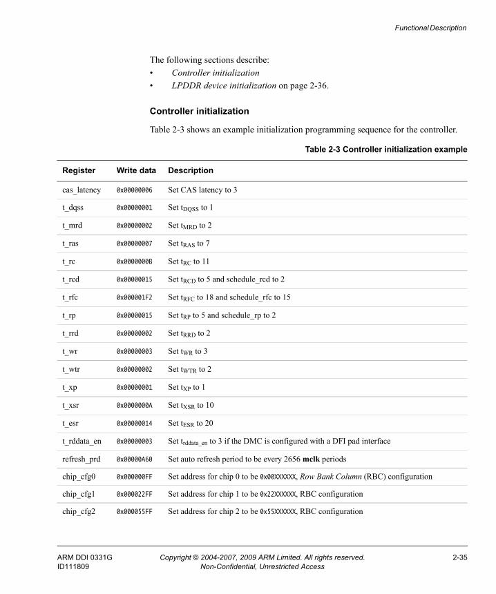
Functional Description
The following sections describe:• Controller initialization• LPDDR device initialization on page 2-36.
Controller initialization
Table 2-3 shows an example initialization programming sequence for the controller.
Table 2-3 Controller initialization example
Register Write data Description
cas_latency 0x00000006 Set CAS latency to 3
t_dqss 0x00000001 Set tDQSS to 1
t_mrd 0x00000002 Set tMRD to 2
t_ras 0x00000007 Set tRAS to 7
t_rc 0x0000000B Set tRC to 11
t_rcd 0x00000015 Set tRCD to 5 and schedule_rcd to 2
t_rfc 0x000001F2 Set tRFC to 18 and schedule_rfc to 15
t_rp 0x00000015 Set tRP to 5 and schedule_rp to 2
t_rrd 0x00000002 Set tRRD to 2
t_wr 0x00000003 Set tWR to 3
t_wtr 0x00000002 Set tWTR to 2
t_xp 0x00000001 Set tXP to 1
t_xsr 0x0000000A Set tXSR to 10
t_esr 0x00000014 Set tESR to 20
t_rddata_en 0x00000003 Set trddata_en to 3 if the DMC is configured with a DFI pad interface
refresh_prd 0x00000A60 Set auto refresh period to be every 2656 mclk periods
chip_cfg0 0x000000FF Set address for chip 0 to be 0x00XXXXXX, Row Bank Column (RBC) configuration
chip_cfg1 0x000022FF Set address for chip 1 to be 0x22XXXXXX, RBC configuration
chip_cfg2 0x000055FF Set address for chip 2 to be 0x55XXXXXX, RBC configuration
ARM DDI 0331G Copyright © 2004-2007, 2009 ARM Limited. All rights reserved. 2-35ID111809 Non-Confidential, Unrestricted Access
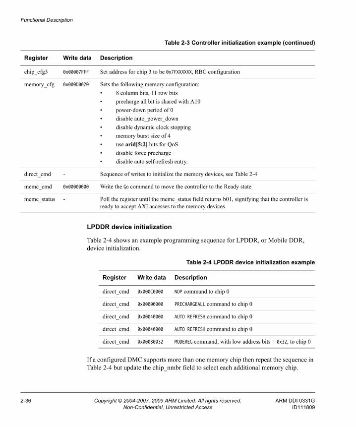
Functional Description
LPDDR device initialization
Table 2-4 shows an example programming sequence for LPDDR, or Mobile DDR, device initialization.
If a configured DMC supports more than one memory chip then repeat the sequence in Table 2-4 but update the chip_nmbr field to select each additional memory chip.
chip_cfg3 0x00007FFF Set address for chip 3 to be 0x7FXXXXXX, RBC configuration
memory_cfg 0x000D0020 Sets the following memory configuration:• 8 column bits, 11 row bits• precharge all bit is shared with A10• power-down period of 0• disable auto_power_down• disable dynamic clock stopping• memory burst size of 4• use arid[5:2] bits for QoS• disable force precharge• disable auto self-refresh entry.
direct_cmd - Sequence of writes to initialize the memory devices, see Table 2-4
memc_cmd 0x00000000 Write the Go command to move the controller to the Ready state
memc_status - Poll the register until the memc_status field returns b01, signifying that the controller is ready to accept AXI accesses to the memory devices
Table 2-3 Controller initialization example (continued)
Register Write data Description
Table 2-4 LPDDR device initialization example
Register Write data Description
direct_cmd 0x000C0000 NOP command to chip 0
direct_cmd 0x00000000 PRECHARGEALL command to chip 0
direct_cmd 0x00040000 AUTO REFRESH command to chip 0
direct_cmd 0x00040000 AUTO REFRESH command to chip 0
direct_cmd 0x00080032 MODEREG command, with low address bits = 0x32, to chip 0
2-36 Copyright © 2004-2007, 2009 ARM Limited. All rights reserved. ARM DDI 0331GNon-Confidential, Unrestricted Access ID111809
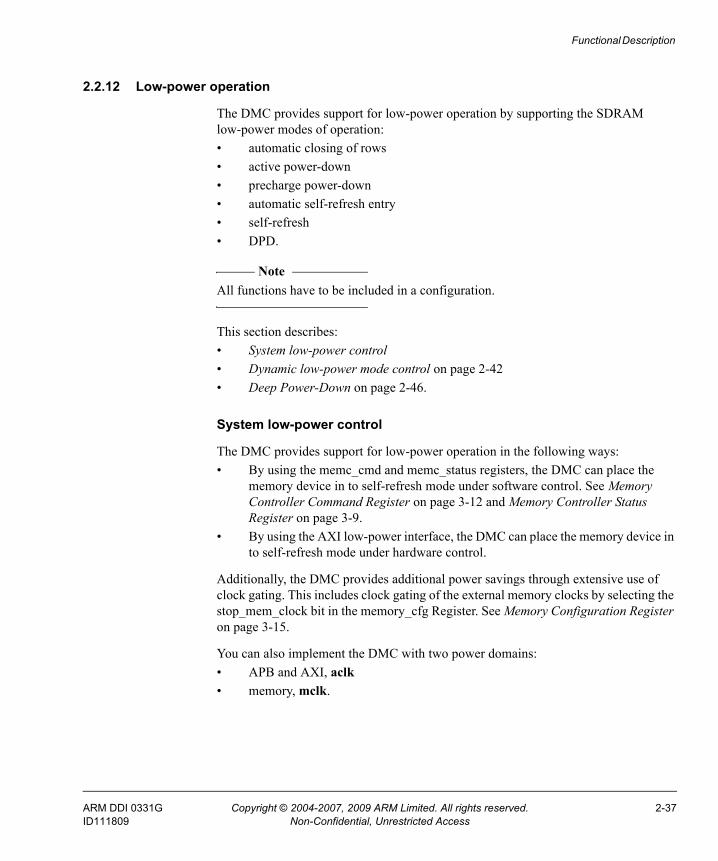
Functional Description
2.2.12 Low-power operation
The DMC provides support for low-power operation by supporting the SDRAM low-power modes of operation:• automatic closing of rows• active power-down• precharge power-down• automatic self-refresh entry• self-refresh• DPD.
Note All functions have to be included in a configuration.
This section describes:• System low-power control• Dynamic low-power mode control on page 2-42• Deep Power-Down on page 2-46.
System low-power control
The DMC provides support for low-power operation in the following ways:• By using the memc_cmd and memc_status registers, the DMC can place the
memory device in to self-refresh mode under software control. See Memory Controller Command Register on page 3-12 and Memory Controller Status Register on page 3-9.
• By using the AXI low-power interface, the DMC can place the memory device in to self-refresh mode under hardware control.
Additionally, the DMC provides additional power savings through extensive use of clock gating. This includes clock gating of the external memory clocks by selecting the stop_mem_clock bit in the memory_cfg Register. See Memory Configuration Register on page 3-15.
You can also implement the DMC with two power domains:• APB and AXI, aclk• memory, mclk.
ARM DDI 0331G Copyright © 2004-2007, 2009 ARM Limited. All rights reserved. 2-37ID111809 Non-Confidential, Unrestricted Access
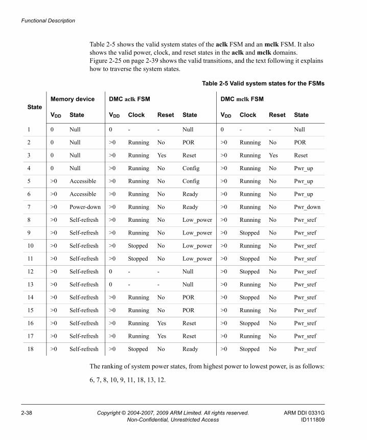
Functional Description
Table 2-5 shows the valid system states of the aclk FSM and an mclk FSM. It also shows the valid power, clock, and reset states in the aclk and mclk domains. Figure 2-25 on page 2-39 shows the valid transitions, and the text following it explains how to traverse the system states.
The ranking of system power states, from highest power to lowest power, is as follows:
6, 7, 8, 10, 9, 11, 18, 13, 12.
Table 2-5 Valid system states for the FSMs
StateMemory device DMC aclk FSM DMC mclk FSM
VDD State VDD Clock Reset State VDD Clock Reset State
1 0 Null 0 - - Null 0 - - Null
2 0 Null >0 Running No POR >0 Running No POR
3 0 Null >0 Running Yes Reset >0 Running Yes Reset
4 0 Null >0 Running No Config >0 Running No Pwr_up
5 >0 Accessible >0 Running No Config >0 Running No Pwr_up
6 >0 Accessible >0 Running No Ready >0 Running No Pwr_up
7 >0 Power-down >0 Running No Ready >0 Running No Pwr_down
8 >0 Self-refresh >0 Running No Low_power >0 Running No Pwr_sref
9 >0 Self-refresh >0 Running No Low_power >0 Stopped No Pwr_sref
10 >0 Self-refresh >0 Stopped No Low_power >0 Running No Pwr_sref
11 >0 Self-refresh >0 Stopped No Low_power >0 Stopped No Pwr_sref
12 >0 Self-refresh 0 - - Null >0 Stopped No Pwr_sref
13 >0 Self-refresh 0 - - Null >0 Running No Pwr_sref
14 >0 Self-refresh >0 Running No POR >0 Stopped No Pwr_sref
15 >0 Self-refresh >0 Running No POR >0 Running No Pwr_sref
16 >0 Self-refresh >0 Running Yes Reset >0 Stopped No Pwr_sref
17 >0 Self-refresh >0 Running Yes Reset >0 Running No Pwr_sref
18 >0 Self-refresh >0 Stopped No Ready >0 Stopped No Pwr_sref
2-38 Copyright © 2004-2007, 2009 ARM Limited. All rights reserved. ARM DDI 0331GNon-Confidential, Unrestricted Access ID111809
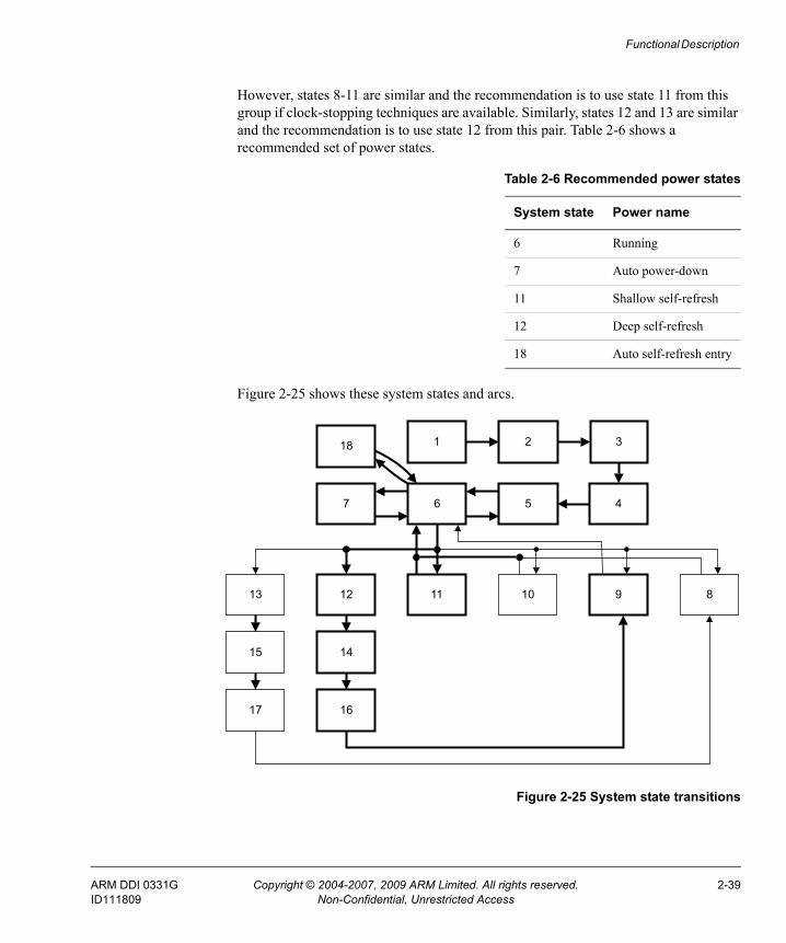
Functional Description
However, states 8-11 are similar and the recommendation is to use state 11 from this group if clock-stopping techniques are available. Similarly, states 12 and 13 are similar and the recommendation is to use state 12 from this pair. Table 2-6 shows a recommended set of power states.
Figure 2-25 shows these system states and arcs.
Figure 2-25 System state transitions
Table 2-6 Recommended power states
System state Power name
6 Running
7 Auto power-down
11 Shallow self-refresh
12 Deep self-refresh
18 Auto self-refresh entry
1 2 3
4567
111213
1415
1617
10 9 8
18
ARM DDI 0331G Copyright © 2004-2007, 2009 ARM Limited. All rights reserved. 2-39ID111809 Non-Confidential, Unrestricted Access
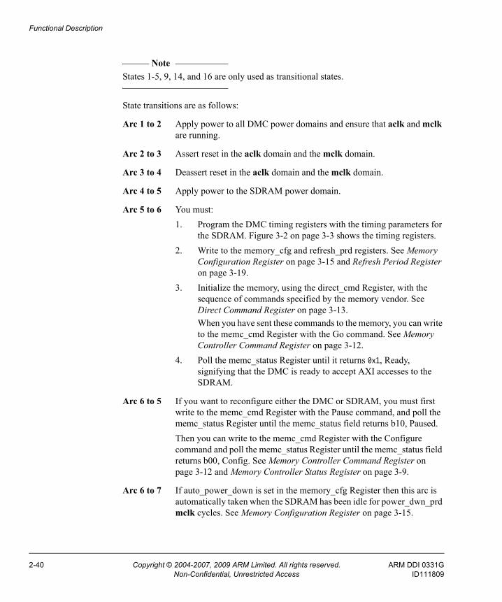
Functional Description
Note States 1-5, 9, 14, and 16 are only used as transitional states.
State transitions are as follows:
Arc 1 to 2 Apply power to all DMC power domains and ensure that aclk and mclk are running.
Arc 2 to 3 Assert reset in the aclk domain and the mclk domain.
Arc 3 to 4 Deassert reset in the aclk domain and the mclk domain.
Arc 4 to 5 Apply power to the SDRAM power domain.
Arc 5 to 6 You must:1. Program the DMC timing registers with the timing parameters for
the SDRAM. Figure 3-2 on page 3-3 shows the timing registers.2. Write to the memory_cfg and refresh_prd registers. See Memory
Configuration Register on page 3-15 and Refresh Period Register on page 3-19.
3. Initialize the memory, using the direct_cmd Register, with the sequence of commands specified by the memory vendor. See Direct Command Register on page 3-13.When you have sent these commands to the memory, you can write to the memc_cmd Register with the Go command. See Memory Controller Command Register on page 3-12.
4. Poll the memc_status Register until it returns 0x1, Ready, signifying that the DMC is ready to accept AXI accesses to the SDRAM.
Arc 6 to 5 If you want to reconfigure either the DMC or SDRAM, you must first write to the memc_cmd Register with the Pause command, and poll the memc_status Register until the memc_status field returns b10, Paused.Then you can write to the memc_cmd Register with the Configure command and poll the memc_status Register until the memc_status field returns b00, Config. See Memory Controller Command Register on page 3-12 and Memory Controller Status Register on page 3-9.
Arc 6 to 7 If auto_power_down is set in the memory_cfg Register then this arc is automatically taken when the SDRAM has been idle for power_dwn_prd mclk cycles. See Memory Configuration Register on page 3-15.
2-40 Copyright © 2004-2007, 2009 ARM Limited. All rights reserved. ARM DDI 0331GNon-Confidential, Unrestricted Access ID111809
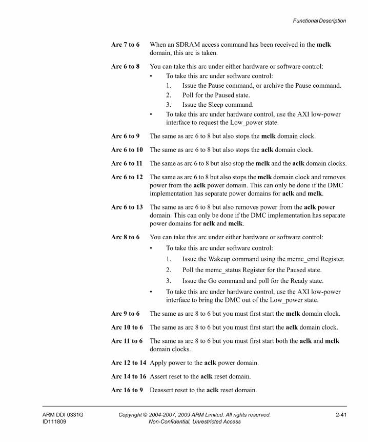
Functional Description
Arc 7 to 6 When an SDRAM access command has been received in the mclk domain, this arc is taken.
Arc 6 to 8 You can take this arc under either hardware or software control:• To take this arc under software control:
1. Issue the Pause command, or archive the Pause command.2. Poll for the Paused state.3. Issue the Sleep command.
• To take this arc under hardware control, use the AXI low-power interface to request the Low_power state.
Arc 6 to 9 The same as arc 6 to 8 but also stops the mclk domain clock.
Arc 6 to 10 The same as arc 6 to 8 but also stops the aclk domain clock.
Arc 6 to 11 The same as arc 6 to 8 but also stop the mclk and the aclk domain clocks.
Arc 6 to 12 The same as arc 6 to 8 but also stops the mclk domain clock and removes power from the aclk power domain. This can only be done if the DMC implementation has separate power domains for aclk and mclk.
Arc 6 to 13 The same as arc 6 to 8 but also removes power from the aclk power domain. This can only be done if the DMC implementation has separate power domains for aclk and mclk.
Arc 8 to 6 You can take this arc under either hardware or software control:• To take this arc under software control:
1. Issue the Wakeup command using the memc_cmd Register.2. Poll the memc_status Register for the Paused state.3. Issue the Go command and poll for the Ready state.
• To take this arc under hardware control, use the AXI low-power interface to bring the DMC out of the Low_power state.
Arc 9 to 6 The same as arc 8 to 6 but you must first start the mclk domain clock.
Arc 10 to 6 The same as arc 8 to 6 but you must first start the aclk domain clock.
Arc 11 to 6 The same as arc 8 to 6 but you must first start both the aclk and mclk domain clocks.
Arc 12 to 14 Apply power to the aclk power domain.
Arc 14 to 16 Assert reset to the aclk reset domain.
Arc 16 to 9 Deassert reset to the aclk reset domain.
ARM DDI 0331G Copyright © 2004-2007, 2009 ARM Limited. All rights reserved. 2-41ID111809 Non-Confidential, Unrestricted Access
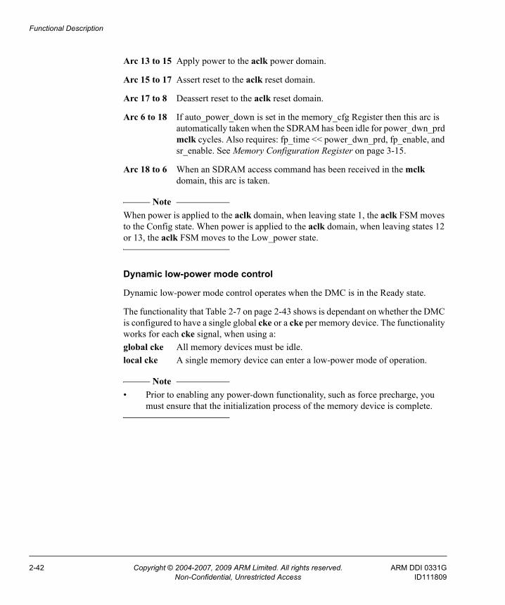
Functional Description
Arc 13 to 15 Apply power to the aclk power domain.
Arc 15 to 17 Assert reset to the aclk reset domain.
Arc 17 to 8 Deassert reset to the aclk reset domain.
Arc 6 to 18 If auto_power_down is set in the memory_cfg Register then this arc is automatically taken when the SDRAM has been idle for power_dwn_prd mclk cycles. Also requires: fp_time << power_dwn_prd, fp_enable, and sr_enable. See Memory Configuration Register on page 3-15.
Arc 18 to 6 When an SDRAM access command has been received in the mclk domain, this arc is taken.
Note When power is applied to the aclk domain, when leaving state 1, the aclk FSM moves to the Config state. When power is applied to the aclk domain, when leaving states 12 or 13, the aclk FSM moves to the Low_power state.
Dynamic low-power mode control
Dynamic low-power mode control operates when the DMC is in the Ready state.
The functionality that Table 2-7 on page 2-43 shows is dependant on whether the DMC is configured to have a single global cke or a cke per memory device. The functionality works for each cke signal, when using a:global cke All memory devices must be idle.local cke A single memory device can enter a low-power mode of operation.
Note • Prior to enabling any power-down functionality, such as force precharge, you
must ensure that the initialization process of the memory device is complete.
2-42 Copyright © 2004-2007, 2009 ARM Limited. All rights reserved. ARM DDI 0331GNon-Confidential, Unrestricted Access ID111809
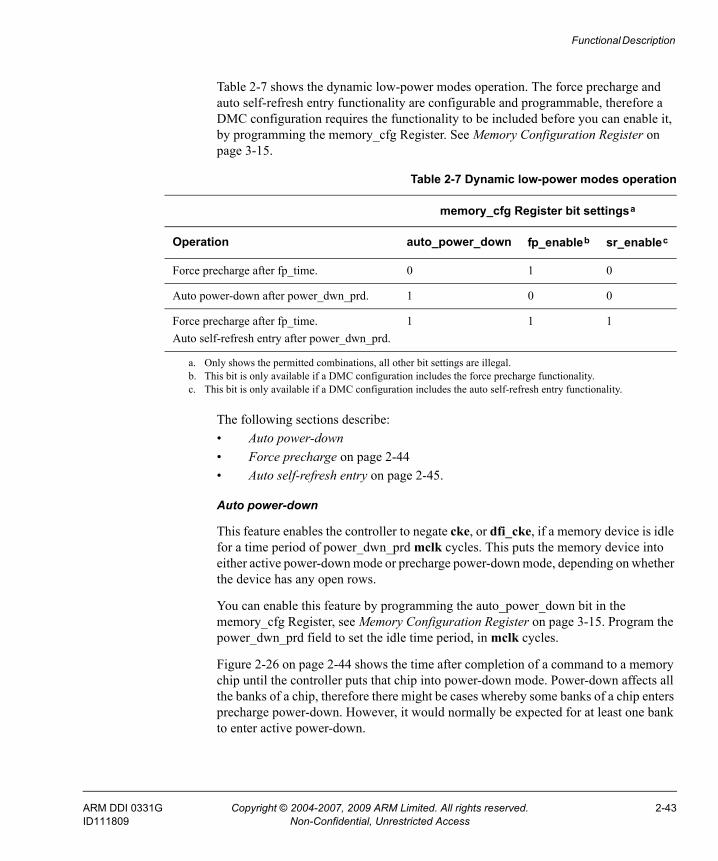
Functional Description
Table 2-7 shows the dynamic low-power modes operation. The force precharge and auto self-refresh entry functionality are configurable and programmable, therefore a DMC configuration requires the functionality to be included before you can enable it, by programming the memory_cfg Register. See Memory Configuration Register on page 3-15.
The following sections describe:• Auto power-down• Force precharge on page 2-44• Auto self-refresh entry on page 2-45.
Auto power-down
This feature enables the controller to negate cke, or dfi_cke, if a memory device is idle for a time period of power_dwn_prd mclk cycles. This puts the memory device into either active power-down mode or precharge power-down mode, depending on whether the device has any open rows.
You can enable this feature by programming the auto_power_down bit in the memory_cfg Register, see Memory Configuration Register on page 3-15. Program the power_dwn_prd field to set the idle time period, in mclk cycles.
Figure 2-26 on page 2-44 shows the time after completion of a command to a memory chip until the controller puts that chip into power-down mode. Power-down affects all the banks of a chip, therefore there might be cases whereby some banks of a chip enters precharge power-down. However, it would normally be expected for at least one bank to enter active power-down.
Table 2-7 Dynamic low-power modes operation
memory_cfg Register bit settingsa
Operation auto_power_down fp_enableb sr_enablec
Force precharge after fp_time. 0 1 0
Auto power-down after power_dwn_prd. 1 0 0
Force precharge after fp_time.Auto self-refresh entry after power_dwn_prd.
1 1 1
a. Only shows the permitted combinations, all other bit settings are illegal.b. This bit is only available if a DMC configuration includes the force precharge functionality.c. This bit is only available if a DMC configuration includes the auto self-refresh entry functionality.
ARM DDI 0331G Copyright © 2004-2007, 2009 ARM Limited. All rights reserved. 2-43ID111809 Non-Confidential, Unrestricted Access
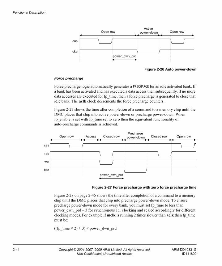
Functional Description
Figure 2-26 Auto power-down
Force precharge
Force precharge logic automatically generates a PRECHARGE for an idle activated bank. If a bank has been activated and has executed a data access then subsequently, if no more data accesses are executed for fp_time, then a force precharge is generated to close that idle bank. The aclk clock decrements the force precharge counters.
Figure 2-27 shows the time after completion of a command to a memory chip until the DMC places that chip into active power-down or precharge power-down. When fp_enable is set with fp_time set to zero then the equivalent functionality of auto-precharge commands is achieved.
Figure 2-27 Force precharge with zero force precharge time
Figure 2-28 on page 2-45 shows the time after completion of a command to a memory chip until the DMC places that chip into precharge power-down mode. To ensure precharge power-down mode for every bank, you must set fp_time to less than power_dwn_prd – 3 for synchronous 1:1 clocking and scaled accordingly for different clocking modes. For example if mclk is running 2 times slower than aclk then fp_time must be:
((fp_time × 2) + 3) < power_dwn_prd
cas
ckepower_dwn_prd
Active power-downOpen row Open row
cas
ckepower_dwn_prd
Precharge power-downOpen row Open row
ras
we
Closed row Closed rowAccess
2-44 Copyright © 2004-2007, 2009 ARM Limited. All rights reserved. ARM DDI 0331GNon-Confidential, Unrestricted Access ID111809
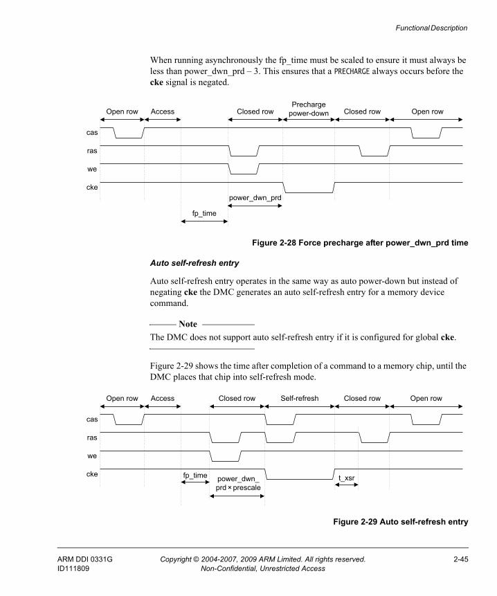
Functional Description
When running asynchronously the fp_time must be scaled to ensure it must always be less than power_dwn_prd – 3. This ensures that a PRECHARGE always occurs before the cke signal is negated.
Figure 2-28 Force precharge after power_dwn_prd time
Auto self-refresh entry
Auto self-refresh entry operates in the same way as auto power-down but instead of negating cke the DMC generates an auto self-refresh entry for a memory device command.
Note The DMC does not support auto self-refresh entry if it is configured for global cke.
Figure 2-29 shows the time after completion of a command to a memory chip, until the DMC places that chip into self-refresh mode.
Figure 2-29 Auto self-refresh entry
cas
ckepower_dwn_prd
Precharge power-downOpen row Open row
ras
we
Closed row Closed rowAccess
fp_time
cas
cke
Self-refreshOpen row Open row
ras
we
Closed row Closed rowAccess
t_xsrfp_time power_dwn_prd × prescale
ARM DDI 0331G Copyright © 2004-2007, 2009 ARM Limited. All rights reserved. 2-45ID111809 Non-Confidential, Unrestricted Access
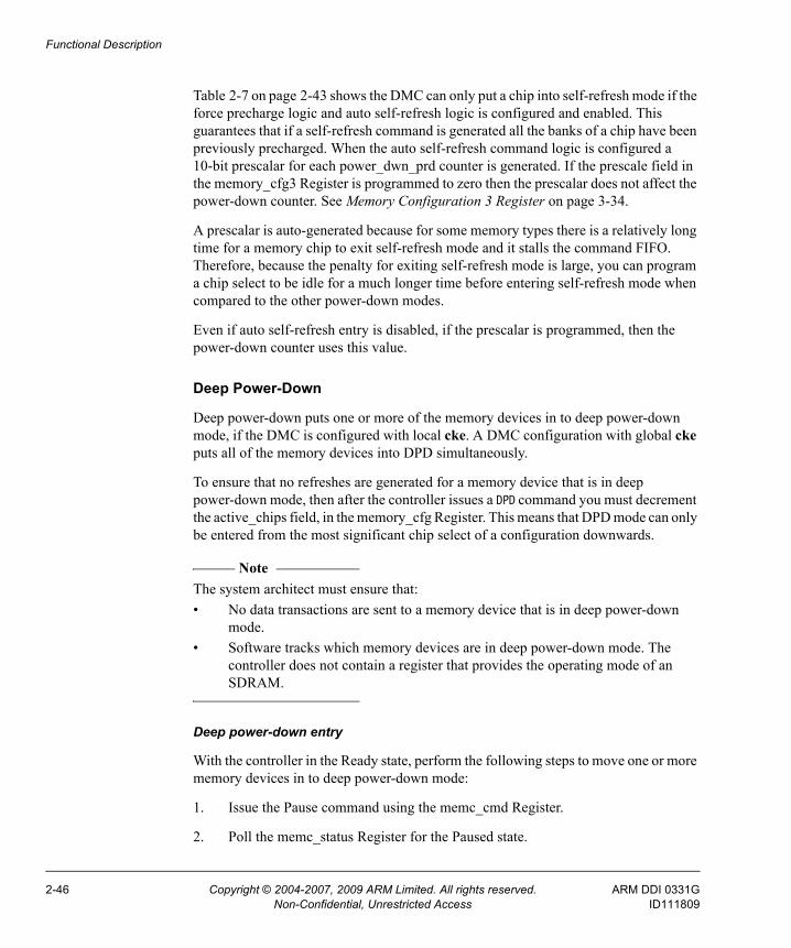
Functional Description
Table 2-7 on page 2-43 shows the DMC can only put a chip into self-refresh mode if the force precharge logic and auto self-refresh logic is configured and enabled. This guarantees that if a self-refresh command is generated all the banks of a chip have been previously precharged. When the auto self-refresh command logic is configured a 10-bit prescalar for each power_dwn_prd counter is generated. If the prescale field in the memory_cfg3 Register is programmed to zero then the prescalar does not affect the power-down counter. See Memory Configuration 3 Register on page 3-34.
A prescalar is auto-generated because for some memory types there is a relatively long time for a memory chip to exit self-refresh mode and it stalls the command FIFO. Therefore, because the penalty for exiting self-refresh mode is large, you can program a chip select to be idle for a much longer time before entering self-refresh mode when compared to the other power-down modes.
Even if auto self-refresh entry is disabled, if the prescalar is programmed, then the power-down counter uses this value.
Deep Power-Down
Deep power-down puts one or more of the memory devices in to deep power-down mode, if the DMC is configured with local cke. A DMC configuration with global cke puts all of the memory devices into DPD simultaneously.
To ensure that no refreshes are generated for a memory device that is in deep power-down mode, then after the controller issues a DPD command you must decrement the active_chips field, in the memory_cfg Register. This means that DPD mode can only be entered from the most significant chip select of a configuration downwards.
Note The system architect must ensure that:• No data transactions are sent to a memory device that is in deep power-down
mode.• Software tracks which memory devices are in deep power-down mode. The
controller does not contain a register that provides the operating mode of an SDRAM.
Deep power-down entry
With the controller in the Ready state, perform the following steps to move one or more memory devices in to deep power-down mode:
1. Issue the Pause command using the memc_cmd Register.
2. Poll the memc_status Register for the Paused state.
2-46 Copyright © 2004-2007, 2009 ARM Limited. All rights reserved. ARM DDI 0331GNon-Confidential, Unrestricted Access ID111809
Functional Description
3. Issue the Config command using the memc_cmd Register.
4. Poll the memc_status Register for the Config state.
5. Write to the direct_cmd Register with the PRECHARGEALL command. Program the chip_nmbr field to be the highest chip select that is active.
6. Write to the direct_cmd Register with the DPD command and set the chip_nmbr field to the value from step 5. The chip_nmbr field selects which SDRAM enters deep power-down mode.
Note If the controller is configured with global cke then the controller moves all the
SDRAMs to deep power-down mode, irrespective of the chip_nmbr field value. The controller must then remain in Config state until the memory devices are removed from deep power-down mode.
7. If the controller is configured with local cke then repeat steps 5 and 6 if you require other SDRAMs to enter deep power-down mode.
8. Write to the active_chips field of the memory_cfg Register to disable refreshes for SDRAMs that are in deep power-down mode. See Memory Configuration Register on page 3-15.
Note If all the SDRAMs are in deep power-down mode then the controller must remain in Config state until one of the memory devices is removed from deep power-down mode.
Deep power-down exit
With the controller in the Ready state, perform the following steps to remove one or more memory devices from deep power-down mode:
Note If all of the memory devices are in deep power-down mode then the controller must be in the Config state and you can ignore steps 1-4.
1. Issue the Pause command using the memc_cmd Register.
2. Poll the memc_status Register for the Paused state.
3. Issue the Config command using the memc_cmd Register.
4. Poll the memc_status Register for the Config state.
ARM DDI 0331G Copyright © 2004-2007, 2009 ARM Limited. All rights reserved. 2-47ID111809 Non-Confidential, Unrestricted Access
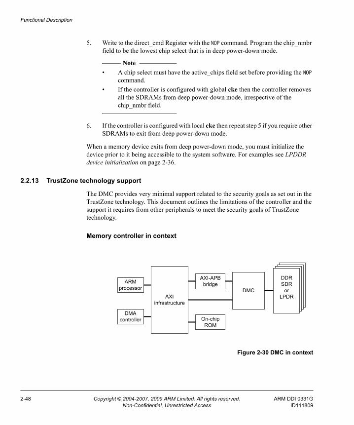
Functional Description
5. Write to the direct_cmd Register with the NOP command. Program the chip_nmbr field to be the lowest chip select that is in deep power-down mode.
Note • A chip select must have the active_chips field set before providing the NOP
command.• If the controller is configured with global cke then the controller removes
all the SDRAMs from deep power-down mode, irrespective of the chip_nmbr field.
6. If the controller is configured with local cke then repeat step 5 if you require other SDRAMs to exit from deep power-down mode.
When a memory device exits from deep power-down mode, you must initialize the device prior to it being accessible to the system software. For examples see LPDDR device initialization on page 2-36.
2.2.13 TrustZone technology support
The DMC provides very minimal support related to the security goals as set out in the TrustZone technology. This document outlines the limitations of the controller and the support it requires from other peripherals to meet the security goals of TrustZone technology.
Memory controller in context
Figure 2-30 DMC in context
AXI-APB bridge
AXI infrastructure
ARM processor
DMAcontroller On-chip
ROM
DDR SDR
orLPDR
DMC
2-48 Copyright © 2004-2007, 2009 ARM Limited. All rights reserved. ARM DDI 0331GNon-Confidential, Unrestricted Access ID111809
Functional Description
The DMC has an AXI slave interface and an APB interface. The APB interface has to be placed in a location which is only addressable by the Secure world. The AXI slave interface can be addressed by both the Secure and Non-secure world.
The DMC does not distinguish between secure read or write data transactions and non-secure access on its AXI or APB interfaces.
There are 3 possible security configurations that need to be considered.
Note Secure memory and non-secure memory only refer to access control of memory locations as set out in the TrustZone technology.
Non-secure memory All memory locations addressed through the DMC are not protected by TrustZone technology and they are accessible to either the Secure or Non-secure worlds. The AXI and APB interfaces of the DMC are mapped to be accessible by the Secure and Non-secure worlds.
Dedicated secure memory All memory locations addressed through the DMC are always protected by TrustZone technology and are accessible only to the Secure world. The AXI and APB regions that connect to the DMC must be mapped as secure.
Shared secure and non-secure memory Memory locations addressed through the DMC contains both secure and non-secure memory regions. An AXI bridging device is required to meet the security goals of TrustZone technology.
APB interface
When any of the regions addressed by an DMC are made secure on the AXI slave interface, then the control of the mapping of the memories at the DMC has to be made equally secure by ensuring that only the Secure world can access the APB interface.
AXI slave interface
The DMC does not distinguish between Secure and Non-secure world access to the AXI slave interface. Memory transactions are not aborted. It does not make the read data as null when a non-secure read request tries to access a secure memory region. Write
ARM DDI 0331G Copyright © 2004-2007, 2009 ARM Limited. All rights reserved. 2-49ID111809 Non-Confidential, Unrestricted Access
Functional Description
strobes are not disabled when a non-secure write request tries to access a secure memory region. Therefore the AXI slave interface has to be access controlled to meet the security goals of TrustZone technology.
Memory regions
The DMC can support a maximum of four chip-selects (memory devices). It supports 32-bits of AXI address bus. Hence it can access up to 4 GBytes of data. This memory range can be divided into multiple memory regions up to a maximum of four. This is defined by individual chip_<n>_cfg registers that are programmable through the APB interface. Each of the individual chip_<n>_cfg registers has an address match field and an address mask field.
Chip configuration register map
Chip configuration Register can only be read or written in the Config or Low_power states. See Chip Configuration Register on page 3-39.
It is possible to define overlapping memory regions. This can result in two different AXI addresses mapping to the same memory region. Therefore overlapping memory regions must not be defined and control of the mapping of the memories at the DMC must be made secure by ensuring that only the Secure world can access the APB interface.
If the DMC receives an AXI access that does not map to a chip select then the controller performs the access to chip select 0. If the memory device that connects to chip select 0 contains secure data then it is possible for a master in Non-secure state to access that data. To prevent this security violation from occurring, you must ensure that the interconnect or system that connects to the controller, can only issue accesses that map directly to a chip select.
Side-channel interface (clock, reset, and power)
The programmable voltage and frequency sources inside a system must stay within specification, so the device that controls the voltage and frequency must be secured by TrustZone access control techniques.
Caution
TrustZone security extensions enables a secure software environment. The technology does not protect the processor, DMC, or other peripherals from hardware attacks and the implementer must take appropriate steps to secure the hardware and protect the trusted code.
2-50 Copyright © 2004-2007, 2009 ARM Limited. All rights reserved. ARM DDI 0331GNon-Confidential, Unrestricted Access ID111809
Chapter 3 Programmers Model
This chapter describes the DMC registers and provides information for programming the device. It contains the following sections:• About the programmers model on page 3-2• Register summary on page 3-6• Register descriptions on page 3-9.
ARM DDI 0331G Copyright © 2004-2007, 2009 ARM Limited. All rights reserved. 3-1ID111809 Non-Confidential, Unrestricted Access
Programmers Model
3.1 About the programmers modelThe following information applies to the DMC registers:• The base address is not fixed, and can be different for any particular system
implementation. The offset of each register from the base address is fixed.• Do not attempt to access reserved or unused address locations. Attempting to
access these location can result in Unpredictable behavior.• Unless otherwise stated in the accompanying text:
— do not modify undefined register bits— ignore undefined register bits on reads— all register bits are reset to a logic 0 by a system or power-on reset.
• Access type in Register summary on page 3-6 is described as follows:RW Read and write.RO Read only.WO Write only.
3.1.1 Register map
The register map of the DMC spans a 4KB region, see Figure 3-1.
Figure 3-1 Register map
In Figure 3-1 the register map consists of the following main blocks:• DMC configuration on page 3-3• AXI ID configuration on page 3-4
DMC configuration0x000
AXI ID configuration
Chip configuration
Integration test
Component configuration
0x100
0x200
0xE00
0xFE0
0xFFC
User-defined signals0x300
3-2 Copyright © 2004-2007, 2009 ARM Limited. All rights reserved. ARM DDI 0331GNon-Confidential, Unrestricted Access ID111809
Programmers Model
• Chip configuration on page 3-4• User configuration and Feature Control Register on page 3-4• Integration test on page 3-5• Component configuration on page 3-5.
DMC configuration
Figure 3-2 shows the DMC configuration register map.
Figure 3-2 DMC configuration register map
memc_status0x000
0x004memc_cmd
direct_cmd
memory_cfg
refresh_prd
cas_latency
t_dqss
t_mrd
t_ras
t_rc
t_rcd
t_rfc
t_rp
t_rrd
t_wr
t_wtr
t_xp
t_xsr
t_esr
0x008
0x00C
0x010
0x014
0x01C
0x018
0x024
0x020
0x028
0x02C
0x034
0x030
0x03C
0x038
0x044
0x040
0x048
0x04C
0x050memory_cfg2
memory_cfg30x054
0x058
t_rddata_en
update_type0x05C
Reserved
Timing registers
Timing registers
read_transfer_delay0x07C
ARM DDI 0331G Copyright © 2004-2007, 2009 ARM Limited. All rights reserved. 3-3ID111809 Non-Confidential, Unrestricted Access
Programmers Model
AXI ID configuration
Figure 3-3 shows the AXI ID configuration register map.
Figure 3-3 AXI ID configuration register map
Chip configuration
Figure 3-4 shows the chip configuration register map.
Figure 3-4 Chip configuration register map
User configuration and Feature Control Register
Figure 3-5 shows the memory map for the Feature Control Register and the following user signals:• user_config1[]• user_config0[]• user_status[].
Figure 3-5 User configuration register map
id_0_cfg0x100
0x104id_1_cfg
...
id_15_cfg0x13C
chip_cfg00x200
0x204chip_cfg1
chip_cfg3
0x208chip_cfg2
0x20C
user_config
user_status0x304
0x300
user_config10x308
feature_ctrl0x30C
3-4 Copyright © 2004-2007, 2009 ARM Limited. All rights reserved. ARM DDI 0331GNon-Confidential, Unrestricted Access ID111809
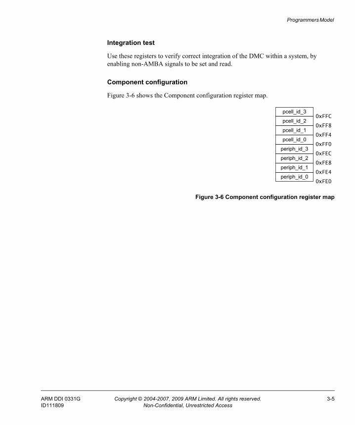
Programmers Model
Integration test
Use these registers to verify correct integration of the DMC within a system, by enabling non-AMBA signals to be set and read.
Component configuration
Figure 3-6 shows the Component configuration register map.
Figure 3-6 Component configuration register map
periph_id_00xFE0
0xFE4periph_id_1
pcell_id_00xFF0
periph_id_2
periph_id_3
pcell_id_1
pcell_id_2
pcell_id_3
0xFE8
0xFEC
0xFF4
0xFF8
0xFFC
ARM DDI 0331G Copyright © 2004-2007, 2009 ARM Limited. All rights reserved. 3-5ID111809 Non-Confidential, Unrestricted Access
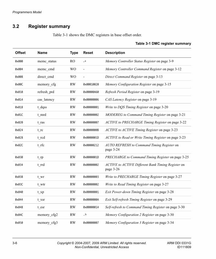
Programmers Model
3.2 Register summaryTable 3-1 shows the DMC registers in base offset order.
Table 3-1 DMC register summary
Offset Name Type Reset Description
0x000 memc_status RO -a Memory Controller Status Register on page 3-9
0x004 memc_cmd WO - Memory Controller Command Register on page 3-12
0x008 direct_cmd WO - Direct Command Register on page 3-13
0x00C memory_cfg RW 0x00010020 Memory Configuration Register on page 3-15
0x010 refresh_prd RW 0x00000A60 Refresh Period Register on page 3-19
0x014 cas_latency RW 0x00000006 CAS Latency Register on page 3-19
0x018 t_dqss RW 0x00000001 Write to DQS Timing Register on page 3-20
0x01C t_mrd RW 0x00000002 MODEREG to Command Timing Register on page 3-21
0x020 t_ras RW 0x00000007 ACTIVE to PRECHARGE Timing Register on page 3-22
0x024 t_rc RW 0x0000000B ACTIVE to ACTIVE Timing Register on page 3-23
0x028 t_rcd RW 0x0000001D ACTIVE to Read or Write Timing Register on page 3-23
0x02C t_rfc RW 0x00000212 AUTO REFRESH to Command Timing Register on page 3-24
0x030 t_rp RW 0x0000001D PRECHARGE to Command Timing Register on page 3-25
0x034 t_rrd RW 0x00000002 ACTIVE to ACTIVE Different Bank Timing Register on page 3-26
0x038 t_wr RW 0x00000003 Write to PRECHARGE Timing Register on page 3-27
0x03C t_wtr RW 0x00000002 Write to Read Timing Register on page 3-27
0x040 t_xp RW 0x00000001 Exit Power-down Timing Register on page 3-28
0x044 t_xsr RW 0x0000000A Exit Self-refresh Timing Register on page 3-29
0x048 t_esr RW 0x00000014 Self-refresh to Command Timing Register on page 3-30
0x04C memory_cfg2 RW -b Memory Configuration 2 Register on page 3-30
0x050 memory_cfg3 RW 0x00000007 Memory Configuration 3 Register on page 3-34
3-6 Copyright © 2004-2007, 2009 ARM Limited. All rights reserved. ARM DDI 0331GNon-Confidential, Unrestricted Access ID111809
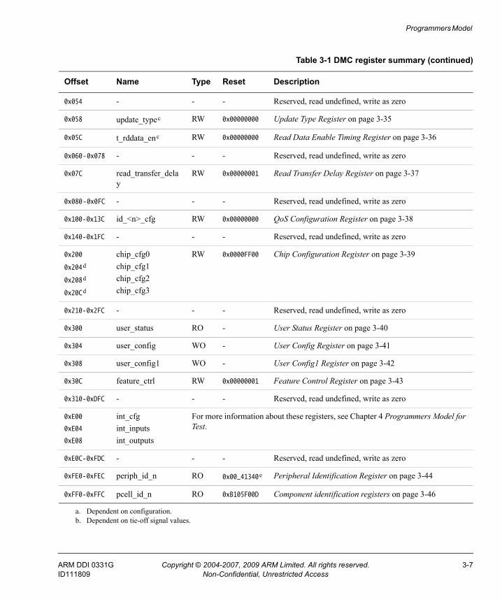
Programmers Model
0x054 - - - Reserved, read undefined, write as zero
0x058 update_typec RW 0x00000000 Update Type Register on page 3-35
0x05C t_rddata_enc RW 0x00000000 Read Data Enable Timing Register on page 3-36
0x060-0x078 - - - Reserved, read undefined, write as zero
0x07C read_transfer_delay
RW 0x00000001 Read Transfer Delay Register on page 3-37
0x080-0x0FC - - - Reserved, read undefined, write as zero
0x100-0x13C id_<n>_cfg RW 0x00000000 QoS Configuration Register on page 3-38
0x140-0x1FC - - - Reserved, read undefined, write as zero
0x200
0x204d
0x208d
0x20Cd
chip_cfg0chip_cfg1chip_cfg2chip_cfg3
RW 0x0000FF00 Chip Configuration Register on page 3-39
0x210-0x2FC - - - Reserved, read undefined, write as zero
0x300 user_status RO - User Status Register on page 3-40
0x304 user_config WO - User Config Register on page 3-41
0x308 user_config1 WO - User Config1 Register on page 3-42
0x30C feature_ctrl RW 0x00000001 Feature Control Register on page 3-43
0x310-0xDFC - - - Reserved, read undefined, write as zero
0xE00
0xE04
0xE08
int_cfgint_inputsint_outputs
For more information about these registers, see Chapter 4 Programmers Model for Test.
0xE0C-0xFDC - - - Reserved, read undefined, write as zero
0xFE0-0xFEC periph_id_n RO 0x00_41340e Peripheral Identification Register on page 3-44
0xFF0-0xFFC pcell_id_n RO 0xB105F00D Component identification registers on page 3-46
a. Dependent on configuration.b. Dependent on tie-off signal values.
Table 3-1 DMC register summary (continued)
Offset Name Type Reset Description
ARM DDI 0331G Copyright © 2004-2007, 2009 ARM Limited. All rights reserved. 3-7ID111809 Non-Confidential, Unrestricted Access
Programmers Model
c. This register is only present when the DMC is configured to implement a DDR PHY Interface (DFI), otherwise reads are undefined, write as zero.
d. The presence of this register depends on the number of chip selects that a configured controller supports. If a controller does not implement the register then reads are undefined, write as zero.
e. Dependent on the revision of the DMC, see Peripheral Identification Register 2 on page 3-46.
3-8 Copyright © 2004-2007, 2009 ARM Limited. All rights reserved. ARM DDI 0331GNon-Confidential, Unrestricted Access ID111809
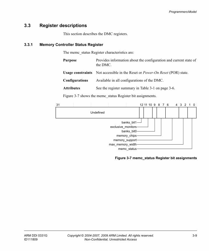
Programmers Model
3.3 Register descriptionsThis section describes the DMC registers.
3.3.1 Memory Controller Status Register
The memc_status Register characteristics are:
Purpose Provides information about the configuration and current state of the DMC.
Usage constraints Not accessible in the Reset or Power-On Reset (POR) state.
Configurations Available in all configurations of the DMC.
Attributes See the register summary in Table 3-1 on page 3-6.
Figure 3-7 shows the memc_status Register bit assignments.
Figure 3-7 memc_status Register bit assignments
memc_status
31 11 10 9 8 7 6 4 3 2 1 0
Undefined
exclusive_monitors
memory_chipsmemory_support
max_memory_width
12
banks_bit0
banks_bit1
ARM DDI 0331G Copyright © 2004-2007, 2009 ARM Limited. All rights reserved. 3-9ID111809 Non-Confidential, Unrestricted Access
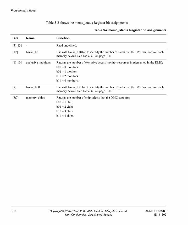
Programmers Model
Table 3-2 shows the memc_status Register bit assignments.
Table 3-2 memc_status Register bit assignments
Bits Name Function
[31:13] - Read undefined.
[12] banks_bit1 Use with banks_bit0 bit, to identify the number of banks that the DMC supports on each memory device. See Table 3-3 on page 3-11.
[11:10] exclusive_monitors Returns the number of exclusive access monitor resources implemented in the DMC:b00 = 0 monitorsb01 = 1 monitorb10 = 2 monitorsb11 = 4 monitors.
[9] banks_bit0 Use with banks_bit1 bit, to identify the number of banks that the DMC supports on each memory device. See Table 3-3 on page 3-11.
[8:7] memory_chips Returns the number of chip selects that the DMC supports:b00 = 1 chipb01 = 2 chipsb10 = 3 chipsb11 = 4 chips.
3-10 Copyright © 2004-2007, 2009 ARM Limited. All rights reserved. ARM DDI 0331GNon-Confidential, Unrestricted Access ID111809
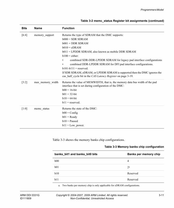
Programmers Model
Table 3-3 shows the memory banks chip configurations.
[6:4] memory_support Returns the type of SDRAM that the DMC supports:b000 = SDR SDRAMb001 = DDR SDRAMb010 = eDRAMb011 = LPDDR SDRAM, also known as mobile DDR SDRAMb100 = either:• combined SDR-DDR-LPDDR SDRAM for legacy pad interface configurations• combined DDR-LPDDR SDRAM for DFI pad interface configurations.b101-b111 = reserved.If SDR SDRAM, eDRAM, or LPDDR SDRAM is supported then the DMC ignores the cas_half_cycle bit in the CAS Latency Register on page 3-19.
[3:2] max_memory_width Returns the value of MEMWIDTH, that is, the memory data bus width of the pad interface that is set during configuration of the DMC:b00 = 16-bitb01 = 32-bitb10 = 64-bitb11 = reserved.
[1:0] memc_status Returns the state of the DMC:b00 = Configb01 = Readyb10 = Pausedb11 = Low_power.
Table 3-2 memc_status Register bit assignments (continued)
Bits Name Function
Table 3-3 Memory banks chip configuration
banks_bit1 and banks_bit0 bits Banks per memory chip
b00 4
b01 2a
a. Two banks per memory chip is only applicable for eDRAM configurations.
b10 Reserved
b11 Reserved
ARM DDI 0331G Copyright © 2004-2007, 2009 ARM Limited. All rights reserved. 3-11ID111809 Non-Confidential, Unrestricted Access
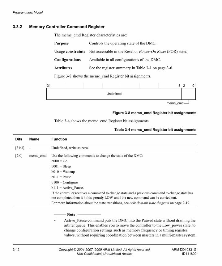
Programmers Model
3.3.2 Memory Controller Command Register
The memc_cmd Register characteristics are:
Purpose Controls the operating state of the DMC.
Usage constraints Not accessible in the Reset or Power-On Reset (POR) state.
Configurations Available in all configurations of the DMC.
Attributes See the register summary in Table 3-1 on page 3-6.
Figure 3-8 shows the memc_cmd Register bit assignments.
Figure 3-8 memc_cmd Register bit assignments
Table 3-4 shows the memc_cmd Register bit assignments.
Note • Active_Pause command puts the DMC into the Paused state without draining the
arbiter queue. This enables you to move the controller to the Low_power state, to change configuration settings such as memory frequency or timing register values, without requiring coordination between masters in a multi-master system.
31 2 0
Undefined
memc_cmd
3
Table 3-4 memc_cmd Register bit assignments
Bits Name Function
[31:3] - Undefined, write as zero.
[2:0] memc_cmd Use the following commands to change the state of the DMC:b000 = Gob001 = Sleepb010 = Wakeupb011 = Pauseb100 = Configureb111 = Active_Pause.If the controller receives a command to change state and a previous command to change state has not completed then it holds pready LOW until the new command can be carried out.For more information about the state transitions, see aclk domain state diagram on page 2-19.
3-12 Copyright © 2004-2007, 2009 ARM Limited. All rights reserved. ARM DDI 0331GNon-Confidential, Unrestricted Access ID111809
Programmers Model
• If you use the Active_Pause command to put the DMC in the Low_power state then you must not remove power from the DMC because this results in data loss and violation of the AXI protocol.
• The DMC does not issue refreshes when in the Config state. Therefore, ARM recommends that you make register updates with the controller in Low_power state because this ensures that the memory is put into self-refresh mode, rather than the Config state when the memory contains valid data.
3.3.3 Direct Command Register
The direct_cmd Register characteristics are:
Purpose Initializes and updates the external memory devices by sending the following commands:• NOP
• PRECHARGEALL
• AUTO REFRESH
• MODEREG
• DPD.
Usage constraints Only accessible in Config state.
Configurations Available in all configurations of the DMC.
Attributes See the register summary in Table 3-1 on page 3-6.
The direct_cmd Register therefore enables any initialization sequence that an external memory device might require. The only timing information associated with the direct_cmd Register are the command delays that are programmed in the timing registers. Figure 3-2 on page 3-3 shows the timing registers. Therefore, if an initialization sequence requires additional delays between commands, they must be timed by the master driving the initialization sequence.
Figure 3-9 on page 3-14 shows the direct_cmd Register bit assignments.
ARM DDI 0331G Copyright © 2004-2007, 2009 ARM Limited. All rights reserved. 3-13ID111809 Non-Confidential, Unrestricted Access
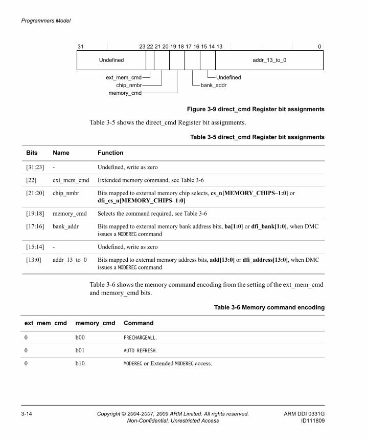
Programmers Model
Figure 3-9 direct_cmd Register bit assignments
Table 3-5 shows the direct_cmd Register bit assignments.
Table 3-6 shows the memory command encoding from the setting of the ext_mem_cmd and memory_cmd bits.
31 23 22 21 20 19 18 17 15 14 13 0
Undefined
ext_mem_cmd
memory_cmdchip_nmbr
addr_13_to_0
Undefinedbank_addr
16
Table 3-5 direct_cmd Register bit assignments
Bits Name Function
[31:23] - Undefined, write as zero
[22] ext_mem_cmd Extended memory command, see Table 3-6
[21:20] chip_nmbr Bits mapped to external memory chip selects, cs_n[MEMORY_CHIPS–1:0] or dfi_cs_n[MEMORY_CHIPS–1:0]
[19:18] memory_cmd Selects the command required, see Table 3-6
[17:16] bank_addr Bits mapped to external memory bank address bits, ba[1:0] or dfi_bank[1:0], when DMC issues a MODEREG command
[15:14] - Undefined, write as zero
[13:0] addr_13_to_0 Bits mapped to external memory address bits, add[13:0] or dfi_address[13:0], when DMC issues a MODEREG command
Table 3-6 Memory command encoding
ext_mem_cmd memory_cmd Command
0 b00 PRECHARGEALL.
0 b01 AUTO REFRESH.
0 b10 MODEREG or Extended MODEREG access.
3-14 Copyright © 2004-2007, 2009 ARM Limited. All rights reserved. ARM DDI 0331GNon-Confidential, Unrestricted Access ID111809
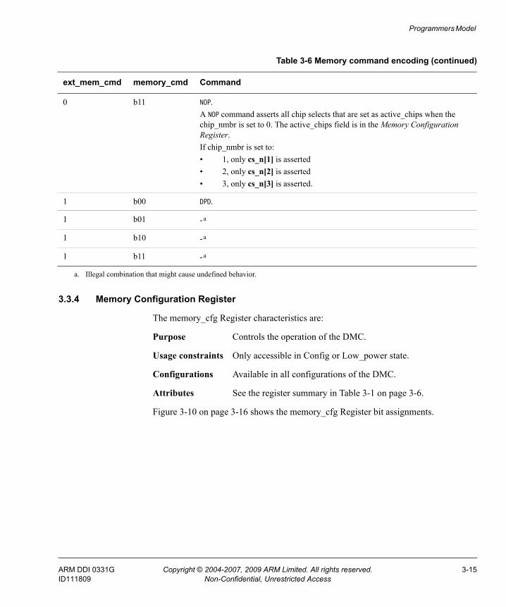
Programmers Model
3.3.4 Memory Configuration Register
The memory_cfg Register characteristics are:
Purpose Controls the operation of the DMC.
Usage constraints Only accessible in Config or Low_power state.
Configurations Available in all configurations of the DMC.
Attributes See the register summary in Table 3-1 on page 3-6.
Figure 3-10 on page 3-16 shows the memory_cfg Register bit assignments.
0 b11 NOP.A NOP command asserts all chip selects that are set as active_chips when the chip_nmbr is set to 0. The active_chips field is in the Memory Configuration Register.If chip_nmbr is set to:• 1, only cs_n[1] is asserted• 2, only cs_n[2] is asserted• 3, only cs_n[3] is asserted.
1 b00 DPD.
1 b01 -a
1 b10 -a
1 b11 -a
a. Illegal combination that might cause undefined behavior.
Table 3-6 Memory command encoding (continued)
ext_mem_cmd memory_cmd Command
ARM DDI 0331G Copyright © 2004-2007, 2009 ARM Limited. All rights reserved. 3-15ID111809 Non-Confidential, Unrestricted Access
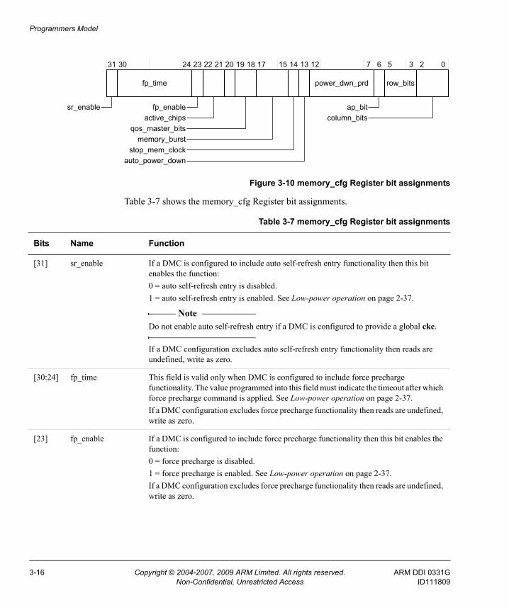
Programmers Model
Figure 3-10 memory_cfg Register bit assignments
Table 3-7 shows the memory_cfg Register bit assignments.
31 23 22 21 20 19 18 17 15 14 13 12 7 6 5 3 2 0
fp_time
memory_burstqos_master_bits
active_chips
stop_mem_clockauto_power_down
power_dwn_prd
ap_bit
row_bits
column_bitssr_enable fp_enable
30 24
Table 3-7 memory_cfg Register bit assignments
Bits Name Function
[31] sr_enable If a DMC is configured to include auto self-refresh entry functionality then this bit enables the function:0 = auto self-refresh entry is disabled.1 = auto self-refresh entry is enabled. See Low-power operation on page 2-37.
Note Do not enable auto self-refresh entry if a DMC is configured to provide a global cke.
If a DMC configuration excludes auto self-refresh entry functionality then reads are undefined, write as zero.
[30:24] fp_time This field is valid only when DMC is configured to include force precharge functionality. The value programmed into this field must indicate the timeout after which force precharge command is applied. See Low-power operation on page 2-37.If a DMC configuration excludes force precharge functionality then reads are undefined, write as zero.
[23] fp_enable If a DMC is configured to include force precharge functionality then this bit enables the function:0 = force precharge is disabled.1 = force precharge is enabled. See Low-power operation on page 2-37.If a DMC configuration excludes force precharge functionality then reads are undefined, write as zero.
3-16 Copyright © 2004-2007, 2009 ARM Limited. All rights reserved. ARM DDI 0331GNon-Confidential, Unrestricted Access ID111809
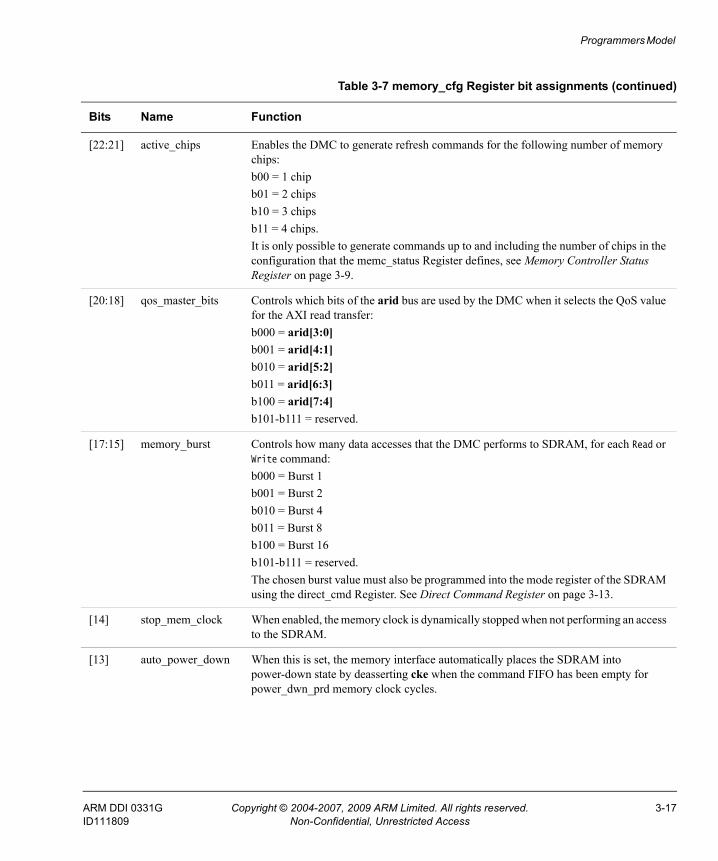
Programmers Model
[22:21] active_chips Enables the DMC to generate refresh commands for the following number of memory chips:b00 = 1 chipb01 = 2 chipsb10 = 3 chipsb11 = 4 chips.It is only possible to generate commands up to and including the number of chips in the configuration that the memc_status Register defines, see Memory Controller Status Register on page 3-9.
[20:18] qos_master_bits Controls which bits of the arid bus are used by the DMC when it selects the QoS value for the AXI read transfer:b000 = arid[3:0]b001 = arid[4:1]b010 = arid[5:2]b011 = arid[6:3]b100 = arid[7:4]b101-b111 = reserved.
[17:15] memory_burst Controls how many data accesses that the DMC performs to SDRAM, for each Read or Write command:b000 = Burst 1b001 = Burst 2b010 = Burst 4b011 = Burst 8b100 = Burst 16b101-b111 = reserved.The chosen burst value must also be programmed into the mode register of the SDRAM using the direct_cmd Register. See Direct Command Register on page 3-13.
[14] stop_mem_clock When enabled, the memory clock is dynamically stopped when not performing an access to the SDRAM.
[13] auto_power_down When this is set, the memory interface automatically places the SDRAM into power-down state by deasserting cke when the command FIFO has been empty for power_dwn_prd memory clock cycles.
Table 3-7 memory_cfg Register bit assignments (continued)
Bits Name Function
ARM DDI 0331G Copyright © 2004-2007, 2009 ARM Limited. All rights reserved. 3-17ID111809 Non-Confidential, Unrestricted Access
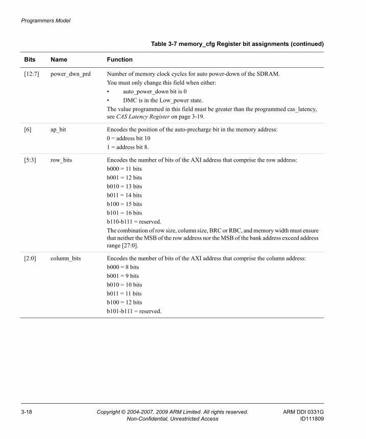
Programmers Model
[12:7] power_dwn_prd Number of memory clock cycles for auto power-down of the SDRAM.You must only change this field when either:• auto_power_down bit is 0• DMC is in the Low_power state.The value programmed in this field must be greater than the programmed cas_latency, see CAS Latency Register on page 3-19.
[6] ap_bit Encodes the position of the auto-precharge bit in the memory address:0 = address bit 101 = address bit 8.
[5:3] row_bits Encodes the number of bits of the AXI address that comprise the row address:b000 = 11 bitsb001 = 12 bitsb010 = 13 bitsb011 = 14 bitsb100 = 15 bitsb101 = 16 bitsb110-b111 = reserved.The combination of row size, column size, BRC or RBC, and memory width must ensure that neither the MSB of the row address nor the MSB of the bank address exceed address range [27:0].
[2:0] column_bits Encodes the number of bits of the AXI address that comprise the column address:b000 = 8 bitsb001 = 9 bitsb010 = 10 bitsb011 = 11 bitsb100 = 12 bitsb101-b111 = reserved.
Table 3-7 memory_cfg Register bit assignments (continued)
Bits Name Function
3-18 Copyright © 2004-2007, 2009 ARM Limited. All rights reserved. ARM DDI 0331GNon-Confidential, Unrestricted Access ID111809
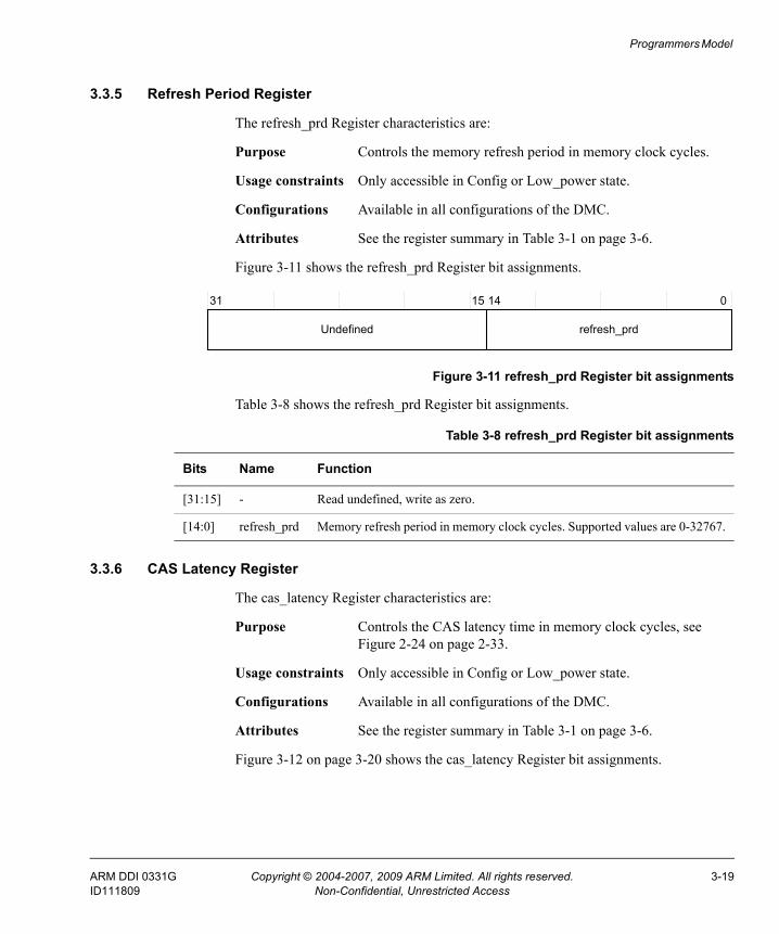
Programmers Model
3.3.5 Refresh Period Register
The refresh_prd Register characteristics are:
Purpose Controls the memory refresh period in memory clock cycles.
Usage constraints Only accessible in Config or Low_power state.
Configurations Available in all configurations of the DMC.
Attributes See the register summary in Table 3-1 on page 3-6.
Figure 3-11 shows the refresh_prd Register bit assignments.
Figure 3-11 refresh_prd Register bit assignments
Table 3-8 shows the refresh_prd Register bit assignments.
3.3.6 CAS Latency Register
The cas_latency Register characteristics are:
Purpose Controls the CAS latency time in memory clock cycles, see Figure 2-24 on page 2-33.
Usage constraints Only accessible in Config or Low_power state.
Configurations Available in all configurations of the DMC.
Attributes See the register summary in Table 3-1 on page 3-6.
Figure 3-12 on page 3-20 shows the cas_latency Register bit assignments.
refresh_prd
31 15 14 0
Undefined
Table 3-8 refresh_prd Register bit assignments
Bits Name Function
[31:15] - Read undefined, write as zero.
[14:0] refresh_prd Memory refresh period in memory clock cycles. Supported values are 0-32767.
ARM DDI 0331G Copyright © 2004-2007, 2009 ARM Limited. All rights reserved. 3-19ID111809 Non-Confidential, Unrestricted Access
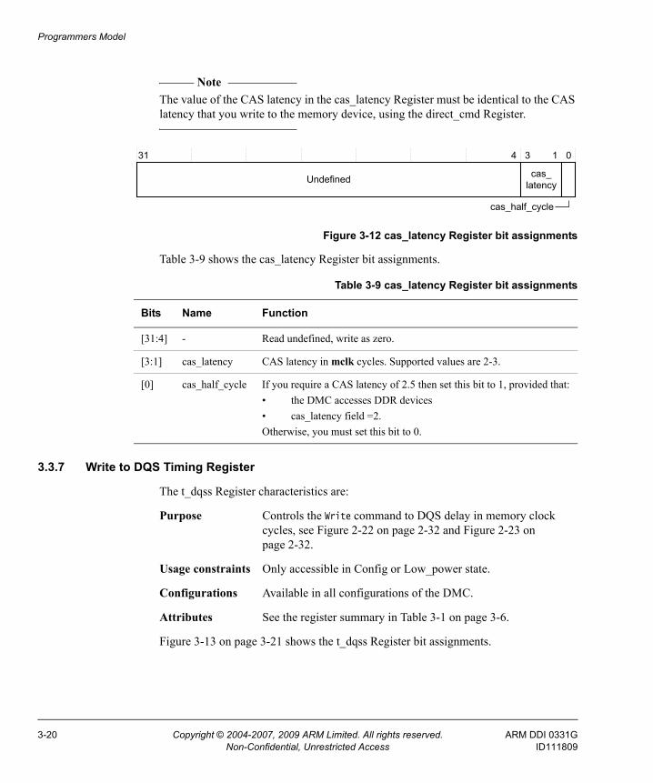
Programmers Model
Note The value of the CAS latency in the cas_latency Register must be identical to the CAS latency that you write to the memory device, using the direct_cmd Register.
Figure 3-12 cas_latency Register bit assignments
Table 3-9 shows the cas_latency Register bit assignments.
3.3.7 Write to DQS Timing Register
The t_dqss Register characteristics are:
Purpose Controls the Write command to DQS delay in memory clock cycles, see Figure 2-22 on page 2-32 and Figure 2-23 on page 2-32.
Usage constraints Only accessible in Config or Low_power state.
Configurations Available in all configurations of the DMC.
Attributes See the register summary in Table 3-1 on page 3-6.
Figure 3-13 on page 3-21 shows the t_dqss Register bit assignments.
Undefined
31 4 3 1 0
cas_half_cycle
cas_latency
Table 3-9 cas_latency Register bit assignments
Bits Name Function
[31:4] - Read undefined, write as zero.
[3:1] cas_latency CAS latency in mclk cycles. Supported values are 2-3.
[0] cas_half_cycle If you require a CAS latency of 2.5 then set this bit to 1, provided that:• the DMC accesses DDR devices• cas_latency field =2.Otherwise, you must set this bit to 0.
3-20 Copyright © 2004-2007, 2009 ARM Limited. All rights reserved. ARM DDI 0331GNon-Confidential, Unrestricted Access ID111809
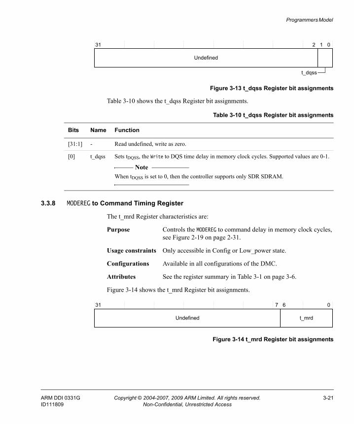
Programmers Model
Figure 3-13 t_dqss Register bit assignments
Table 3-10 shows the t_dqss Register bit assignments.
3.3.8 MODEREG to Command Timing Register
The t_mrd Register characteristics are:
Purpose Controls the MODEREG to command delay in memory clock cycles, see Figure 2-19 on page 2-31.
Usage constraints Only accessible in Config or Low_power state.
Configurations Available in all configurations of the DMC.
Attributes See the register summary in Table 3-1 on page 3-6.
Figure 3-14 shows the t_mrd Register bit assignments.
Figure 3-14 t_mrd Register bit assignments
Undefined
31 2 1 0
t_dqss
Table 3-10 t_dqss Register bit assignments
Bits Name Function
[31:1] - Read undefined, write as zero.
[0] t_dqss Sets tDQSS, the Write to DQS time delay in memory clock cycles. Supported values are 0-1.
Note When tDQSS is set to 0, then the controller supports only SDR SDRAM.
t_mrd
31 7 0
Undefined
6
ARM DDI 0331G Copyright © 2004-2007, 2009 ARM Limited. All rights reserved. 3-21ID111809 Non-Confidential, Unrestricted Access
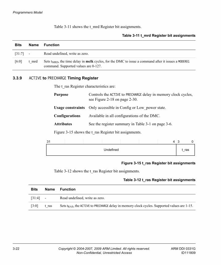
Programmers Model
Table 3-11 shows the t_mrd Register bit assignments.
3.3.9 ACTIVE to PRECHARGE Timing Register
The t_ras Register characteristics are:
Purpose Controls the ACTIVE to PRECHARGE delay in memory clock cycles, see Figure 2-18 on page 2-30.
Usage constraints Only accessible in Config or Low_power state.
Configurations Available in all configurations of the DMC.
Attributes See the register summary in Table 3-1 on page 3-6.
Figure 3-15 shows the t_ras Register bit assignments.
Figure 3-15 t_ras Register bit assignments
Table 3-12 shows the t_ras Register bit assignments.
Table 3-11 t_mrd Register bit assignments
Bits Name Function
[31:7] - Read undefined, write as zero.
[6:0] t_mrd Sets tMRD, the time delay in mclk cycles, for the DMC to issue a command after it issues a MODEREG command. Supported values are 0-127.
t_ras
31 4 0
Undefined
3
Table 3-12 t_ras Register bit assignments
Bits Name Function
[31:4] - Read undefined, write as zero.
[3:0] t_ras Sets tRAS, the ACTIVE to PRECHARGE delay in memory clock cycles. Supported values are 1-15.
3-22 Copyright © 2004-2007, 2009 ARM Limited. All rights reserved. ARM DDI 0331GNon-Confidential, Unrestricted Access ID111809
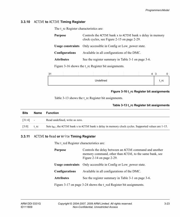
Programmers Model
3.3.10 ACTIVE to ACTIVE Timing Register
The t_rc Register characteristics are:
Purpose Controls the ACTIVE bank x to ACTIVE bank x delay in memory clock cycles, see Figure 2-15 on page 2-29.
Usage constraints Only accessible in Config or Low_power state.
Configurations Available in all configurations of the DMC.
Attributes See the register summary in Table 3-1 on page 3-6.
Figure 3-16 shows the t_rc Register bit assignments.
Figure 3-16 t_rc Register bit assignments
Table 3-13 shows the t_rc Register bit assignments.
3.3.11 ACTIVE to Read or Write Timing Register
The t_rcd Register characteristics are:
Purpose Controls the delay between an ACTIVE command and another memory command, other than ACTIVE, to the same bank, see Figure 2-14 on page 2-29.
Usage constraints Only accessible in Config or Low_power state.
Configurations Available in all configurations of the DMC.
Attributes See the register summary in Table 3-1 on page 3-6.
Figure 3-17 on page 3-24 shows the t_rcd Register bit assignments.
t_rc
31 4 0
Undefined
3
Table 3-13 t_rc Register bit assignments
Bits Name Function
[31:4] - Read undefined, write as zero.
[3:0] t_rc Sets tRC, the ACTIVE bank x to ACTIVE bank x delay in memory clock cycles. Supported values are 1-15.
ARM DDI 0331G Copyright © 2004-2007, 2009 ARM Limited. All rights reserved. 3-23ID111809 Non-Confidential, Unrestricted Access
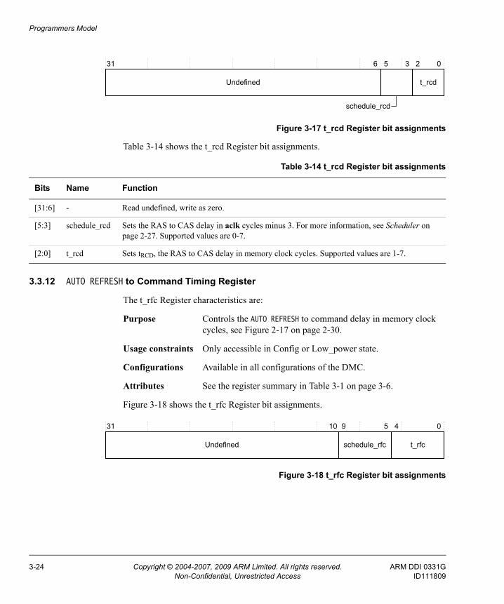
Programmers Model
Figure 3-17 t_rcd Register bit assignments
Table 3-14 shows the t_rcd Register bit assignments.
3.3.12 AUTO REFRESH to Command Timing Register
The t_rfc Register characteristics are:
Purpose Controls the AUTO REFRESH to command delay in memory clock cycles, see Figure 2-17 on page 2-30.
Usage constraints Only accessible in Config or Low_power state.
Configurations Available in all configurations of the DMC.
Attributes See the register summary in Table 3-1 on page 3-6.
Figure 3-18 shows the t_rfc Register bit assignments.
Figure 3-18 t_rfc Register bit assignments
t_rcd
31 3 0
Undefined
256
schedule_rcd
Table 3-14 t_rcd Register bit assignments
Bits Name Function
[31:6] - Read undefined, write as zero.
[5:3] schedule_rcd Sets the RAS to CAS delay in aclk cycles minus 3. For more information, see Scheduler on page 2-27. Supported values are 0-7.
[2:0] t_rcd Sets tRCD, the RAS to CAS delay in memory clock cycles. Supported values are 1-7.
31 9 0410 5
t_rfcschedule_rfcUndefined
3-24 Copyright © 2004-2007, 2009 ARM Limited. All rights reserved. ARM DDI 0331GNon-Confidential, Unrestricted Access ID111809
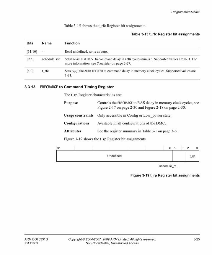
Programmers Model
Table 3-15 shows the t_rfc Register bit assignments.
3.3.13 PRECHARGE to Command Timing Register
The t_rp Register characteristics are:
Purpose Controls the PRECHARGE to RAS delay in memory clock cycles, see Figure 2-17 on page 2-30 and Figure 2-18 on page 2-30.
Usage constraints Only accessible in Config or Low_power state.
Configurations Available in all configurations of the DMC.
Attributes See the register summary in Table 3-1 on page 3-6.
Figure 3-19 shows the t_rp Register bit assignments.
Figure 3-19 t_rp Register bit assignments
Table 3-15 t_rfc Register bit assignments
Bits Name Function
[31:10] - Read undefined, write as zero.
[9:5] schedule_rfc Sets the AUTO REFRESH to command delay in aclk cycles minus 3. Supported values are 0-31. For more information, see Scheduler on page 2-27.
[4:0] t_rfc Sets tRFC, the AUTO REFRESH to command delay in memory clock cycles. Supported values are 1-31.
Undefined t_rp
31 3 0256
schedule_rp
ARM DDI 0331G Copyright © 2004-2007, 2009 ARM Limited. All rights reserved. 3-25ID111809 Non-Confidential, Unrestricted Access
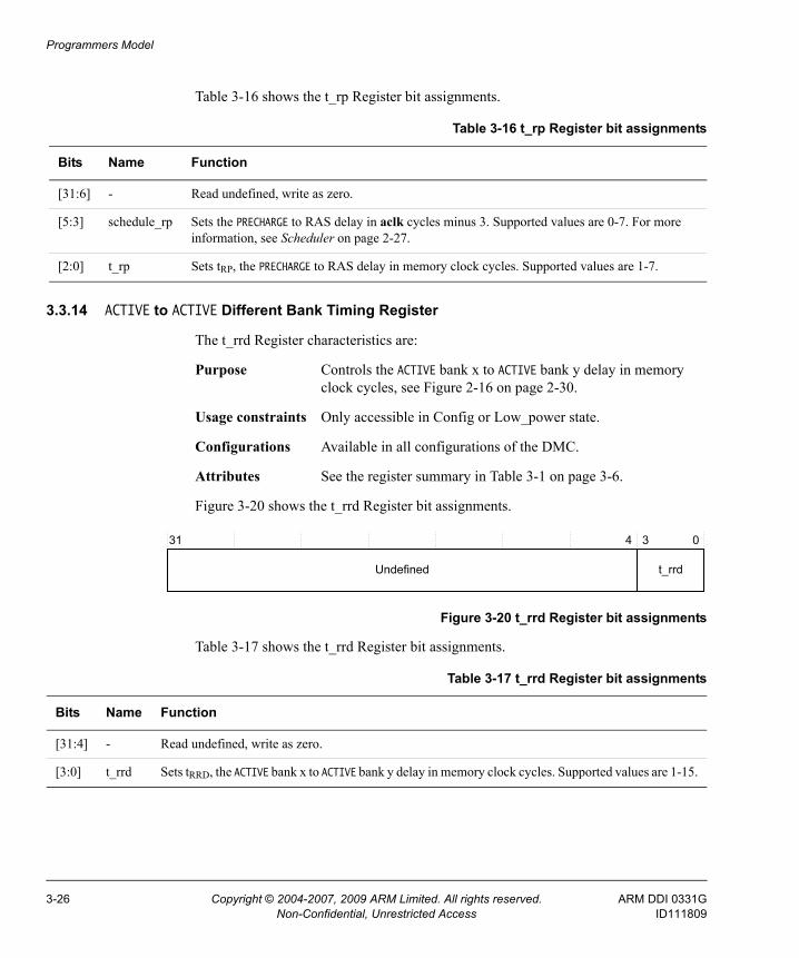
Programmers Model
Table 3-16 shows the t_rp Register bit assignments.
3.3.14 ACTIVE to ACTIVE Different Bank Timing Register
The t_rrd Register characteristics are:
Purpose Controls the ACTIVE bank x to ACTIVE bank y delay in memory clock cycles, see Figure 2-16 on page 2-30.
Usage constraints Only accessible in Config or Low_power state.
Configurations Available in all configurations of the DMC.
Attributes See the register summary in Table 3-1 on page 3-6.
Figure 3-20 shows the t_rrd Register bit assignments.
Figure 3-20 t_rrd Register bit assignments
Table 3-17 shows the t_rrd Register bit assignments.
Table 3-16 t_rp Register bit assignments
Bits Name Function
[31:6] - Read undefined, write as zero.
[5:3] schedule_rp Sets the PRECHARGE to RAS delay in aclk cycles minus 3. Supported values are 0-7. For more information, see Scheduler on page 2-27.
[2:0] t_rp Sets tRP, the PRECHARGE to RAS delay in memory clock cycles. Supported values are 1-7.
Undefined t_rrd
31 4 03
Table 3-17 t_rrd Register bit assignments
Bits Name Function
[31:4] - Read undefined, write as zero.
[3:0] t_rrd Sets tRRD, the ACTIVE bank x to ACTIVE bank y delay in memory clock cycles. Supported values are 1-15.
3-26 Copyright © 2004-2007, 2009 ARM Limited. All rights reserved. ARM DDI 0331GNon-Confidential, Unrestricted Access ID111809
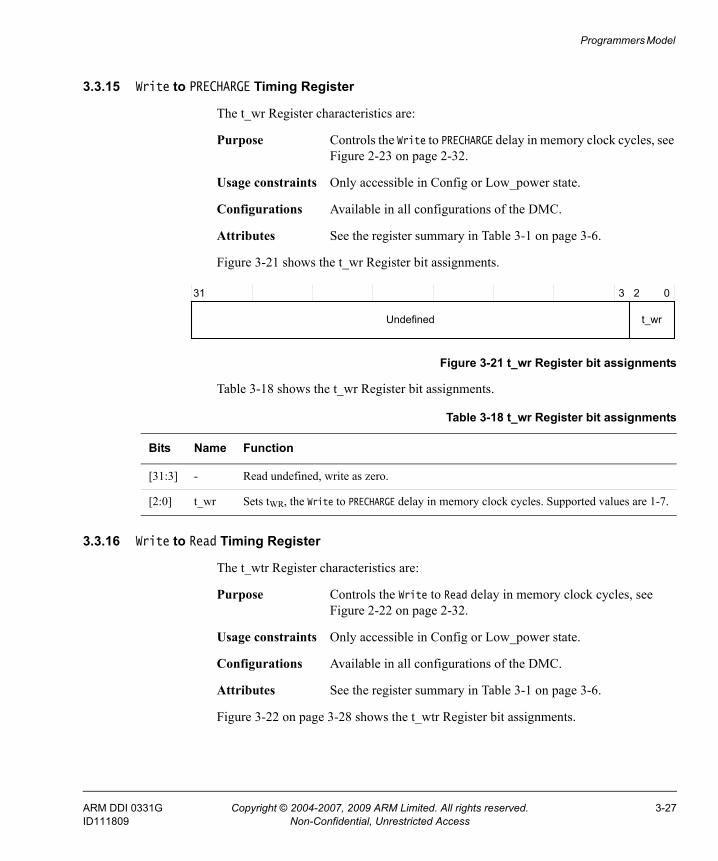
Programmers Model
3.3.15 Write to PRECHARGE Timing Register
The t_wr Register characteristics are:
Purpose Controls the Write to PRECHARGE delay in memory clock cycles, see Figure 2-23 on page 2-32.
Usage constraints Only accessible in Config or Low_power state.
Configurations Available in all configurations of the DMC.
Attributes See the register summary in Table 3-1 on page 3-6.
Figure 3-21 shows the t_wr Register bit assignments.
Figure 3-21 t_wr Register bit assignments
Table 3-18 shows the t_wr Register bit assignments.
3.3.16 Write to Read Timing Register
The t_wtr Register characteristics are:
Purpose Controls the Write to Read delay in memory clock cycles, see Figure 2-22 on page 2-32.
Usage constraints Only accessible in Config or Low_power state.
Configurations Available in all configurations of the DMC.
Attributes See the register summary in Table 3-1 on page 3-6.
Figure 3-22 on page 3-28 shows the t_wtr Register bit assignments.
t_wr
31 3 02
Undefined
Table 3-18 t_wr Register bit assignments
Bits Name Function
[31:3] - Read undefined, write as zero.
[2:0] t_wr Sets tWR, the Write to PRECHARGE delay in memory clock cycles. Supported values are 1-7.
ARM DDI 0331G Copyright © 2004-2007, 2009 ARM Limited. All rights reserved. 3-27ID111809 Non-Confidential, Unrestricted Access
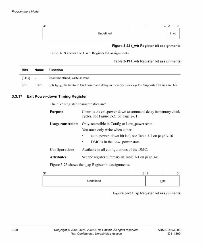
Programmers Model
Figure 3-22 t_wtr Register bit assignments
Table 3-19 shows the t_wtr Register bit assignments.
3.3.17 Exit Power-down Timing Register
The t_xp Register characteristics are:
Purpose Controls the exit power-down to command delay in memory clock cycles, see Figure 2-21 on page 2-31.
Usage constraints Only accessible in Config or Low_power state.You must only write when either:• auto_power_down bit is 0, see Table 3-7 on page 3-16• DMC is in the Low_power state.
Configurations Available in all configurations of the DMC.
Attributes See the register summary in Table 3-1 on page 3-6.
Figure 3-23 shows the t_xp Register bit assignments.
Figure 3-23 t_xp Register bit assignments
t_wtr
31 3 02
Undefined
Table 3-19 t_wtr Register bit assignments
Bits Name Function
[31:3] - Read undefined, write as zero.
[2:0] t_wtr Sets tWTR, the Write to Read command delay in memory clock cycles. Supported values are 1-7.
t_xp
31 8 07
Undefined
3-28 Copyright © 2004-2007, 2009 ARM Limited. All rights reserved. ARM DDI 0331GNon-Confidential, Unrestricted Access ID111809
Programmers Model
Table 3-20 shows the t_xp Register bit assignments.
3.3.18 Exit Self-refresh Timing Register
The t_xsr Register characteristics are:
Purpose Controls the exit self-refresh to command delay in memory clock cycles, see Figure 2-20 on page 2-31.
Usage constraints Only accessible in Config or Low_power state.
Configurations Available in all configurations of the DMC.
Attributes See the register summary in Table 3-1 on page 3-6.
Figure 3-24 shows the t_xsr Register bit assignments.
Figure 3-24 t_xsr Register bit assignments
Table 3-21 shows the t_xsr Register bit assignments.
Table 3-20 t_xp Register bit assignments
Bits Name Function
[31:8] - Read undefined, write as zero.
[7:0] t_xp Sets tXP, the exit power-down to command delay in memory clock cycles. Supported values are 1-255.
t_xsr
31 8 07
Undefined
Table 3-21 t_xsr Register bit assignments
Bits Name Function
[31:8] - Read undefined, write as zero.
[7:0] t_xsr Sets tXSR, the exit self-refresh to command delay in memory clock cycles. Supported values are 1-255.
ARM DDI 0331G Copyright © 2004-2007, 2009 ARM Limited. All rights reserved. 3-29ID111809 Non-Confidential, Unrestricted Access
Programmers Model
3.3.19 Self-refresh to Command Timing Register
The t_esr Register characteristics are:
Purpose Controls the self-refresh to command delay in memory clock cycles, see Figure 2-20 on page 2-31.
Usage constraints Only accessible in Config or Low_power state.
Configurations Available in all configurations of the DMC.
Attributes See the register summary in Table 3-1 on page 3-6.
Figure 3-25 shows the t_esr Register bit assignments.
Figure 3-25 t_esr Register bit assignments
Table 3-22 shows the t_esr Register bit assignments.
3.3.20 Memory Configuration 2 Register
The memory_cfg2 Register characteristics are:
Purpose Controls the operation of the DMC. Enables you to override the configuration set by the tie-off signals, see Tie-offs on page A-3.
Usage constraints • Only accessible in Config or Low_power state.• Some bits are only available when a DMC is configured to
provide a legacy pad interface.
Configurations Available in all configurations of the DMC.
Attributes See the register summary in Table 3-1 on page 3-6.
Figure 3-26 on page 3-31 shows the memory_cfg2 Register bit assignments.
31 8 07
Undefined t_esr
Table 3-22 t_esr Register bit assignments
Bits Name Function
[31:8] - Read undefined, write as zero.
[7:0] t_esr Sets the self-refresh to command delay in memory clock cycles. Supported values are 1-255.
3-30 Copyright © 2004-2007, 2009 ARM Limited. All rights reserved. ARM DDI 0331GNon-Confidential, Unrestricted Access ID111809
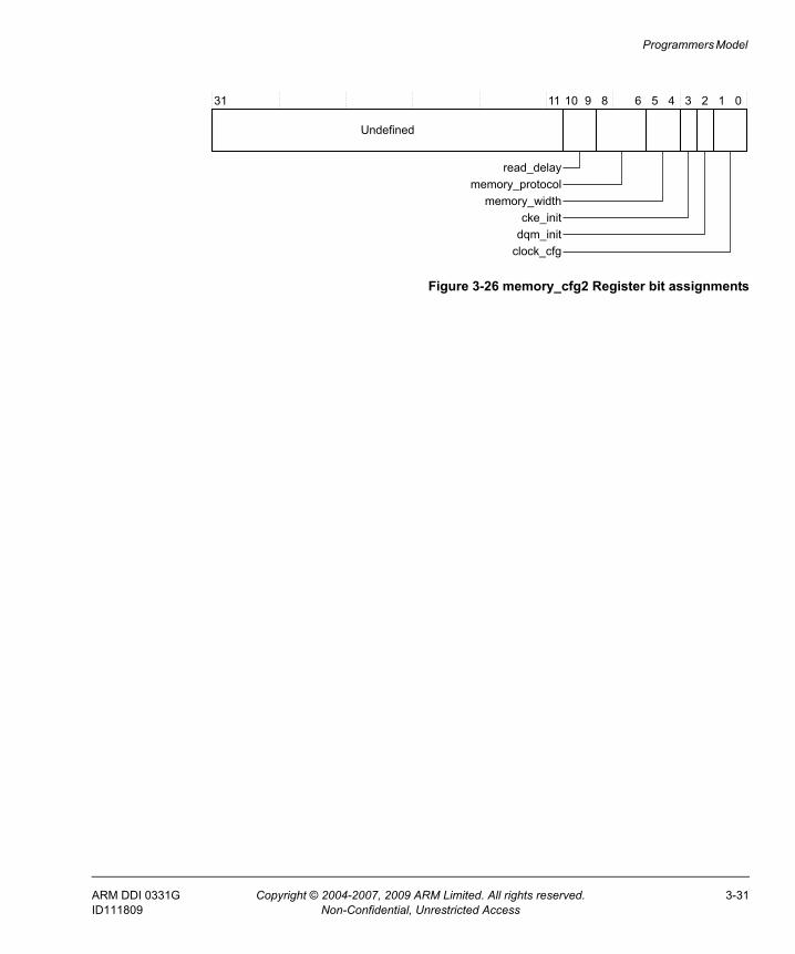
Programmers Model
Figure 3-26 memory_cfg2 Register bit assignments
31 11 10 8 6 5 4 3 2 1 0
Undefined
memory_protocolmemory_width
cke_initdqm_init
clock_cfg
read_delay
9
ARM DDI 0331G Copyright © 2004-2007, 2009 ARM Limited. All rights reserved. 3-31ID111809 Non-Confidential, Unrestricted Access
Programmers Model
Table 3-23 shows the memory_cfg2 Register bit assignments.
Table 3-23 memory_cfg2 Register bit assignments
Bits Name Function
[31:11] - Read undefined, write as zero.
[10:9] read_delay This field varies the number of mclk cycles before the controller captures the read data, from the memory device, into the memory clock domain. Supported values are 0-2.The default value is set by the state of read_delay[1:0], when aresetn goes HIGH.
[8:6] memory_protocol If a configured DMC supports combined SDR-DDR-LPDDR SDRAM or combined DDR-LPDDR SDRAM then you can use this field to modify the memory protocol that it supports.The memory protocol encodings are:• b000 = SDR• b001 = DDR• b010 = eDRAM• b011 = LPDDR, also known as mobile DDR• b100 = either:
— combined SDR-DDR-LPDDR SDRAM for legacy pad interface configurations
— combined DDR-LPDDR SDRAM for DFI pad interface configurations.• b101-b111 = reserved.The default value is set by the state of memory_type[2:0], when aresetn goes HIGH.
Note • You can use the memory_support field to determine what memory protocols a
configured controller supports, see Memory Controller Status Register on page 3-9.• Selecting a memory protocol that the configured DMC does not support can result
in Unpredictable behavior.
3-32 Copyright © 2004-2007, 2009 ARM Limited. All rights reserved. ARM DDI 0331GNon-Confidential, Unrestricted Access ID111809
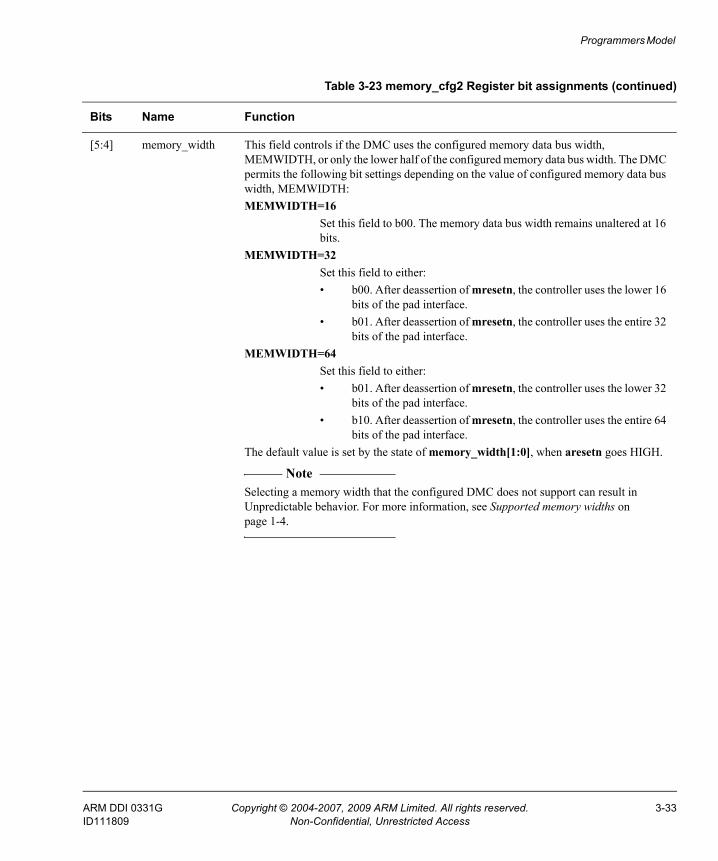
Programmers Model
[5:4] memory_width This field controls if the DMC uses the configured memory data bus width, MEMWIDTH, or only the lower half of the configured memory data bus width. The DMC permits the following bit settings depending on the value of configured memory data bus width, MEMWIDTH:MEMWIDTH=16
Set this field to b00. The memory data bus width remains unaltered at 16 bits.
MEMWIDTH=32 Set this field to either:• b00. After deassertion of mresetn, the controller uses the lower 16
bits of the pad interface.• b01. After deassertion of mresetn, the controller uses the entire 32
bits of the pad interface.MEMWIDTH=64
Set this field to either:• b01. After deassertion of mresetn, the controller uses the lower 32
bits of the pad interface.• b10. After deassertion of mresetn, the controller uses the entire 64
bits of the pad interface.The default value is set by the state of memory_width[1:0], when aresetn goes HIGH.
Note Selecting a memory width that the configured DMC does not support can result in Unpredictable behavior. For more information, see Supported memory widths on page 1-4.
Table 3-23 memory_cfg2 Register bit assignments (continued)
Bits Name Function
ARM DDI 0331G Copyright © 2004-2007, 2009 ARM Limited. All rights reserved. 3-33ID111809 Non-Confidential, Unrestricted Access
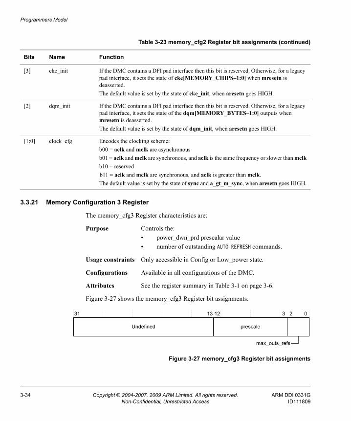
Programmers Model
3.3.21 Memory Configuration 3 Register
The memory_cfg3 Register characteristics are:
Purpose Controls the:• power_dwn_prd prescalar value• number of outstanding AUTO REFRESH commands.
Usage constraints Only accessible in Config or Low_power state.
Configurations Available in all configurations of the DMC.
Attributes See the register summary in Table 3-1 on page 3-6.
Figure 3-27 shows the memory_cfg3 Register bit assignments.
Figure 3-27 memory_cfg3 Register bit assignments
[3] cke_init If the DMC contains a DFI pad interface then this bit is reserved. Otherwise, for a legacy pad interface, it sets the state of cke[MEMORY_CHIPS–1:0] when mresetn is deasserted.The default value is set by the state of cke_init, when aresetn goes HIGH.
[2] dqm_init If the DMC contains a DFI pad interface then this bit is reserved. Otherwise, for a legacy pad interface, it sets the state of the dqm[MEMORY_BYTES–1:0] outputs when mresetn is deasserted.The default value is set by the state of dqm_init, when aresetn goes HIGH.
[1:0] clock_cfg Encodes the clocking scheme:b00 = aclk and mclk are asynchronousb01 = aclk and mclk are synchronous, and aclk is the same frequency or slower than mclkb10 = reservedb11 = aclk and mclk are synchronous, and aclk is greater than mclk.The default value is set by the state of sync and a_gt_m_sync, when aresetn goes HIGH.
Table 3-23 memory_cfg2 Register bit assignments (continued)
Bits Name Function
31 3 2 0
Undefined prescale
max_outs_refs
13 12
3-34 Copyright © 2004-2007, 2009 ARM Limited. All rights reserved. ARM DDI 0331GNon-Confidential, Unrestricted Access ID111809
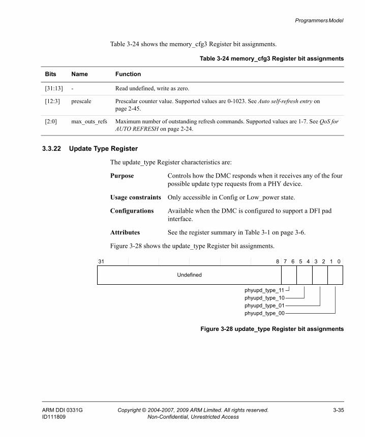
Programmers Model
Table 3-24 shows the memory_cfg3 Register bit assignments.
3.3.22 Update Type Register
The update_type Register characteristics are:
Purpose Controls how the DMC responds when it receives any of the four possible update type requests from a PHY device.
Usage constraints Only accessible in Config or Low_power state.
Configurations Available when the DMC is configured to support a DFI pad interface.
Attributes See the register summary in Table 3-1 on page 3-6.
Figure 3-28 shows the update_type Register bit assignments.
Figure 3-28 update_type Register bit assignments
Table 3-24 memory_cfg3 Register bit assignments
Bits Name Function
[31:13] - Read undefined, write as zero.
[12:3] prescale Prescalar counter value. Supported values are 0-1023. See Auto self-refresh entry on page 2-45.
[2:0] max_outs_refs Maximum number of outstanding refresh commands. Supported values are 1-7. See QoS for AUTO REFRESH on page 2-24.
Undefined
31 5 4 078
phyupd_type_11
6 3 2 1
phyupd_type_10phyupd_type_01phyupd_type_00
ARM DDI 0331G Copyright © 2004-2007, 2009 ARM Limited. All rights reserved. 3-35ID111809 Non-Confidential, Unrestricted Access
Programmers Model
Table 3-25 shows the update_type Register bit assignments.
3.3.23 Read Data Enable Timing Register
The t_rddata_en Register characteristics are:
Purpose Controls the trddata_en timing parameter on the DFI pad interface.
Usage constraints Only accessible in Config or Low_power state.
Configurations Available when the DMC is configured to support a DFI pad interface.
Attributes See the register summary in Table 3-1 on page 3-6.
Figure 3-29 on page 3-37 shows the t_rddata_en Register bit assignments.
Table 3-25 update_type Register bit assignments
Bits Name Function
[31:8] - Read undefined, write as zero.
[7:6] phyupd_type_11 Controls how the DMC responds to a DFI update request type 3, that is, when the PHY sets dfi_phyupd_type[1:0] to b11:b00 = Put the memory devices in self-refresh mode then stall the DFIb01 = Stall the DFIb10-b11 = Reserved.
[5:4] phyupd_type_10 Controls how the DMC responds to a DFI update request type 2, that is, when the PHY sets dfi_phyupd_type[1:0] to b10:b00 = Put the memory devices in self-refresh mode then stall the DFIb01 = Stall the DFIb10-b11 = Reserved.
[3:2] phyupd_type_01 Controls how the DMC responds to a DFI update request type 1, that is, when the PHY sets dfi_phyupd_type[1:0] to b01:b00 = Put the memory devices in self-refresh mode then stall the DFIb01 = Stall the DFIb10-b11 = Reserved.
[1:0] phyupd_type_00 Controls how the DMC responds to a DFI update request type 0, that is, when the PHY sets dfi_phyupd_type[1:0] to b00:b00 = Put the memory devices in self-refresh mode then stall the DFIb01 = Stall the DFIb10-b11 = Reserved.
3-36 Copyright © 2004-2007, 2009 ARM Limited. All rights reserved. ARM DDI 0331GNon-Confidential, Unrestricted Access ID111809
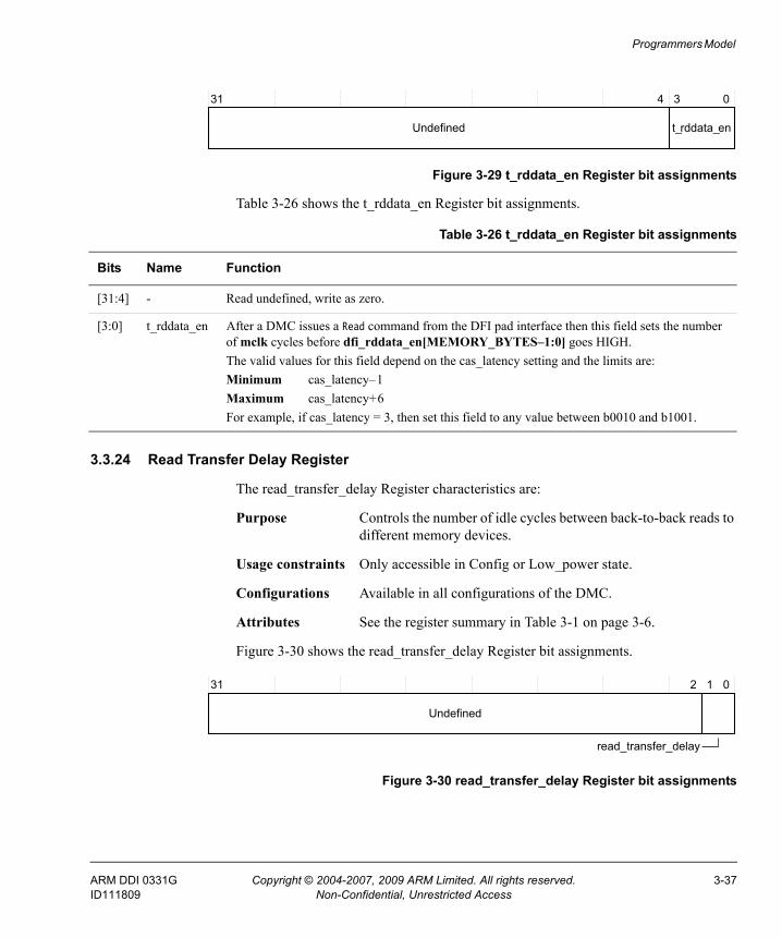
Programmers Model
Figure 3-29 t_rddata_en Register bit assignments
Table 3-26 shows the t_rddata_en Register bit assignments.
3.3.24 Read Transfer Delay Register
The read_transfer_delay Register characteristics are:
Purpose Controls the number of idle cycles between back-to-back reads to different memory devices.
Usage constraints Only accessible in Config or Low_power state.
Configurations Available in all configurations of the DMC.
Attributes See the register summary in Table 3-1 on page 3-6.
Figure 3-30 shows the read_transfer_delay Register bit assignments.
Figure 3-30 read_transfer_delay Register bit assignments
Undefined
31 4 3 0
t_rddata_en
Table 3-26 t_rddata_en Register bit assignments
Bits Name Function
[31:4] - Read undefined, write as zero.
[3:0] t_rddata_en After a DMC issues a Read command from the DFI pad interface then this field sets the number of mclk cycles before dfi_rddata_en[MEMORY_BYTES–1:0] goes HIGH.The valid values for this field depend on the cas_latency setting and the limits are:Minimum cas_latency–1Maximum cas_latency+6For example, if cas_latency = 3, then set this field to any value between b0010 and b1001.
Undefined
31 2 1 0
read_transfer_delay
ARM DDI 0331G Copyright © 2004-2007, 2009 ARM Limited. All rights reserved. 3-37ID111809 Non-Confidential, Unrestricted Access
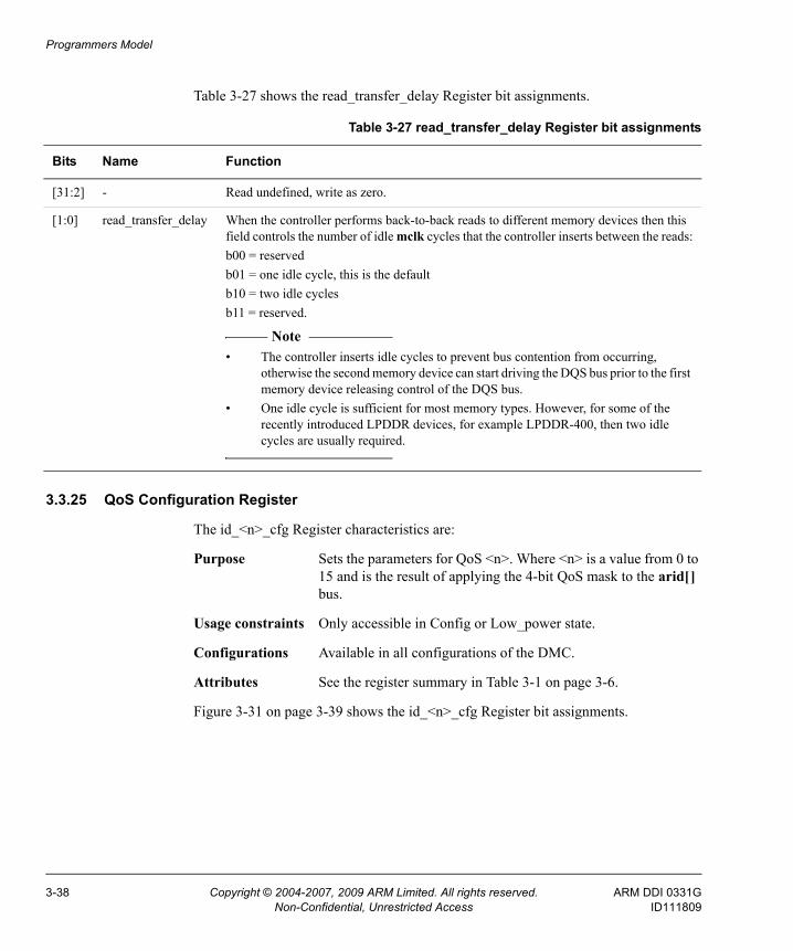
Programmers Model
Table 3-27 shows the read_transfer_delay Register bit assignments.
3.3.25 QoS Configuration Register
The id_<n>_cfg Register characteristics are:
Purpose Sets the parameters for QoS <n>. Where <n> is a value from 0 to 15 and is the result of applying the 4-bit QoS mask to the arid[] bus.
Usage constraints Only accessible in Config or Low_power state.
Configurations Available in all configurations of the DMC.
Attributes See the register summary in Table 3-1 on page 3-6.
Figure 3-31 on page 3-39 shows the id_<n>_cfg Register bit assignments.
Table 3-27 read_transfer_delay Register bit assignments
Bits Name Function
[31:2] - Read undefined, write as zero.
[1:0] read_transfer_delay When the controller performs back-to-back reads to different memory devices then this field controls the number of idle mclk cycles that the controller inserts between the reads:b00 = reservedb01 = one idle cycle, this is the defaultb10 = two idle cyclesb11 = reserved.
Note • The controller inserts idle cycles to prevent bus contention from occurring,
otherwise the second memory device can start driving the DQS bus prior to the first memory device releasing control of the DQS bus.
• One idle cycle is sufficient for most memory types. However, for some of the recently introduced LPDDR devices, for example LPDDR-400, then two idle cycles are usually required.
3-38 Copyright © 2004-2007, 2009 ARM Limited. All rights reserved. ARM DDI 0331GNon-Confidential, Unrestricted Access ID111809
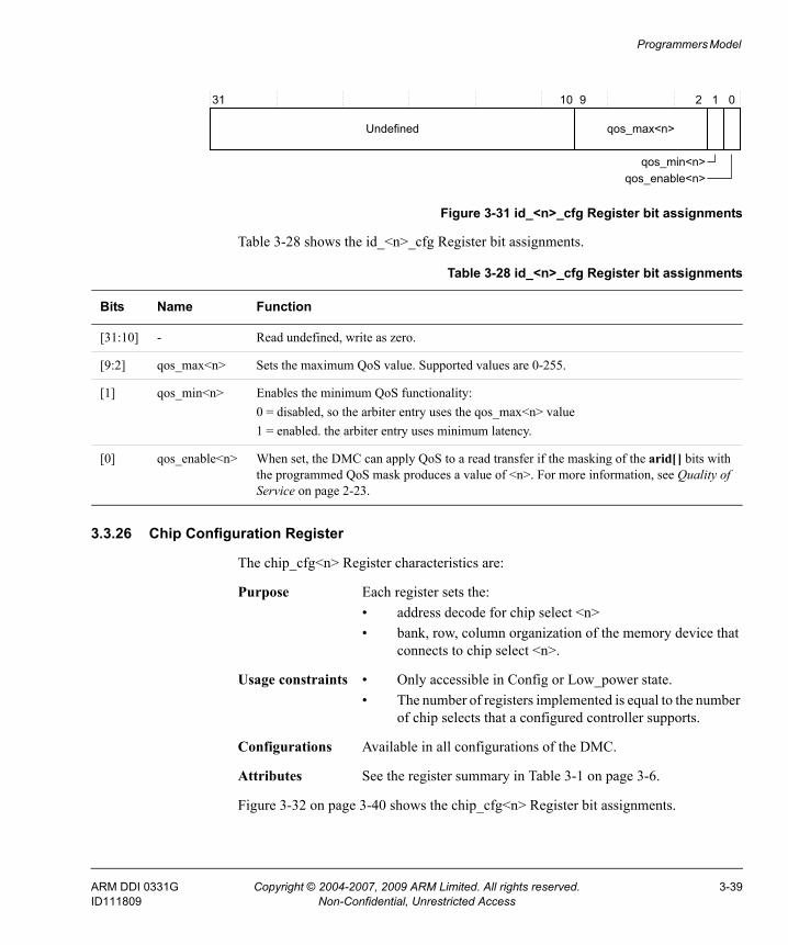
Programmers Model
Figure 3-31 id_<n>_cfg Register bit assignments
Table 3-28 shows the id_<n>_cfg Register bit assignments.
3.3.26 Chip Configuration Register
The chip_cfg<n> Register characteristics are:
Purpose Each register sets the:• address decode for chip select <n>• bank, row, column organization of the memory device that
connects to chip select <n>.
Usage constraints • Only accessible in Config or Low_power state.• The number of registers implemented is equal to the number
of chip selects that a configured controller supports.
Configurations Available in all configurations of the DMC.
Attributes See the register summary in Table 3-1 on page 3-6.
Figure 3-32 on page 3-40 shows the chip_cfg<n> Register bit assignments.
31 9 1 0
Undefined qos_max<n>
qos_enable<n>
10 2
qos_min<n>
Table 3-28 id_<n>_cfg Register bit assignments
Bits Name Function
[31:10] - Read undefined, write as zero.
[9:2] qos_max<n> Sets the maximum QoS value. Supported values are 0-255.
[1] qos_min<n> Enables the minimum QoS functionality:0 = disabled, so the arbiter entry uses the qos_max<n> value1 = enabled. the arbiter entry uses minimum latency.
[0] qos_enable<n> When set, the DMC can apply QoS to a read transfer if the masking of the arid[] bits with the programmed QoS mask produces a value of <n>. For more information, see Quality of Service on page 2-23.
ARM DDI 0331G Copyright © 2004-2007, 2009 ARM Limited. All rights reserved. 3-39ID111809 Non-Confidential, Unrestricted Access
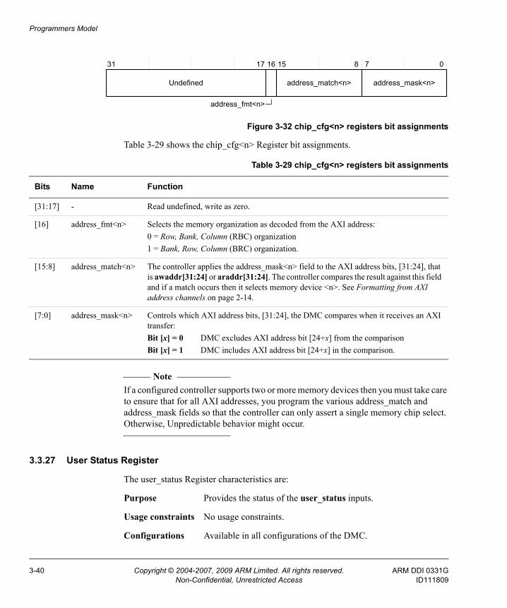
Programmers Model
Figure 3-32 chip_cfg<n> registers bit assignments
Table 3-29 shows the chip_cfg<n> Register bit assignments.
Note If a configured controller supports two or more memory devices then you must take care to ensure that for all AXI addresses, you program the various address_match and address_mask fields so that the controller can only assert a single memory chip select. Otherwise, Unpredictable behavior might occur.
3.3.27 User Status Register
The user_status Register characteristics are:
Purpose Provides the status of the user_status inputs.
Usage constraints No usage constraints.
Configurations Available in all configurations of the DMC.
31 17 16 15 8 7 0
address_fmt<n>
Undefined address_mask<n>address_match<n>
Table 3-29 chip_cfg<n> registers bit assignments
Bits Name Function
[31:17] - Read undefined, write as zero.
[16] address_fmt<n> Selects the memory organization as decoded from the AXI address:0 = Row, Bank, Column (RBC) organization1 = Bank, Row, Column (BRC) organization.
[15:8] address_match<n> The controller applies the address_mask<n> field to the AXI address bits, [31:24], that is awaddr[31:24] or araddr[31:24]. The controller compares the result against this field and if a match occurs then it selects memory device <n>. See Formatting from AXI address channels on page 2-14.
[7:0] address_mask<n> Controls which AXI address bits, [31:24], the DMC compares when it receives an AXI transfer:Bit [x] = 0 DMC excludes AXI address bit [24+x] from the comparisonBit [x] = 1 DMC includes AXI address bit [24+x] in the comparison.
3-40 Copyright © 2004-2007, 2009 ARM Limited. All rights reserved. ARM DDI 0331GNon-Confidential, Unrestricted Access ID111809
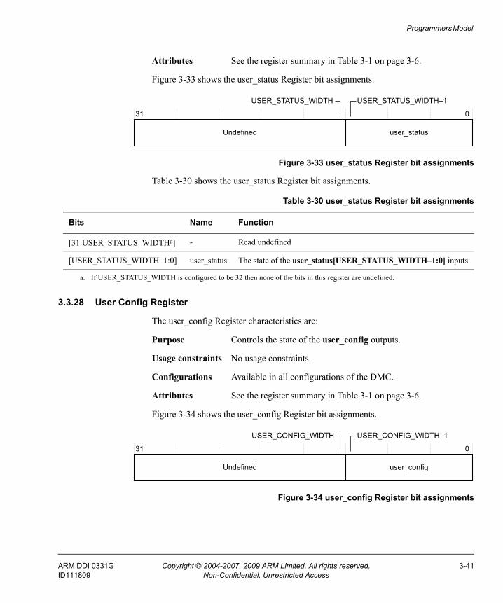
Programmers Model
Attributes See the register summary in Table 3-1 on page 3-6.
Figure 3-33 shows the user_status Register bit assignments.
Figure 3-33 user_status Register bit assignments
Table 3-30 shows the user_status Register bit assignments.
3.3.28 User Config Register
The user_config Register characteristics are:
Purpose Controls the state of the user_config outputs.
Usage constraints No usage constraints.
Configurations Available in all configurations of the DMC.
Attributes See the register summary in Table 3-1 on page 3-6.
Figure 3-34 shows the user_config Register bit assignments.
Figure 3-34 user_config Register bit assignments
user_status
31 0
USER_STATUS_WIDTH–1USER_STATUS_WIDTH
Undefined
Table 3-30 user_status Register bit assignments
Bits Name Function
[31:USER_STATUS_WIDTHa] - Read undefined
[USER_STATUS_WIDTH–1:0] user_status The state of the user_status[USER_STATUS_WIDTH–1:0] inputs
a. If USER_STATUS_WIDTH is configured to be 32 then none of the bits in this register are undefined.
user_config
31 0
USER_CONFIG_WIDTH–1USER_CONFIG_WIDTH
Undefined
ARM DDI 0331G Copyright © 2004-2007, 2009 ARM Limited. All rights reserved. 3-41ID111809 Non-Confidential, Unrestricted Access
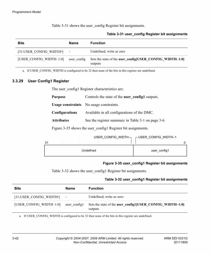
Programmers Model
Table 3-31 shows the user_config Register bit assignments.
3.3.29 User Config1 Register
The user_config1 Register characteristics are:
Purpose Controls the state of the user_config1 outputs.
Usage constraints No usage constraints.
Configurations Available in all configurations of the DMC.
Attributes See the register summary in Table 3-1 on page 3-6.
Figure 3-35 shows the user_config1 Register bit assignments.
Figure 3-35 user_config1 Register bit assignments
Table 3-32 shows the user_config1 Register bit assignments.
Table 3-31 user_config Register bit assignments
Bits Name Function
[31:USER_CONFIG_WIDTHa] - Undefined, write as zero
[USER_CONFIG_WIDTH–1:0] user_config Sets the state of the user_config[USER_CONFIG_WIDTH–1:0] outputs
a. If USER_CONFIG_WIDTH is configured to be 32 then none of the bits in this register are undefined.
user_config1
31 0
USER_CONFIG_WIDTH–1USER_CONFIG_WIDTH
Undefined
Table 3-32 user_config1 Register bit assignments
Bits Name Function
[31:USER_CONFIG_WIDTHa] - Undefined, write as zero
[USER_CONFIG_WIDTH–1:0] user_config1 Sets the state of the user_config1[USER_CONFIG_WIDTH–1:0] outputs
a. If USER_CONFIG_WIDTH is configured to be 32 then none of the bits in this register are undefined.
3-42 Copyright © 2004-2007, 2009 ARM Limited. All rights reserved. ARM DDI 0331GNon-Confidential, Unrestricted Access ID111809
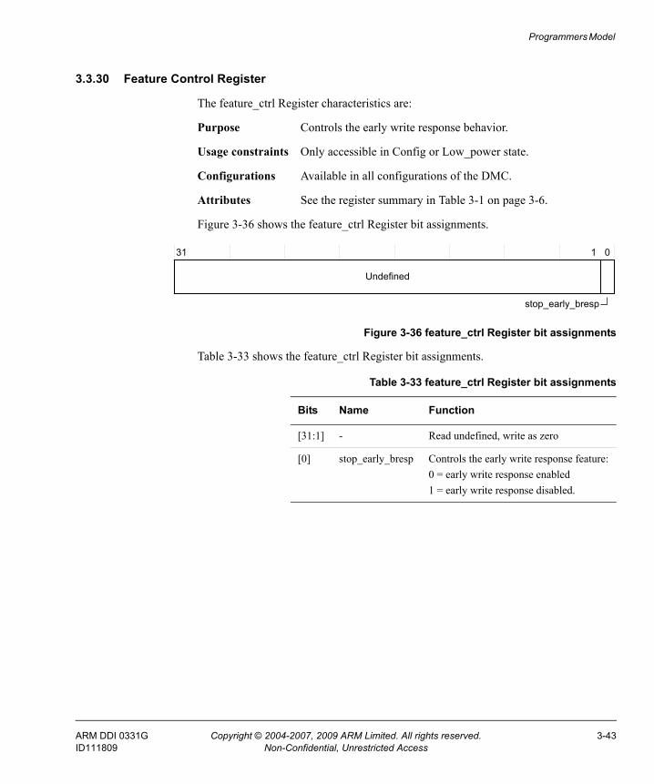
Programmers Model
3.3.30 Feature Control Register
The feature_ctrl Register characteristics are:
Purpose Controls the early write response behavior.
Usage constraints Only accessible in Config or Low_power state.
Configurations Available in all configurations of the DMC.
Attributes See the register summary in Table 3-1 on page 3-6.
Figure 3-36 shows the feature_ctrl Register bit assignments.
Figure 3-36 feature_ctrl Register bit assignments
Table 3-33 shows the feature_ctrl Register bit assignments.
31 0
Undefined
1
stop_early_bresp
Table 3-33 feature_ctrl Register bit assignments
Bits Name Function
[31:1] - Read undefined, write as zero
[0] stop_early_bresp Controls the early write response feature:0 = early write response enabled1 = early write response disabled.
ARM DDI 0331G Copyright © 2004-2007, 2009 ARM Limited. All rights reserved. 3-43ID111809 Non-Confidential, Unrestricted Access
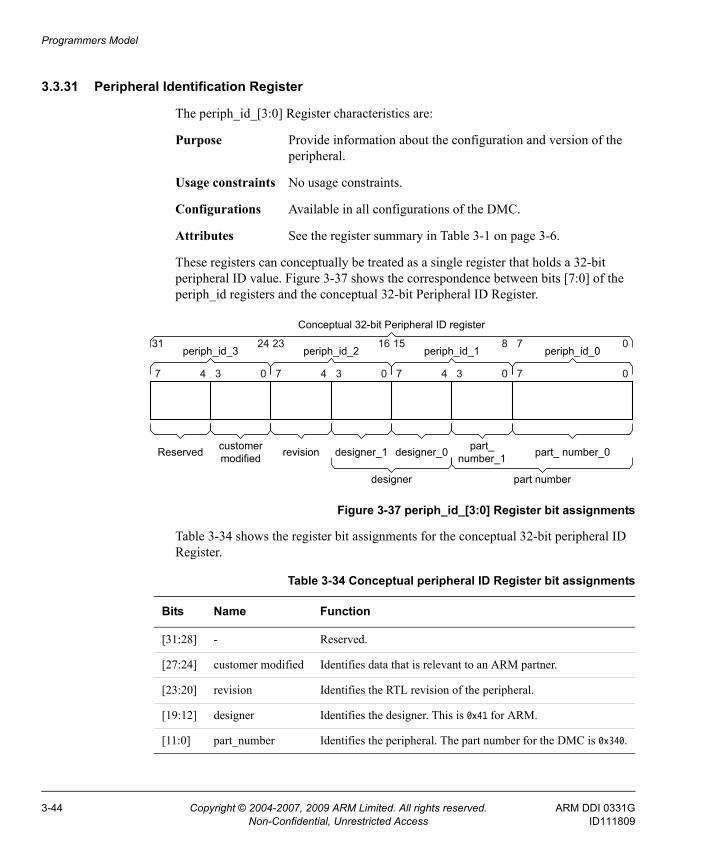
Programmers Model
3.3.31 Peripheral Identification Register
The periph_id_[3:0] Register characteristics are:
Purpose Provide information about the configuration and version of the peripheral.
Usage constraints No usage constraints.
Configurations Available in all configurations of the DMC.
Attributes See the register summary in Table 3-1 on page 3-6.
These registers can conceptually be treated as a single register that holds a 32-bit peripheral ID value. Figure 3-37 shows the correspondence between bits [7:0] of the periph_id registers and the conceptual 32-bit Peripheral ID Register.
Figure 3-37 periph_id_[3:0] Register bit assignments
Table 3-34 shows the register bit assignments for the conceptual 32-bit peripheral ID Register.
31 24 23 16 15 8 7 0
7 0 7 4 3 0 7 4 3 0 7 0
periph_id_0
customer modified revision
designer part number
designer_1 designer_0 part_ number_1 part_ number_0Reserved
periph_id_1periph_id_2periph_id_3
Conceptual 32-bit Peripheral ID register
4 3
Table 3-34 Conceptual peripheral ID Register bit assignments
Bits Name Function
[31:28] - Reserved.
[27:24] customer modified Identifies data that is relevant to an ARM partner.
[23:20] revision Identifies the RTL revision of the peripheral.
[19:12] designer Identifies the designer. This is 0x41 for ARM.
[11:0] part_number Identifies the peripheral. The part number for the DMC is 0x340.
3-44 Copyright © 2004-2007, 2009 ARM Limited. All rights reserved. ARM DDI 0331GNon-Confidential, Unrestricted Access ID111809
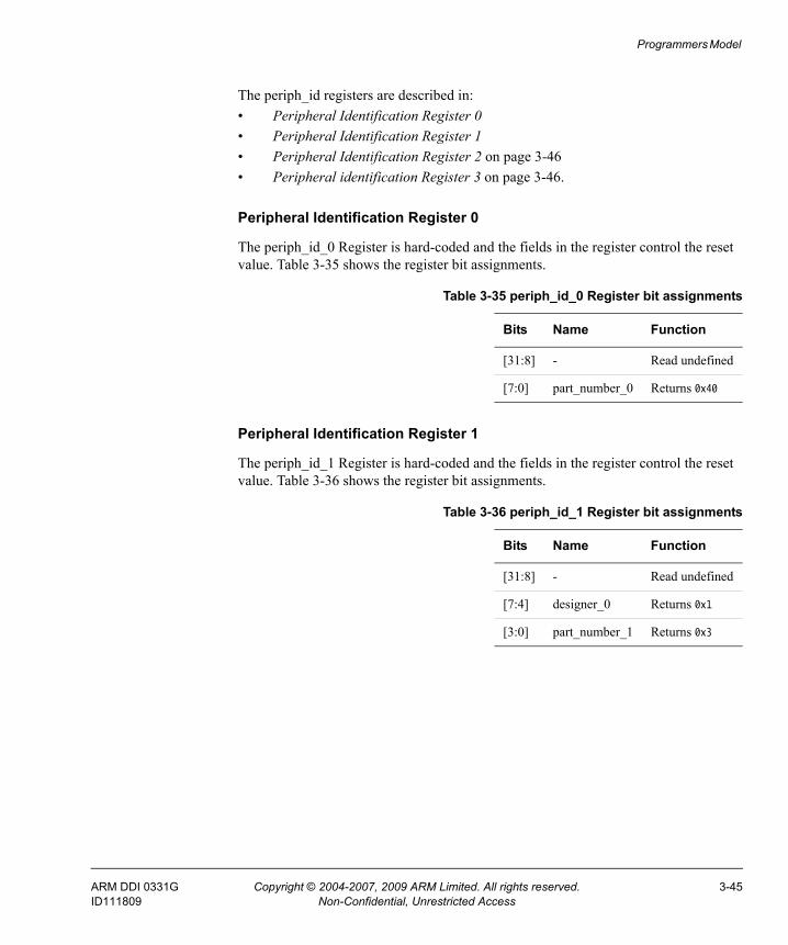
Programmers Model
The periph_id registers are described in:• Peripheral Identification Register 0• Peripheral Identification Register 1• Peripheral Identification Register 2 on page 3-46• Peripheral identification Register 3 on page 3-46.
Peripheral Identification Register 0
The periph_id_0 Register is hard-coded and the fields in the register control the reset value. Table 3-35 shows the register bit assignments.
Peripheral Identification Register 1
The periph_id_1 Register is hard-coded and the fields in the register control the reset value. Table 3-36 shows the register bit assignments.
Table 3-35 periph_id_0 Register bit assignments
Bits Name Function
[31:8] - Read undefined
[7:0] part_number_0 Returns 0x40
Table 3-36 periph_id_1 Register bit assignments
Bits Name Function
[31:8] - Read undefined
[7:4] designer_0 Returns 0x1
[3:0] part_number_1 Returns 0x3
ARM DDI 0331G Copyright © 2004-2007, 2009 ARM Limited. All rights reserved. 3-45ID111809 Non-Confidential, Unrestricted Access
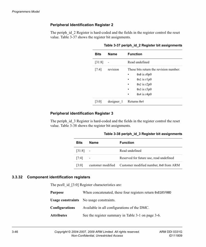
Programmers Model
Peripheral Identification Register 2
The periph_id_2 Register is hard-coded and the fields in the register control the reset value. Table 3-37 shows the register bit assignments.
Peripheral identification Register 3
The periph_id_3 Register is hard-coded and the fields in the register control the reset value. Table 3-38 shows the register bit assignments.
3.3.32 Component identification registers
The pcell_id_[3:0] Register characteristics are:
Purpose When concatenated, these four registers return 0xB105F00D
Usage constraints No usage constraints.
Configurations Available in all configurations of the DMC.
Attributes See the register summary in Table 3-1 on page 3-6.
Table 3-37 periph_id_2 Register bit assignments
Bits Name Function
[31:8] - Read undefined
[7:4] revision These bits return the revision number:• 0x0 is r0p0• 0x1 is r1p0• 0x2 is r2p0• 0x3 is r3p0• 0x4 is r4p0
[3:0] designer_1 Returns 0x4
Table 3-38 periph_id_3 Register bit assignments
Bits Name Function
[31:8] - Read undefined
[7:4] - Reserved for future use, read undefined
[3:0] customer modified Customer modified number, 0x0 from ARM
3-46 Copyright © 2004-2007, 2009 ARM Limited. All rights reserved. ARM DDI 0331GNon-Confidential, Unrestricted Access ID111809
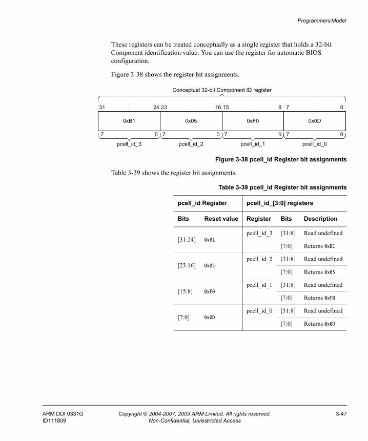
Programmers Model
These registers can be treated conceptually as a single register that holds a 32-bit Component identification value. You can use the register for automatic BIOS configuration.
Figure 3-38 shows the register bit assignments.
Figure 3-38 pcell_id Register bit assignments
Table 3-39 shows the register bit assignments.
7 0 7 0 7 0 7 0
Conceptual 32-bit Component ID register
31 24 23 16 15 8 7 0
0x0D0xF00x050xB1
pcell_id_3 pcell_id_2 pcell_id_1 pcell_id_0
Table 3-39 pcell_id Register bit assignments
pcell_id Register pcell_id_[3:0] registers
Bits Reset value Register Bits Description
[31:24] 0xB1pcell_id_3 [31:8] Read undefined
[7:0] Returns 0xB1
[23:16] 0x05pcell_id_2 [31:8] Read undefined
[7:0] Returns 0x05
[15:8] 0xF0pcell_id_1 [31:8] Read undefined
[7:0] Returns 0xF0
[7:0] 0x0Dpcell_id_0 [31:8] Read undefined
[7:0] Returns 0x0D
ARM DDI 0331G Copyright © 2004-2007, 2009 ARM Limited. All rights reserved. 3-47ID111809 Non-Confidential, Unrestricted Access

Programmers Model
3-48 Copyright © 2004-2007, 2009 ARM Limited. All rights reserved. ARM DDI 0331GNon-Confidential, Unrestricted Access ID111809
Chapter 4 Programmers Model for Test
This chapter describes the additional logic for functional verification and production testing. It contains the following section:• Integration test registers on page 4-2.
ARM DDI 0331G Copyright © 2004-2007, 2009 ARM Limited. All rights reserved. 4-1ID111809 Non-Confidential, Unrestricted Access
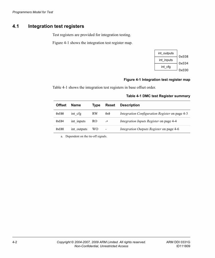
Programmers Model for Test
4.1 Integration test registersTest registers are provided for integration testing.
Figure 4-1 shows the integration test register map.
Figure 4-1 Integration test register map
Table 4-1 shows the integration test registers in base offset order.
int_cfg0xE00
0xE04int_inputs
0xE08int_outputs
Table 4-1 DMC test Register summary
Offset Name Type Reset Description
0xE00 int_cfg RW 0x0 Integration Configuration Register on page 4-3
0xE04 int_inputs RO -a
a. Dependent on the tie-off signals.
Integration Inputs Register on page 4-4
0xE08 int_outputs WO - Integration Outputs Register on page 4-6
4-2 Copyright © 2004-2007, 2009 ARM Limited. All rights reserved. ARM DDI 0331GNon-Confidential, Unrestricted Access ID111809
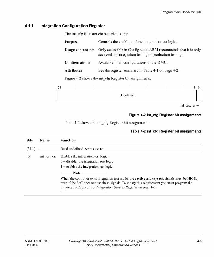
Programmers Model for Test
4.1.1 Integration Configuration Register
The int_cfg Register characteristics are:
Purpose Controls the enabling of the integration test logic.
Usage constraints Only accessible in Config state. ARM recommends that it is only accessed for integration testing or production testing.
Configurations Available in all configurations of the DMC.
Attributes See the register summary in Table 4-1 on page 4-2.
Figure 4-2 shows the int_cfg Register bit assignments.
Figure 4-2 int_cfg Register bit assignments
Table 4-2 shows the int_cfg Register bit assignments.
31 1 0
Undefined
int_test_en
Table 4-2 int_cfg Register bit assignments
Bits Name Function
[31:1] - Read undefined, write as zero.
[0] int_test_en Enables the integration test logic:0 = disables the integration test logic1 = enables the integration test logic.
Note When the controller exits integration test mode, the cactive and csysack signals must be HIGH, even if the SoC does not use these signals. To satisfy this requirement you must program the int_outputs Register, see Integration Outputs Register on page 4-6.
ARM DDI 0331G Copyright © 2004-2007, 2009 ARM Limited. All rights reserved. 4-3ID111809 Non-Confidential, Unrestricted Access
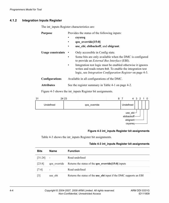
Programmers Model for Test
4.1.2 Integration Inputs Register
The int_inputs Register characteristics are:
Purpose Provides the status of the following inputs:• csysreq• qos_override[15:0]• use_ebi, ebibackoff, and ebigrant.
Usage constraints • Only accessible in Config state.• Some bits are only available when the DMC is configured
to provide an External Bus Interface (EBI).• Integration test logic must be enabled otherwise it ignores
writes and reads return 0x0. To enable the integration test logic, see Integration Configuration Register on page 4-3.
Configurations Available in all configurations of the DMC.
Attributes See the register summary in Table 4-1 on page 4-2.
Figure 4-3 shows the int_inputs Register bit assignments.
Figure 4-3 int_inputs Register bit assignments
Table 4-3 shows the int_inputs Register bit assignments.
Undefined qos_override
use_ebiebibackoff
ebigrantcsysreq
31 24 23 8 7 4 3 2 1 0
Undefined
Table 4-3 int_inputs Register bit assignments
Bits Name Function
[31:24] - Read undefined
[23:8] qos_override Returns the status of the qos_override[15:0] inputs
[7:4] - Read undefined
[3] use_ebi Returns the status of the use_ebi input if the DMC supports an EBI
4-4 Copyright © 2004-2007, 2009 ARM Limited. All rights reserved. ARM DDI 0331GNon-Confidential, Unrestricted Access ID111809
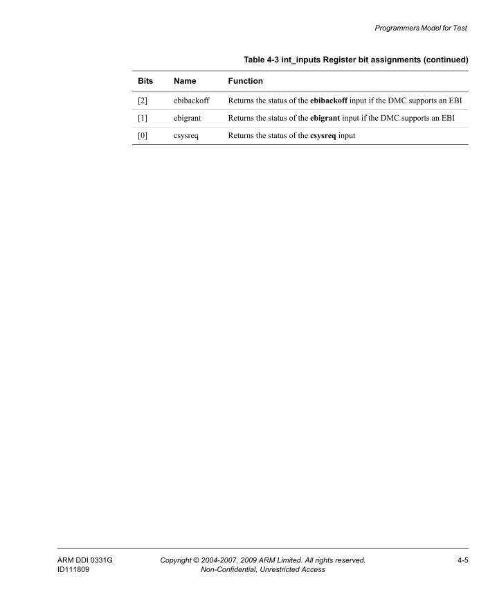
Programmers Model for Test
[2] ebibackoff Returns the status of the ebibackoff input if the DMC supports an EBI
[1] ebigrant Returns the status of the ebigrant input if the DMC supports an EBI
[0] csysreq Returns the status of the csysreq input
Table 4-3 int_inputs Register bit assignments (continued)
Bits Name Function
ARM DDI 0331G Copyright © 2004-2007, 2009 ARM Limited. All rights reserved. 4-5ID111809 Non-Confidential, Unrestricted Access
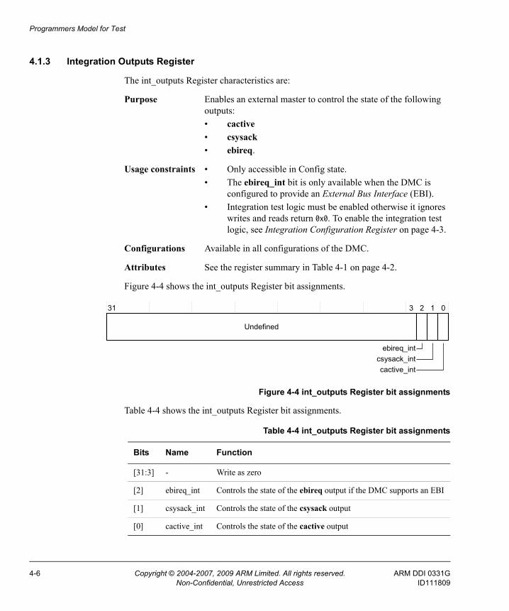
Programmers Model for Test
4.1.3 Integration Outputs Register
The int_outputs Register characteristics are:
Purpose Enables an external master to control the state of the following outputs:• cactive• csysack• ebireq.
Usage constraints • Only accessible in Config state.• The ebireq_int bit is only available when the DMC is
configured to provide an External Bus Interface (EBI).• Integration test logic must be enabled otherwise it ignores
writes and reads return 0x0. To enable the integration test logic, see Integration Configuration Register on page 4-3.
Configurations Available in all configurations of the DMC.
Attributes See the register summary in Table 4-1 on page 4-2.
Figure 4-4 shows the int_outputs Register bit assignments.
Figure 4-4 int_outputs Register bit assignments
Table 4-4 shows the int_outputs Register bit assignments.
31 1 0
Undefined
ebireq_intcsysack_intcactive_int
3 2
Table 4-4 int_outputs Register bit assignments
Bits Name Function
[31:3] - Write as zero
[2] ebireq_int Controls the state of the ebireq output if the DMC supports an EBI
[1] csysack_int Controls the state of the csysack output
[0] cactive_int Controls the state of the cactive output
4-6 Copyright © 2004-2007, 2009 ARM Limited. All rights reserved. ARM DDI 0331GNon-Confidential, Unrestricted Access ID111809

Chapter 5 Device Driver
This chapter introduces the device driver operation. It contains the following section:• Sample device driver on page 5-2
ARM DDI 0331G Copyright © 2004-2007, 2009 ARM Limited. All rights reserved. 5-1ID111809 Non-Confidential, Unrestricted Access
Device Driver
5.1 Sample device driverThe following sections describe about the operation sequence of the device driver:• Memory controller initialization• Memory device initialization on page 5-3• Memory state control and status on page 5-4.
5.1.1 Memory controller initialization
Initialization involves the following steps:
1. Initialization of the timing control registers. See DMC configuration register map on page 3-3. Depending on the configuration of the controller then you might need to initialize the following register fields:• cas latency• cas_half_cycle• t_dqss• t_mrd• t_ras• t_rc• t_rcd• schedule_rcd • t_rfc• schedule_rfc• t_rp• schedule_rp• t_rrd• t_wr• t_wtr• t_xp• t_xsr• t_esr• read_transfer_delay• update_type and t_rddata_en for DFI configurations.
2. Initialization of memory configuration. See Memory Configuration Register on page 3-15. Example of Register fields that needs to be initialized are:• column_bits• row_bits• ap_bit
5-2 Copyright © 2004-2007, 2009 ARM Limited. All rights reserved. ARM DDI 0331GNon-Confidential, Unrestricted Access ID111809
Device Driver
• power_dwn_prd• auto_power_down• stop_mem_clock• memory_burst• qos_master_bits.
3. Program the refresh period in the refresh_prd Register. See Refresh Period Register on page 3-19.
4. Program the configuration of the external memory devices in to the chip_cfg<n> registers. See Chip Configuration Register on page 3-39.
5. Program the QoS settings you require in to the id_<n>_cfg registers. See QoS Configuration Register on page 3-38.
Controller initialization on page 2-35 shows a DMC initialization example.
5.1.2 Memory device initialization
Memory initialization involves writing to the direct_cmd Register. See Direct Command Register on page 3-13. To initialize the mode registers in a memory device you must perform multiple writes to the direct_cmd Register, so that the controller generates the necessary sequence of commands that your specified memory requires.
A typical memory initialization sequence for each memory device is:
1. Program the direct_cmd Register so that the DMC issues a PRECHARGEALL command.
2. Set Extended Mode Register.
3. Set Mode Register.
4. Program the direct_cmd Register so that the DMC issues a PRECHARGEALL command.
5. Program the direct_cmd Register so that the DMC issues two AUTO REFRESH commands.
LPDDR device initialization on page 2-36 shows a memory initialization example.
ARM DDI 0331G Copyright © 2004-2007, 2009 ARM Limited. All rights reserved. 5-3ID111809 Non-Confidential, Unrestricted Access
Device Driver
5.1.3 Memory state control and status
You can change the state of the controller by programming the memc_cmd Register. See memc_cmd Register bit assignments on page 3-12. A typical sequence is:
1. Read the memc_status Register to check the status of the controller. See Memory Controller Status Register on page 3-9.
2. When the controller is in the Config state you can initialize the controller as Memory controller initialization on page 5-2 describes.
3. Program the memc_cmd Register with the Go command to move the controller to the Ready state.
Initialize memory as described in Memory device initialization on page 5-3.
5-4 Copyright © 2004-2007, 2009 ARM Limited. All rights reserved. ARM DDI 0331GNon-Confidential, Unrestricted Access ID111809
Appendix A Signal Descriptions
This chapter describes the AMBA AXI, AMBA APB, and module-specific non-AMBA signals that the DMC provides. It contains the following sections:• Clock and reset signals on page A-2• Miscellaneous signals on page A-3• AXI signals on page A-6• APB signals on page A-10• Pad interface signals on page A-11• EBI signals on page A-14.
ARM DDI 0331G Copyright © 2004-2007, 2009 ARM Limited. All rights reserved. A-1ID111809 Non-Confidential, Unrestricted Access
Signal Descriptions
A.1 Clock and reset signalsTable A-1 shows the clock and reset signals.
Table A-1 Clock and reset signals
Signal Type Source Description
aclk Input Clock source Clock for the aclk domain.
aresetn Input Reset source aclk domain reset signal. This signal is active LOW.
cclken Input Bus clock Clock enable for the AXI low-power interface.
mclk Input Clock source Clock for mclk domain.
mclkna
a. This signal is not available when the DMC is configured to implement a DDR PHY Interface (DFI) pad interface.
Input Clock source Mandatory clock for pad interface block.
mclkx2a Input Clock source Optional clock for pad interface block.
mclkx2na Input Clock source Optional clock for pad interface block.
mresetn Input Reset source Reset for mclk domain. This signal is active LOW.
pclken Input Bus clock Clock enable for the APB interface.
A-2 Copyright © 2004-2007, 2009 ARM Limited. All rights reserved. ARM DDI 0331GNon-Confidential, Unrestricted Access ID111809
Signal Descriptions
A.2 Miscellaneous signalsThis section describes the following miscellaneous signals:• QoS• Tie-offs• User signals on page A-5• Scan test on page A-5.
A.2.1 QoS
Table A-2 shows the QoS signal.
A.2.2 Tie-offs
Table A-3 shows the tie-off signals.
Table A-2 QoS signal
Signal Type Source Description
qos_override[15:0] Input External control logic
When one or more bits are HIGH, coincident with arvalid and arready, and when the arid match bits are equivalent to the qos_override bit(s), then the QoS for the read access is forced to minimum latency. For more information, see Quality of Service on page 2-23.
Table A-3 Tie-off signals
Signal Type Source Description
a_gt_m_sync Input Tie-off When aresetn is deasserted, the state of this signal sets the value of the clock_cfg [1] bit in the memory_cfg2 Register. See Memory Configuration 2 Register on page 3-30.Set this signal HIGH if aclk is greater than mclk and is synchronous.
cke_init Input Tie-off When aresetn is deasserted, the state of this signal sets the value of the cke_init bit in the memory_cfg2 Register. See Memory Configuration 2 Register on page 3-30.This signal is only available when the DMC is configured to provide a legacy pad interface.
dqm_init Input Tie-off When aresetn is deasserted, the state of this signal sets the value of the dqm_init bit in the memory_cfg2 Register. See Memory Configuration 2 Register on page 3-30.This signal is only available when the DMC is configured to provide a legacy pad interface.
ARM DDI 0331G Copyright © 2004-2007, 2009 ARM Limited. All rights reserved. A-3ID111809 Non-Confidential, Unrestricted Access
Signal Descriptions
memory_width[1:0] Input Tie-off When aresetn is deasserted, the state of this signal sets the value of the memory_width field in the memory_cfg2 Register. See Memory Configuration 2 Register on page 3-30.
memory_type[2:0] Input Tie-off When aresetn is deasserted, the state of this signal sets the value of the memory_protocol field in the memory_cfg2 Register. See Memory Configuration 2 Register on page 3-30.You must set this signal to select a memory protocol that the configured DMC supports. The memory_protocol field shows the possible bit encodings, see Memory Configuration 2 Register on page 3-30.
read_delay[1:0] Input Tie-off When aresetn is deasserted, the state of this signal sets the value of the read_delay field in the memory_cfg2 Register. See Memory Configuration 2 Register on page 3-30.
sync Input Tie-off When aresetn is deasserted, the state of this signal sets the value of the clock_cfg [0] bit in the memory_cfg2 Register. See Memory Configuration 2 Register on page 3-30.Set this signal HIGH if aclk is synchronous to mclk.Set this signal LOW if aclk is asynchronous to mclk.
use_ebia Input Tie-off Set this signal HIGH if the memory interface of the DMC connects to a PrimeCell External Bus Interface (PL220).
a. This signal is not present when the DMC is configured to implement a DFI pad interface.
Table A-3 Tie-off signals (continued)
Signal Type Source Description
A-4 Copyright © 2004-2007, 2009 ARM Limited. All rights reserved. ARM DDI 0331GNon-Confidential, Unrestricted Access ID111809
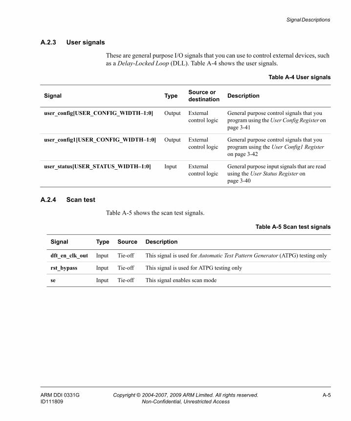
Signal Descriptions
A.2.3 User signals
These are general purpose I/O signals that you can use to control external devices, such as a Delay-Locked Loop (DLL). Table A-4 shows the user signals.
A.2.4 Scan test
Table A-5 shows the scan test signals.
Table A-4 User signals
Signal Type Source or destination Description
user_config[USER_CONFIG_WIDTH–1:0] Output External control logic
General purpose control signals that you program using the User Config Register on page 3-41
user_config1[USER_CONFIG_WIDTH–1:0] Output External control logic
General purpose control signals that you program using the User Config1 Register on page 3-42
user_status[USER_STATUS_WIDTH–1:0] Input External control logic
General purpose input signals that are read using the User Status Register on page 3-40
Table A-5 Scan test signals
Signal Type Source Description
dft_en_clk_out Input Tie-off This signal is used for Automatic Test Pattern Generator (ATPG) testing only
rst_bypass Input Tie-off This signal is used for ATPG testing only
se Input Tie-off This signal enables scan mode
ARM DDI 0331G Copyright © 2004-2007, 2009 ARM Limited. All rights reserved. A-5ID111809 Non-Confidential, Unrestricted Access
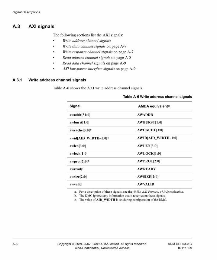
Signal Descriptions
A.3 AXI signalsThe following sections list the AXI signals:• Write address channel signals• Write data channel signals on page A-7• Write response channel signals on page A-7• Read address channel signals on page A-8• Read data channel signals on page A-9• AXI low-power interface signals on page A-9.
A.3.1 Write address channel signals
Table A-6 shows the AXI write address channel signals.
Table A-6 Write address channel signals
Signal AMBA equivalenta
a. For a description of these signals, see the AMBA AXI Protocol v1.0 Specification.
awaddr[31:0] AWADDR
awburst[1:0] AWBURST[1:0]
awcache[3:0]b
b. The DMC ignores any information that it receives on these signals.
AWCACHE[3:0]
awid[AID_WIDTH–1:0]c
c. The value of AID_WIDTH is set during configuration of the DMC.
AWID[AID_WIDTH–1:0]
awlen[3:0] AWLEN[3:0]
awlock[1:0] AWLOCK[1:0]
awprot[2:0]b AWPROT[2:0]
awready AWREADY
awsize[2:0] AWSIZE[2:0]
awvalid AWVALID
A-6 Copyright © 2004-2007, 2009 ARM Limited. All rights reserved. ARM DDI 0331GNon-Confidential, Unrestricted Access ID111809
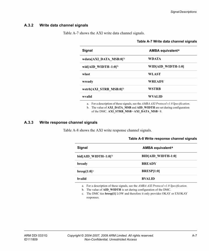
Signal Descriptions
A.3.2 Write data channel signals
Table A-7 shows the AXI write data channel signals.
A.3.3 Write response channel signals
Table A-8 shows the AXI write response channel signals.
Table A-7 Write data channel signals
Signal AMBA equivalenta
a. For a description of these signals, see the AMBA AXI Protocol v1.0 Specification.
wdata[AXI_DATA_MSB:0]b
b. The value of AXI_DATA_MSB and AID_WIDTH are set during configuration of the DMC. AXI_STRB_MSB=AXI_DATA_MSB÷8.
WDATA
wid[AID_WIDTH–1:0]b WID[AID_WIDTH-1:0]
wlast WLAST
wready WREADY
wstrb[AXI_STRB_MSB:0]b WSTRB
wvalid WVALID
Table A-8 Write response channel signals
Signal AMBA equivalenta
a. For a description of these signals, see the AMBA AXI Protocol v1.0 Specification.
bid[AID_WIDTH–1:0]b
b. The value of AID_WIDTH is set during configuration of the DMC.
BID[AID_WIDTH-1:0]
bready BREADY
bresp[1:0]c
c. The DMC ties bresp[1] LOW and therefore it only provides OKAY or EXOKAY responses.
BRESP[1:0]
bvalid BVALID
ARM DDI 0331G Copyright © 2004-2007, 2009 ARM Limited. All rights reserved. A-7ID111809 Non-Confidential, Unrestricted Access
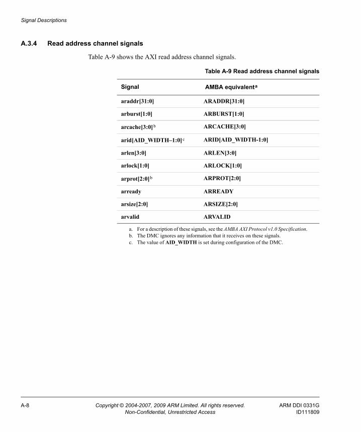
Signal Descriptions
A.3.4 Read address channel signals
Table A-9 shows the AXI read address channel signals.
Table A-9 Read address channel signals
Signal AMBA equivalenta
a. For a description of these signals, see the AMBA AXI Protocol v1.0 Specification.
araddr[31:0] ARADDR[31:0]
arburst[1:0] ARBURST[1:0]
arcache[3:0]b
b. The DMC ignores any information that it receives on these signals.
ARCACHE[3:0]
arid[AID_WIDTH–1:0]c
c. The value of AID_WIDTH is set during configuration of the DMC.
ARID[AID_WIDTH-1:0]
arlen[3:0] ARLEN[3:0]
arlock[1:0] ARLOCK[1:0]
arprot[2:0]b ARPROT[2:0]
arready ARREADY
arsize[2:0] ARSIZE[2:0]
arvalid ARVALID
A-8 Copyright © 2004-2007, 2009 ARM Limited. All rights reserved. ARM DDI 0331GNon-Confidential, Unrestricted Access ID111809
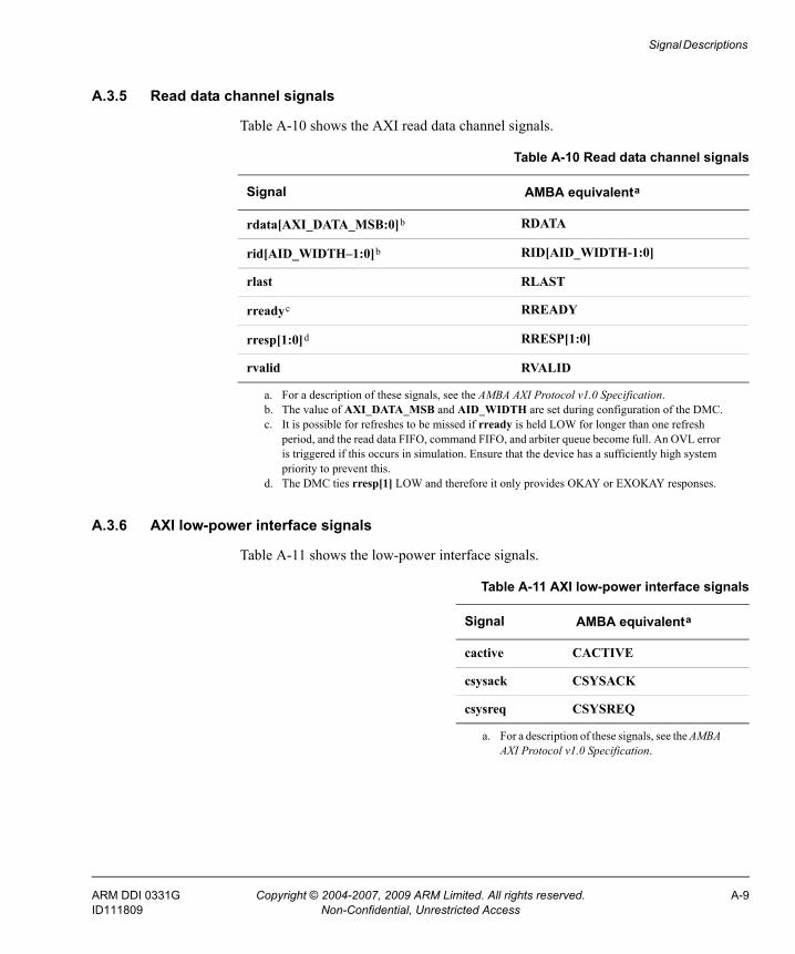
Signal Descriptions
A.3.5 Read data channel signals
Table A-10 shows the AXI read data channel signals.
A.3.6 AXI low-power interface signals
Table A-11 shows the low-power interface signals.
Table A-10 Read data channel signals
Signal AMBA equivalenta
a. For a description of these signals, see the AMBA AXI Protocol v1.0 Specification.
rdata[AXI_DATA_MSB:0]b
b. The value of AXI_DATA_MSB and AID_WIDTH are set during configuration of the DMC.
RDATA
rid[AID_WIDTH–1:0]b RID[AID_WIDTH-1:0]
rlast RLAST
rreadyc
c. It is possible for refreshes to be missed if rready is held LOW for longer than one refresh period, and the read data FIFO, command FIFO, and arbiter queue become full. An OVL error is triggered if this occurs in simulation. Ensure that the device has a sufficiently high system priority to prevent this.
RREADY
rresp[1:0]d
d. The DMC ties rresp[1] LOW and therefore it only provides OKAY or EXOKAY responses.
RRESP[1:0]
rvalid RVALID
Table A-11 AXI low-power interface signals
Signal AMBA equivalenta
a. For a description of these signals, see the AMBA AXI Protocol v1.0 Specification.
cactive CACTIVE
csysack CSYSACK
csysreq CSYSREQ
ARM DDI 0331G Copyright © 2004-2007, 2009 ARM Limited. All rights reserved. A-9ID111809 Non-Confidential, Unrestricted Access
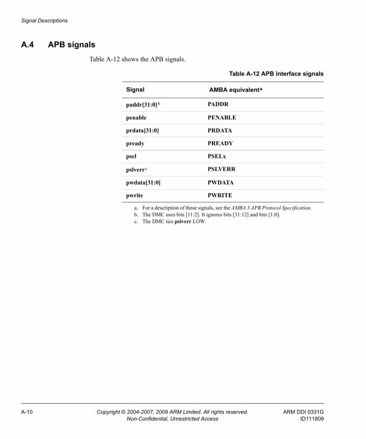
Signal Descriptions
A.4 APB signalsTable A-12 shows the APB signals.
Table A-12 APB interface signals
Signal AMBA equivalenta
a. For a description of these signals, see the AMBA 3 APB Protocol Specification.
paddr[31:0]b
b. The DMC uses bits [11:2]. It ignores bits [31:12] and bits [1:0].
PADDR
penable PENABLE
prdata[31:0] PRDATA
pready PREADY
psel PSELx
pslverrc
c. The DMC ties pslverr LOW.
PSLVERR
pwdata[31:0] PWDATA
pwrite PWRITE
A-10 Copyright © 2004-2007, 2009 ARM Limited. All rights reserved. ARM DDI 0331GNon-Confidential, Unrestricted Access ID111809
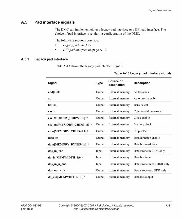
Signal Descriptions
A.5 Pad interface signalsThe DMC can implement either a legacy pad interface or a DFI pad interface. The choice of pad interface is set during configuration of the DMC.
The following sections describe:• Legacy pad interface• DFI pad interface on page A-12.
A.5.1 Legacy pad interface
Table A-13 shows the legacy pad interface signals.
Table A-13 Legacy pad interface signals
Signal Type Source or destination Description
add[15:0] Output External memory Address bus
ap Output External memory Auto precharge bit
ba[1:0] Output External memory Bank select
cas_n Output External memory Column address strobe
cke[MEMORY_CHIPS–1:0]ab Output External memory Clock enable
clk_out[MEMORY_CHIPS–1:0]b Output External memory Memory clock
cs_n[MEMORY_CHIPS–1:0]b Output External memory Chip select
data_en Output External memory Data direction enable
dqm[MEMORY_BYTES–1:0]c Output External memory Data bus mask bits
dqs_in_<n> Input External memory Data strobe in, DDR only
dq_in[MEMWIDTH–1:0]d Input External memory Data bus input
dqs_in_n_<n> Input External memory Data strobe in bar, DDR only
dqs_out_<n> Output External memory Data strobe out, DDR only
dq_out[MEMWIDTH–1:0]d Output External memory Data bus output
ARM DDI 0331G Copyright © 2004-2007, 2009 ARM Limited. All rights reserved. A-11ID111809 Non-Confidential, Unrestricted Access
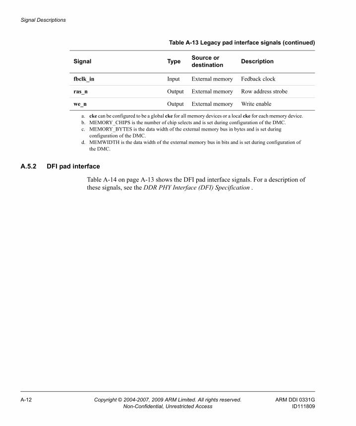
Signal Descriptions
A.5.2 DFI pad interface
Table A-14 on page A-13 shows the DFI pad interface signals. For a description of these signals, see the DDR PHY Interface (DFI) Specification .
fbclk_in Input External memory Fedback clock
ras_n Output External memory Row address strobe
we_n Output External memory Write enable
a. cke can be configured to be a global cke for all memory devices or a local cke for each memory device.b. MEMORY_CHIPS is the number of chip selects and is set during configuration of the DMC.c. MEMORY_BYTES is the data width of the external memory bus in bytes and is set during
configuration of the DMC.d. MEMWIDTH is the data width of the external memory bus in bits and is set during configuration of
the DMC.
Table A-13 Legacy pad interface signals (continued)
Signal Type Source or destination Description
A-12 Copyright © 2004-2007, 2009 ARM Limited. All rights reserved. ARM DDI 0331GNon-Confidential, Unrestricted Access ID111809
Signal Descriptions
Table A-14 DFI pad interface signals
Signal Type Source or destination
dfi_address[15:0] Output PHY device
dfi_bank[1:0] Output
dfi_cas_n Output
dfi_cke[MEMORY_CHIPS–1:0]a Output
dfi_cs_n[MEMORY_CHIPS–1:0]a Output
dfi_dram_clk_disable[MEMORY_CHIPS–1:0]b Output
dfi_init_complete Input
dfi_phyupd_ack Output
dfi_phyupd_req Input
dfi_phyupd_type[1:0] Input
dfi_ras_n Output
dfi_rddata_en[MEMORY_BYTES–1:0]b Output
dfi_rddata[MEMWIDTH–1:0]c Input
dfi_rddata_validd Input
dfi_we_n Output
dfi_wrdata_en[MEMORY_BYTES–1:0]b Output
dfi_wrdata[MEMWIDTH–1:0]c Output
dfi_wrdata_mask[MEMORY_BYTES–1:0]b Output
a. MEMORY_CHIPS is the number of chip selects and is set during configuration of the DMC.b. MEMORY_BYTES is the data width of the external memory bus in bytes and is set during
configuration of the DMC.c. MEMWIDTH is the data width of the external memory bus in bits and is set during configuration of
the DMC.
ARM DDI 0331G Copyright © 2004-2007, 2009 ARM Limited. All rights reserved. A-13ID111809 Non-Confidential, Unrestricted Access
Signal Descriptions
A.6 EBI signalsTable A-15 shows the External Bus Interface (EBI) signals.
Note The EBI is only present when the DMC is configured to implement a legacy pad interface.
Table A-15 EBI signals
Signal Type Source or destination Description
ebibackoff Input DMC External memory bus access backoff. The EBI backoff signal goes HIGH when the PrimeCell EBI (PL220) wants to remove the DMC from the memory bus so that another memory controller can be granted the memory bus.
ebigrant Input DMC External memory bus grant. This signal goes HIGH when the EBI (PL220) grants the external memory bus to the DMC.
ebireq Output External External memory bus request. The DMC sets this signal HIGH when it requests access to the memory bus.
A-14 Copyright © 2004-2007, 2009 ARM Limited. All rights reserved. ARM DDI 0331GNon-Confidential, Unrestricted Access ID111809
Appendix B Revisions
This appendix describes the technical changes between released issues of this book.
Table B-1 Differences between issue F and issue G
Change Location Affects
Added the DDR PHY Interface (DFI) pad interface feature including the DFI signals and registers
Throughout book r4p0
Updated description of the supported memory data bus widths
Supported memory widths on page 1-4 All revisions
Removed support for 64-bit SDRAMs Table 1-1 on page 1-5 r4p0
Updated AXI slave interface attributes and added read interleave depth
AXI slave interface attributes on page 2-12
All revisions
Updated bus widths for arprot, awprot, arcache, and awcache
• Figure 2-2 on page 2-4• AXI signals on page A-6
All revisions
ARM DDI 0331G Copyright © 2004-2007, 2009 ARM Limited. All rights reserved. B-1ID111809 Non-Confidential, Unrestricted Access
Revisions
Added user_config1 signals and user_config1 Register • Miscellaneous signals on page 2-18
• User Config1 Register on page 3-42
• User signals on page A-5
r4p0
Added configurable bus width for the user_status, user_config, and user_config1 signals
Throughout book r4p0
Added configurable bus width for the arid, awid, bid, rid, and wid signals
Throughout book r4p0
Added early write response feature Early BRESP on page 2-13 r4p0
Added Read After Write hazard Hazard detection on page 2-22 r4p0
Updated description of system state 11 Recommended power states on page 2-39
All revisions
Updated listing of the dynamic low-power modes operation and removed the illegal bit combinations
Table 2-7 on page 2-43 All revisions
Removed restriction of issuing the NOP command when the controller includes the NVM plug-in
• Controller management operations on page 2-18
• Deep Power-Down on page 2-46• Table 3-6 on page 3-14
r4p0
Support for moving all of the memory devices to the deep power-down mode
Deep Power-Down on page 2-46 r4p0
Added a new section TrustZone Support for DMC TrustZone technology support on page 2-48
r4p0
Added supported bit, or field, values to the timing registers Chapter 3 Programmers Model All revisions
Updated the function description for fp_time bit Table 3-7 on page 3-16 r4p0
Table B-1 Differences between issue F and issue G (continued)
Change Location Affects
B-2 Copyright © 2004-2007, 2009 ARM Limited. All rights reserved. ARM DDI 0331GNon-Confidential, Unrestricted Access ID111809
Revisions
Field names changed as follows:• from memory_banks[1:0] to banks_bit[1:0]• from memory_type to memory_support• from memory_width to max_memory_width
Memory Controller Status Register on page 3-9
r2p0
Added the combined SDR-DDR-LPDDR option to the memory_support field
r2p0
Updated description of the max_memory_width field All revisions
Updated description of the sr_enable, fp_time, and fp_enable bits
Memory Configuration Register on page 3-15
All revisions
Removed restriction of enabling the sr_enable and stop_mem_clock bits at the same time
r4p0
Updated description of the cas_half_cycle bit CAS Latency Register on page 3-19 All revisions
Updated description of the memory_width field Memory Configuration 2 Register on page 3-30
r2p0
memory_type field name changed to memory_protocol
Added the combined SDR-DDR-LPDDR option to the memory_protocol field
a_gt_m_sync bit and sync bit changed to clock_cfg field
Updated description of the memory_cfg3 Register Memory Configuration 3 Register on page 3-34
r2p0
Added the read_transfer_delay Register Read Transfer Delay Register on page 3-37
r4p0
brc_n_rbc field name changed to address_fmt Chip Configuration Register on page 3-39
r3p0
Added the feature_ctrl Register Feature Control Register on page 3-43 r4p0
Updated the most significant byte of the conceptual peripheral ID register
• Figure 3-37 on page 3-44• Table 3-34 on page 3-44
All revisions
Added requirement to set cactive and csysack HIGH when the controller exits integration test mode
Integration Configuration Register on page 4-3
All revisions
Updated register description and added an _int suffix to each bit name
Integration Outputs Register on page 4-6 All revisions
Table B-1 Differences between issue F and issue G (continued)
Change Location Affects
ARM DDI 0331G Copyright © 2004-2007, 2009 ARM Limited. All rights reserved. B-3ID111809 Non-Confidential, Unrestricted Access
Revisions
Replaced the old Device Driver section with new content Chapter 5 Device Driver r4p0
Updated description of the tie-off signals Tie-offs on page A-3 All revisions
Added note about using EBI when DFI is implemented EBI signals on page A-14 r4p0
Table B-1 Differences between issue F and issue G (continued)
Change Location Affects
B-4 Copyright © 2004-2007, 2009 ARM Limited. All rights reserved. ARM DDI 0331GNon-Confidential, Unrestricted Access ID111809
Glossary
This glossary describes some of the terms used in technical documents from ARM.
Advanced eXtensible Interface (AXI)A bus protocol that supports separate address/control and data phases, unaligned data transfers using byte strobes, burst-based transactions with only start address issued, separate read and write data channels to enable low-cost DMA, ability to issue multiple outstanding addresses, out-of-order transaction completion, and easy addition of register stages to provide timing closure.
The AXI protocol also includes optional extensions to cover signaling for low-power operation.
AXI is targeted at high performance, high clock frequency system designs and includes a number of features that make it very suitable for high speed sub-micron interconnect.
Advanced Microcontroller Bus Architecture (AMBA)A family of protocol specifications that describe a strategy for the interconnect. AMBA is the ARM open standard for on-chip buses. It is an on-chip bus specification that describes a strategy for the interconnection and management of functional blocks that make up a System-on-Chip (SoC). It aids in the development of embedded processors with one or more CPUs or signal processors and multiple peripherals. AMBA complements a reusable design methodology by defining a common backbone for SoC modules.
ARM DDI 0331G Copyright © 2004-2007, 2009 ARM Limited. All rights reserved. Glossary-1ID111809 Non-Confidential, Unrestricted Access
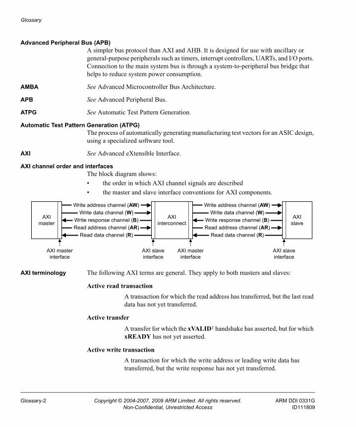
Glossary
Advanced Peripheral Bus (APB)A simpler bus protocol than AXI and AHB. It is designed for use with ancillary or general-purpose peripherals such as timers, interrupt controllers, UARTs, and I/O ports. Connection to the main system bus is through a system-to-peripheral bus bridge that helps to reduce system power consumption.
AMBA See Advanced Microcontroller Bus Architecture.
APB See Advanced Peripheral Bus.
ATPG See Automatic Test Pattern Generation.
Automatic Test Pattern Generation (ATPG)The process of automatically generating manufacturing test vectors for an ASIC design, using a specialized software tool.
AXI See Advanced eXtensible Interface.
AXI channel order and interfacesThe block diagram shows:• the order in which AXI channel signals are described• the master and slave interface conventions for AXI components.
AXI terminology The following AXI terms are general. They apply to both masters and slaves:
Active read transaction A transaction for which the read address has transferred, but the last read data has not yet transferred.
Active transfer
A transfer for which the xVALID1 handshake has asserted, but for which xREADY has not yet asserted.
Active write transaction A transaction for which the write address or leading write data has transferred, but the write response has not yet transferred.
AXI interconnect
Write address channel (AW) Write data channel (W)
Write response channel (B) Read address channel (AR)
Read data channel (R)
Write address channel (AW) Write data channel (W)
Write response channel (B) Read address channel (AR)
Read data channel (R)
AXI slave interface
AXI master interface
AXImaster
AXIslave
AXI master interface
AXI slave interface
Glossary-2 Copyright © 2004-2007, 2009 ARM Limited. All rights reserved. ARM DDI 0331GNon-Confidential, Unrestricted Access ID111809
Glossary
Completed transfer A transfer for which the xVALID/xREADY handshake is complete.
Payload The non-handshake signals in a transfer.
Transaction An entire burst of transfers, comprising an address, one or more data transfers and a response transfer (writes only).
Transmit An initiator driving the payload and asserting the relevant xVALID signal.
Transfer A single exchange of information. That is, with one xVALID/xREADY handshake.
The following AXI terms are master interface attributes. To obtain optimum performance, they must be specified for all components with an AXI master interface:
Combined issuing capability The maximum number of active transactions that a master interface can generate. It is specified for master interfaces that use combined storage for active write and read transactions. If not specified then it is assumed to be equal to the sum of the write and read issuing capabilities.
Read ID capability The maximum number of different ARID values that a master interface can generate for all active read transactions at any one time.
Read ID width The number of bits in the ARID bus.
Read issuing capability The maximum number of active read transactions that a master interface can generate.
Write ID capability The maximum number of different AWID values that a master interface can generate for all active write transactions at any one time.
1. The letter x in the signal name denotes an AXI channel as follows:AW Write address channel.W Write data channel.B Write response channel.AR Read address channel.R Read data channel.
ARM DDI 0331G Copyright © 2004-2007, 2009 ARM Limited. All rights reserved. Glossary-3ID111809 Non-Confidential, Unrestricted Access
Glossary
Write ID width The number of bits in the AWID and WID buses.
Write interleave capability The number of active write transactions for which the master interface is capable of transmitting data. This is counted from the earliest transaction.
Write issuing capability The maximum number of active write transactions that a master interface can generate.
The following AXI terms are slave interface attributes. To obtain optimum performance, they must be specified for all components with an AXI slave interface:
Combined acceptance capability The maximum number of active transactions that a slave interface can accept. It is specified for slave interfaces that use combined storage for active write and read transactions. If not specified then it is assumed to be equal to the sum of the write and read acceptance capabilities.
Read acceptance capability The maximum number of active read transactions that a slave interface can accept.
Read data reordering depth The number of active read transactions for which a slave interface can transmit data. This is counted from the earliest transaction.
Write acceptance capability The maximum number of active write transactions that a slave interface can accept.
Write interleave depth The number of active write transactions for which the slave interface can receive data. This is counted from the earliest transaction.
Beat Alternative word for an individual transfer within a burst. For example, an INCR4 burst comprises four beats.
See also Burst.
Big-endian Byte ordering scheme in which bytes of decreasing significance in a data word are stored at increasing addresses in memory.
See also Little-endian and Endianness.
Glossary-4 Copyright © 2004-2007, 2009 ARM Limited. All rights reserved. ARM DDI 0331GNon-Confidential, Unrestricted Access ID111809
Glossary
Burst A group of transfers to consecutive addresses. Because the addresses are consecutive, there is no requirement to supply an address for any of the transfers after the first one. This increases the speed at which the group of transfers can occur. Bursts over AMBA are controlled using signals to indicate the length of the burst and how the addresses are incremented.
See also Beat.
Clock gating Gating a clock signal for a macrocell with a control signal and using the modified clock that results to control the operating state of the macrocell.
Doubleword A 64-bit data item. The contents are taken as being an unsigned integer unless otherwise stated.
Endianness Byte ordering. The scheme that determines the order that successive bytes of a data word are stored in memory. An aspect of the system’s memory mapping.
See also Little-endian and Big-endian.
Halfword A 16-bit data item.
Little-endian Byte ordering scheme in which bytes of increasing significance in a data word are stored at increasing addresses in memory.
See also Big-endian and Endianness.
Macrocell A complex logic block with a defined interface and behavior. A typical VLSI system comprises several macrocells (such as a processor, an ETM, and a memory block) plus application-specific logic.
Reserved A field in a control register or instruction format is reserved if the field is to be defined by the implementation, or produces Unpredictable results if the contents of the field are not zero. These fields are reserved for use in future extensions of the architecture or are implementation-specific. All reserved bits not used by the implementation must be written as 0 and read as 0.
Unaligned A data item stored at an address that is not divisible by the number of bytes that defines the data size is said to be unaligned. For example, a word stored at an address that is not divisible by four.
Unpredictable For reads, the data returned when reading from this location is unpredictable. It can have any value. For writes, writing to this location causes unpredictable behavior, or an unpredictable change in device configuration. Unpredictable instructions must not halt or hang the processor, or any part of the system.
Word A 32-bit data item.
ARM DDI 0331G Copyright © 2004-2007, 2009 ARM Limited. All rights reserved. Glossary-5ID111809 Non-Confidential, Unrestricted Access

Glossary
Glossary-6 Copyright © 2004-2007, 2009 ARM Limited. All rights reserved. ARM DDI 0331GNon-Confidential, Unrestricted Access ID111809