Embed Size (px)
Citation preview

1
2
3
4
5
6
7
8
16
15
14
13
12
11
10
9
1A
1Y
1Z
G
2Z
2Y
2A
GND
VCC
4A
4Y
4Z
G
3Z
3Y
3A
VCC
Input 1 Signal
Output 1Differential Pair
Input 2 Signal
Output 2Differential Pair
Output 4Differential Pair
Input 4 Signal
Output 3Differential Pair
Input 3 Signal
Active Low Enable Signal
0.1 PF
Copyright © 2016, Texas Instruments Incorporated
Product
Folder
Sample &Buy
Technical
Documents
Tools &
Software
Support &Community
An IMPORTANT NOTICE at the end of this data sheet addresses availability, warranty, changes, use in safety-critical applications,intellectual property matters and other important disclaimers. PRODUCTION DATA.
AM26C31SLLS103O –DECEMBER 1990–REVISED JUNE 2016
AM26C31 Quadruple Differential Line Driver
1
1 Features1• Meets or Exceeds the Requirements of TIA/EIA-
422-B and ITU Recommendation V.11• Low Power, ICC = 100 μA Typical• Operates From a Single 5-V Supply• High Speed, tPLH = tPHL = 7 ns Typical• Low Pulse Distortion, tsk(p) = 0.5 ns Typical• High Output Impedance in Power-Off Conditions• Improved Replacement for AM26LS31 Device• Available in Q-Temp Automotive
– High-Reliability Automotive Applications– Configuration Control and Print Support– Qualification to Automotive Standards
• On Products Compliant to MIL-PRF-38535, AllParameters Are Tested Unless Otherwise Noted.On All Other Products, Production ProcessingDoes Not Necessarily Include Testing of AllParameters.
2 Applications• Chemical and Gas Sensors• Field Transmitters: Temperature Sensors and
Pressure Sensors• Military: Radars and Sonars• Motor Control: Brushless DC and Brushed DC• Military and Avionics Imaging• Temperature Sensors and Controllers Using
Modbus
3 DescriptionThe AM26C31 device is a differential line driver withcomplementary outputs, designed to meet therequirements of TIA/EIA-422-B and ITU (formerlyCCITT). The 3-state outputs have high-currentcapability for driving balanced lines, such as twisted-pair or parallel-wire transmission lines, and theyprovide the high-impedance state in the power-offcondition. The enable functions are common to allfour drivers and offer the choice of an active-high (G)or active-low (G) enable input. BiCMOS circuitryreduces power consumption without sacrificingspeed.
The AM26C31C device is characterized for operationfrom 0°C to 70°C, the AM26C31I device ischaracterized for operation from –40°C to 85°C, theAM26C31Q device is characterized for operation overthe automotive temperature range of –40°C to 125°C,and the AM26C31M device is characterized foroperation over the full military temperature range of–55°C to 125°C.
Device Information(1)
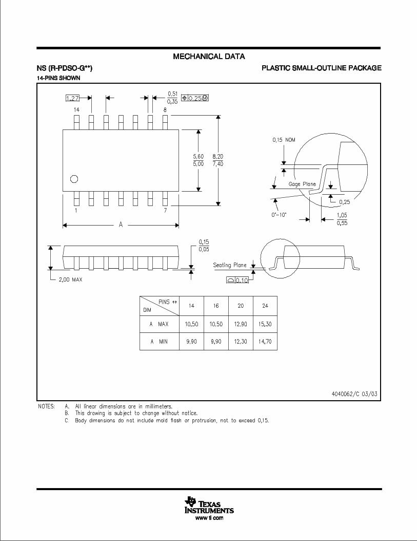
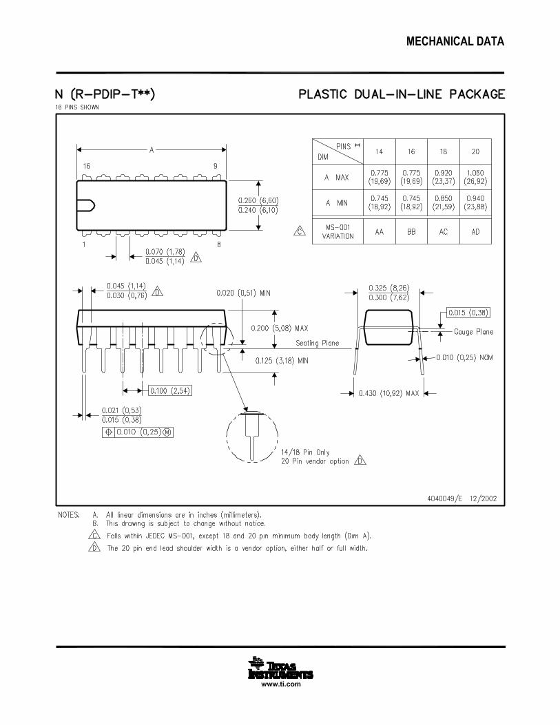
PART NUMBER PACKAGE BODY SIZE (NOM)AM26C31J CDIP (16) 19.56 mm × 6.92 mmAM26C31N PDIP (16) 19.30 mm × 6.35 mmAM26C31NS SO (16) 10.30 mm × 5.30 mmAM26C31W CFP (16) 10.30 mm × 6.73 mmAM26C31D SOIC (16) 9.90 mm × 3.91 mmAM26C31DB SSOP (16) 6.20 mm × 5.30 mmAM26C31PW TSSOP (16) 5.00 mm × 4.40 mmAM26C31FK LCCC (20) 8.89 mm × 8.89 mm
(1) For all available packages, see the orderable addendum atthe end of the data sheet.
Common Application Diagram

2
AM26C31SLLS103O –DECEMBER 1990–REVISED JUNE 2016 www.ti.com
Product Folder Links: AM26C31
Submit Documentation Feedback Copyright © 1990–2016, Texas Instruments Incorporated
Table of Contents1 Features .................................................................. 12 Applications ........................................................... 13 Description ............................................................. 14 Revision History..................................................... 25 Pin Configuration and Functions ......................... 36 Specifications......................................................... 4
6.1 Absolute Maximum Ratings ..................................... 46.2 ESD Ratings.............................................................. 46.3 Recommended Operating Conditions....................... 46.4 Thermal Information .................................................. 56.5 Electrical Characteristics: AM26C31C and
AM26C31I .................................................................. 56.6 Electrical Characteristics: AM26C31Q and
AM26C31M ................................................................ 66.7 Switching Characteristics: AM26C31C and
AM26C31I .................................................................. 66.8 Switching Characteristics: AM26C31Q and
AM26C31M ................................................................ 76.9 Typical Characteristics .............................................. 7
7 Parameter Measurement Information .................. 8
8 Detailed Description ............................................ 108.1 Overview ................................................................. 108.2 Functional Block Diagrams ..................................... 108.3 Feature Description................................................. 118.4 Device Functional Modes........................................ 11
9 Application and Implementation ........................ 129.1 Application Information............................................ 129.2 Typical Application ................................................. 12
10 Power Supply Recommendations ..................... 1311 Layout................................................................... 14
11.1 Layout Guidelines ................................................. 1411.2 Layout Example .................................................... 14
12 Device and Documentation Support ................. 1512.1 Receiving Notification of Documentation Updates 1512.2 Community Resources.......................................... 1512.3 Trademarks ........................................................... 1512.4 Electrostatic Discharge Caution............................ 1512.5 Glossary ................................................................ 15
13 Mechanical, Packaging, and OrderableInformation ........................................................... 15
4 Revision HistoryNOTE: Page numbers for previous revisions may differ from page numbers in the current version.
Changes from Revision N (October 2011) to Revision O Page
• Updated the Features section and added the Applications section, the Device Information table, ESD Ratings table,Feature Description section, Device Functional Modes, Application and Implementation section, Power SupplyRecommendations section, Layout section, Device and Documentation Support section, and Mechanical,Packaging, and Orderable Information section. ..................................................................................................................... 1
• Deleted Ordering Information table, see POA at the end of the data sheet........................................................................... 1• Changed Thermal Information table ....................................................................................................................................... 5
Changes from Revision M (June 2008) to Revision N Page
• Changed units to mA from µA to fix units typo....................................................................................................................... 4
Not to scale
41Z
5G
6NC
72Z
82Y
92
A
10
GN
D
11
NC
12
3A
13
3Y
14 3Z
15 G
16 NC
17 4Z
18 4Y
19
4A
20
VC
C
1N
C
21
A
31
Y
Not to scale
11A 16 VCC
21Y 15 4A
31Z 14 4Y
4G 13 4Z
52Z 12 G
62Y 11 3Z
72A 10 3Y
8GND 9 3A
3
AM26C31www.ti.com SLLS103O –DECEMBER 1990–REVISED JUNE 2016
Product Folder Links: AM26C31
Submit Documentation FeedbackCopyright © 1990–2016, Texas Instruments Incorporated
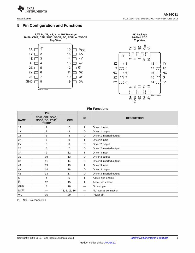
5 Pin Configuration and Functions
J, W, D, DB, NS, N, or PW Package16-Pin CDIP, CFP, SOIC, SSOP, SO, PDIP, or TSSOP
Top View
FK Package20-Pin LCCC
Top View
(1) NC – No connection
Pin FunctionsPIN
I/O DESCRIPTIONNAME
CDIP, CFP, SOIC,SSOP, SO, PDIP,
TSSOPLCCC
1A 1 2 I Driver 1 input1Y 2 3 O Driver 1 output1Z 3 4 O Driver 1 inverted output2A 7 9 I Driver 2 input2Y 6 8 O Driver 2 output2Z 5 7 O Driver 2 inverted output3A 9 12 I Driver 3 input3Y 10 13 O Driver 3 output3Z 11 14 O Driver 3 inverted output4A 15 19 I Driver 3 input4Y 14 18 O Driver 3 output4Z 13 17 O Driver 3 inverted outputG 4 5 I Active high enableG 12 15 I Active low enableGND 8 10 — Ground pinNC (1) — 1, 6, 11, 16 — No internal connectionVCC 16 20 — Power pin

4
AM26C31SLLS103O –DECEMBER 1990–REVISED JUNE 2016 www.ti.com
Product Folder Links: AM26C31
Submit Documentation Feedback Copyright © 1990–2016, Texas Instruments Incorporated
(1) Stresses beyond those listed under Absolute Maximum Ratings may cause permanent damage to the device. These are stress ratingsonly, and functional operation of the device at these or any other conditions beyond those indicated under Recommended OperatingConditions is not implied. Exposure to absolute-maximum-rated conditions for extended periods may affect device reliability.
(2) All voltage values, except differential voltages, are with respect to the network ground terminal.
6 Specifications
6.1 Absolute Maximum Ratingsover operating free-air temperature range (unless otherwise noted) (1)
MIN MAX UNITVCC Supply voltage (2) –0.5 7 VVI Input voltage –0.5 VCC + 0.5 VVID Differential input voltage –14 14 VVO Output voltage –0.5 7IIKIOK
Input or output clamp current ±20 mA
IO Output current ±150 mAVCC current 200 mAGND current –200 mA
TJ Operating virtual junction temperature 150 °CTstg Storage temperature –65 150 °C
(1) JEDEC document JEP155 states that 500-V HBM allows safe manufacturing with a standard ESD control process.(2) JEDEC document JEP157 states that 250-V CDM allows safe manufacturing with a standard ESD control process.
6.2 ESD RatingsVALUE UNIT
V(ESD)Electrostaticdischarge
Human-body model (HBM), per ANSI/ESDA/JEDEC JS-001 (1) ±2000V
Charged-device model (CDM), per JEDEC specification JESD22-C101 (2) ±1000
6.3 Recommended Operating ConditionsMIN NOM MAX UNIT
VCC Supply voltage 4.5 5 5.5 VVID Differential input voltage ±7 VVIH High-level input voltage 2 VVIL Low-level input voltage 0.8 VIOH High-level output current –20 mAIOL Low-level output current 20 mA
TA Operating free-air temperature
AM26C31C 0 70
°CAM26C31I –40 85AM26C31Q –40 125AM26C31M –55 125
5
AM26C31www.ti.com SLLS103O –DECEMBER 1990–REVISED JUNE 2016
Product Folder Links: AM26C31
Submit Documentation FeedbackCopyright © 1990–2016, Texas Instruments Incorporated
(1) For more information about traditional and new thermal metrics, see the Semiconductor and IC Package Thermal Metrics applicationreport.
(2) Maximum power dissipation is a function of TJ(max), RθJA, and TA. The maximum allowable power dissipation at any allowable ambienttemperature is PD = (TJ(max) – TA) / RθJA. Operating at the absolute maximum TJ of 150°C can affect reliability.
(3) The package thermal impedance is calculated in accordance with JESD 51-7.(4) Modelling assumption: MIL-STD-883 for RθJC(top) and RθJC(bot) JESD51 for RθJB.
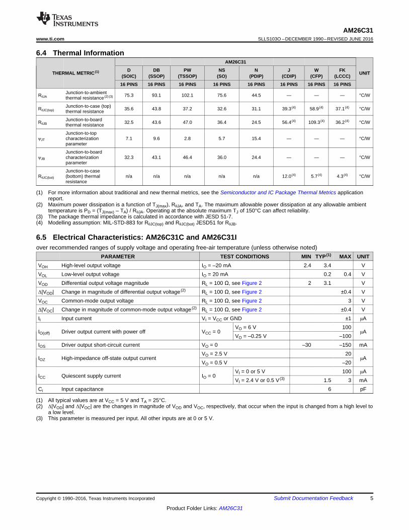
6.4 Thermal Information
THERMAL METRIC (1)
AM26C31
UNITD(SOIC)
DB(SSOP)
PW(TSSOP)
NS(SO)
N(PDIP)
J(CDIP)
W(CFP)
FK(LCCC)
16 PINS 16 PINS 16 PINS 16 PINS 16 PINS 16 PINS 16 PINS 16 PINS
RθJAJunction-to-ambientthermal resistance (2) (3) 75.3 93.1 102.1 75.6 44.5 — — — °C/W
RθJC(top)Junction-to-case (top)thermal resistance 35.6 43.8 37.2 32.6 31.1 39.3 (4) 58.9 (4) 37.1 (4) °C/W
RθJBJunction-to-boardthermal resistance 32.5 43.6 47.0 36.4 24.5 56.4 (4) 109.3 (4) 36.2 (4) °C/W
ψJT
Junction-to-topcharacterizationparameter
7.1 9.6 2.8 5.7 15.4 — — — °C/W
ψJB
Junction-to-boardcharacterizationparameter
32.3 43.1 46.4 36.0 24.4 — — — °C/W
RθJC(bot)
Junction-to-case(bottom) thermalresistance
n/a n/a n/a n/a n/a 12.0 (4) 5.7 (4) 4.3 (4) °C/W
(1) All typical values are at VCC = 5 V and TA = 25°C.(2) Δ|VOD| and Δ|VOC| are the changes in magnitude of VOD and VOC, respectively, that occur when the input is changed from a high level to
a low level.(3) This parameter is measured per input. All other inputs are at 0 or 5 V.
6.5 Electrical Characteristics: AM26C31C and AM26C31Iover recommended ranges of supply voltage and operating free-air temperature (unless otherwise noted)
PARAMETER TEST CONDITIONS MIN TYP (1) MAX UNITVOH High-level output voltage IO = –20 mA 2.4 3.4 VVOL Low-level output voltage IO = 20 mA 0.2 0.4 VVOD Differential output voltage magnitude RL = 100 Ω, see Figure 2 2 3.1 VΔ|VOD| Change in magnitude of differential output voltage (2) RL = 100 Ω, see Figure 2 ±0.4 VVOC Common-mode output voltage RL = 100 Ω, see Figure 2 3 VΔ|VOC| Change in magnitude of common-mode output voltage (2) RL = 100 Ω, see Figure 2 ±0.4 VII Input current VI = VCC or GND ±1 μA
IO(off) Driver output current with power off VCC = 0VO = 6 V 100
μAVO = –0.25 V –100
IOS Driver output short-circuit current VO = 0 –30 –150 mA
IOZ High-impedance off-state output currentVO = 2.5 V 20
μAVO = 0.5 V –20
ICC Quiescent supply current IO = 0VI = 0 or 5 V 100 μAVI = 2.4 V or 0.5 V (3) 1.5 3 mA
Ci Input capacitance 6 pF

6
AM26C31SLLS103O –DECEMBER 1990–REVISED JUNE 2016 www.ti.com
Product Folder Links: AM26C31
Submit Documentation Feedback Copyright © 1990–2016, Texas Instruments Incorporated
(1) All typical values are at VCC = 5 V and TA = 25°C.(2) Δ|VOD| and Δ|VOC| are the changes in magnitude of VOD and VOC, respectively, that occur when the input is changed from a high level to
a low level.(3) This parameter is measured per input. All other inputs are at 0 or 5 V.
6.6 Electrical Characteristics: AM26C31Q and AM26C31Mover recommended ranges of supply voltage and operating free-air temperature (unless otherwise noted)
PARAMETER TEST CONDITIONS MIN TYP (1) MAX UNITVOH High-level output voltage IO = –20 mA 2.2 3.4 VVOL Low-level output voltage IO = 20 mA 0.2 0.4 VVOD Differential output voltage magnitude RL = 100 Ω, see Figure 2 2 3.1 VΔ|VOD| Change in magnitude of differential output voltage (2) RL = 100 Ω, see Figure 2 ±0.4 VVOC Common-mode output voltage RL = 100 Ω, see Figure 2 3 VΔ|VOC| Change in magnitude of common-mode output voltage (2) RL = 100 Ω, see Figure 2 ±0.4 VII Input current VI = VCC or GND ±1 μA
IO(off) Driver output current with power off VCC = 0VO = 6 V 100
μAVO = –0.25 V –100
IOS Driver output short-circuit current VO = 0 –170 mA
IOZ High-impedance off-state output currentVO = 2.5 V 20
μAVO = 0.5 V –20
ICC Quiescent supply current IO = 0VI = 0 or 5 V 100 μAVI = 2.4 V or 0.5 V (3) 3.2 mA
Ci Input capacitance 6 pF
(1) All typical values are at VCC = 5 V and TA = 25°C.(2) Cpd is used to estimate the switching losses according to PD = Cpd × VCC
2 × f, where f is the switching frequency.
6.7 Switching Characteristics: AM26C31C and AM26C31Iover recommended ranges of supply voltage and operating free-air temperature (unless otherwise noted)
PARAMETER TEST CONDITIONS MIN TYP (1) MAX UNITtPLH Propagation delay time, low-to-high-level output
S1 is open, see Figure 33 7 12
nstPHL Propagation delay time, high-to-low-level output 3 7 12tsk(p) Pulse skew time (|tPLH – tPHL|) S1 is open, see Figure 3 0.5 4 nstr(OD), tf(OD) Differential output rise and fall times S1 is open, see Figure 4 5 10 nstPZH Output enable time to high level
S1 is closed, see Figure 510 19
nstPZL Output enable time to low level 10 19tPHZ Output disable time from high level
S1 is closed, see Figure 57 16
nstPLZ Output disable time from low level 7 16Cpd Power dissipation capacitance (each driver) (2) S1 is open, see Figure 3 170 pF

7
AM26C31www.ti.com SLLS103O –DECEMBER 1990–REVISED JUNE 2016
Product Folder Links: AM26C31
Submit Documentation FeedbackCopyright © 1990–2016, Texas Instruments Incorporated
(1) All typical values are at VCC = 5 V and TA = 25°C.(2) Cpd is used to estimate the switching losses according to PD = Cpd × VCC
2 × f, where f is the switching frequency.
6.8 Switching Characteristics: AM26C31Q and AM26C31Mover recommended ranges of supply voltage and operating free-air temperature (unless otherwise noted)
PARAMETER TEST CONDITIONS MIN TYP (1) MAX UNIT
tPLHPropagation delay time, low-to-high-leveloutput
S1 is open, see Figure 37 12
nstPHL
Propagation delay time, high-to-low-leveloutput 6.5 12
tsk(p) Pulse skew time (|tPLH – tPHL|) S1 is open, see Figure 3 0.5 4 nstr(OD), tf(OD) Differential output rise and fall times S1 is open, see Figure 4 5 12 nstPZH Output enable time to high level
S1 is closed, see Figure 510 19
nstPZL Output enable time to low level 10 19tPHZ Output disable time from high level
S1 is closed, see Figure 57 16
nstPLZ Output disable time from low level 7 16
CpdPower dissipation capacitance (eachdriver) (2) S1 is open, see Figure 3 100 pF
6.9 Typical Characteristics
Figure 1. Supply Current vs Switching Frequency
Input A
(see Note B)
Output Y
1.3 V
50%
tsk(p)
Output Z
tPHL tPLH
tsk(p)
tPLH tPHL
C3 = 40 pF
C2 = 40 pF
C1 =
40 pFInput
See Note A
TEST CIRCUIT
RL/2
RL/2
1.5 V500 Ω
S1
1.3 V
1.3 V
3 V
0 V
50%
50%
50%
8
AM26C31SLLS103O –DECEMBER 1990–REVISED JUNE 2016 www.ti.com
Product Folder Links: AM26C31
Submit Documentation Feedback Copyright © 1990–2016, Texas Instruments Incorporated
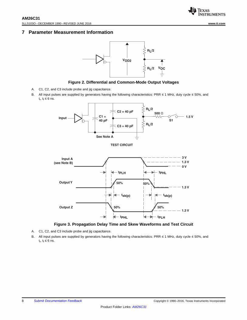
7 Parameter Measurement Information
Figure 2. Differential and Common-Mode Output VoltagesA. C1, C2, and C3 include probe and jig capacitance.B. All input pulses are supplied by generators having the following characteristics: PRR ≤ 1 MHz, duty cycle ≤ 50%, and
tr, tf ≤ 6 ns.
Figure 3. Propagation Delay Time and Skew Waveforms and Test CircuitA. C1, C2, and C3 include probe and jig capacitance.B. All input pulses are supplied by generators having the following characteristics: PRR ≤ 1 MHz, duty cycle ≤ 50%, and
tr, tf ≤ 6 ns.

Enable G Input
(see Note C)
Output WIth
0 V to A InputVOL + 0.3 V
tPLZ
tPHZ tPZH
tPZL
C3 =
40 pF
C2 =
40 pF
C1 =
40 pFInput A
50 Ω
50 Ω
500 Ω
TEST CIRCUIT
VOLTAGE WAVEFORMS
3 V
0 V
1.5 V
VOL
VOHVOH - 0.3 V
1.5 V
See Note A
G
G
Enable G Input
Output
Output
Output WIth
3 V to A Input
Enable Inputs
(see Note B)
0 V
3 V1.5 V
S1
1.3 V1.3 V
2 V
0.8 V
9
AM26C31www.ti.com SLLS103O –DECEMBER 1990–REVISED JUNE 2016
Product Folder Links: AM26C31
Submit Documentation FeedbackCopyright © 1990–2016, Texas Instruments Incorporated
Parameter Measurement Information (continued)
Figure 4. Differential-Output Rise- and Fall-Time Waveforms and Test CircuitA. C1, C2, and C3 include probe and jig capacitance.B. All input pulses are supplied by generators having the following characteristics: PRR ≤ 1 MHz, duty cycle ≤ 50%, and
tr, tf ≤ 6 ns.C. Each enable is tested separately.
Figure 5. Output Enable and Disable Time Waveforms and Test Circuit

1A
G
2A
4A
G
3A
1
4
7
9
12
15
3Y10
3Z11
1Y2
1Z3
4Y14
4Z13
2Y6
2Z5
Copyright © 2016, Texas Instruments Incorporated
10
AM26C31SLLS103O –DECEMBER 1990–REVISED JUNE 2016 www.ti.com
Product Folder Links: AM26C31
Submit Documentation Feedback Copyright © 1990–2016, Texas Instruments Incorporated
8 Detailed Description
8.1 OverviewThe AM26C31 is a quadruple differential line driver with complementary outputs. The device is designed to meetthe requirements of TIA/EIA-422-B and ITU (formerly CCITT), and it is generally used to communicate overrelatively long wires in noisy environments.
8.2 Functional Block Diagrams
Pin numbers shown are for the D, DB, J, N, NS, PW, and W packages.
Figure 6. Logic Diagram (Positive Logic)

Input
VCC
TYPICAL OF ALL OUTPUTS
Output
VCC
GND GND
EQUIVALENT OF EACH INPUT
Copyright © 2016, Texas Instruments Incorporated
11
AM26C31www.ti.com SLLS103O –DECEMBER 1990–REVISED JUNE 2016
Product Folder Links: AM26C31
Submit Documentation FeedbackCopyright © 1990–2016, Texas Instruments Incorporated
Functional Block Diagrams (continued)
Figure 7. Schematics of Inputs and Outputs
8.3 Feature Description
8.3.1 Active-High and Active-LowThe device can be configured using the G and G logic inputs to select transmitter output. A logic high on the Gpin or a logic low on the G pin enables the device to operate. These pins are simply a way to configure the logicto match that of the receiving or transmitting controller or microprocessor.
8.3.2 Operates from a Single 5-V SupplyBoth the logic and transmitters operate from a single 5-V rail, making designs much more simple. The line driversand receivers can operate off the same rail as the host controller or a similar low voltage supply, thus simplifyingpower structure.
8.4 Device Functional ModesTable 1 lists the functional modes of the AM26C31.
(1) H = High level,L = Low level,X = Irrelevant,Z = High impedance (off)
Table 1. Function Table (Each Driver) (1)
INPUTA
ENABLES OUTPUTSG G Y Z
H H X H LL H X L HH X L H LL X L L HX L H Z Z

1
2
3
4
5
6
7
8
16
15
14
13
12
11
10
9
1A
1Y
1Z
G
2Z
2Y
2A
GND
VCC
4A
4Y
4Z
G
3Z
3Y
3A
VCC
Input 1 Signal
Output 1Differential Pair
Input 2 Signal
Output 2Differential Pair
Output 4Differential Pair
Input 4 Signal
Output 3Differential Pair
Input 3 Signal
Active Low Enable Signal
0.1 PF
Copyright © 2016, Texas Instruments Incorporated
12
AM26C31SLLS103O –DECEMBER 1990–REVISED JUNE 2016 www.ti.com
Product Folder Links: AM26C31
Submit Documentation Feedback Copyright © 1990–2016, Texas Instruments Incorporated
9 Application and Implementation
NOTEInformation in the following applications sections is not part of the TI componentspecification, and TI does not warrant its accuracy or completeness. TI’s customers areresponsible for determining suitability of components for their purposes. Customers shouldvalidate and test their design implementation to confirm system functionality.
9.1 Application InformationWhen designing a system that uses drivers, receivers, and transceivers that comply with RS-422, proper cabletermination is essential for highly reliable applications with reduced reflections in the transmission line. BecauseRS-422 allows only one driver on the bus, if termination is used, it is placed only at the end of the cable near thelast receiver. Factors to consider when determining the type of termination usually are performance requirementsof the application and the ever-present factor, cost. The different types of termination techniques discussed areunterminated lines, parallel termination, AC termination, and multipoint termination. For laboratory experiments,100 feet of 100-Ω, 24-AWG, twisted-pair cable (Bertek) was used. A single driver and receiver, TI AM26C31Cand AM26C32C, respectively, were tested at room temperature with a 5-V supply voltage. To show voltagewaveforms related to transmission-line reflections, the first plot shows output waveforms from the driver at thestart of the cable (A/B); the second plot shows input waveforms to the receiver at the far end of the cable (Y).
9.2 Typical Application
Figure 8. Differential Terminated Configuration With All Channels and Active Low Enable Used
9.2.1 Design RequirementsResistor and capacitor (if used) termination values are shown for each laboratory experiment, but vary fromsystem to system. For example, the termination resistor, RT, must be within 20% of the characteristic impedance,Zo, of the cable and can vary from about 80 Ω to 120 Ω.

±3
±2
±1
0
1
2
3
4
5
0 0.1 0.2 0.3 0.4 0.5
Vol
tage
(V
)
Time (s)
Y A/B
C001
13
AM26C31www.ti.com SLLS103O –DECEMBER 1990–REVISED JUNE 2016
Product Folder Links: AM26C31
Submit Documentation FeedbackCopyright © 1990–2016, Texas Instruments Incorporated
Typical Application (continued)9.2.2 Detailed Design ProcedureEnsure values in Absolute Maximum Ratings are not exceeded.
Supply voltage, VIH, and VIL must comply with Recommended Operating Conditions.
9.2.3 Application Curve
Figure 9. Differential 120-Ω Terminated Output Waveforms (Cat 5E Cable)
10 Power Supply RecommendationsPlace 0.1-µF bypass capacitors close to the power-supply pins to reduce errors coupling in from noisy or highimpedance power supplies.

Input 2
1A1
2
3
4
5
6
7
8
16
15
14
13
12
11
10
9
VCC
0.1 PF
AM26C31
1Y
1Z
Differential Output 1
Input 1
2Y
2A
GND
G
2Z
VCC
4A
4Y
3Z
3Y
3A
4Z
GDifferential Output 2
Active Low Enable
14
AM26C31SLLS103O –DECEMBER 1990–REVISED JUNE 2016 www.ti.com
Product Folder Links: AM26C31
Submit Documentation Feedback Copyright © 1990–2016, Texas Instruments Incorporated
11 Layout
11.1 Layout GuidelinesFor best operational performance of the device, use good PCB layout practices, including:• Noise can propagate into analog circuitry through the power pins of the circuit as a whole, as well as the
operational amplifier. Bypass capacitors are used to reduce the coupled noise by providing low impedancepower sources local to the analog circuitry.– Connect low-ESR, 0.1-µF ceramic bypass capacitors between each supply pin and ground, placed as
close to the device as possible. A single bypass capacitor from V+ to ground is applicable for single-supply applications.
• Separate grounding for analog and digital portions of circuitry is one of the simplest and most effectivemethods of noise suppression. One or more layers on multilayer PCBs are usually devoted to ground planes.A ground plane helps distribute heat and reduces EMI noise pickup. Make sure to physically separate digitaland analog grounds, paying attention to the flow of the ground current.
• To reduce parasitic coupling, run the input traces as far away from the supply or output traces as possible. Ifit is not possible to keep them separate, it is much better to cross the sensitive trace perpendicular asopposed to in parallel with the noisy trace.
• Place the external components as close to the device as possible. Keeping RF and RG close to the invertinginput minimizes parasitic capacitance.
• Keep the length of input traces as short as possible. Always remember that the input traces are the mostsensitive part of the circuit.
• Consider a driven, low-impedance guard ring around the critical traces. A guard ring can significantly reduceleakage currents from nearby traces that are at different potentials.
11.2 Layout Example
Figure 10. Trace Layout on PCB and Recommendations

15
AM26C31www.ti.com SLLS103O –DECEMBER 1990–REVISED JUNE 2016
Product Folder Links: AM26C31
Submit Documentation FeedbackCopyright © 1990–2016, Texas Instruments Incorporated
12 Device and Documentation Support
12.1 Receiving Notification of Documentation UpdatesTo receive notification of documentation updates, navigate to the device product folder on ti.com. In the upperright corner, click on Alert me to register and receive a weekly digest of any product information that haschanged. For change details, review the revision history included in any revised document.
12.2 Community ResourcesThe following links connect to TI community resources. Linked contents are provided "AS IS" by the respectivecontributors. They do not constitute TI specifications and do not necessarily reflect TI's views; see TI's Terms ofUse.
TI E2E™ Online Community TI's Engineer-to-Engineer (E2E) Community. Created to foster collaborationamong engineers. At e2e.ti.com, you can ask questions, share knowledge, explore ideas and helpsolve problems with fellow engineers.
Design Support TI's Design Support Quickly find helpful E2E forums along with design support tools andcontact information for technical support.
12.3 TrademarksE2E is a trademark of Texas Instruments.All other trademarks are the property of their respective owners.
12.4 Electrostatic Discharge CautionThese devices have limited built-in ESD protection. The leads should be shorted together or the device placed in conductive foamduring storage or handling to prevent electrostatic damage to the MOS gates.
12.5 GlossarySLYZ022 — TI Glossary.
This glossary lists and explains terms, acronyms, and definitions.
13 Mechanical, Packaging, and Orderable InformationThe following pages include mechanical packaging and orderable information. This information is the mostcurrent data available for the designated devices. This data is subject to change without notice and revision ofthis document. For browser based versions of this data sheet, refer to the left hand navigation.

PACKAGE OPTION ADDENDUM
www.ti.com 17-Mar-2017
Addendum-Page 1
PACKAGING INFORMATION
Orderable Device Status(1)
Package Type PackageDrawing
Pins PackageQty
Eco Plan(2)
Lead/Ball Finish(6)
MSL Peak Temp(3)
Op Temp (°C) Device Marking(4/5)
Samples
5962-9163901M2A ACTIVE LCCC FK 20 1 TBD POST-PLATE N / A for Pkg Type -55 to 125 5962-9163901M2AAM26C31M
5962-9163901MEA ACTIVE CDIP J 16 1 TBD A42 N / A for Pkg Type -55 to 125 5962-9163901MEAAM26C31M
5962-9163901MFA ACTIVE CFP W 16 1 TBD A42 N / A for Pkg Type -55 to 125 5962-9163901MFAAM26C31M
5962-9163901Q2A ACTIVE LCCC FK 20 1 TBD POST-PLATE N / A for Pkg Type -55 to 125 5962-9163901Q2AAM26C31MFKB
5962-9163901QEA ACTIVE CDIP J 16 1 TBD A42 N / A for Pkg Type -55 to 125 5962-9163901QEAAM26C31MJB
5962-9163901QFA ACTIVE CFP W 16 1 TBD A42 N / A for Pkg Type -55 to 125 5962-9163901QFAAM26C31MWB
AM26C31CD ACTIVE SOIC D 16 40 Green (RoHS& no Sb/Br)
CU NIPDAU Level-1-260C-UNLIM 0 to 70 AM26C31C
AM26C31CDBR ACTIVE SSOP DB 16 2000 Green (RoHS& no Sb/Br)
CU NIPDAU Level-1-260C-UNLIM 0 to 70 26C31
AM26C31CDBRG4 ACTIVE SSOP DB 16 2000 Green (RoHS& no Sb/Br)
CU NIPDAU Level-1-260C-UNLIM 0 to 70 26C31
AM26C31CDE4 ACTIVE SOIC D 16 40 Green (RoHS& no Sb/Br)
CU NIPDAU Level-1-260C-UNLIM 0 to 70 AM26C31C
AM26C31CDG4 ACTIVE SOIC D 16 40 Green (RoHS& no Sb/Br)
CU NIPDAU Level-1-260C-UNLIM 0 to 70 AM26C31C
AM26C31CDR ACTIVE SOIC D 16 2500 Green (RoHS& no Sb/Br)
CU NIPDAU Level-1-260C-UNLIM 0 to 70 AM26C31C
AM26C31CDRE4 ACTIVE SOIC D 16 2500 Green (RoHS& no Sb/Br)
CU NIPDAU Level-1-260C-UNLIM 0 to 70 AM26C31C
AM26C31CDRG4 ACTIVE SOIC D 16 2500 Green (RoHS& no Sb/Br)
CU NIPDAU Level-1-260C-UNLIM 0 to 70 AM26C31C

PACKAGE OPTION ADDENDUM
www.ti.com 17-Mar-2017
Addendum-Page 2
Orderable Device Status(1)
Package Type PackageDrawing
Pins PackageQty
Eco Plan(2)
Lead/Ball Finish(6)
MSL Peak Temp(3)
Op Temp (°C) Device Marking(4/5)
Samples
AM26C31CN ACTIVE PDIP N 16 25 Pb-Free(RoHS)
CU NIPDAU N / A for Pkg Type 0 to 70 AM26C31CN
AM26C31CNE4 ACTIVE PDIP N 16 25 Pb-Free(RoHS)
CU NIPDAU N / A for Pkg Type 0 to 70 AM26C31CN
AM26C31CNSR ACTIVE SO NS 16 2000 Green (RoHS& no Sb/Br)
CU NIPDAU Level-1-260C-UNLIM 0 to 70 26C31
AM26C31CNSRG4 ACTIVE SO NS 16 2000 Green (RoHS& no Sb/Br)
CU NIPDAU Level-1-260C-UNLIM 0 to 70 26C31
AM26C31ID ACTIVE SOIC D 16 40 Green (RoHS& no Sb/Br)
CU NIPDAU Level-1-260C-UNLIM -40 to 85 AM26C31I
AM26C31IDBR ACTIVE SSOP DB 16 2000 Green (RoHS& no Sb/Br)
CU NIPDAU Level-1-260C-UNLIM -40 to 85 26C31I
AM26C31IDBRE4 ACTIVE SSOP DB 16 2000 Green (RoHS& no Sb/Br)
CU NIPDAU Level-1-260C-UNLIM -40 to 85 26C31I
AM26C31IDBRG4 ACTIVE SSOP DB 16 2000 Green (RoHS& no Sb/Br)
CU NIPDAU Level-1-260C-UNLIM -40 to 85 26C31I
AM26C31IDE4 ACTIVE SOIC D 16 40 Green (RoHS& no Sb/Br)
CU NIPDAU Level-1-260C-UNLIM -40 to 85 AM26C31I
AM26C31IDG4 ACTIVE SOIC D 16 40 Green (RoHS& no Sb/Br)
CU NIPDAU Level-1-260C-UNLIM -40 to 85 AM26C31I
AM26C31IDR ACTIVE SOIC D 16 2500 Green (RoHS& no Sb/Br)
CU NIPDAU | CU SN Level-1-260C-UNLIM -40 to 85 AM26C31I
AM26C31IDRE4 ACTIVE SOIC D 16 2500 Green (RoHS& no Sb/Br)
CU NIPDAU Level-1-260C-UNLIM -40 to 85 AM26C31I
AM26C31IDRG4 ACTIVE SOIC D 16 2500 Green (RoHS& no Sb/Br)
CU NIPDAU Level-1-260C-UNLIM -40 to 85 AM26C31I
AM26C31IN ACTIVE PDIP N 16 25 Pb-Free(RoHS)
CU NIPDAU N / A for Pkg Type -40 to 85 AM26C31IN
AM26C31INE4 ACTIVE PDIP N 16 25 Pb-Free(RoHS)
CU NIPDAU N / A for Pkg Type -40 to 85 AM26C31IN
AM26C31INSR ACTIVE SO NS 16 2000 Green (RoHS& no Sb/Br)
CU NIPDAU Level-1-260C-UNLIM -40 to 85 26C31I
AM26C31IPW ACTIVE TSSOP PW 16 90 Green (RoHS& no Sb/Br)
CU NIPDAU Level-1-260C-UNLIM -40 to 85 26C31I
AM26C31IPWG4 ACTIVE TSSOP PW 16 90 Green (RoHS& no Sb/Br)
CU NIPDAU Level-1-260C-UNLIM -40 to 85 26C31I

PACKAGE OPTION ADDENDUM
www.ti.com 17-Mar-2017
Addendum-Page 3
Orderable Device Status(1)
Package Type PackageDrawing
Pins PackageQty
Eco Plan(2)
Lead/Ball Finish(6)
MSL Peak Temp(3)
Op Temp (°C) Device Marking(4/5)
Samples
AM26C31IPWR ACTIVE TSSOP PW 16 2000 Green (RoHS& no Sb/Br)
CU NIPDAU | CU SN Level-1-260C-UNLIM -40 to 85 26C31I
AM26C31IPWRG4 ACTIVE TSSOP PW 16 2000 Green (RoHS& no Sb/Br)
CU NIPDAU Level-1-260C-UNLIM -40 to 85 26C31I
AM26C31MFKB ACTIVE LCCC FK 20 1 TBD POST-PLATE N / A for Pkg Type -55 to 125 5962-9163901Q2AAM26C31MFKB
AM26C31MJB ACTIVE CDIP J 16 1 TBD A42 N / A for Pkg Type -55 to 125 5962-9163901QEAAM26C31MJB
AM26C31MWB ACTIVE CFP W 16 1 TBD A42 N / A for Pkg Type -55 to 125 5962-9163901QFAAM26C31MWB
AM26C31QD ACTIVE SOIC D 16 40 Green (RoHS& no Sb/Br)
CU NIPDAU Level-1-260C-UNLIM -40 to 125 AM26C31Q
AM26C31QDG4 ACTIVE SOIC D 16 40 Green (RoHS& no Sb/Br)
CU NIPDAU Level-1-260C-UNLIM -40 to 125 26C31Q
AM26C31QDR ACTIVE SOIC D 16 2500 Green (RoHS& no Sb/Br)
CU NIPDAU Level-1-260C-UNLIM -40 to 125 AM26C31Q
AM26C31QDRG4 ACTIVE SOIC D 16 2500 Green (RoHS& no Sb/Br)
CU NIPDAU Level-1-260C-UNLIM -40 to 125 26C31Q
(1) The marketing status values are defined as follows:ACTIVE: Product device recommended for new designs.LIFEBUY: TI has announced that the device will be discontinued, and a lifetime-buy period is in effect.NRND: Not recommended for new designs. Device is in production to support existing customers, but TI does not recommend using this part in a new design.PREVIEW: Device has been announced but is not in production. Samples may or may not be available.OBSOLETE: TI has discontinued the production of the device.
(2) Eco Plan - The planned eco-friendly classification: Pb-Free (RoHS), Pb-Free (RoHS Exempt), or Green (RoHS & no Sb/Br) - please check http://www.ti.com/productcontent for the latest availabilityinformation and additional product content details.TBD: The Pb-Free/Green conversion plan has not been defined.Pb-Free (RoHS): TI's terms "Lead-Free" or "Pb-Free" mean semiconductor products that are compatible with the current RoHS requirements for all 6 substances, including the requirement thatlead not exceed 0.1% by weight in homogeneous materials. Where designed to be soldered at high temperatures, TI Pb-Free products are suitable for use in specified lead-free processes.Pb-Free (RoHS Exempt): This component has a RoHS exemption for either 1) lead-based flip-chip solder bumps used between the die and package, or 2) lead-based die adhesive used betweenthe die and leadframe. The component is otherwise considered Pb-Free (RoHS compatible) as defined above.Green (RoHS & no Sb/Br): TI defines "Green" to mean Pb-Free (RoHS compatible), and free of Bromine (Br) and Antimony (Sb) based flame retardants (Br or Sb do not exceed 0.1% by weightin homogeneous material)
PACKAGE OPTION ADDENDUM
www.ti.com 17-Mar-2017
Addendum-Page 4
(3) MSL, Peak Temp. - The Moisture Sensitivity Level rating according to the JEDEC industry standard classifications, and peak solder temperature.
(4) There may be additional marking, which relates to the logo, the lot trace code information, or the environmental category on the device.
(5) Multiple Device Markings will be inside parentheses. Only one Device Marking contained in parentheses and separated by a "~" will appear on a device. If a line is indented then it is a continuationof the previous line and the two combined represent the entire Device Marking for that device.
(6) Lead/Ball Finish - Orderable Devices may have multiple material finish options. Finish options are separated by a vertical ruled line. Lead/Ball Finish values may wrap to two lines if the finishvalue exceeds the maximum column width.
Important Information and Disclaimer:The information provided on this page represents TI's knowledge and belief as of the date that it is provided. TI bases its knowledge and belief on informationprovided by third parties, and makes no representation or warranty as to the accuracy of such information. Efforts are underway to better integrate information from third parties. TI has taken andcontinues to take reasonable steps to provide representative and accurate information but may not have conducted destructive testing or chemical analysis on incoming materials and chemicals.TI and TI suppliers consider certain information to be proprietary, and thus CAS numbers and other limited information may not be available for release.
In no event shall TI's liability arising out of such information exceed the total purchase price of the TI part(s) at issue in this document sold by TI to Customer on an annual basis.
OTHER QUALIFIED VERSIONS OF AM26C31, AM26C31M :
• Catalog: AM26C31
• Enhanced Product: AM26C31-EP, AM26C31-EP
• Military: AM26C31M
NOTE: Qualified Version Definitions:
• Catalog - TI's standard catalog product
• Enhanced Product - Supports Defense, Aerospace and Medical Applications
• Military - QML certified for Military and Defense Applications

TAPE AND REEL INFORMATION
*All dimensions are nominal
Device PackageType
PackageDrawing
Pins SPQ ReelDiameter
(mm)
ReelWidth
W1 (mm)
A0(mm)
B0(mm)
K0(mm)
P1(mm)
W(mm)
Pin1Quadrant
AM26C31CDBR SSOP DB 16 2000 330.0 16.4 8.2 6.6 2.5 12.0 16.0 Q1
AM26C31CDR SOIC D 16 2500 330.0 16.4 6.5 10.3 2.1 8.0 16.0 Q1
AM26C31IDBR SSOP DB 16 2000 330.0 16.4 8.2 6.6 2.5 12.0 16.0 Q1
AM26C31IDR SOIC D 16 2500 330.0 16.4 6.5 10.3 2.1 8.0 16.0 Q1
AM26C31IDR SOIC D 16 2500 330.0 16.8 6.5 10.3 2.1 8.0 16.0 Q1
AM26C31IDRG4 SOIC D 16 2500 330.0 16.4 6.5 10.3 2.1 8.0 16.0 Q1
AM26C31IPWR TSSOP PW 16 2000 330.0 12.4 6.9 5.6 1.6 8.0 12.0 Q1
AM26C31IPWR TSSOP PW 16 2000 330.0 12.4 6.9 5.6 1.6 8.0 12.0 Q1
AM26C31IPWRG4 TSSOP PW 16 2000 330.0 12.4 6.9 5.6 1.6 8.0 12.0 Q1
AM26C31QDR SOIC D 16 2500 330.0 16.4 6.5 10.3 2.1 8.0 16.0 Q1
AM26C31QDRG4 SOIC D 16 2500 330.0 16.4 6.5 10.3 2.1 8.0 16.0 Q1
PACKAGE MATERIALS INFORMATION
www.ti.com 14-Mar-2016
Pack Materials-Page 1

*All dimensions are nominal
Device Package Type Package Drawing Pins SPQ Length (mm) Width (mm) Height (mm)
AM26C31CDBR SSOP DB 16 2000 367.0 367.0 38.0
AM26C31CDR SOIC D 16 2500 333.2 345.9 28.6
AM26C31IDBR SSOP DB 16 2000 367.0 367.0 38.0
AM26C31IDR SOIC D 16 2500 333.2 345.9 28.6
AM26C31IDR SOIC D 16 2500 364.0 364.0 27.0
AM26C31IDRG4 SOIC D 16 2500 333.2 345.9 28.6
AM26C31IPWR TSSOP PW 16 2000 364.0 364.0 27.0
AM26C31IPWR TSSOP PW 16 2000 367.0 367.0 35.0
AM26C31IPWRG4 TSSOP PW 16 2000 367.0 367.0 35.0
AM26C31QDR SOIC D 16 2500 367.0 367.0 38.0
AM26C31QDRG4 SOIC D 16 2500 333.2 345.9 28.6
PACKAGE MATERIALS INFORMATION
www.ti.com 14-Mar-2016
Pack Materials-Page 2


MECHANICAL DATA
MSSO002E – JANUARY 1995 – REVISED DECEMBER 2001
POST OFFICE BOX 655303 • DALLAS, TEXAS 75265
DB (R-PDSO-G**) PLASTIC SMALL-OUTLINE
4040065 /E 12/01
28 PINS SHOWN
Gage Plane
8,207,40
0,550,95
0,25
38
12,90
12,30
28
10,50
24
8,50
Seating Plane
9,907,90
30
10,50
9,90
0,38
5,605,00
15
0,22
14
A
28
1
2016
6,506,50
14
0,05 MIN
5,905,90
DIM
A MAX
A MIN
PINS **
2,00 MAX
6,90
7,50
0,65 M0,15
0°–8°
0,10
0,090,25
NOTES: A. All linear dimensions are in millimeters.B. This drawing is subject to change without notice.C. Body dimensions do not include mold flash or protrusion not to exceed 0,15.D. Falls within JEDEC MO-150

IMPORTANT NOTICE
Texas Instruments Incorporated (TI) reserves the right to make corrections, enhancements, improvements and other changes to itssemiconductor products and services per JESD46, latest issue, and to discontinue any product or service per JESD48, latest issue. Buyersshould obtain the latest relevant information before placing orders and should verify that such information is current and complete.TI’s published terms of sale for semiconductor products (http://www.ti.com/sc/docs/stdterms.htm) apply to the sale of packaged integratedcircuit products that TI has qualified and released to market. Additional terms may apply to the use or sale of other types of TI products andservices.Reproduction of significant portions of TI information in TI data sheets is permissible only if reproduction is without alteration and isaccompanied by all associated warranties, conditions, limitations, and notices. TI is not responsible or liable for such reproduceddocumentation. Information of third parties may be subject to additional restrictions. Resale of TI products or services with statementsdifferent from or beyond the parameters stated by TI for that product or service voids all express and any implied warranties for theassociated TI product or service and is an unfair and deceptive business practice. TI is not responsible or liable for any such statements.Buyers and others who are developing systems that incorporate TI products (collectively, “Designers”) understand and agree that Designersremain responsible for using their independent analysis, evaluation and judgment in designing their applications and that Designers havefull and exclusive responsibility to assure the safety of Designers' applications and compliance of their applications (and of all TI productsused in or for Designers’ applications) with all applicable regulations, laws and other applicable requirements. Designer represents that, withrespect to their applications, Designer has all the necessary expertise to create and implement safeguards that (1) anticipate dangerousconsequences of failures, (2) monitor failures and their consequences, and (3) lessen the likelihood of failures that might cause harm andtake appropriate actions. Designer agrees that prior to using or distributing any applications that include TI products, Designer willthoroughly test such applications and the functionality of such TI products as used in such applications.TI’s provision of technical, application or other design advice, quality characterization, reliability data or other services or information,including, but not limited to, reference designs and materials relating to evaluation modules, (collectively, “TI Resources”) are intended toassist designers who are developing applications that incorporate TI products; by downloading, accessing or using TI Resources in anyway, Designer (individually or, if Designer is acting on behalf of a company, Designer’s company) agrees to use any particular TI Resourcesolely for this purpose and subject to the terms of this Notice.TI’s provision of TI Resources does not expand or otherwise alter TI’s applicable published warranties or warranty disclaimers for TIproducts, and no additional obligations or liabilities arise from TI providing such TI Resources. TI reserves the right to make corrections,enhancements, improvements and other changes to its TI Resources. TI has not conducted any testing other than that specificallydescribed in the published documentation for a particular TI Resource.Designer is authorized to use, copy and modify any individual TI Resource only in connection with the development of applications thatinclude the TI product(s) identified in such TI Resource. NO OTHER LICENSE, EXPRESS OR IMPLIED, BY ESTOPPEL OR OTHERWISETO ANY OTHER TI INTELLECTUAL PROPERTY RIGHT, AND NO LICENSE TO ANY TECHNOLOGY OR INTELLECTUAL PROPERTYRIGHT OF TI OR ANY THIRD PARTY IS GRANTED HEREIN, including but not limited to any patent right, copyright, mask work right, orother intellectual property right relating to any combination, machine, or process in which TI products or services are used. Informationregarding or referencing third-party products or services does not constitute a license to use such products or services, or a warranty orendorsement thereof. Use of TI Resources may require a license from a third party under the patents or other intellectual property of thethird party, or a license from TI under the patents or other intellectual property of TI.TI RESOURCES ARE PROVIDED “AS IS” AND WITH ALL FAULTS. TI DISCLAIMS ALL OTHER WARRANTIES ORREPRESENTATIONS, EXPRESS OR IMPLIED, REGARDING RESOURCES OR USE THEREOF, INCLUDING BUT NOT LIMITED TOACCURACY OR COMPLETENESS, TITLE, ANY EPIDEMIC FAILURE WARRANTY AND ANY IMPLIED WARRANTIES OFMERCHANTABILITY, FITNESS FOR A PARTICULAR PURPOSE, AND NON-INFRINGEMENT OF ANY THIRD PARTY INTELLECTUALPROPERTY RIGHTS. TI SHALL NOT BE LIABLE FOR AND SHALL NOT DEFEND OR INDEMNIFY DESIGNER AGAINST ANY CLAIM,INCLUDING BUT NOT LIMITED TO ANY INFRINGEMENT CLAIM THAT RELATES TO OR IS BASED ON ANY COMBINATION OFPRODUCTS EVEN IF DESCRIBED IN TI RESOURCES OR OTHERWISE. IN NO EVENT SHALL TI BE LIABLE FOR ANY ACTUAL,DIRECT, SPECIAL, COLLATERAL, INDIRECT, PUNITIVE, INCIDENTAL, CONSEQUENTIAL OR EXEMPLARY DAMAGES INCONNECTION WITH OR ARISING OUT OF TI RESOURCES OR USE THEREOF, AND REGARDLESS OF WHETHER TI HAS BEENADVISED OF THE POSSIBILITY OF SUCH DAMAGES.Unless TI has explicitly designated an individual product as meeting the requirements of a particular industry standard (e.g., ISO/TS 16949and ISO 26262), TI is not responsible for any failure to meet such industry standard requirements.Where TI specifically promotes products as facilitating functional safety or as compliant with industry functional safety standards, suchproducts are intended to help enable customers to design and create their own applications that meet applicable functional safety standardsand requirements. Using products in an application does not by itself establish any safety features in the application. Designers mustensure compliance with safety-related requirements and standards applicable to their applications. Designer may not use any TI products inlife-critical medical equipment unless authorized officers of the parties have executed a special contract specifically governing such use.Life-critical medical equipment is medical equipment where failure of such equipment would cause serious bodily injury or death (e.g., lifesupport, pacemakers, defibrillators, heart pumps, neurostimulators, and implantables). Such equipment includes, without limitation, allmedical devices identified by the U.S. Food and Drug Administration as Class III devices and equivalent classifications outside the U.S.TI may expressly designate certain products as completing a particular qualification (e.g., Q100, Military Grade, or Enhanced Product).Designers agree that it has the necessary expertise to select the product with the appropriate qualification designation for their applicationsand that proper product selection is at Designers’ own risk. Designers are solely responsible for compliance with all legal and regulatoryrequirements in connection with such selection.Designer will fully indemnify TI and its representatives against any damages, costs, losses, and/or liabilities arising out of Designer’s non-compliance with the terms and provisions of this Notice.
Mailing Address: Texas Instruments, Post Office Box 655303, Dallas, Texas 75265Copyright © 2017, Texas Instruments Incorporated