Embed Size (px)
Citation preview
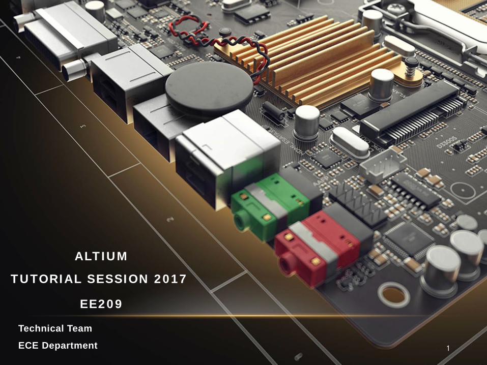
Technical Team
ECE Department
ALTIUM
TUTORIAL SESSION 2017
EE209
1

PCB
• Component placement
• Redefine Board Shape
• Mounting Holes
• Design Rules
• Routing
• Configuration
• Polygon Pour
• Design Rule Check (DRC)
STEPS OVERVIEW
2
Schematic
• New Project/File
• Add libraries
• Choose parts
• Wire/Bus
• Power/Ground/Net label
• Annotation/values
• Compile
Update PCB

NEW PROJECT/FILE• Start the Altium Designer Software. (Figure 1)• Ensure that the ‘Files’ and ‘Projects’ tabs are located somewhere on the screen. Most likely they will be minimized
on the left side of the window. If they are not then add them to the screena. View > Workspace Panels > System > Filesb. View > Workspace Panels > System > ProjectsAlternatively you may…(Figure 2)c. Click on the ‘System’ box in the lower right hand corner of the designer and then click ‘Files’ and ‘Projects’ to make the tabs appear.
These will both accomplish the same goal of making the ‘Files’ tab and the ‘Projects’ tabs visible. All tabs can be dragged and dropped nearly anywhere on the designer to suit your personal preferences.• Create a new PCB Project. File > New > Project > PCB Project – or – You may click on the ‘Files’ tab and then
under the ‘New’ heading you can click ‘Blank Project’ (Figure 3)This will cause the ‘Projects’ tab to open and ask to set the name of the project. We may want to change the name and location of our project otherwise it will save as ‘PCB1.PcbDoc’ in default location. (Figure 4)• We will now add a schematic and a PCB to the current project.
Right click on the project > Add New to Project > Schematic (Figure 5)Right click on the project > Add New to Project > PCB (Figure 6)
Finally, we should save the generated files:Right click on the name of each file>save (Figure 7,8,9)
3

ADD LIBRARIES
• Libraries are very important part of working with your schematic. Libraries are where all of your parts will be found and selected from. If you do not have the ‘Libraries’ tab anywhere on your screen you should…
Click the ‘System’ box in the bottom right portion of the designer and then click the ‘Libraries’ button. (Figure 10)
The Libraries panel enables you to browse and place components from the libraries currently available in Altium Designer• All components available in department store are listed and categorized according to their type in ECE Database library. For
a list of whole available components in ECE please see this webpage:
ECE Stock Inventory
And to add them to your project, you can find them in this path: (more information is available here)
S:\ECE\PCB_Libraries\ECE-Parts\ECEPart.DbLib
• Manufacturer libraries can be found in: S:\ECE\PCB_Libraries\Manufacturer-libraries
• The library we are going to use for EE209 is:
EE209.IntLib
• First download the library files from CANVAS and save them in your project folder then install it to Altium as shown below. Libraries can be added under Project tab or Installed tab.
i. Open library panel and select project tab. (Figure 14)
ii. Click on ‘add library’ button and find the downloaded library file in your project folder, click open.(Figure 15)
iii. You can see a list of your project libraries on the left side of the Altium page in projects tab.
iv. Run the same procedure to add “Database library” from S drive. (Figure 16)
13

SCHEMATIC PRACTICE
22

CHOOSE PARTS
• Add a resistor to your schematic page by following these steps (below image has red letters corresponding to the steps illustrated):
a. Make sure you have your schematics page opened
b. Open the ‘Libraries’ tab
c. Select the ‘EE209.IntLib’ library from the upper drop down (if this library is not in the drop down refer to previous step)
d. Type ‘Res’ into the dropdown textbox below the library listing
e. Make sure choosing proper foot print if there is more than one
f. Click the ‘Place Res’ button at the top of the libraries tab
g. Your cursor will then have a resistor attached to it and you can place it anywhere on the schematic
h. Once you have placed the resistor you can either hit the ‘Esc’ key –OR- right click your mouse to stop placing resistors
23
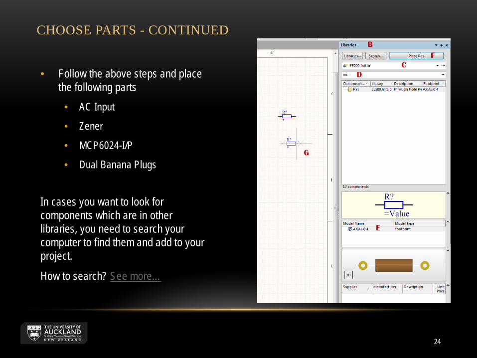
CHOOSE PARTS - CONTINUED
• Follow the above steps and place the following parts
• AC Input
• Zener
• MCP6024-I/P
• Dual Banana Plugs
In cases you want to look for components which are in other libraries, you need to search your computer to find them and add to your project.
How to search? See more…
24
B
CD
F
E
G

Notice: Some parts will need to be rotated and this can be accomplished by pressing the spacebar while you are placing the part or when the part is selected. Try to place the parts more or less like the following screenshot. Rotation is accomplished with the spacebar key while the mirror is added by right-clicking the part and checking the ‘mirrored’ checkbox. This does not make any difference on the PCB file it just makes your schematic easier to view and understand.
CHOOSE PARTS - CONTINUED
28
Notice: The unusedopamps should beproperly terminated. Ifconnected improperly, anuncommitted op amp leadsto problems such asincreased powerconsumption and addednoise.
OpAmp chips contains 4 opamps and unused ones needs to be disabled to avoid getting saturated.
Parts have been rotated using the spacebar key

WIRE/BUS
It is now time to wire theseparts together.
a. You can either click the‘Place Wire’ icon from the uppertoolbar or select Place > Wire.Both are illustrated here.
b. Once you click this icon yourcursor will turn into a crosshairwith a black X on it. Once youhover over a valid place toconnect a wire the X will turnred. If the X does not turn redwhen you place the wire aproper connection was notmade and this will lead toerrors later in the process.The red X is illustrated close uphere.
29
Use either of them to add wires
WIRE/BUS - CONTINUED
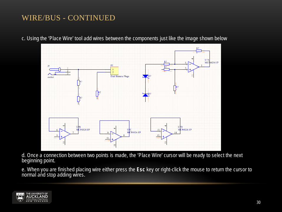
c. Using the ‘Place Wire’ tool add wires between the components just like the image shown below
d. Once a connection between two points is made, the ‘Place Wire’ cursor will be ready to select the next beginning point. e. When you are finished placing wire either press the Esc key or right-click the mouse to return the cursor to normal and stop adding wires.
30

POWER/GROUND/NET LABEL
• Now it’s time to add the Power and Ground nets to the schematic
a. Click the ‘VCC Power Port’ button that is next to the ‘Place Wire’ button and place them in the places shown in the image on the next page
i. ports will be renamed from ‘VCC’ to corresponding values. Naming ports is the same thing as connecting them with a wire but it is a more elegant solution for keeping the schematic less congested.
ii. To rename a port just double click on the port and its properties dialog box will pop up. You can then change the text in the ‘Net’ textbox in order to change the name of the net. Shown below.
31
POWER/GROUND/NET LABEL - CONTINUED
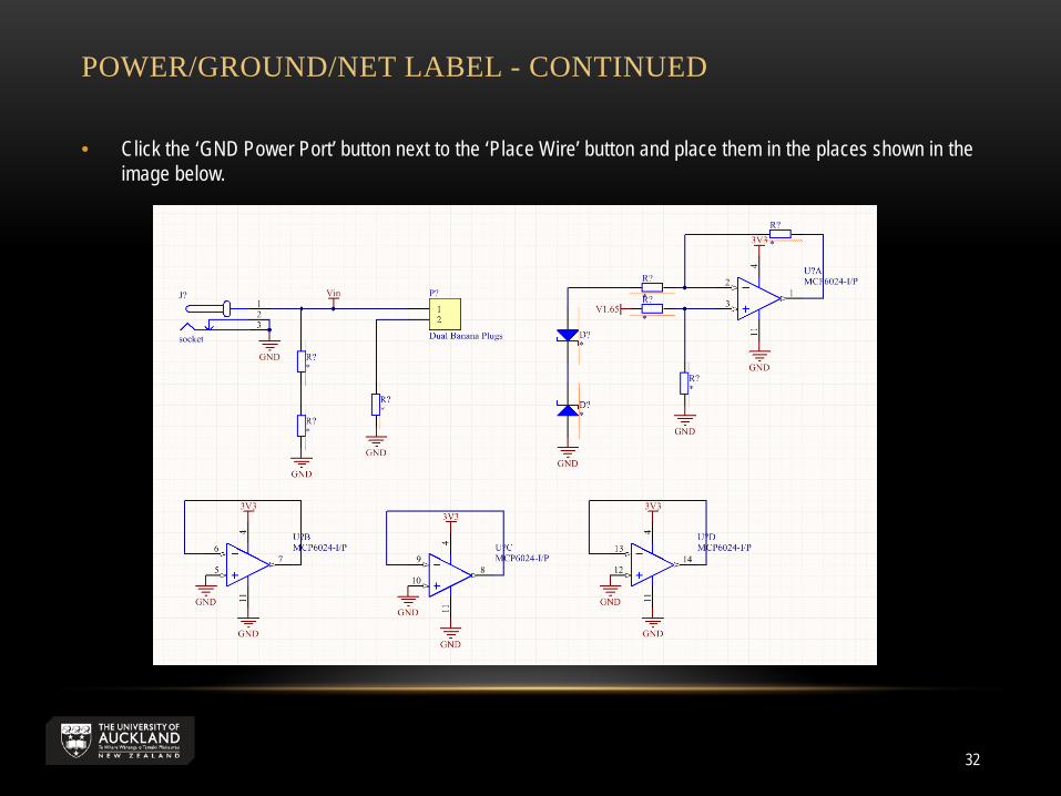
• Click the ‘GND Power Port’ button next to the ‘Place Wire’ button and place them in the places shown in the image below.
32

POWER/GROUND/NET LABEL - CONTINUED
• Now we will use named nets to add connections to our schematic without wires.a. Click on the ‘Place Net Label’ icon next to the place wire icon –OR- click Place > Net Label.b. Use spacebar to rotate the net label to make it easier to place.c. Make sure the red cross is appeared before you release net label.d. Place nets as shown in the image below.
e. In order to rename the net Double click it –OR- Right click and select Properties then change the value in the textbox for Net to ‘I_Sense’.
Note: make sure net label is connected properly. The grey cross should be red when attached to a point.
33
ANNOTATION
It is now time to annotate all of the unnamed components
a. Add more descriptive comments to the ports, this will make them easier to find on the PCB later
i. Double click on the AC input socket and Change the comment ‘=Value’ and make it say ‘AC Input Socket’
b. You can add text to your schematic to make it easier to understand.
Place Text String
c. No two components are allowed to have the same designator we must rename them; this can be accomplished one-by-one or can be done automatically
i. You can change designator of each component manually. Double click on the component and change the text in the Designator field (not recommended)
ii. –OR- You can do them all at once automatically using tools in Altium (much easier)
1. Tools > Annotation > Annotate Schematics Quietly
2. Click OK when the dialog box pops up to tell you how many changes will be made
3. This will automatically add unique designators to each component depending on the annotation rules that are currently in place
4. You may optionally change the annotation rules using Tools > Annotate Schematics if you want more control over the way the program decides to rename you designators for you. That is out of the scope of this tutorial
34

ANNOTATION
Your schematic looks like the one below without any question marks on it
35
Question marks are gone and
components have unique names
New port comments

VALUES
Now, we should change the “value” of each component according to our design.
• Double click on each component and change value parameter to the appropriate value and click OK.
• Make sure the comment is visible. (Figure 21). Your design would be similar to figure below.
36

COMPILE
Now the Schematic is ready and we can design the PCB file.
Before transferring to PCB, make sure your schematic design has no error.
in Project > Compile PCB project ‘nameOfProject.PrjPcb’
When the project is compiled, all warnings and errors will displayed in the Messages panel. The panel will only appear automatically if there are errors detected. If there are errors, work through each one, checking your circuit and ensuring that all wiring and connections are correct.
Here is a sample error message which is not for our project file.
38

FINAL SCHEMATIC
39

UPDATE PCB
We are now ready to update the PCB file
a. Design > Update PCB Document ‘nameOfProject.PcbDoc’
b. Scroll to the bottom of the window that pops up and uncheck the box next to the room that the program is trying to add
c. Click Validate Changes, make sure all of the changes get validated
d. Click Execute Changes, this will add all of the components and nets to your PCB document
e. Close the update window (Figure 23)
The PCB file should have automatically opened for you; if not, open it now
a. Click View > Fit Sheet to see the board as well as all of your components
b. You will notice that the components are added outside of the board area (black area)
c. The components can be dragged onto the board as you place them
40
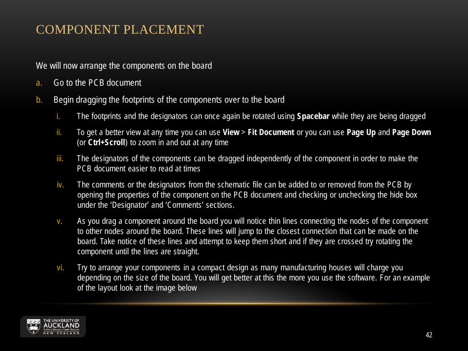
COMPONENT PLACEMENT
We will now arrange the components on the board
a. Go to the PCB document
b. Begin dragging the footprints of the components over to the board
i. The footprints and the designators can once again be rotated using Spacebar while they are being dragged
ii. To get a better view at any time you can use View > Fit Document or you can use Page Up and Page Down (or Ctrl+Scroll) to zoom in and out at any time
iii. The designators of the components can be dragged independently of the component in order to make the PCB document easier to read at times
iv. The comments or the designators from the schematic file can be added to or removed from the PCB by opening the properties of the component on the PCB document and checking or unchecking the hide box under the ‘Designator’ and ‘Comments’ sections.
v. As you drag a component around the board you will notice thin lines connecting the nodes of the component to other nodes around the board. These lines will jump to the closest connection that can be made on the board. Take notice of these lines and attempt to keep them short and if they are crossed try rotating the component until the lines are straight.
vi. Try to arrange your components in a compact design as many manufacturing houses will charge you depending on the size of the board. You will get better at this the more you use the software. For an example of the layout look at the image below
42

REDEFINE BOARD SHAPE
• Redefine the board shape (The black background on the screen is the board)
a. View > Board Planning Mode
b. a green screen will appear. Then go to Design > Redefine Board Shape
c. The cursor will turn into a crosshair
d. Zoom in to get a closer view of the grid and click the first corner of the new board shape that you want; continue to the next corner and click again; once you return to the first corner that you clicked on there will be a circle around the crosshair letting you know that you are back where you started; Once you are finished either Right-click or press Esc in order to stop redefining the board.
e. View > 2D Layout Mode. The board should look something like the image below
43
45
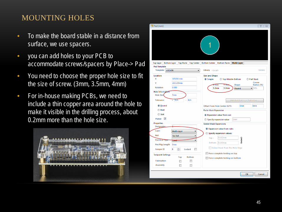
• To make the board stable in a distance from surface, we use spacers.
• you can add holes to your PCB to accommodate screws/spacers by Place-> Pad
• You need to choose the proper hole size to fit the size of screw. (3mm, 3.5mm, 4mm)
• For in-house making PCBs, we need to include a thin copper area around the hole to make it visible in the drilling process, about 0.2mm more than the hole size.
MOUNTING HOLES

DESIGN RULES
a. Open the rule wizard using Design > Rule
b. In the ‘Routing’ select ‘width’ and change the constraints to:
Min Width: 0.4 mm
Preferred Width: 1 mm
Max Width: 10 mm
46
Change the design rule of the board to define Track Width and Clearance

DESIGN RULES - CONTINUED
in ‘Electrical’ select
‘Clearance’ and change the
‘Minimum Clearance’ to 0.5mm
47
Change the design rule of the board to define Track Width and Clearance
ROUTING
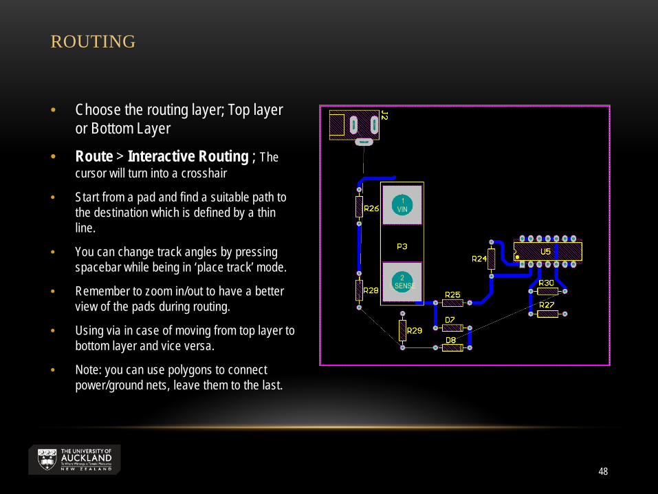
• Choose the routing layer; Top layer or Bottom Layer
• Route > Interactive Routing ; The cursor will turn into a crosshair
• Start from a pad and find a suitable path to the destination which is defined by a thin line.
• You can change track angles by pressing spacebar while being in ‘place track’ mode.
• Remember to zoom in/out to have a better view of the pads during routing.
• Using via in case of moving from top layer to bottom layer and vice versa.
• Note: you can use polygons to connect power/ground nets, leave them to the last.
48

CONFIGURATION
Add your initials and a revision numbera. Use Place > String to add the string to an empty space on your board
b. Double click the string to open its properties
i. Change the text field to your course name and group number
i.e. ‘Course name - Group number’
Add a keepout layer to the perimeter of your boardsome manufactures will use this to cut your board
a. Select ‘Keep-Out Layer’ from the tabs at the bottom of the designer window; up to this point we have been working from the ‘Bottom Layer’
b. Make sure the Keepout layer is selected then Add a Line using Place > Line. This will be similar to redefining the shape of the board where you can zoom in at the corners to make sure you are clicking the right spot and then zoom back out to get to the next corner more quickly.
c. Add the Line to the perimeter of the board and then press Esc to stop adding the track. The keepout Line should be pink because it is on the keepout layer.
49
POLYGON POUR
Polygon Pour is a way to make an area with a specific net name which is covered by copper and is used to make a bigger area than a wire with the same application.
Here, we are going to use it to make a ground area in both power side and digital side of the circuit. Normally we separate these two grounds with proper filtering, but in this tutorial example just simply connect two grounds together (see next page image)
After your PCB has been routed and you are ready to pour copper on the top and bottom layers:
• Click the “Place” tool bar button and select “PolyGon Pour…”.
• Set the layer to Bottom Layer and also set the “Connect to Net” to your ground net. Tick ‘Remove Dead copper’ then Click OK. (Fig.20)
• Your mouse pointer will change to a cross hair. Use this pointer to draw a shape similar to Fig. 23 .
• Do the same and make another shape and connect to Net ‘VIN’. Fig. 24
• And the third one should be named as ‘I_Sense’ Net. Fig. 25
• After drawing, right click your mouse to exit the draw mode.
50
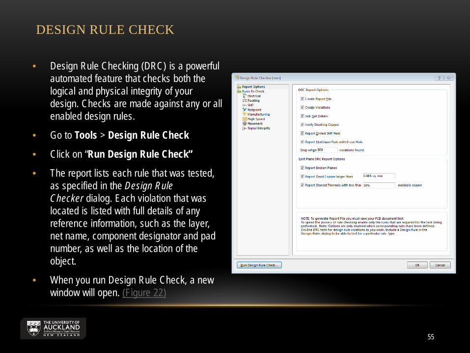
DESIGN RULE CHECK
55
• Design Rule Checking (DRC) is a powerful automated feature that checks both the logical and physical integrity of your design. Checks are made against any or all enabled design rules.
• Go to Tools > Design Rule Check
• Click on “Run Design Rule Check”
• The report lists each rule that was tested, as specified in the Design Rule Checker dialog. Each violation that was located is listed with full details of any reference information, such as the layer, net name, component designator and pad number, as well as the location of the object.
• When you run Design Rule Check, a new window will open. (Figure 22)
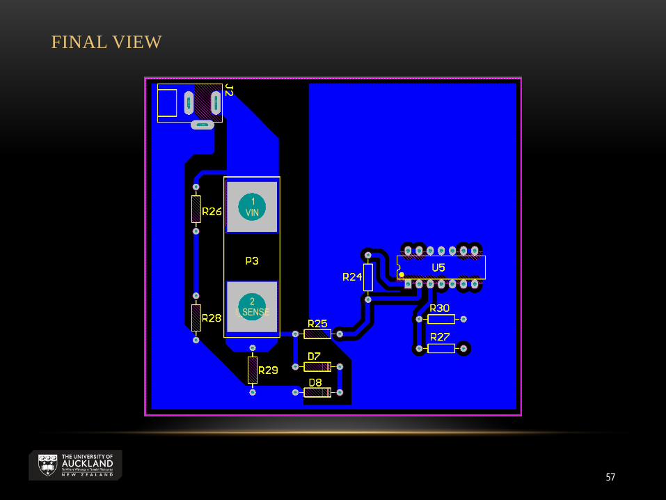
FINAL VIEW
57

ANY QUESTION?