Embed Size (px)
Citation preview

©Alex Doboli 2006
Switched Capacitor Blocks
Alex Doboli, Ph.D.
Department of Electrical and Computer Engineering
State University of New York at Stony Brook
Email: [email protected]

©Alex Doboli 2006
Overview of the Chapter
• Introduction to SC circuits
• Programmable SC blocks in PSoC
• SC principle: controlled movement of charge• Electrical nonidealities: circuit nonidealities, non-zero switch
resistance, channel charge injection, clock feedthrough • Basic SC blocks: gain amplifier, programmable gain amplifier,
comparator, integrator, differentiator• PSoC’s programmable SC blocks:
– Type C and Type D SC blocks
– Programming (registers)

©Alex Doboli 2006
Introduction to SC Techniques
• SC techniques:– Integrated capacitors are easier to fabricate than resistors– Average resistance approximated through charge movement
I = V / R
Q = C V
Iaverage = Q fs = C V fs => Req = 1 / C fs

©Alex Doboli 2006
Introduction to SC Techniques
• Constraints:– Switches Ф1 and Ф2 can never be closed at the same time
– Switch Ф1 must have time to open before switch Ф2 closes
– Switch Ф2 must have time to open before switch Ф1 closes
– Frequency fs must allow enough time for the circuits to fully charge and discharge

©Alex Doboli 2006
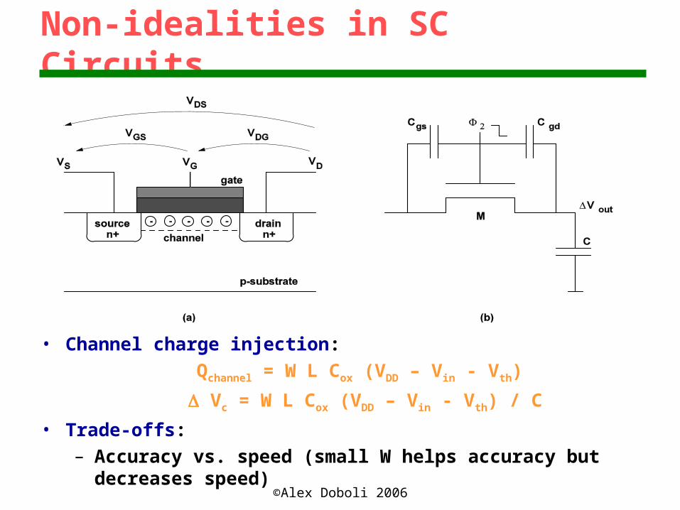
Non-idealities in SC Circuits
• Non-zero on-resistance of MOSFETs:
d Vc(t) / d t = ID(t) / C
Linear: d Vc(t) / d t = Cox W [(VDD – Vc(t) - Vth)(Vin – Vc(t)) – (Vin – Vc(t))2 / 2] / 2 LC
Vc(t) = 2 K exp (A Vin t) – A exp (A Vin t) + exp (kt + K[1]))Vin /
(A exp (A Vin t) + exp (K t + K[1])
A = Cox W / 2 L C
K = A (VDD – Vth)
Saturation:d Vc(t) / d t = Cox W [(VDD – Vc(t) - Vth)(Vin – Vc(t)) – (Vin – Vc(t))2 / 2] / 2 LC
Vc(t) = [(A t – C[1]) (VDD - Vth) - 1] / (A t – C[1])
Vc(0) = 0 => C[1] = - 1 / (VDD - Vth)
Vc(t) = VDD – Vth – 1 / (a t – C[1])
©Alex Doboli 2006
Non-idealities in SC Circuits
• Channel charge injection:
Qchannel = W L Cox (VDD – Vin - Vth)
Vc = W L Cox (VDD – Vin - Vth) / C
• Trade-offs: – Accuracy vs. speed (small W helps accuracy but decreases
speed)
©Alex Doboli 2006
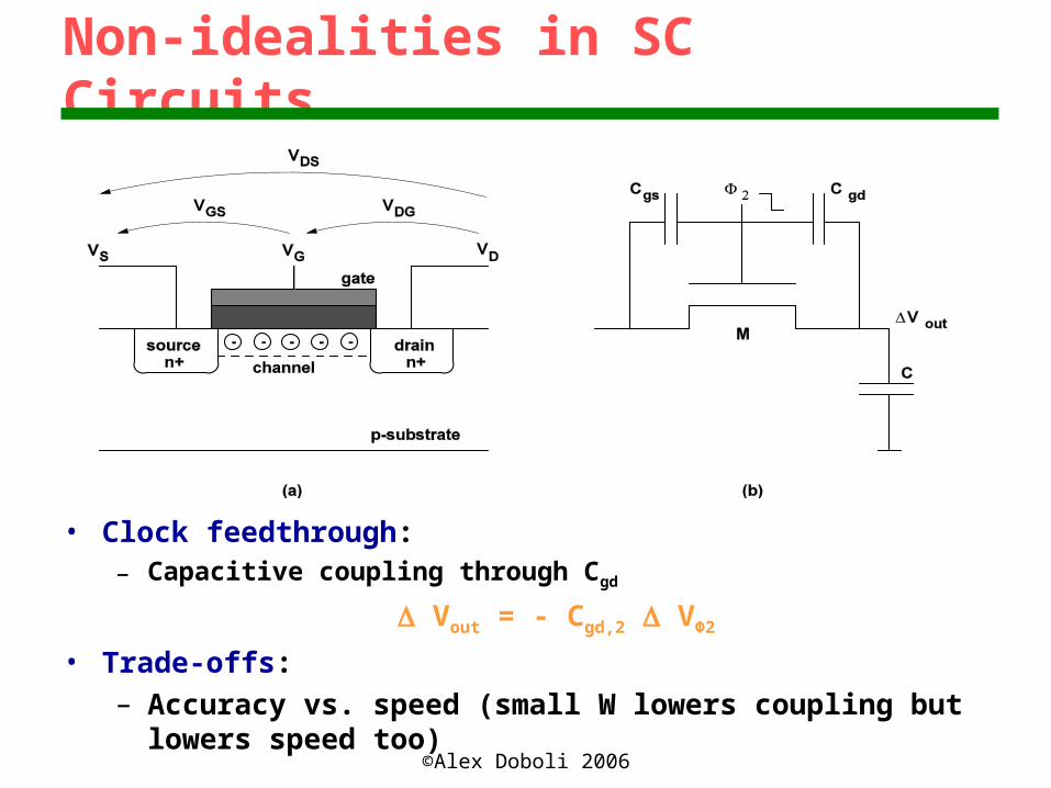
Non-idealities in SC Circuits
• Clock feedthrough:– Capacitive coupling through Cgd
Vout = - Cgd,2 VΦ2
• Trade-offs: – Accuracy vs. speed (small W lowers coupling but lowers
speed too)

©Alex Doboli 2006
SC Fixed Gain Amplifier
Characteristics:• acquisition phase• transfer phase
©Alex Doboli 2006
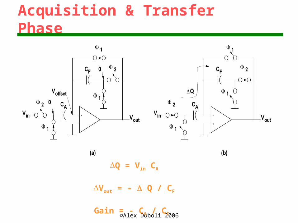
Acquisition & Transfer Phase
Q = Vin CA
Vout = - Q / CF
Gain = - CA / CF

©Alex Doboli 2006
Autozero Adjustment
QAi = Voffset CA
QFi = Voffset CF
QAf = (Vin – Voffset) CA
QFf = (Voffset – Vout
f) CF
QAi + QF
i = QAf + QF
f
Voutf = Voffset – [(CA + CF) Voffset –
CA(Voffset - Vin)] / CF
Voutf = - CA / CF Vin

©Alex Doboli 2006
SC Selectable Gain Polarity Amplifier

©Alex Doboli 2006
SC Comparator

©Alex Doboli 2006
SC Integrator

©Alex Doboli 2006
SC Integrator
During acquisition: Q = Vin CA
During transfer: Qtot = Q’ + Vin CA
Vout (t) = Vout (t – Ts) + CA / CF Vin
[Vout (t) - Vout (t – Ts)] / Ts = fs CA / CF Vin
d Vout (t) / dt = CA / CF fs Vin
Integrator gain: CA / CF fs

©Alex Doboli 2006
SC Differentiator

©Alex Doboli 2006
Improved Reference Selection
©Alex Doboli 2006
Improved Reference Selection
Ground reference: Vout = Vin CA / CF
Vref+ reference: Vout = (Vin – Vref+) CA / CF
Vref- reference: Vout = (Vin – Vref-) CA / CF
Integrator gain: CA / CF fs

©Alex Doboli 2006
Two Bit ADC

©Alex Doboli 2006
Two Bit ADC
1. Vin > Vref+
2. Vin < Vref+ and Vin > 03. Vin < 0 and Vin > Vref-
4. Vin < Vref-
©Alex Doboli 2006
Analog to Digital Conversion
©Alex Doboli 2006
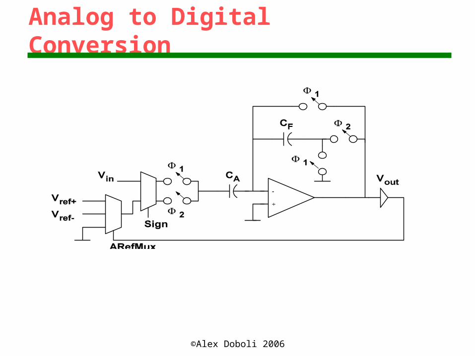
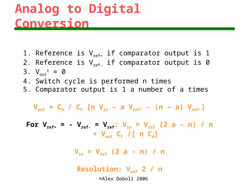
Analog to Digital Conversion
1. Reference is Vref+ if comparator output is 12. Reference is Vref- if comparator output is 03. Vout
i = 04. Switch cycle is performed n times5. Comparator output is 1 a number of a times
Vout = CA / CF [n Vin – a Vref+ - (n – a) Vref-]
For Vref+ = - Vref- = Vref: Vin = Vref (2 a - n) / n + Vout CF /[ n CA]
Vin = Vref (2 a - n) / n
Resolution: Vref 2 / n
©Alex Doboli 2006
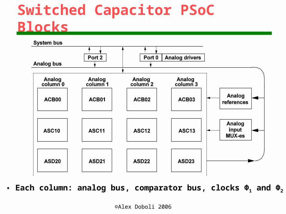
Switched Capacitor PSoC Blocks
• Each column: analog bus, comparator bus, clocks Φ1 and Φ2

©Alex Doboli 2006
PSoC Type C Block

©Alex Doboli 2006
PSoC Type C Block
1. Control registers: ASCxxCR0, ASCxxCR1, ADCxxCR2, ASCxxCR31. Functionality (gain, integrator, comparator)2. Input & output configuration3. Power mode4. Sampling procedure (positive / negative gain)
2. OpAmp: 1. 4 power modes (off, low, medium, high)2. Programmed through bits PWR (bits 1-0 of ASCxxCR3)3. Functionality programmed through bits FSW1 and FSW0
3. Bit FSW1:1. FCap connected or not (gain/integrator or comparator) 2. Bit 5 of ASCxxCR3
4. Bit FSW0:1. FCap discharged or not (gain or integrator)2. Bit 4 of ASCxxCR3

©Alex Doboli 2006
PSoC Type C Block
5. Programmable matrix arrays: ACap, BCap, CCap, FCap1. ACap value programmed through bits 4-0 of ASCxxCR02. Value: 0 – 31 units (1 unit ~ 50fF)3. Autozero bit:
1. Autozeroing during Φ1
2. Bit 5 of ASCxxCR24. Asign bit: positive or negative gain
1. Bit 5 of ASCxxCR02. Positive gain: input sampled on clock Φ1
3. Negative gain: input sampled on clock Φ2
4. Reference selection6. BCap:
BCap capacitor value: 0 – 31 units Bits 4 – 0 in ASCxxCR1
7. CCap:1. CCap capacitor value: 0 – 31 units 2. Bits 4-0 in ASCxxCR2

©Alex Doboli 2006
PSoC Type C Block
8. FCap: Value programmed through bit 7 of ASCxxCR0 Value: 16 or 32 units
9. Programmable inputs: 1. Inputs to ACap, BCap, CCap are programmable
1. Bits 7-5 of ASCxxCR12. Reference to ACap is also programmable
1. Bits 7-6 of ASCxxCR32. AGND, Vref+, Vref-, comparator output (RefHi if
comparator output is high, and RefLo if comparator output is low)
©Alex Doboli 2006
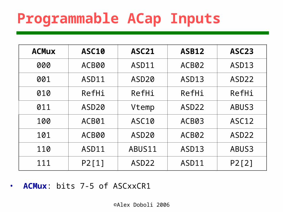
Programmable ACap Inputs
ACMux ASC10 ASC21 ASB12 ASC23
000 ACB00 ASD11 ACB02 ASD13
001 ASD11 ASD20 ASD13 ASD22
010 RefHi RefHi RefHi RefHi
011 ASD20 Vtemp ASD22 ABUS3
100 ACB01 ASC10 ACB03 ASC12
101 ACB00 ASD20 ACB02 ASD22
110 ASD11 ABUS11 ASD13 ABUS3
111 P2[1] ASD22 ASD11 P2[2]
• ACMux: bits 7-5 of ASCxxCR1

©Alex Doboli 2006
Programmable BCap Inputs
BCMux ASC10 ASC21 ASB12 ASC23
00 ACB00 ASD11 ACB02 ASD13
01 ASD11 ASD20 ASD13 ASD22
10 P2[3] ASD22 ASD11 P2[0]
11 ASD20 TrefGND ASD22 ABUS3
• BCMux: bits 3-2 of ASCxxCR3

©Alex Doboli 2006
Programmable CCap Inputs
ACMux ASC10 ASC21 ASB12 ASC23
000 ACB00 ASD11 ACB02 ASD13
001 ACB00 ASD11 ACB02 ASD13
010 ACB00 ASD11 ACB02 ASD13
011 ACB00 ASD11 ACB02 ASD13
100 ASD20 ASD11 ASD22 ASD13
101 ASD20 ASD11 ASD22 ASD13
110 ASD20 ASD11 ASD22 ASD13
111 ASD20 ASD11 ASD22 ASD13
• ACMux: bits 7-5 of ASCxxCR1

©Alex Doboli 2006
PSoC Type C Block
10. Programmable outputs: 1. Bit AnalogBus:
1. Output to analog buffer2. Bit 7 of ASCxxCR2
2. Bit CompBus:1. Connects comparator output to digital block inputs2. Bit 6 of ASCxxCR2
11. Clocking scheme: 1. Bit ClockPhase:
1. Bit 6 of ASCxxCR02. External Φ1 or Φ2 is internal Φ1
©Alex Doboli 2006
Type D Switched Capacitor Blocks

©Alex Doboli 2006
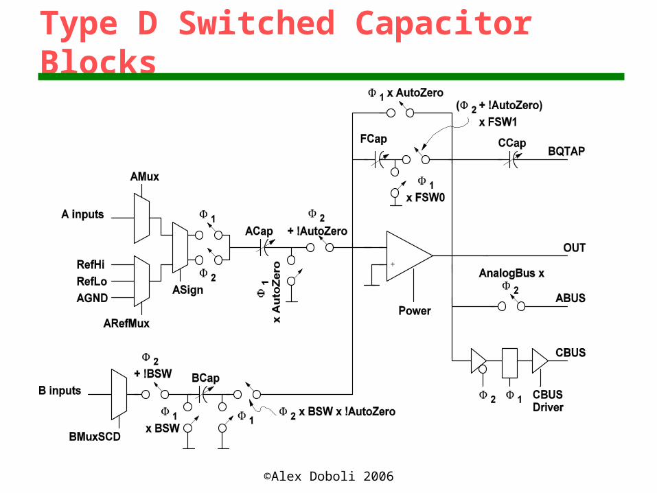
Type D Switched Capacitor Blocks
Differences:
CCap connected to the output, which connects to the suming node of the next SC C block (biquad filters)
Switch BSW: BCap is either SC or fixed capacitor BCap connected to the summing node AnalogBus switch connects OpAmp output to analog buffer CompBus switchconnects comparator to the digital blocks BCap programmable capacitor sampled on Φ2

©Alex Doboli 2006
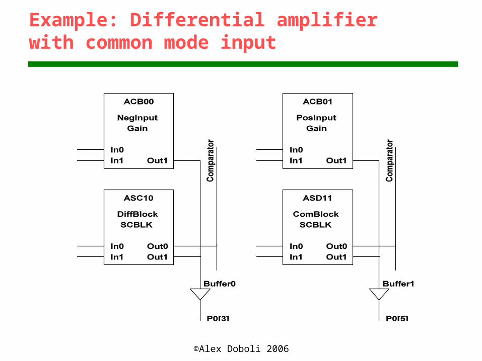
Example: Differential amplifier with common mode input
Vdifferential = PosInput – NegInputVcommon = (PosInput + NegInput) / 2
©Alex Doboli 2006
Example: Differential amplifier with common mode input

©Alex Doboli 2006
Analog to Digital Conversion

©Alex Doboli 2006
Isolated Analog Driver