Embed Size (px)
Citation preview
Digital Alarm ClockE157 Final Project
Final Report
Jason FongFernando Mattos
Abstract:
Digital alarm clocks typically use 7-segment LED’s as its display, and a count-up schemefor changing the clock time and alarm times. With the availability of a twelve keykeypad and LCD screen, a simple alarm clock can look much sharper, and work muchbetter. Such a clock is constructed by combining the E157 FPGA board with the HC11to control and generate the keypad inputs and LCD display outputs. The FPGA and theon board clock oscillator will generate accurate timing signals and debounce keypadinputs, while the HC11 will store the time value, handle alarm clock functions, andgenerate the control signals to the LCD. The audible alarm will simply be a square wavesignal generated by the FPGA amplified by a set of external computer speakers.
Introduction
The motivations behind the choice of the alarm clock as a final project are the
following: its utilization of both the FPGA and the HC11, its use of an LCD display, and,
finally, its advantages over a conventional digital alarm clock.
The final project requirements are met by the tasks required of both components.
The HC11’s memory capabilities is used to store and increment time information, while
its capability to perform more complex sequential tasks streams the functions such as
changing into an editing mode for time editing, etc. The FPGA board uses an external
oscillator that generates accurate clock speeds. This fact makes the FPGA an ideal
choice for generating accurate timing signals. The FPGA also handles the debouncing of
the keypad input since the procedure is best handled by permanent logic. In short, both
components are important counterparts of each other for the alarm clock.
In addition to being a suggested component for a final project, the LCD screen is
a great component for the purposes of displaying numbers and characters. The LCD
screen’s ability to display multiple characters allows for a friendlier menu-type display,
replacing the various primitive methods of entering data into alarm clocks. Furthermore,
the LCD display has on-board display memory and built-in character display functions
(cursor position, pre-programmed characters, etc.). These features make the HC11 the
single necessary component to drive the LCD display.
The LCD display digital alarm clock provides several advantages over regular
alarm clocks. These advantages include having keypad input instead of the single-button
up-counting input for commercial alarm clocks, and using an LCD screen for a sleeker
display.
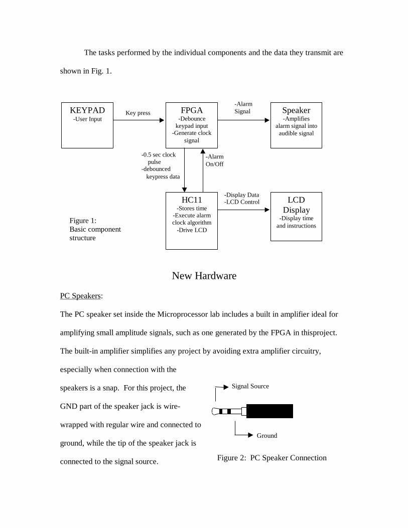
The tasks performed by the individual components and the data they transmit are
shown in Fig. 1.
New Hardware
PC Speakers:
The PC speaker set inside the Microprocessor lab includes a built in amplifier ideal for
amplifying small amplitude signals, such as one generated by the FPGA in thisproject.
The built-in amplifier simplifies any project by avoiding extra amplifier circuitry,
especially when connection with the
speakers is a snap. For this project, the
GND part of the speaker jack is wire-
wrapped with regular wire and connected to
ground, while the tip of the speaker jack is
connected to the signal source.
HC11-Stores time
-Execute alarmclock algorithm
-Drive LCD
LCDDisplay
-Display timeand instructions
KEYPAD-User Input
FPGA-Debounce
keypad input-Generate clock
signal
Speaker-Amplifies
alarm signal intoaudible signal
Key press
-0.5 sec clock pulse-debounced keypress data
-Display Data-LCD Control
-AlarmOn/Off
-AlarmSignal
Figure 1:Basic componentstructure
Ground
Signal Source
Figure 2: PC Speaker Connection
LCD Display:
The LCD display unit comes with a multitude of support circuitry on-board. The
tasks of refreshing the LCD screen, temporary storing display information, character
information, etc. are all handled by the memory and microcontrollers provided. The task
of writing to the LCD becomes therefore a strict regime of following the manufacturer’s
directions.
Connections to the LCD display unit are made through the 14 pins on the board.
The pin symbols are provided in both Appendix X and the spec sheets provided by the
manufacturer.
The Vee pin provides power for the display unit itself. An exterior potentiometer
is used to keep this voltage between the maxim of 5V (Vcc) and the low voltage.
Adjusting this value effectively adjusts the contrast of the LCD display. If a
potentiometer is not available, simply connecting the Vee pin to Vcc should suffice for
testing purposes.
The RS pin is the “Register Select Signal.” When driven high, the LCD unit will
expect to receive data information. While low, the LCD unit will expect instruction
input.
The R/W pin stands for Read or Write. When high, the LCD unit expects an
instruction or data input into the system. When low, the LCD unit will actually send
status information out to the controlling microcontroller. The write function was not
utilized in this project.
The E pin is where the Enable signal is sent. This enable signal is the timing
control for any information transfer in or out of the LCD unit. The enable cycle time
must be a minimum of 500 ns. As long as instruction transfer does not exceed 2MHz,
information transfer should not be a problem. Like enable pins of other devices, pulling
the enable pin high causes the LCD unit to read the data pins for information. The
microcontroller should write data ports before pulling the enable pins high.
A intializing sequence must be followed for the LCD screen to start properly.
The sequence provided by the manufacturers did not function properly or consistently, so
an alternate sequence was used in its place.
Once initialized, the LCD unit is ready to receive data from the microcontroller.
The LCD unit performs functions such as locating the cursor, flashing the cursor, etc.
depending on the instruction it receives. When data is received instead of instructions, the
LCD unit simply prints the character represented by the data at the cursor’s current
location.
Component Connections
The prototype alarm clock uses a solderless breadboard with basic 22wg wiring.
Each component have pins which are numbered by manufacturer, or are noted in the
diagrams below. The connections between pins are provided in appendix A.
At the board level, most of the wiring are direct connections between component
pins. The exceptions to this fact are the LCD’s display power, Vee, which requires an
external potentiometer to function, and the speaker connection, which is simply wire
wrapped around the speaker connector jack. The potentiometer hookup for Vee is
discribed in appendix A also.

Since very few external circuit components are used, a schematic of the
component connections will not be provided here. Figure 1 is representative of what the
schematics will look like, while Appendix A will provide sufficient pin-out information
for the connecting wires.
Microcontroller Design
The HC11 microcontroller is responsible for the following tasks: storing of the
actual time, incrementing the time, sending control and display data to the LCD screen,
sending the alarm on/off signal, receiving input information from the FPGA, and
maintaining the main program loop that calls upon various subroutines according to the
input. The main loop handles each task separately through subroutines specific to each
task. Each subroutines may use additional function routines that perform special LCD
display functions. The following sections describe the software program structure and
the input/output port assignments.
Program Structure:
Initialization:- Clear variables- Clear Port A and E- Handshake with FPGA- Reset Clock, Alarm, and Snooze time to 00:00:00- Call on subroutine to clear LCD routine
Main Program Loop:- Jump to subroutine described by MODE variable- Default to standard mode (MODE0)- Restart Main program loop
MODE subroutines:- MODE0 (Standard mode)
- Call on function routine to draw “Standard” screen- Loop until E (exit) key pressed
- Call on function to get input from FPGA- Update Time if time change- Update Time on display- Check to see if Alarm triggered
- Write MODE variable and return to Main Program Loop if key pressed- MODE1 (Time Edit mode)
- Call on function routine to draw “Time Edit” screen- Call on “EDIT” function routine- Return to Main Program Loop
- MODE2 (Alarm mode)- Calls on function routine to draw “Alarm Edit” screen- Loop until E (Edit) or F (exit) key pressed
- Call on function routine to get input from FPGA- Call on function routine to update alarm time- Call on function routine to print new alarm time on screen- Toggles alarm state if key press is A
- Write MODE variable and returns to Main Program Loop- MODE3 (Alarm Edit mode)
- Call on function routine to draw “Alarm Edit” screen- Call on EDIT function routine- Call on function routine to set snooze time to alarm time- Returns to MODE 2
The remainder of the microcontroller code are the function routines which perform
specific tasks such as moving the LCD cursor, or a write to a Time register, etc. Refer to
the code provided in the appendix for more information on these function routines.
FPGA Design
The FPGA is mapped using the Verilog HDL. A total of 5 modules are used. The
following sections describe each module separately.
Main.v:Inputs: master_clock, row_data, soundOutputs: col_data, number, sclock, change, so_clk
The main module is the top level module responsible for I/O to other components andwiring between sub-modules.
The master_clock signal is generated by an external oscillator. This signal is also theprimary clock for the FPGA. With the exception to the number bus and change pin,all other I/O busses and pins are directly connected to sub-modules.
The 4-bit wide number bus and the change pin is connected to registers that updatewith every key press. The number register updates to hold the value of the last keypressed, while the change register inverts its value. The change pin works as asimple handshaking method for communication with the HC11. Since the numberregister always retains the value of the last key pressed, only a change in the valueheld by the change register will the HC11 recognize the key data as new.
Aux_Clock.v:Input: mclkOutput: aux_clk
This module generates a auxiliary clock signal which has a cycle time equal to 20,000cycles of the FPGA’s primary clock. The mclk pin connects to the master_clock pin,while aux_clk outputs the generated clock signal to other modules.
The clock divider signal is obtained by using a finite state machine that increments a14-bit register every mclk cycle when the register is less than a decimal value of10,000, at which point the FSM resets the value of the register and restarts.
Keypad_Scan.v:Input: aux_clk, rowOutput: col, key_pressed, data_out
The Keypad_Scan module performs two tasks. First, it scans and debounces thekeypad inputs. Second, it decodes any key press into its binary representationrecognizable by the HC11’s algorithm.
Keypad scanning is done by alternating pulses sent to each column of the matrixkeypad, then reading to see if any keypad row is shorted with the column in question.By identifying the row and columns where the short occurred, it’s then possible todistinguish one key from another.
The scanning procedure uses a finite state machine. In the starting state, the output tothe keypad columns cycles through with every aux_clk cycle. When a row valuechange is detected that value is stored and the finite state machine enters the secondstate (pause state). The second state is simply a pause necessary to debounce a signal.The machine enters the third state at the next clock cycle. If the row value stored hasnot changed (key is still pressed), the machine decodes the signal and returns to theoriginal state.
S_Clock.v:Input: mclkOutput: s_clk
This module is the same as the aux_clk module with the exception that the clockdivider counts up to 500,000 to generate a clock signal with a 1 second period. Thegenerated signal is the signal used to increment the actual time value on the HC11.
Sound_Clk.vInput: mclk, soundOutput: so_clk
This module generates the sound signal sent to the computer speakers. The modulenearly the same as aux_clk module, but with a divisor of 500 to generate a 1kHzsignal, and also the generate signal is “AND’ed” with a sound. The sound wireeffectively serves as a switch to turn the output signal on and off.
Results
The alarm clock worked as planned. All the important aspects of a good alarm
clock – its timing accuracy, functionality, ease of use, etc are all represented in the final
prototype. The LCD alarm clock even feature a user-friendly menu system for time
changes. In short, all the goals set during the planning of this project were met. The only
difficulty in the project occurred when the manufacturer’s initialization sequence failed to
work. This was fixed by using another algorithm provided by internet resources.
References
1. Burian, Christopher J. “LCD Technical FAQ”,http://www.repairfaq.org/filipg/LINK/F_Tech_LCD.html, 1996
2. “LCD (programming & pinouts)”,http://www.repairfaq.org/filipg/LINK/F_LCD_progr.html, 1996
* Additional sources for LCD projects can be found at http://www.eio.com/lcdintro.htm

Parts List
1. LCD Module Engineering Stockroom2. PC Speakers Microprocessor Lab
APPENDIX AComponent Pinouts
L = LCD DisplayF = FPGA BoardH = HC11K = KeypadS = Computer External Speakers
1. LCD
L1 GND GNDL2 Vcc +5VL3 Ve see Figure 3L4 RS H28L5 R/W H29L6 E H30L7 Data 0 H42L8 Data 1 H41L9 Data 2 H40L10 Data 3 H39L11 Data 4 H38L12 Data 5 H37L13 Data 6 H36L14 Data 7 H35
2. FPGA
F13 MCLK ClockF38 row 0 K1F39 row 1 K4F40 row 2 K5F44 row 3 K3F45 col 3 K8F46 col 2 K7F47 col 1 K6F48 col 0 K2F72 number 0 H44F77 number 1 H49F78 number 2 H47F79 number 3 H45F81 change H46F82 sclock H43F83 so_clk S3F84 sound H27
GND
Ve
Vcc
Figure 3Vee Hookup
3. Keypad
K1 row 0 F38K2 col 0 F48K3 row 3 F44K4 row 1 F39K5 row 2 F40K6 col 1 F47K7 col 2 F46K8 col 3 F45
4. Computer External Speakers
S1 GND GroundS2 L Speaker Not UsedS3 R Speaker F83

APPENDIX B
HC11 ASM Code
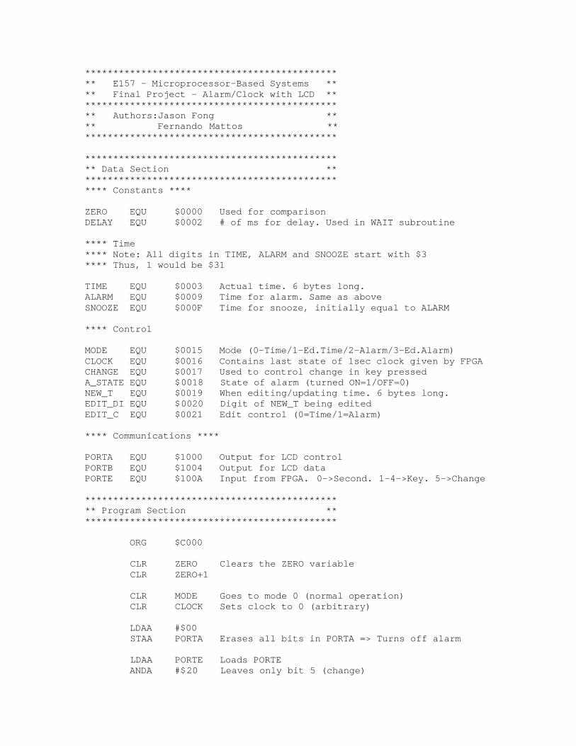
*********************************************** E157 - Microprocessor-Based Systems **** Final Project - Alarm/Clock with LCD ************************************************* Authors:Jason Fong **** Fernando Mattos ***********************************************
*********************************************** Data Section *************************************************** Constants ****
ZERO EQU $0000 Used for comparisonDELAY EQU $0002 # of ms for delay. Used in WAIT subroutine
**** Time**** Note: All digits in TIME, ALARM and SNOOZE start with $3**** Thus, 1 would be $31
TIME EQU $0003 Actual time. 6 bytes long.ALARM EQU $0009 Time for alarm. Same as aboveSNOOZE EQU $000F Time for snooze, initially equal to ALARM
**** Control
MODE EQU $0015 Mode (0-Time/1-Ed.Time/2-Alarm/3-Ed.Alarm)CLOCK EQU $0016 Contains last state of 1sec clock given by FPGACHANGE EQU $0017 Used to control change in key pressedA_STATE EQU $0018 State of alarm (turned ON=1/OFF=0)NEW_T EQU $0019 When editing/updating time. 6 bytes long.EDIT_DI EQU $0020 Digit of NEW_T being editedEDIT_C EQU $0021 Edit control (0=Time/1=Alarm)
**** Communications ****
PORTA EQU $1000 Output for LCD controlPORTB EQU $1004 Output for LCD dataPORTE EQU $100A Input from FPGA. 0->Second. 1-4->Key. 5->Change
*********************************************** Program Section ***********************************************
ORG $C000
CLR ZERO Clears the ZERO variable CLR ZERO+1
CLR MODE Goes to mode 0 (normal operation) CLR CLOCK Sets clock to 0 (arbitrary)
LDAA #$00 STAA PORTA Erases all bits in PORTA => Turns off alarm
LDAA PORTE Loads PORTE ANDA #$20 Leaves only bit 5 (change)
STAA CHANGE Sets CHANGE to the value at the FPGA
LDAA #$30 Resets TIME, ALARM and SNOOZE to 00:00:00 STAA TIME STAA ALARM STAA SNOOZE STAA TIME+1 STAA ALARM+1 STAA SNOOZE+1 STAA TIME+2 STAA ALARM+2 STAA SNOOZE+2 STAA TIME+3 STAA ALARM+3 STAA SNOOZE+3 STAA TIME+4 STAA ALARM+4 STAA SNOOZE+4 STAA TIME+5 STAA ALARM+5 STAA SNOOZE+5
JSR INITDR Initialization of LCD driver JSR CLEAR Clear LCD screen JSR CUR_OFF Turns cursor OFF
MLOOP LDAA MODE Checks which mode of operation is active CMPA #$00 BNE M1 JSR MODE0 Mode 0 - Show time JMP ENDLOOPM1 CMPA #$01 BNE M2 JSR MODE1 Mode 1 - Edit time JMP ENDLOOPM2 CMPA #$02 BNE M3 JSR MODE2 Mode 2 - Show alarm JMP ENDLOOPM3 CMPA #$03 BNE NONE JSR MODE3 Mode 3 - Edit Alarm JMP ENDLOOPNONE CLR MODE Default -> Go to mode 0ENDLOOP JMP MLOOP
SWI
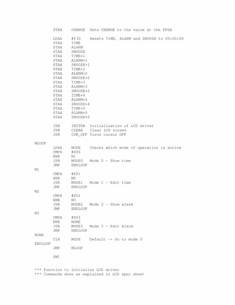
*** Function to initialize LCD driver*** Commands done as explained in LCD spec sheet
ORG $C100INITDR LDAA #$38 JSR WRITEC LDAA #$38 JSR WRITEC LDAA #$38 JSR WRITEC LDAA #$06 JSR WRITEC LDAA #$0C JSR WRITEC RTS
*** Function to write control information to LCD*** Control data in register A ORG $C180WRITEC* Bit 5 -> R/W, Bit 4 -> RS, Bit 3 -> E LDAB PORTA ANDB #%11000111 R/W=0,RS=0,E=0 STAB PORTA STAA PORTB Write controls LDAB PORTA ANDB #%11001111 ORAB #%00001000 R/W=0,RS=0,E=1 STAB PORTA LDAB PORTA ANDB #%11000111 R/W=0,RS=0,E=0 STAB PORTA LDAB PORTA ANDB #%11100111 R/W=1,RS=0,E=0 ORAB #%00100000 STAB PORTA LDAA #10 Delay for 10ms STAA DELAY JSR WAIT RTS
*** Function to write character data to LCD*** Character data in register A ORG $C200WRITED LDAB PORTA ANDB #%11010111 R/W=0,RS=1,E=0 ORAB #%00010000 STAB PORTA STAA PORTB Write character LDAB PORTA ANDB #%11011111 R/W=0,RS=1,E=1 ORAB #%00011000 STAB PORTA LDAB PORTA ANDB #%11010111 R/W=0,RS=1,E=0 ORAB #%00010000 STAB PORTA LDAB PORTA
ANDB #%11110111 R/W=1,RS=1,E=0 ORAB #%00110000 STAB PORTA LDAA #2 Delay for 2ms STAA DELAY JSR WAIT RTS
*** Function to clear LCD screen ORG $C280CLEAR LDAA #$01 JSR WRITEC RTS
*** Function to turn cursor on ORG $C300CUR_ON LDAA #$0D JSR WRITEC RTS
*** Function to turn cursor off ORG $C380CUR_OFF LDAA #$0C JSR WRITEC RTS
*** Function to move cursor one space to left ORG $C400CUR_LEFT LDAA #$10 JSR WRITEC RTS
*** Function to move cursor one space to right ORG $C480CUR_RIGHT LDAA #$14 JSR WRITEC RTS
*** Function to move cursor to a column in row 1*** Column in register A ORG $C500CUR1 DECA ADDA #$80 JSR WRITEC RTS
*** Function to move cursor to a column in row 2*** Column in register A ORG $C580CUR2 DECA
ADDA #$C0 JSR WRITEC RTS
*** Function to move cursor to a column in row 3*** Column in register A ORG $C600CUR3 DECA ADDA #$94 JSR WRITEC RTS
*** Function to move cursor to a column in row 4*** Column in register A ORG $C680CUR4 DECA ADDA #$D4 JSR WRITEC RTS
*** Function to move cursor home (0,0) ORG $C700HOME LDAA #$02 JSR WRITEC RTS
*** Operation Mode 0 ORG $C780MODE0 JSR SCREEN0 Draw screen for mode 0
LOOP0 JSR GINPUT Update time and get input. A=Key. B<>0 forkeypress PSHA PSHB JSR TIME2NEWT JSR PRTIME Print time JSR CK_ALARM CMPB #$00 BNE M01 Redraws screen PULB PULA CMPB #$00 BEQ LOOP0 No key pressed... keep waiting
CMPA #$0A BNE M0KE LDAA #$02 STAA MODE JMP ENDM0M0KE CMPA #$0E BNE LOOP0
LDAA #$01 STAA MODE JMP ENDM0
M01 PULB PULA JMP MODE0
ENDM0 RTS
*** Draw screen for mode 0 ORG $C900SCREEN0 JSR CLEAR
LDAA #8 "Time" on col 8, row 1 JSR CUR1 LDAA #$54 JSR WRITED LDAA #$69 JSR WRITED LDAA #$6D JSR WRITED LDAA #$65 JSR WRITED
LDAA #6 "Alarm" on col 6, row 3 JSR CUR3 LDAA #$41 JSR WRITED LDAA #$6C JSR WRITED LDAA #$61 JSR WRITED LDAA #$72 JSR WRITED LDAA #$6D JSR WRITED
LDAA #12 "ON" or "OFF" on col 12, row 3 JSR CUR3 LDAA #$4F JSR WRITED LDAA A_STATE CMPA #$01 BNE S0_AOFF Alarm is OFF LDAA #$4E JSR WRITED JMP S0_1S0_AOFF LDAA #$46 JSR WRITED LDAA #$46 JSR WRITEDS0_1
LDAA #1 "E-Edit" JSR CUR4 LDAA #$45 JSR WRITED LDAA #$B0 JSR WRITED LDAA #$45 JSR WRITED LDAA #$64 JSR WRITED LDAA #$69 JSR WRITED LDAA #$74 JSR WRITED
LDAA #14 "A-Alarm" JSR CUR4 LDAA #$41 JSR WRITED LDAA #$B0 JSR WRITED LDAA #$41 JSR WRITED LDAA #$6C JSR WRITED LDAA #$61 JSR WRITED LDAA #$72 JSR WRITED LDAA #$6D JSR WRITED RTS
*** Operation Mode 1 ORG $CA00MODE1 JSR SCREEN1 Draw screen for mode 1 LDAA #$00 STAA EDIT_C
JSR EDIT LDAA #$00 STAA MODE
RTS
*** Draw screen for mode 1 ORG $CB00SCREEN1 JSR CLEAR
LDAA #6 "Edit Time" on col 6, row 1 JSR CUR1 LDAA #$45 JSR WRITED LDAA #$64
JSR WRITED LDAA #$69 JSR WRITED LDAA #$74 JSR WRITED LDAA #$FE JSR WRITED LDAA #$54 JSR WRITED LDAA #$69 JSR WRITED LDAA #$6D JSR WRITED LDAA #$65 JSR WRITED
LDAA #1 "A-Left" JSR CUR4 LDAA #$41 JSR WRITED LDAA #$B0 JSR WRITED LDAA #$4C JSR WRITED LDAA #$65 JSR WRITED LDAA #$66 JSR WRITED LDAA #$74 JSR WRITED LDAA #$FE JSR WRITED LDAA #$42 "B-Right" JSR WRITED LDAA #$B0 JSR WRITED LDAA #$52 JSR WRITED LDAA #$69 JSR WRITED LDAA #$67 JSR WRITED LDAA #$68 JSR WRITED LDAA #$74 JSR WRITED LDAA #$FE JSR WRITED LDAA #$46 "F-Ret" JSR WRITED LDAA #$B0 JSR WRITED LDAA #$52 JSR WRITED LDAA #$65 JSR WRITED LDAA #$74
JSR WRITED RTS
*** Operation Mode 2 ORG $CC00MODE2 JSR SCREEN2 Draw screen for mode 2LOOP2 JSR GINPUT Update time and get input. A=Key. B<>0 forkeypress PSHA PSHB JSR ALARM2NEWT JSR PRTIME Print time PULB PULA CMPB #$00 BEQ LOOP2 No key pressed... keep waiting
CMPA #$0F BNE M2KA LDAA #$00 STAA MODE JMP ENDM2M2KA CMPA #$0A BNE M2KE LDAA A_STATE CMPA #$01 BNE M2KA1 LDAA #$00 STAA A_STATE JMP MODE2M2KA1 LDAA #$01 STAA A_STATE JMP MODE2
M2KE CMPA #$0E BNE LOOP2 LDAA #$03 STAA MODE
ENDM2
RTS
*** Draw screen for mode 2 ORG $CD00SCREEN2 JSR CLEAR
LDAA #7 "Alarm" on col 7, row 1 JSR CUR1 LDAA #$41 JSR WRITED
LDAA #$6C JSR WRITED LDAA #$61 JSR WRITED LDAA #$72 JSR WRITED LDAA #$6D JSR WRITED
LDAA #6 "Alarm" on col 6, row 3 JSR CUR3 LDAA #$41 JSR WRITED LDAA #$6C JSR WRITED LDAA #$61 JSR WRITED LDAA #$72 JSR WRITED LDAA #$6D JSR WRITED
LDAA #12 "ON" or "OFF" on col 12, row 3 JSR CUR3 LDAA #$4F JSR WRITED LDAA A_STATE CMPA #$01 BNE S2_AOFF Alarm is OFF LDAA #$4E JSR WRITED JMP S2_1S2_AOFF LDAA #$46 JSR WRITED LDAA #$46 JSR WRITEDS2_1 LDAA #1 "A-ON/OFF" JSR CUR4 LDAA #$41 JSR WRITED LDAA #$B0 JSR WRITED LDAA #$4F JSR WRITED LDAA #$4E JSR WRITED LDAA #$2F JSR WRITED LDAA #$4F JSR WRITED LDAA #$46 JSR WRITED LDAA #$46 JSR WRITED LDAA #$FE
JSR WRITED LDAA #$45 "E-Edit" JSR WRITED LDAA #$B0 JSR WRITED LDAA #$45 JSR WRITED LDAA #$64 JSR WRITED LDAA #$69 JSR WRITED LDAA #$74 JSR WRITED LDAA #$FE JSR WRITED LDAA #$46 "F-Ret" JSR WRITED LDAA #$B0 JSR WRITED LDAA #$52 JSR WRITED LDAA #$65 JSR WRITED RTS
*** Operation Mode 3 ORG $CE00MODE3 JSR SCREEN3 Draw screen for mode 3 LDAA #$01 STAA EDIT_C
JSR EDIT
JSR ALARM2SNOOZE
LDAA #$02 STAA MODE
RTS
*** Draw screen for mode 3 ORG $CF00SCREEN3 JSR CLEAR
LDAA #6 "Edit Alarm" on col 6, row 1 JSR CUR1 LDAA #$45 JSR WRITED LDAA #$64 JSR WRITED LDAA #$69 JSR WRITED LDAA #$74 JSR WRITED LDAA #$FE
JSR WRITED LDAA #$41 JSR WRITED LDAA #$6C JSR WRITED LDAA #$61 JSR WRITED LDAA #$72 JSR WRITED LDAA #$6D JSR WRITED
LDAA #1 "A-Left" JSR CUR4 LDAA #$41 JSR WRITED LDAA #$B0 JSR WRITED LDAA #$4C JSR WRITED LDAA #$65 JSR WRITED LDAA #$66 JSR WRITED LDAA #$74 JSR WRITED LDAA #$FE JSR WRITED LDAA #$42 "B-Right" JSR WRITED LDAA #$B0 JSR WRITED LDAA #$52 JSR WRITED LDAA #$69 JSR WRITED LDAA #$67 JSR WRITED LDAA #$68 JSR WRITED LDAA #$74 JSR WRITED LDAA #$FE JSR WRITED LDAA #$46 "F-Ret" JSR WRITED LDAA #$B0 JSR WRITED LDAA #$52 JSR WRITED LDAA #$65 JSR WRITED LDAA #$74 JSR WRITED RTS
**** Get input and update time
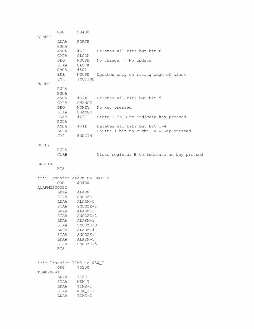
ORG $D400GINPUT LDAA PORTE PSHA ANDA #$01 Deletes all bits but bit 0 CMPA CLOCK BEQ NOUPD No change => No update STAA CLOCK CMPA #$01 BNE NOUPD Updates only on rising edge of clock JSR INCTIMENOUPD PULA PSHA ANDA #$20 Deletes all bits but bit 5 CMPA CHANGE BEQ NOKEY No key pressed STAA CHANGE LDAB #$01 Store 1 in B to indicate key pressed PULA ANDA #$1E Deletes all bits but bit 1-4 LSRA Shifts 1 bit to right. A = Key pressed JMP ENDGIN
NOKEY PULA CLRB Clear register B to indicate no key pressed
ENDGIN RTS
**** Transfer ALARM to SNOOZE ORG $D4B0ALARM2SNOOZE LDAA ALARM STAA SNOOZE LDAA ALARM+1 STAA SNOOZE+1 LDAA ALARM+2 STAA SNOOZE+2 LDAA ALARM+3 STAA SNOOZE+3 LDAA ALARM+4 STAA SNOOZE+4 LDAA ALARM+5 STAA SNOOZE+5 RTS
**** Transfer TIME to NEW_T ORG $D500TIME2NEWT LDAA TIME STAA NEW_T LDAA TIME+1 STAA NEW_T+1 LDAA TIME+2
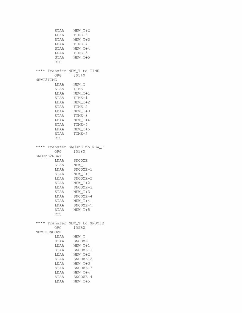
STAA NEW_T+2 LDAA TIME+3 STAA NEW_T+3 LDAA TIME+4 STAA NEW_T+4 LDAA TIME+5 STAA NEW_T+5 RTS
**** Transfer NEW_T to TIME ORG $D540NEWT2TIME LDAA NEW_T STAA TIME LDAA NEW_T+1 STAA TIME+1 LDAA NEW_T+2 STAA TIME+2 LDAA NEW_T+3 STAA TIME+3 LDAA NEW_T+4 STAA TIME+4 LDAA NEW_T+5 STAA TIME+5 RTS
**** Transfer SNOOZE to NEW_T ORG $D580SNOOZE2NEWT LDAA SNOOZE STAA NEW_T LDAA SNOOZE+1 STAA NEW_T+1 LDAA SNOOZE+2 STAA NEW_T+2 LDAA SNOOZE+3 STAA NEW_T+3 LDAA SNOOZE+4 STAA NEW_T+4 LDAA SNOOZE+5 STAA NEW_T+5 RTS
**** Transfer NEW_T to SNOOZE ORG $D5B0NEWT2SNOOZE LDAA NEW_T STAA SNOOZE LDAA NEW_T+1 STAA SNOOZE+1 LDAA NEW_T+2 STAA SNOOZE+2 LDAA NEW_T+3 STAA SNOOZE+3 LDAA NEW_T+4 STAA SNOOZE+4 LDAA NEW_T+5
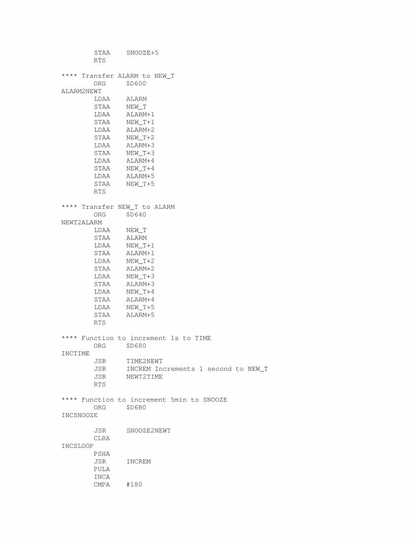
STAA SNOOZE+5 RTS
**** Transfer ALARM to NEW_T ORG $D600ALARM2NEWT LDAA ALARM STAA NEW_T LDAA ALARM+1 STAA NEW_T+1 LDAA ALARM+2 STAA NEW_T+2 LDAA ALARM+3 STAA NEW_T+3 LDAA ALARM+4 STAA NEW_T+4 LDAA ALARM+5 STAA NEW_T+5 RTS
**** Transfer NEW_T to ALARM ORG $D640NEWT2ALARM LDAA NEW_T STAA ALARM LDAA NEW_T+1 STAA ALARM+1 LDAA NEW_T+2 STAA ALARM+2 LDAA NEW_T+3 STAA ALARM+3 LDAA NEW_T+4 STAA ALARM+4 LDAA NEW_T+5 STAA ALARM+5 RTS
**** Function to increment 1s to TIME ORG $D680INCTIME JSR TIME2NEWT JSR INCREM Increments 1 second to NEW_T JSR NEWT2TIME RTS
**** Function to increment 5min to SNOOZE ORG $D6B0INCSNOOZE
JSR SNOOZE2NEWT CLRAINCSLOOP PSHA JSR INCREM PULA INCA CMPA #180
BNE INCSLOOP JSR NEWT2SNOOZE RTS
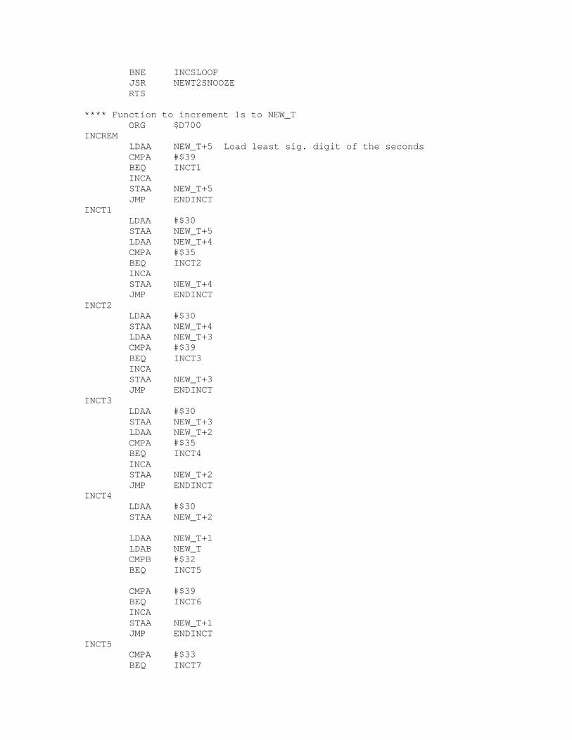
**** Function to increment 1s to NEW_T ORG $D700INCREM LDAA NEW_T+5 Load least sig. digit of the seconds CMPA #$39 BEQ INCT1 INCA STAA NEW_T+5 JMP ENDINCTINCT1 LDAA #$30 STAA NEW_T+5 LDAA NEW_T+4 CMPA #$35 BEQ INCT2 INCA STAA NEW_T+4 JMP ENDINCTINCT2 LDAA #$30 STAA NEW_T+4 LDAA NEW_T+3 CMPA #$39 BEQ INCT3 INCA STAA NEW_T+3 JMP ENDINCTINCT3 LDAA #$30 STAA NEW_T+3 LDAA NEW_T+2 CMPA #$35 BEQ INCT4 INCA STAA NEW_T+2 JMP ENDINCTINCT4 LDAA #$30 STAA NEW_T+2
LDAA NEW_T+1 LDAB NEW_T CMPB #$32 BEQ INCT5
CMPA #$39 BEQ INCT6 INCA STAA NEW_T+1 JMP ENDINCTINCT5 CMPA #$33 BEQ INCT7
INCA STAA NEW_T+1 JMP ENDINCTINCT6 LDAA #$30 STAA NEW_T+1 INCB STAB NEW_T JMP ENDINCTINCT7 LDAA #$30 STAA NEW_T+1 LDAB #$30 STAB NEW_T
ENDINCT RTS
**** Function to print time (NEW_T) on LCD (Start on ROW 2, COL 5) ORG $D800PRTIME LDAA #6 Jump to Row 2, Col 6 JSR CUR2
LDAA NEW_T JSR WRITED LDAA NEW_T+1 JSR WRITED LDAA #$3A Print ":" JSR WRITED LDAA NEW_T+2 JSR WRITED LDAA NEW_T+3 JSR WRITED LDAA #$3A Print ":" JSR WRITED LDAA NEW_T+4 JSR WRITED LDAA NEW_T+5 JSR WRITED
RTS
**** Function to edit NEW_T ORG $D900EDIT CLR EDIT_DI Starts editing digit 0 CLRB
JSR TIME2NEWT LDAA EDIT_C CMPA #0 BEQ LOOPET JSR ALARM2NEWT
LOOPET
JSR GINPUT Update time and get input. A=Key. B<>0 forkeypress PSHA PSHB LDAA EDIT_C CMPA #1 BEQ ET2 JSR TIME2NEWT
JMP ET3ET2 JSR ALARM2NEWTET3 JSR PRTIME Print time
LDAA #6 Erase everything on row 3 JSR CUR3 LDAA #$FE JSR WRITED LDAA #$FE JSR WRITED LDAA #$FE JSR WRITED LDAA #$FE JSR WRITED LDAA #$FE JSR WRITED LDAA #$FE JSR WRITED LDAA #$FE JSR WRITED LDAA #$FE JSR WRITED LDAA #6 Jumps to col correct column, row 2 LDAB EDIT_DI CMPB #4 BLO ET0 INCAET0 CMPB #2 BLO ET1 INCAET1 ADDA EDIT_DI JSR CUR3 LDAA #$5E JSR WRITED
PULB PULA CMPB #$00 BEQ LOOPET No key pressed... keep waiting
CMPA #$0A "A" pressed -> Move left BNE ET5 LDAB EDIT_DI CMPB #0
BEQ ET4 DECB STAB EDIT_DI JMP LOOPETET4 LDAB #5 STAB EDIT_DI JMP LOOPET
ET5 CMPA #$0B "B" pressed -> Move right BNE ET7 LDAB EDIT_DI CMPB #5 BEQ ET6 INCB STAB EDIT_DI JMP LOOPETET6 LDAB #0 STAB EDIT_DI JMP LOOPET
ET7 CMPA #$0F BNE ET8 JMP ENDET
ET8 LDAB EDIT_DI CMPB #0 BEQ ETD0 CMPB #1 BEQ ETD1 CMPB #2 BEQ ETD2 CMPB #3 BEQ ETD3 CMPB #4 BEQ ETD4 CMPB #5 BEQ ETD5 CLR EDIT_DI JMP LOOPET
ETD0 CMPA #$02 BHI ETD01 ADDA #$30 STAA NEW_T LDAA #1 STAA EDIT_DI JMP ETUPDATEETD01 JMP LOOPET
ETD1
LDAB NEW_T CMPB #$32 BEQ ETD11
CMPA #$09 BHI ETD12 ADDA #$30 STAA NEW_T+1 LDAA #2 STAA EDIT_DI JMP ETUPDATEETD11 CMPA #$03 BHI ETD12 ADDA #$30 STAA NEW_T+1 LDAA #2 STAA EDIT_DI JMP ETUPDATEETD12 JMP LOOPET
ETD2 CMPA #$05 BHI ETD21 ADDA #$30 STAA NEW_T+2 LDAA #3 STAA EDIT_DI JMP ETUPDATEETD21 JMP LOOPET
ETD3 CMPA #$09 BHI ETD31 ADDA #$30 STAA NEW_T+3 LDAA #4 STAA EDIT_DI JMP ETUPDATEETD31 JMP LOOPET
ETD4 CMPA #$05 BHI ETD41 ADDA #$30 STAA NEW_T+4 LDAA #5 STAA EDIT_DI JMP ETUPDATEETD41 JMP LOOPET
ETD5 CMPA #$09
BHI ETD51 ADDA #$30 STAA NEW_T+5 LDAA #0 STAA EDIT_DI JMP ETUPDATEETD51 JMP LOOPET
ETUPDATE LDAA EDIT_C CMPA #0 BNE ETUP1
JSR NEWT2TIME JMP LOOPETETUP1 JSR NEWT2ALARM JMP LOOPET
ENDET RTS
**** Function ALARM - Checks if TIME=SNOOZE**** B=0 if alarm doesn't go off ORG $DB00CK_ALARM CLRB LDAA A_STATE Check if ALARM ON/OFF CMPA #0 BEQ ENDAL If ALARM OFF, doesn't check it JSR SNOOZE2NEWT Transfers SNOOZE to NEW_T JSR CK_TIME Checks if TIME=SNOOZE CLRB CMPA #$01 BNE ENDAL Not equal... Doesn't sound alarm JSR ALARMOFF Equal... Sounds alarm LDAB #$01 Puts 1 into B to indicate alarm went offENDAL RTS
**** Function to check if TIME=NEW_T ORG $DB80CK_TIME LDAA TIME LDAB NEW_T CBA BNE ENDCK LDAA TIME+1 LDAB NEW_T+1 CBA BNE ENDCK LDAA TIME+2 LDAB NEW_T+2 CBA BNE ENDCK LDAA TIME+3
LDAB NEW_T+3 CBA BNE ENDCK LDAA TIME+4 LDAB NEW_T+4 CBA BNE ENDCK LDAA TIME+5 LDAB NEW_T+5 CBA BNE ENDCK1 LDAA #$01 JMP ENDCKENDCK1 LDAA #$00
ENDCK RTS
**** Function ALARMOFF - Sounds the alarm ORG $DC00ALARMOFF LDAA PORTA ORAA #$40 Turns on alarm STAA PORTA JSR ALSCREEN
ALLOOP JSR GINPUT Update time and get input. A=Key. B<>0 forkeypress PSHA PSHB JSR TIME2NEWT JSR PRTIME Print time PULB PULA CMPB #$00 BEQ ALLOOP No key pressed... keep waiting
CMPA #$0A BNE ALOFFB LDAA #$00 STAA A_STATE JMP ENDALOFF
ALOFFB CMPA #$0B BNE ALLOOP JSR INCSNOOZE
ENDALOFF LDAA PORTA ANDA #$BF Turns off alarm STAA PORTA
RTS
**** Function ALSCREEN - Draws screen for alarm off ORG $DD00ALSCREEN JSR CLEAR
LDAA #3 "Go to MicroPs" on col 3, row 1 JSR CUR1 LDAA #$47 JSR WRITED LDAA #$6F JSR WRITED LDAA #$FE JSR WRITED LDAA #$74 JSR WRITED LDAA #$6F JSR WRITED LDAA #$FE JSR WRITED LDAA #$4D JSR WRITED LDAA #$69 JSR WRITED LDAA #$63 JSR WRITED LDAA #$72 JSR WRITED LDAA #$6F JSR WRITED LDAA #$50 JSR WRITED LDAA #$73 JSR WRITED
LDAA #2 ">>>" JSR CUR2 LDAA #$3E JSR WRITED LDAA #$3E JSR WRITED LDAA #$3E JSR WRITED
LDAA #15 "<<<" JSR CUR2 LDAA #$3C JSR WRITED LDAA #$3C JSR WRITED LDAA #$3C JSR WRITED
LDAA #1 "A-Turn Alarm OFF" JSR CUR3 LDAA #$41 JSR WRITED LDAA #$B0
JSR WRITED LDAA #$54 JSR WRITED LDAA #$75 JSR WRITED LDAA #$72 JSR WRITED LDAA #$6E JSR WRITED LDAA #$FE JSR WRITED LDAA #$41 JSR WRITED LDAA #$6C JSR WRITED LDAA #$61 JSR WRITED LDAA #$72 JSR WRITED LDAA #$6D JSR WRITED LDAA #$FE JSR WRITED LDAA #$4F JSR WRITED LDAA #$46 JSR WRITED LDAA #$46 JSR WRITED
LDAA #1 "B-Snooze (3min)" JSR CUR4 LDAA #$42 JSR WRITED LDAA #$B0 JSR WRITED LDAA #$53 JSR WRITED LDAA #$6E JSR WRITED LDAA #$6F JSR WRITED LDAA #$6F JSR WRITED LDAA #$7A JSR WRITED LDAA #$65 JSR WRITED LDAA #$FE JSR WRITED LDAA #$28 JSR WRITED LDAA #$33 JSR WRITED LDAA #$6D JSR WRITED LDAA #$69
JSR WRITED LDAA #$6E JSR WRITED LDAA #$29 JSR WRITED
RTS
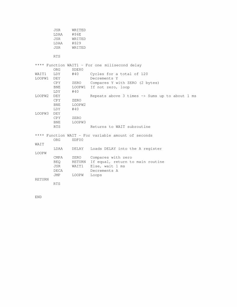
**** Function WAIT1 - For one milisecond delay ORG $DE80WAIT1 LDY #40 Cycles for a total of 120LOOPW1 DEY Decrements Y CPY ZERO Compares Y with ZERO (2 bytes) BNE LOOPW1 If not zero, loop LDY #40LOOPW2 DEY Repeats above 3 times -> Sums up to about 1 ms CPY ZERO BNE LOOPW2 LDY #40LOOPW3 DEY CPY ZERO BNE LOOPW3 RTS Returns to WAIT subroutine
**** Function WAIT - For variable amount of seconds ORG $DF00WAIT LDAA DELAY Loads DELAY into the A registerLOOPW CMPA ZERO Compares with zero BEQ RETURN If equal, return to main routine JSR WAIT1 Else, wait 1 ms DECA Decrements A JMP LOOPW LoopsRETURN RTS
END

APPENDIX C
FPGA Verilog Files

APPENDIX D
LCD Spec Sheets

Please refer to
http://www.optrex.co.jp/us/lcd_us/index.html
for the latest information on Optrex LCD information