Embed Size (px)
Citation preview
AL5809 Document number: DS36625 Rev. 5 - 2
1 of 16 www.diodes.com
December 2016 © Diodes Incorporated
AL5809
60V Two Terminal Constant Current LED Driver
PowerDI
Description
The AL5809 is a constant current linear LED driver and it provides a
cost-effective two pin solution. It has an excellent temperature
stability of 20ppm/°C and the current accuracy ±5% regulated over a
wide voltage and temperature range. The AL5809 comes in various
fixed output current versions removing the need for external current
setting resistors creating a simple solution for the linear driving of
LEDs. It supports both the high-side and low-side driving of LED
chains.
The AL5809 turns on when the voltage between IN and OUT swings
from 2.5V up to 60V enabling it drive long LED chains. The floating
ground, 60V Voltage rating between Input and Output pins designed
to withstand the high peak voltage incurred in offline applications.
The AL5809 is available in either thermally robust package
PowerDI123 or SOD-123 package.
Features
2.5V to 60V Operating Voltage Between Two Terminals
Robust Power Package Up to 1.2W for PowerDI®-123
-40°C to +125°C Temperature Range
±5% LED Current Tolerance Over-Temperature
15mA, 20mA, 25mA, 30mA, 40mA, 50mA, 60mA, 90mA,
100mA, 120mA, and 150mA Available in PowerDI123 Package
15mA, 20mA, 25mA, 30mA, 40mA and 50mA available in SOD-
123 Package, Other Current Options Available by Request
Constant Current with Low Temperature Drift and High Power
Supply Rejection Ratio
Totally Lead-Free & Fully RoHS Compliant (Notes 1 & 2)
Halogen and Antimony Free. “Green” Device (Note 3)
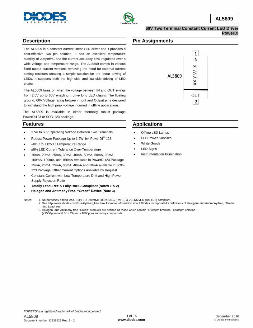
Pin Assignments
IN
OUT
XX
Y W
X
1
2
AL5809
Applications
Offline LED Lamps
LED Power Supplies
White Goods
LED Signs
Instrumentation Illumination
Notes: 1. No purposely added lead. Fully EU Directive 2002/95/EC (RoHS) & 2011/65/EU (RoHS 2) compliant. 2. See http://www.diodes.com/quality/lead_free.html for more information about Diodes Incorporated’s definitions of Halogen- and Antimony-free, "Green"
and Lead-free. 3. Halogen- and Antimony-free "Green” products are defined as those which contain <900ppm bromine, <900ppm chlorine (<1500ppm total Br + Cl) and <1000ppm antimony compounds.
POWERDI is a registered trademark of Diodes Incorporated.
AL5809 Document number: DS36625 Rev. 5 - 2
2 of 16 www.diodes.com
December 2016 © Diodes Incorporated
AL5809
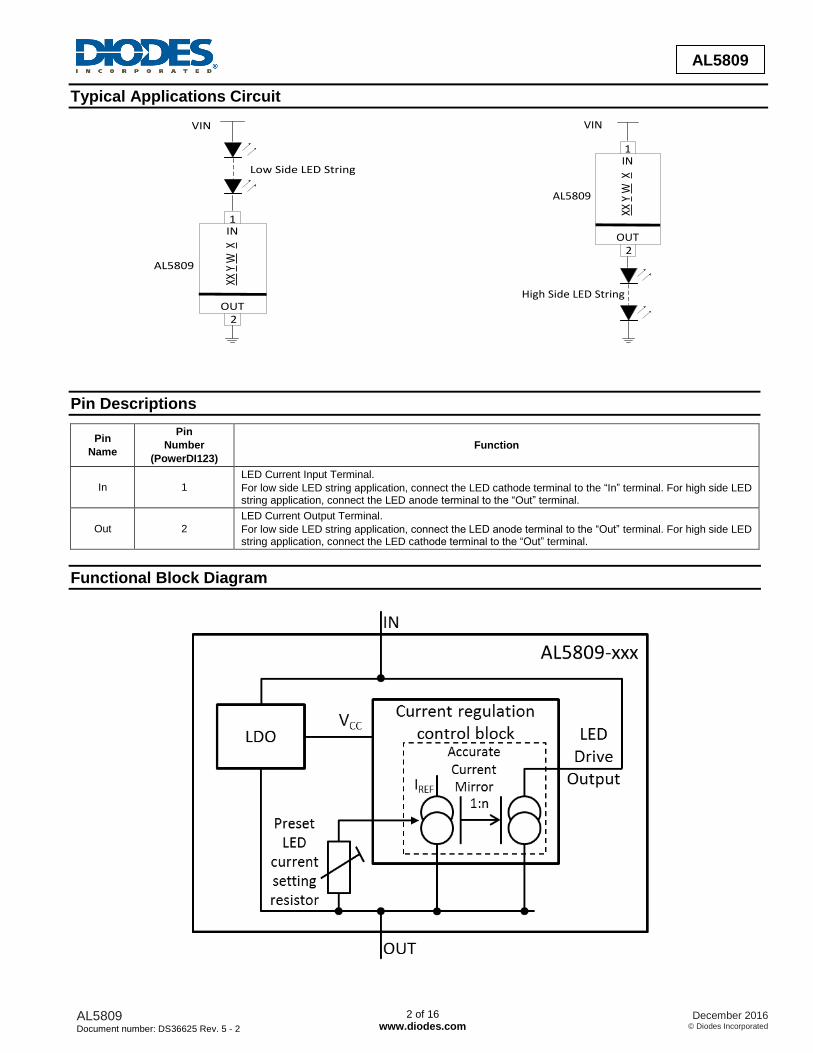
Typical Applications Circuit
VIN
Low Side LED String
IN
OUT
XX Y
W X
1
2
AL5809
VIN
High Side LED String
IN
OUT
XX Y
W X
1
2
AL5809
Pin Descriptions
Pin
Name
Pin
Number
(PowerDI123)
Function
In 1
LED Current Input Terminal.
For low side LED string application, connect the LED cathode terminal to the “In” terminal. For high side LED string application, connect the LED anode terminal to the “Out” terminal.
Out 2
LED Current Output Terminal.
For low side LED string application, connect the LED anode terminal to the “Out” terminal. For high side LED string application, connect the LED cathode terminal to the “Out” terminal.
Functional Block Diagram
AL5809 Document number: DS36625 Rev. 5 - 2
3 of 16 www.diodes.com
December 2016 © Diodes Incorporated
AL5809
Absolute Maximum Ratings
Symbol Parameters Ratings Unit
VInOut “In” Voltage Relative to “Out” Pin -0.3 to +80 V
IInOut LED Current from “In” to “Out” 180 mA
ESD HBM Human Body Model ESD Protection 4 kV
ESD MM Machine Model ESD Protection 400 V
TJ Operating Junction Temperature -40 to +175 °C
TST Storage Temperature -55 to +150 °C
Caution: Stresses greater than the 'Absolute Maximum Ratings' specified above, may cause permanent damage to the device. These are stress ratings only; functional operation of the device at these or any other conditions exceeding those indicated in this specification is not implied. Device reliability may be affected by exposure to absolute maximum rating conditions for extended periods of time. Semiconductor devices are ESD sensitive and may be damaged by exposure to ESD events. Suitable ESD precautions should be taken when handling and transporting these devices.
AL5809 Document number: DS36625 Rev. 5 - 2
4 of 16 www.diodes.com
December 2016 © Diodes Incorporated
AL5809
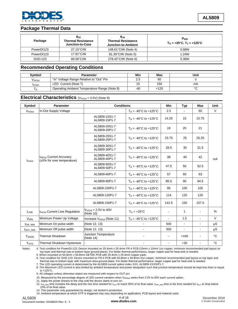
Package Thermal Data
Package
θJC
Thermal Resistance Junction-to-Case
θJA
Thermal Resistance
Junction-to-Ambient
PDIS
TA = +25°C, TJ = +125°C
PowerDI123 27.15°C/W 148.61°C/W (Note 4) 0.68W
PowerDI123 17.81°C/W 81.39°C/W (Note 5) 1.24W
SOD-123 69.56°C/W 278.42°C/W (Note 6) 0.36W
Recommended Operating Conditions
Symbol Parameter Min Max Unit
VInOut “In” Voltage Range Relative to “Out” Pin 2.5 60 V
IInOut LED Current (Note 7) 15 150 mA
TA Operating Ambient Temperature Range (Note 8) -40 +125 °C
Electrical Characteristics (VInOut = 3.5V) (Note 9)
Symbol Parameter Conditions Min Typ Max Unit
VInOut In-Out Supply Voltage - TA = -40°C to +125°C 2.5 - 60 V
IInOut IINOut Current Accuracy (±5% for over temperature)
AL5809-15S1-7 AL5809-15P1-7
TA = -40°C to +125°C 14.25 15 15.75
mA
AL5809-20S1-7 AL5809-20P1-7
TA = -40°C to +125°C 19 20 21
AL5809-25S1-7 AL5809-25P1-7
TA = -40°C to +125°C 23.75 25 26.25
AL5809-30S1-7 AL5809-30P1-7
TA = -40°C to +125°C 28.5 30 31.5
AL5809-40S1-7 AL5809-40P1-7
TA = -40°C to +125°C 38 40 42
AL5809-50S1-7 AL5809-50P1-7
TA = -40°C to +125°C 47.5 50 52.5
AL5809-60P1-7 TA = -40°C to +125°C 57 60 63
AL5809-90P1-7 TA = -40°C to +125°C 85.5 90 94.5
AL5809-100P1-7 TA = -40°C to +125°C 95 100 105
AL5809-120P1-7 TA = -40°C to +125°C 114 120 126
AL5809-150P1-7 TA = -40°C to +125°C 142.5 150 157.5
ILINE IInOut Current Line Regulation VInOut = 2.5V to 60V (Note 10)
TA = +25°C - 1 - %
VMIN Minimum Power Up Voltage Increase VInOut (Note 11) TA = -40°C to +125°C - 1.5 - V
tON_MIN Minimum On pulse width (Note 12, 13) - 500 - - µS
tOFF_MIN Minimum Off pulse width (Note 12, 13) - 500 - - µS
TSHDN Thermal Shutdown Junction Temperature (Note 14)
- - +165 - °C
THYS Thermal Shutdown Hysteresis - - - +30 - °C
Notes: 4. Test condition for PowerDI-123: Device mounted on 25.4mm x 25.4mm FR-4 PCB (10mm x 10mm 1oz copper, minimum recommended pad layout on top layer and thermal vias to bottom layer ground plane). For better thermal performance, larger copper pad for heat-sink is needed.
5. When mounted on 50.8mm x 50.8mm GETEK PCB with 25.4mm x 25.4mm copper pads. 6. Test condition for SOD-123: Device mounted on FR-4 PCB with 50.8mm x 50.8mm 2oz copper, minimum recommended pad layout on top layer and
thermal vias to bottom layer with maximum area ground plane. For better thermal performance, larger copper pad for heat-sink is needed. 7. The LED operating current is determined by the AL5809 current option index XXX, AL5809-XXXS/P1-7. 8. The Maximum LED current is also limited by ambient temperature and power dissipation such that junction temperature should be kept less than or equal
to +125°C. 9. All voltages unless otherwise stated are measured with respect to OUT pin.
10. Measured by the percentage degree of LED current variation when VInOut varies from 2.5V to 60V each current option.
11. Apply the power linearly to the chip until the device starts to turn on. 12. tON_MIN time includes the delay and the rise time needed for IOUT to reach 90% of its final value. tOFF_MIN time is the time needed for IOUT to drop below 10% of its final value. 13. This parameter only guaranteed by design, not tested in production. 14. Ambient temperature at which OTP is triggered may vary depending on application, PCB layout and material used.
AL5809 Document number: DS36625 Rev. 5 - 2
5 of 16 www.diodes.com
December 2016 © Diodes Incorporated
AL5809
Application Information
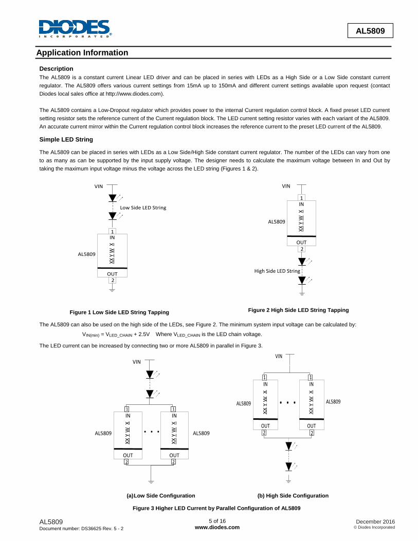
Description
The AL5809 is a constant current Linear LED driver and can be placed in series with LEDs as a High Side or a Low Side constant current
regulator. The AL5809 offers various current settings from 15mA up to 150mA and different current settings available upon request (contact
Diodes local sales office at http://www.diodes.com).
The AL5809 contains a Low-Dropout regulator which provides power to the internal Current regulation control block. A fixed preset LED current
setting resistor sets the reference current of the Current regulation block. The LED current setting resistor varies with each variant of the AL5809.
An accurate current mirror within the Current regulation control block increases the reference current to the preset LED current of the AL5809.
Simple LED String
The AL5809 can be placed in series with LEDs as a Low Side/High Side constant current regulator. The number of the LEDs can vary from one
to as many as can be supported by the input supply voltage. The designer needs to calculate the maximum voltage between In and Out by
taking the maximum input voltage minus the voltage across the LED string (Figures 1 & 2).
VIN
Low Side LED String
IN
OUT
XX Y
W X
1
2
AL5809
Figure 1 Low Side LED String Tapping
VIN
High Side LED String
IN
OUT
XX
Y W
X
1
2
AL5809
Figure 2 High Side LED String Tapping
The AL5809 can also be used on the high side of the LEDs, see Figure 2. The minimum system input voltage can be calculated by:
VIN(min) = VLED_CHAIN + 2.5V Where VLED_CHAIN is the LED chain voltage.
The LED current can be increased by connecting two or more AL5809 in parallel in Figure 3.
VIN
IN
OUT
XX
Y W
X
IN
OUT
XX
Y W
X. . .AL5809 AL5809
22
11
AL5809AL5809
VIN
IN
OUT
XX
Y W
X
IN
OUT
XX
Y W
X
. . .
1 1
22
(a) Low Side Configuration (b) High Side Configuration
Figure 3 Higher LED Current by Parallel Configuration of AL5809
AL5809 Document number: DS36625 Rev. 5 - 2
6 of 16 www.diodes.com
December 2016 © Diodes Incorporated
AL5809
Application Information (continued)
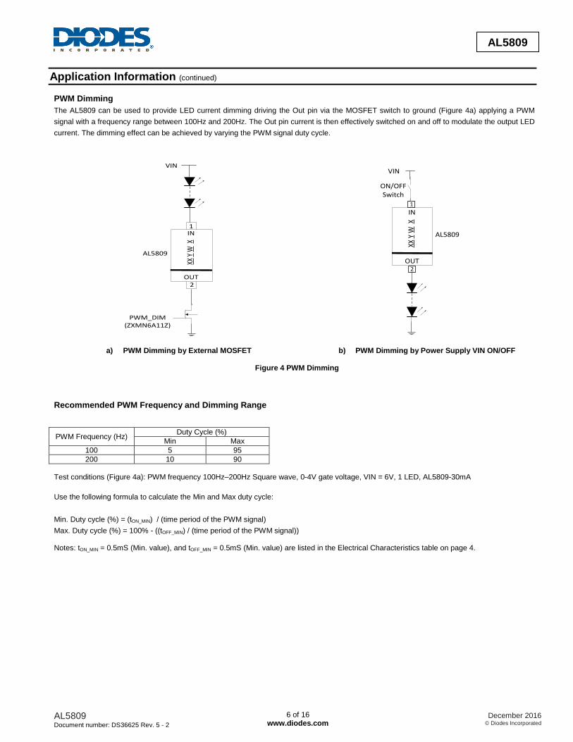
PWM Dimming
The AL5809 can be used to provide LED current dimming driving the Out pin via the MOSFET switch to ground (Figure 4a) applying a PWM
signal with a frequency range between 100Hz and 200Hz. The Out pin current is then effectively switched on and off to modulate the output LED
current. The dimming effect can be achieved by varying the PWM signal duty cycle.
VIN
PWM_DIM(ZXMN6A11Z)
IN
OUT
XX Y
W X
1
2
AL5809
a) PWM Dimming by External MOSFET
IN
OUT
XX Y
W X
VIN
ON/OFF Switch
AL5809
2
1
b) PWM Dimming by Power Supply VIN ON/OFF
Figure 4 PWM Dimming
Recommended PWM Frequency and Dimming Range
PWM Frequency (Hz) Duty Cycle (%)
Min Max
100 5 95
200 10 90
Test conditions (Figure 4a): PWM frequency 100Hz–200Hz Square wave, 0-4V gate voltage, VIN = 6V, 1 LED, AL5809-30mA
Use the following formula to calculate the Min and Max duty cycle:
Min. Duty cycle (%) = (tON_MIN) / (time period of the PWM signal)
Max. Duty cycle (%) = 100% - ((tOFF_MIN) / (time period of the PWM signal))
Notes: tON_MIN = 0.5mS (Min. value), and tOFF_MIN = 0.5mS (Min. value) are listed in the Electrical Characteristics table on page 4.
AL5809 Document number: DS36625 Rev. 5 - 2
7 of 16 www.diodes.com
December 2016 © Diodes Incorporated
AL5809
Application Information (continued)
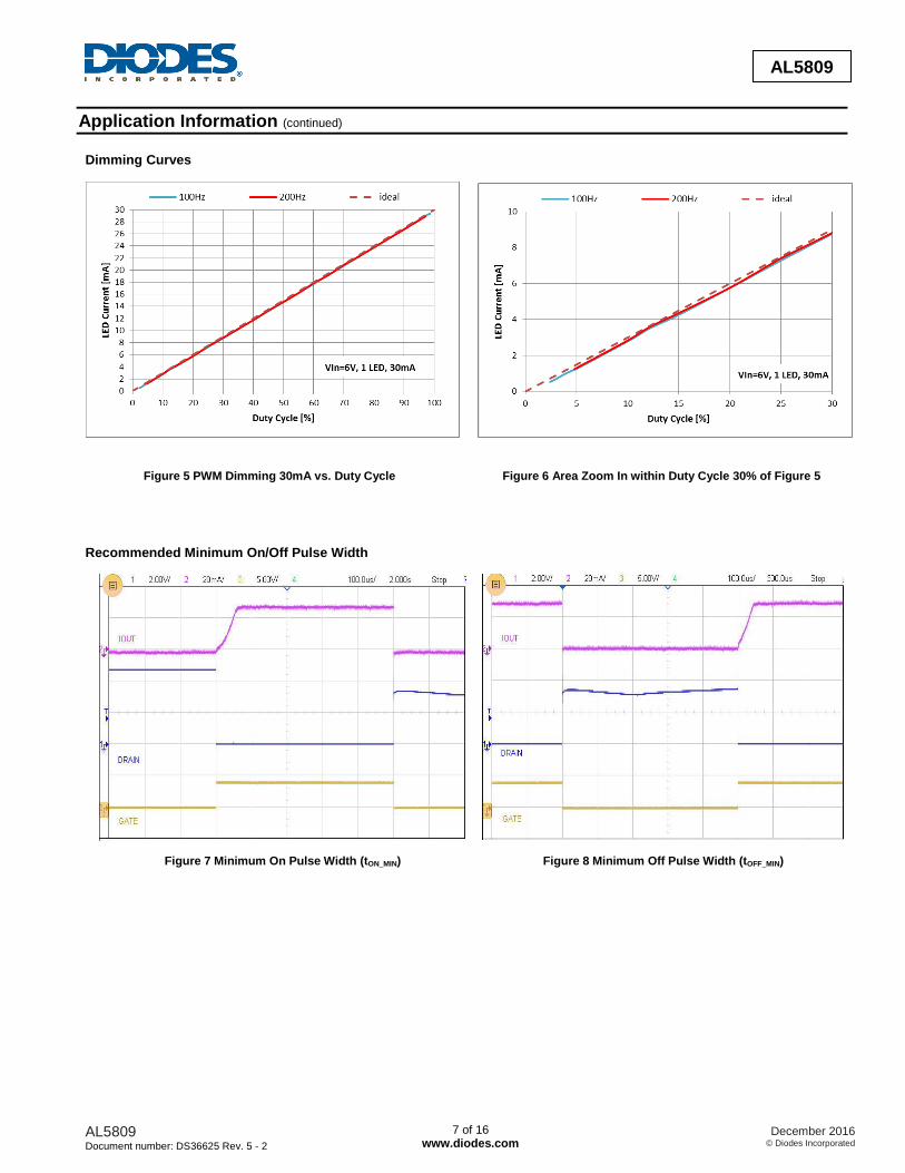
Dimming Curves
Figure 5 PWM Dimming 30mA vs. Duty Cycle
Figure 6 Area Zoom In within Duty Cycle 30% of Figure 5
Recommended Minimum On/Off Pulse Width
Figure 7 Minimum On Pulse Width (tON_MIN)
Figure 8 Minimum Off Pulse Width (tOFF_MIN)
AL5809 Document number: DS36625 Rev. 5 - 2
8 of 16 www.diodes.com
December 2016 © Diodes Incorporated
AL5809
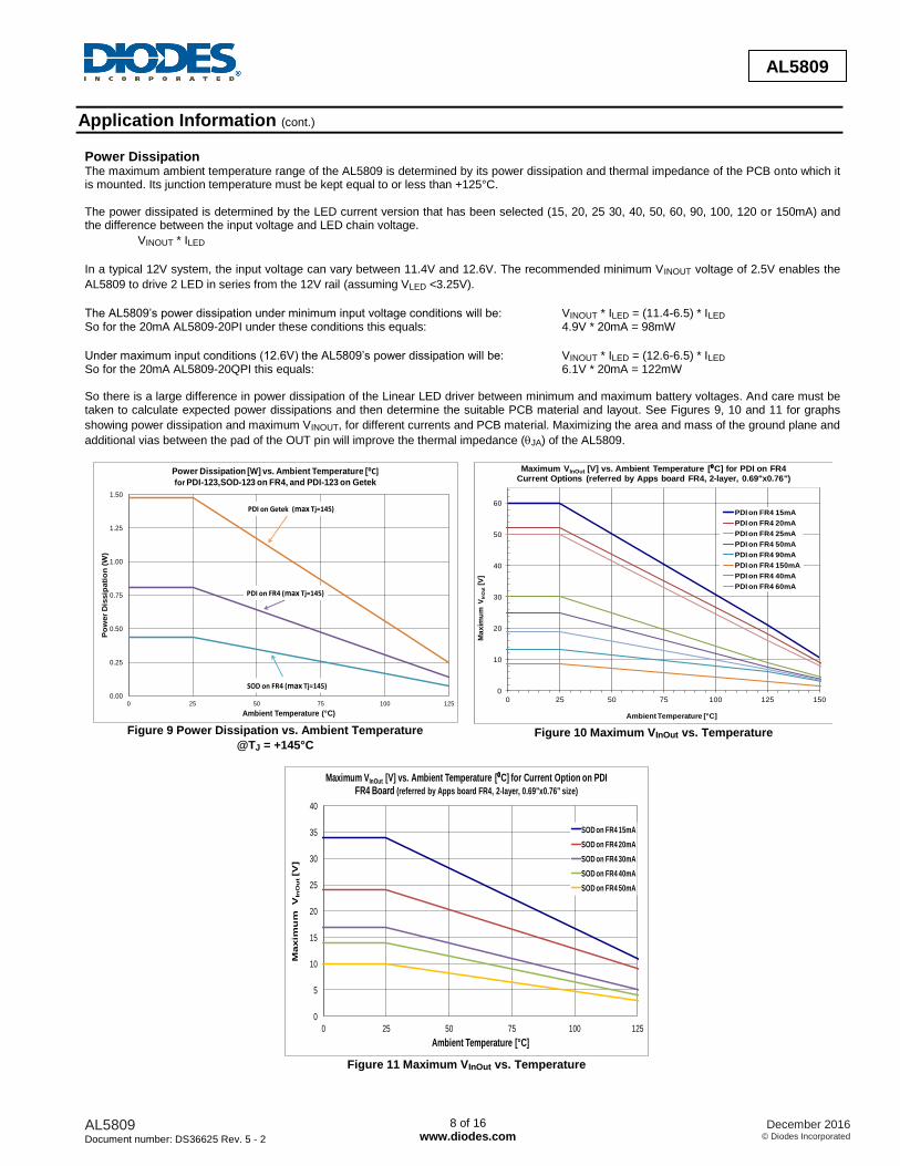
Application Information (cont.)
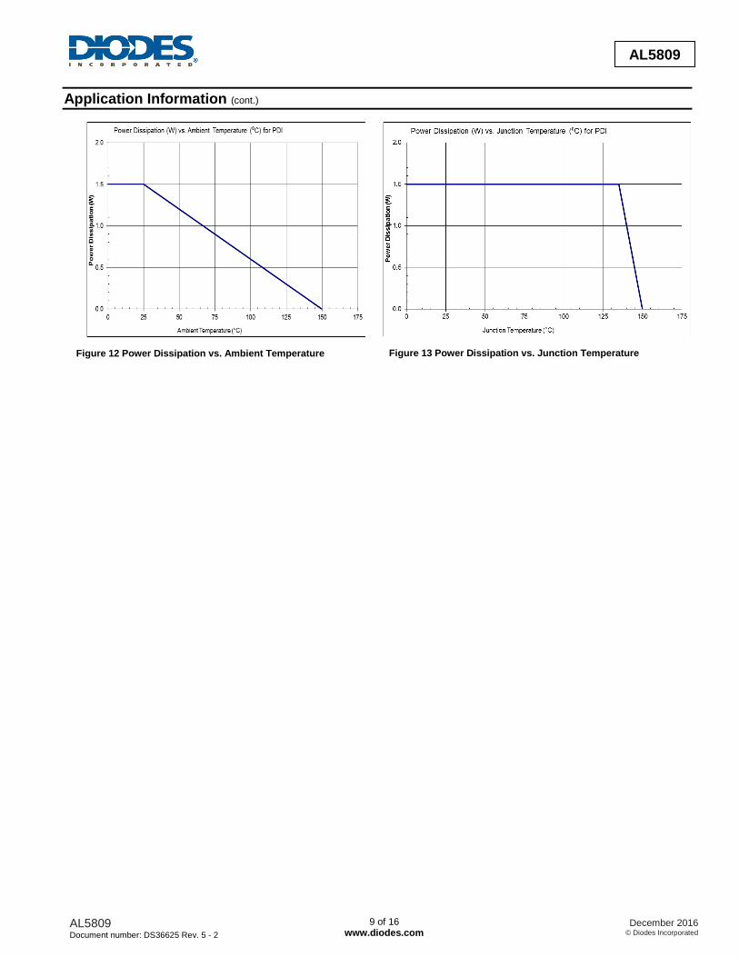
Power Dissipation The maximum ambient temperature range of the AL5809 is determined by its power dissipation and thermal impedance of the PCB onto which it is mounted. Its junction temperature must be kept equal to or less than +125°C. The power dissipated is determined by the LED current version that has been selected (15, 20, 25 30, 40, 50, 60, 90, 100, 120 or 150mA) and the difference between the input voltage and LED chain voltage.
VINOUT * ILED
In a typical 12V system, the input voltage can vary between 11.4V and 12.6V. The recommended minimum VINOUT voltage of 2.5V enables the
AL5809 to drive 2 LED in series from the 12V rail (assuming VLED <3.25V).
The AL5809’s power dissipation under minimum input voltage conditions will be: VINOUT * ILED = (11.4-6.5) * ILED So for the 20mA AL5809-20PI under these conditions this equals: 4.9V * 20mA = 98mW
Under maximum input conditions (12.6V) the AL5809’s power dissipation will be: VINOUT * ILED = (12.6-6.5) * ILED So for the 20mA AL5809-20QPI this equals: 6.1V * 20mA = 122mW So there is a large difference in power dissipation of the Linear LED driver between minimum and maximum battery voltages. And care must be taken to calculate expected power dissipations and then determine the suitable PCB material and layout. See Figures 9, 10 and 11 for graphs
showing power dissipation and maximum VINOUT, for different currents and PCB material. Maximizing the area and mass of the ground plane and
additional vias between the pad of the OUT pin will improve the thermal impedance (JA) of the AL5809.
0.00
0.25
0.50
0.75
1.00
1.25
1.50
0 25 50 75 100 125
Po
wer
Dis
sip
ati
on
(W
)
Ambient Temperature (°C)
Power Dissipation [W] vs. Ambient Temperature [⁰C] for PDI-123,SOD-123 on FR4, and PDI-123 on Getek
SOD on FR4 (max Tj=145)
PDI on Getek (max Tj=145)
PDI on FR4 (max Tj=145)
Figure 9 Power Dissipation vs. Ambient Temperature
@TJ = +145°C
0
10
20
30
40
50
60
0 25 50 75 100 125 150
Ma
xim
um
VIn
Ou
t[V
]
Ambient Temperature [°C]
Maximum VInOut [V] vs. Ambient Temperature [⁰C] for PDI on FR4
Current Options (referred by Apps board FR4, 2-layer, 0.69"x0.76")
PDI on FR4 15mA
PDI on FR4 20mA
PDI on FR4 25mA
PDI on FR4 50mA
PDI on FR4 90mA
PDI on FR4 150mA
PDI on FR4 40mA
PDI on FR4 60mA
Figure 10 Maximum VInOut vs. Temperature
0
5
10
15
20
25
30
35
40
0 25 50 75 100 125
Maxim
um
V
InO
ut [V
]
Ambient Temperature [°C]
Maximum VInOut [V] vs. Ambient Temperature [⁰C] for Current Option on PDI FR4 Board (referred by Apps board FR4, 2-layer, 0.69"x0.76" size)
SOD on FR4 15mA
SOD on FR4 20mA
SOD on FR4 30mA
SOD on FR4 40mA
SOD on FR4 50mA
Figure 11 Maximum VInOut vs. Temperature
AL5809 Document number: DS36625 Rev. 5 - 2
9 of 16 www.diodes.com
December 2016 © Diodes Incorporated
AL5809
Application Information (cont.)
Figure 12 Power Dissipation vs. Ambient Temperature
Figure 13 Power Dissipation vs. Junction Temperature
AL5809 Document number: DS36625 Rev. 5 - 2
10 of 16 www.diodes.com
December 2016 © Diodes Incorporated
AL5809
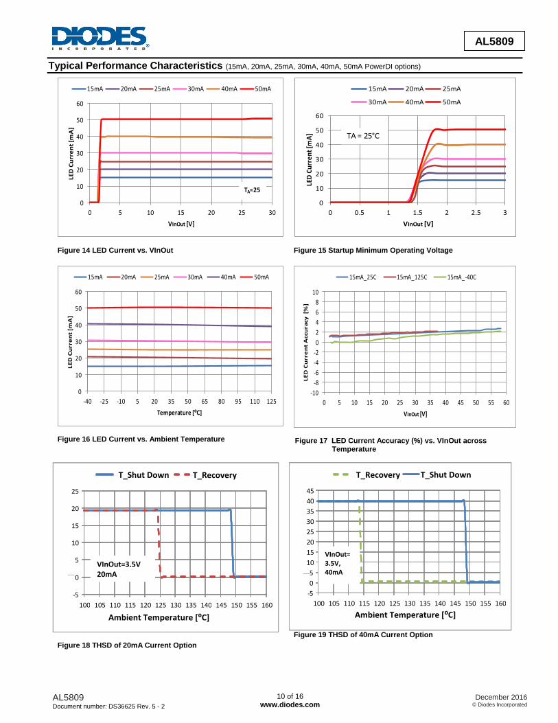
Typical Performance Characteristics (15mA, 20mA, 25mA, 30mA, 40mA, 50mA PowerDI options)
0
10
20
30
40
50
60
0 5 10 15 20 25 30
LE
D C
urr
en
t [m
A]
VInOut [V]
15mA 20mA 25mA 30mA 40mA 50mA
TA=25
Figure 14 LED Current vs. VInOut
0
10
20
30
40
50
60
0 0.5 1 1.5 2 2.5 3
LED
Cu
rre
nt
[mA
]
VInOut [V]
15mA 20mA 25mA
30mA 40mA 50mA
TA = 25°C
Figure 15 Startup Minimum Operating Voltage
0
10
20
30
40
50
60
-40 -25 -10 5 20 35 50 65 80 95 110 125
LE
D C
urr
en
t [m
A]
Temperature [⁰C]
15mA 20mA 25mA 30mA 40mA 50mA
Figure 16 LED Current vs. Ambient Temperature
-10
-8
-6
-4
-2
0
2
4
6
8
10
0 5 10 15 20 25 30 35 40 45 50 55 60
LE
D C
urr
en
t A
ccu
racy
[%
]
VInOut [V]
15mA_25C 15mA_125C 15mA_-40C
Figure 17 LED Current Accuracy (%) vs. VInOut across Temperature
Figure 18 THSD of 20mA Current Option
Figure 19 THSD of 40mA Current Option
- 5
0
5
10
15
20
25
100 105 110 115 120 125 130 135 140 145 150 155 160
LED Current [mA]
Ambient Temperature [⁰C]
T_Shut Down T_Recovery
VInOut=3.5V 20mA
- 5 0 5
10 15 20 25 30 35 40 45
100 105 110 115 120 125 130 135 140 145 150 155 160
LED Current [mA]
Ambient Temperature [⁰C]
T_Recovery T_Shut Down
VInOut=3.5V, 40mA
AL5809 Document number: DS36625 Rev. 5 - 2
11 of 16 www.diodes.com
December 2016 © Diodes Incorporated
AL5809
Typical Performance Characteristics (continued) (60mA, 90mA, 150mA PowerDI options)
Figure 20 LED Current vs. VInOut
0
20
40
60
80
100
120
140
160
0 0.5 1 1.5 2 2.5 3
LE
D C
urr
en
t [m
A]
VInOut [V]
60mA 90mA 150mA
TA=25⁰C
Figure 21 Startup Minimum Operating Voltage
VInOut=3.5
Temperature[⁰C]
Figure 22 LED Current across Temperature Figure 23 LED Current Accuracy (%) vs. VInOut across Temperature
Figure 24 THSD of 60mA Current Option
Figure 25 THSD of 150mA Current Option
- 20 0
20 40 60 80
100 120 140 160
100 110 120 130 140 150 160
LED Current [mA]
Temperature [⁰C]
T_Recovery T_Shut Down
VInOut=3.5V 150mA
- 10 0
10 20 30 40 50 60 70
100 110 120 130 140 150 160
LED Current [mA]
Ambient Tempature [⁰C]
T_Shut Down T_Recovery
VInOut=3.5V 60mA
0
20
40
60
80
100
120
140
160
0 5 10 15 20 25 30
LED Current [mA]
V InOut [V]
60mA 90mA 150mA
TA=25⁰CC
AL5809 Document number: DS36625 Rev. 5 - 2
12 of 16 www.diodes.com
December 2016 © Diodes Incorporated
AL5809
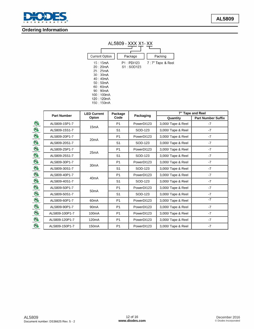
Ordering Information
Part Number
LED Current Opion
Package Code
Packaging 7” Tape and Reel
Quantity Part Number Suffix
AL5809-15P1-7 15mA
P1 PowerDI123 3,000/ Tape & Reel -7
AL5809-15S1-7 S1 SOD-123 3,000/ Tape & Reel -7
AL5809-20P1-7 20mA
P1 PowerDI123 3,000/ Tape & Reel -7
AL5809-20S1-7 S1 SOD-123 3,000/ Tape & Reel -7
AL5809-25P1-7 25mA
P1 PowerDI123 3,000/ Tape & Reel -7
AL5809-25S1-7 S1 SOD-123 3,000/ Tape & Reel -7
AL5809-30P1-7 30mA
P1 PowerDI123 3,000/ Tape & Reel -7
AL5809-30S1-7 S1 SOD-123 3,000/ Tape & Reel -7
AL5809-40P1-7 40mA
P1 PowerDI123 3,000/ Tape & Reel -7
AL5809-40S1-7 S1 SOD-123 3,000/ Tape & Reel -7
AL5809-50P1-7 50mA
P1 PowerDI123 3,000/ Tape & Reel -7
AL5809-50S1-7 S1 SOD-123 3,000/ Tape & Reel -7
AL5809-60P1-7 60mA P1 PowerDI123 3,000/ Tape & Reel -7
AL5809-90P1-7 90mA P1 PowerDI123 3,000/ Tape & Reel -7
AL5809-100P1-7 100mA P1 PowerDI123 3,000/ Tape & Reel -7
AL5809-120P1-7 120mA P1 PowerDI123 3,000/ Tape & Reel -7
AL5809-150P1-7 150mA P1 PowerDI123 3,000/ Tape & Reel -7
AL5809 Document number: DS36625 Rev. 5 - 2
13 of 16 www.diodes.com
December 2016 © Diodes Incorporated
AL5809
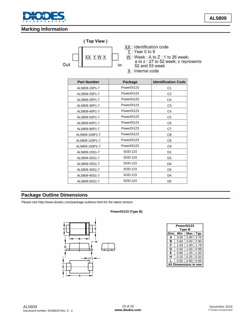
Marking Information
Part Number Package Identification Code
AL5809-15P1-7 PowerDI123 C1
AL5809-20P1-7 PowerDI123 C2
AL5809-25P1-7 PowerDI123 CA
AL5809-30P1-7 PowerDI123 C3
AL5809-40P1-7 PowerDI123 C4
AL5809-50P1-7 PowerDI123 C5
AL5809-60P1-7 PowerDI123 C6
AL5809-90P1-7 PowerDI123 C7
AL5809-100P1-7 PowerDI123 CB
AL5809-120P1-7 PowerDI123 C8
AL5809-150P1-7 PowerDI123 C9
AL5809-15S1-7 SOD-123 D1
AL5809-20S1-7 SOD-123 D2
AL5809-25S1-7 SOD-123 DA
AL5809-30S1-7 SOD-123 D3
AL5809-40S1-7 SOD-123 D4
AL5809-50S1-7 SOD-123 D5
Package Outline Dimensions
Please see http://www.diodes.com/package-outlines.html for the latest version.
PowerDI123 (Type B)
PowerDI123 Type B
Dim Min Max Typ
A 3.50 3.90 3.70
B 2.60 3.00 2.80
C 1.63 1.93 1.78
D 0.93 1.00 0.98
E 0.85 1.25 1.00
H 0.15 0.25 0.20
L 0.50 0.80 0.65
All Dimensions in mm
L
EC
A
B
D
H
E
AL5809 Document number: DS36625 Rev. 5 - 2
14 of 16 www.diodes.com
December 2016 © Diodes Incorporated
AL5809
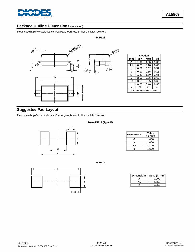
Package Outline Dimensions (continued)
Please see http://www.diodes.com/package-outlines.html for the latest version.
SOD123
c
He
E
b D
All 7
°All R
0.100
a
L
A
A1
All R0.100
All 7°
SOD123
Dim Min Max Typ
A 1.00 1.35 1.05
A1 0.00 0.10 0.05
b 0.52 0.62 0.57
c 0.10 0.15 0.11
D 1.40 1.70 1.55
E 2.55 2.85 2.65
He 3.55 3.85 3.65
L 0.25 0.40 0.30
a 0º 8º --
All Dimensions in mm
Suggested Pad Layout
Please see http://www.diodes.com/package-outlines.html for the latest version.
PowerDI123 (Type B)
X
Y
X1
G
Dimensions Value
(in mm)
G 2.000
X 1.050
X1 4.100
Y 1.500
SOD123
Y
X
X1
Dimensions Value (in mm)
X 0.900
X1 4.050
Y 0.950
AL5809 Document number: DS36625 Rev. 5 - 2
15 of 16 www.diodes.com
December 2016 © Diodes Incorporated
AL5809
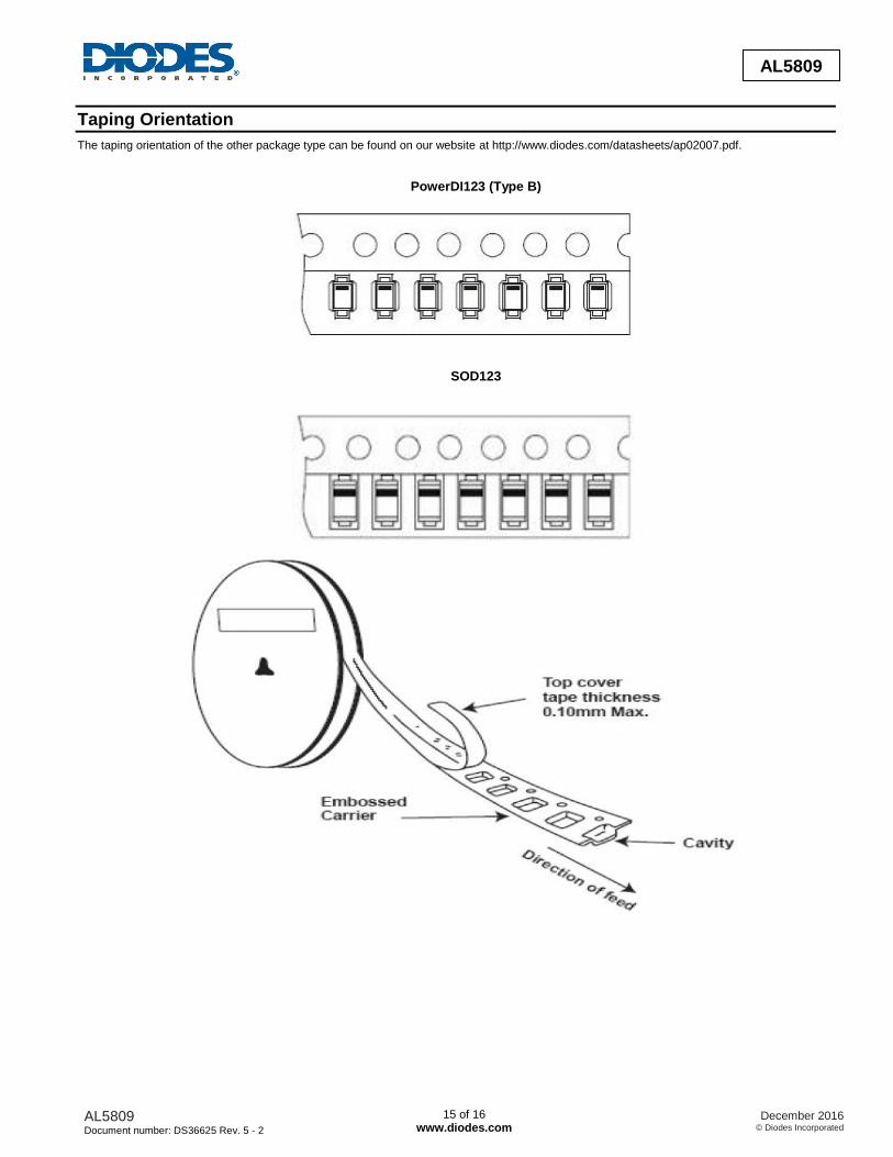
Taping Orientation
The taping orientation of the other package type can be found on our website at http://www.diodes.com/datasheets/ap02007.pdf.
PowerDI123 (Type B)
SOD123
AL5809 Document number: DS36625 Rev. 5 - 2
16 of 16 www.diodes.com
December 2016 © Diodes Incorporated
AL5809
IMPORTANT NOTICE DIODES INCORPORATED MAKES NO WARRANTY OF ANY KIND, EXPRESS OR IMPLIED, WITH REGARDS TO THIS DOCUMENT, INCLUDING, BUT NOT LIMITED TO, THE IMPLIED WARRANTIES OF MERCHANTABILITY AND FITNESS FOR A PARTICULAR PURPOSE (AND THEIR EQUIVALENTS UNDER THE LAWS OF ANY JURISDICTION). Diodes Incorporated and its subsidiaries reserve the right to make modifications, enhancements, improvements, corrections or other changes without further notice to this document and any product described herein. Diodes Incorporated does not assume any liability arising out of the application or use of this document or any product described herein; neither does Diodes Incorporated convey any license under its patent or trademark rights, nor the rights of others. Any Customer or user of this document or products described herein in such applications shall assume all risks of such use and will agree to hold Diodes Incorporated and all the companies whose products are represented on Diodes Incorporated website, harmless against all damages. Diodes Incorporated does not warrant or accept any liability whatsoever in respect of any products purchased through unauthorized sales channel. Should Customers purchase or use Diodes Incorporated products for any unintended or unauthorized application, Customers shall indemnify and hold Diodes Incorporated and its representatives harmless against all claims, damages, expenses, and attorney fees arising out of, directly or indirectly, any claim of personal injury or death associated with such unintended or unauthorized application. Products described herein may be covered by one or more United States, international or foreign patents pending. Product names and markings noted herein may also be covered by one or more United States, international or foreign trademarks. This document is written in English but may be translated into multiple languages for reference. Only the English version of this document is the final and determinative format released by Diodes Incorporated.
LIFE SUPPORT Diodes Incorporated products are specifically not authorized for use as critical components in life support devices or systems without the express written approval of the Chief Executive Officer of Diodes Incorporated. As used herein: A. Life support devices or systems are devices or systems which: 1. are intended to implant into the body, or
2. support or sustain life and whose failure to perform when properly used in accordance with instructions for use provided in the labeling can be reasonably expected to result in significant injury to the user.
B. A critical component is any component in a life support device or system whose failure to perform can be reasonably expected to cause the failure of the life support device or to affect its safety or effectiveness. Customers represent that they have all necessary expertise in the safety and regulatory ramifications of their life support devices or systems, and acknowledge and agree that they are solely responsible for all legal, regulatory and safety-related requirements concerning their products and any use of Diodes Incorporated products in such safety-critical, life support devices or systems, notwithstanding any devices- or systems-related information or support that may be provided by Diodes Incorporated. Further, Customers must fully indemnify Diodes Incorporated and its representatives against any damages arising out of the use of Diodes Incorporated products in such safety-critical, life support devices or systems. Copyright © 2016, Diodes Incorporated www.diodes.com