Embed Size (px)
Citation preview
AL5802LP Document number: DS37549 Rev. 4 - 2
1 of 10 www.diodes.com
March 2016 © Diodes Incorporated
AD
VA
NC
E IN
FO
RM
AT
IO
N
NE
W P
RO
DU
CT
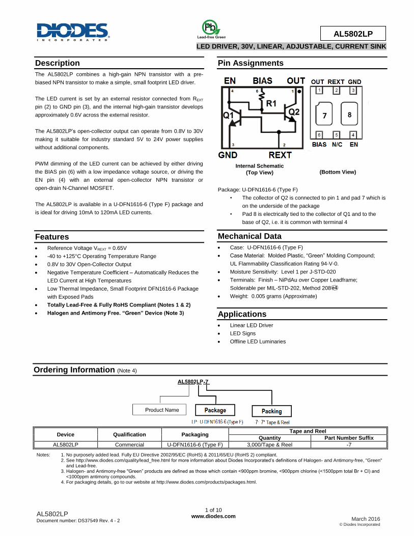
AL5802LP
LED DRIVER, 30V, LINEAR, ADJUSTABLE, CURRENT SINK
Description
The AL5802LP combines a high-gain NPN transistor with a pre-
biased NPN transistor to make a simple, small footprint LED driver.
The LED current is set by an external resistor connected from REXT
pin (2) to GND pin (3), and the internal high-gain transistor develops
approximately 0.6V across the external resistor.
The AL5802LP’s open-collector output can operate from 0.8V to 30V
making it suitable for industry standard 5V to 24V power supplies
without additional components.
PWM dimming of the LED current can be achieved by either driving
the BIAS pin (6) with a low impedance voltage source, or driving the
EN pin (4) with an external open-collector NPN transistor or
open-drain N-Channel MOSFET.
The AL5802LP is available in a U-DFN1616-6 (Type F) package and
is ideal for driving 10mA to 120mA LED currents.
Features
Reference Voltage VREXT = 0.65V
-40 to +125°C Operating Temperature Range
0.8V to 30V Open-Collector Output
Negative Temperature Coefficient – Automatically Reduces the
LED Current at High Temperatures
Low Thermal Impedance, Small Footprint DFN1616-6 Package
with Exposed Pads
Totally Lead-Free & Fully RoHS Compliant (Notes 1 & 2)
Halogen and Antimony Free. “Green” Device (Note 3)
Pin Assignments
Package: U-DFN1616-6 (Type F)
• The collector of Q2 is connected to pin 1 and pad 7 which is
on the underside of the package
• Pad 8 is electrically tied to the collector of Q1 and to the
base of Q2, i.e. it is common with terminal 4
Mechanical Data
Case: U-DFN1616-6 (Type F)
Case Material: Molded Plastic, “Green” Molding Compound;
UL Flammability Classification Rating 94-V-0.
Moisture Sensitivity: Level 1 per J-STD-020
Terminals: Finish – NiPdAu over Copper Leadframe;
Solderable per MIL-STD-202, Method 208
Weight: 0.005 grams (Approximate)
Applications
Linear LED Driver
LED Signs
Offline LED Luminaries
Ordering Information (Note 4)
Device Qualification Packaging Tape and Reel
Quantity Part Number Suffix
AL5802LP Commercial U-DFN1616-6 (Type F) 3,000/Tape & Reel -7
Notes: 1. No purposely added lead. Fully EU Directive 2002/95/EC (RoHS) & 2011/65/EU (RoHS 2) compliant. 2. See http://www.diodes.com/quality/lead_free.html for more information about Diodes Incorporated’s definitions of Halogen- and Antimony-free, "Green" and Lead-free. 3. Halogen- and Antimony-free "Green” products are defined as those which contain <900ppm bromine, <900ppm chlorine (<1500ppm total Br + Cl) and <1000ppm antimony compounds. 4. For packaging details, go to our website at http://www.diodes.com/products/packages.html.
Internal Schematic
(Top View) (Bottom View)
e4
AL5802LP Document number: DS37549 Rev. 4 - 2
2 of 10 www.diodes.com
March 2016 © Diodes Incorporated
AD
VA
NC
E IN
FO
RM
AT
IO
N
NE
W P
RO
DU
CT
AL5802LP
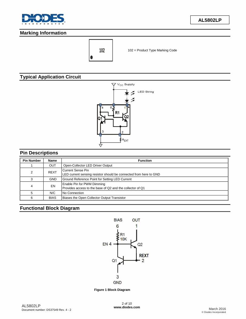
Marking Information
Typical Application Circuit
Pin Descriptions
Pin Number Name Function
1 OUT Open-Collector LED Driver Output
2 REXT Current Sense Pin
LED current sensing resistor should be connected from here to GND
3 GND Ground Reference Point for Setting LED Current
4 EN Enable Pin for PWM Dimming
Provides access to the base of Q2 and the collector of Q1
5 N/C No Connection
6 BIAS Biases the Open Collector Output Transistor
Functional Block Diagram
Figure 1 Block Diagram
102 102 = Product Type Marking Code
AL5802LP Document number: DS37549 Rev. 4 - 2
3 of 10 www.diodes.com
March 2016 © Diodes Incorporated
AD
VA
NC
E IN
FO
RM
AT
IO
N
NE
W P
RO
DU
CT
AL5802LP
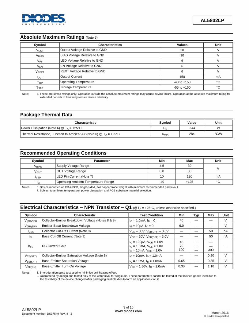
Absolute Maximum Ratings (Note 5)
Symbol Characteristics Values Unit
VOUT Output Voltage Relative to GND 30 V
VBIAS BIAS Voltage Relative to GND 30 V
VFB LED Voltage Relative to GND 6 V
VEN EN Voltage Relative to GND 6 V
VREXT REXT Voltage Relative to GND 6 V
IOUT Output Current 150 mA
TOP Operating Temperature -40 to +150 °C
TSTG Storage Temperature -55 to +150 °C
Note: 5. These are stress ratings only. Operation outside the absolute maximum ratings may cause device failure. Operation at the absolute maximum rating for extended periods of time may reduce device reliability.
Package Thermal Data
Characteristic Symbol Value Unit
Power Dissipation (Note 6) @ TA = +25°C PD 0.44 W
Thermal Resistance, Junction to Ambient Air (Note 6) @ TA = +25°C RθJA 284 °C/W
Recommended Operating Conditions
Symbol Parameter Min Max Unit
VBIAS Supply Voltage Range 4.5 30 V
VOUT OUT Voltage Range 0.8 30
ILED LED Pin Current (Note 7) 10 120 mA
TA Operating Ambient Temperature Range -40 +125 °C
Notes: 6. Device mounted on FR-4 PCB, single-sided, 2oz copper trace weight with minimum recommended pad layout.
7. Subject to ambient temperature, power dissipation and PCB substrate material selection.
Electrical Characteristics – NPN Transistor – Q1 (@TA = +25°C, unless otherwise specified.)
Symbol Characteristic Test Condition Min Typ Max Unit
V(BR)CEO Collector-Emitter Breakdown Voltage (Notes 8 & 9) IC = 1.0mA, IB = 0 40 — — V
V(BR)EBO Emitter-Base Breakdown Voltage IE = 10µA, IC = 0 6.0 — — V
ICEX Collector Cut-Off Current (Note 9) VCE = 30V, VEB(OFF) = 3.0V — — 50 nA
IBL Base Cut-Off Current (Note 9) VCE = 30V, VEB(OFF) = 3.0V — — 50 nA
hFE DC Current Gain
IC = 100µA, VCE = 1.0V
IC = 1.0mA, VCE = 1.0V
IC = 10mA, VCE = 1.0V
40 70 100
—
—
—
—
— 300
—
VCE(SAT) Collector-Emitter Saturation Voltage (Note 8) IC = 10mA, IB = 1.0mA — — 0.20 V
VBE(SAT) Base-Emitter Saturation Voltage IC = 10mA, IB = 1.0mA 0.65 — 0.85 V
VBE(ON) Base-Emitter Turn-On Voltage VCE = 1.50V, IC = 2.0mA 0.30 — 1.10 V
Notes: 8. Short duration pulse test used to minimize self-heating effect. 9. Guaranteed by design and tested only at the wafer level for single die. These parameters cannot be tested at the finished goods level due to the testability of the device changed after packaging multiple dies to form an application circuit.
AL5802LP Document number: DS37549 Rev. 4 - 2
4 of 10 www.diodes.com
March 2016 © Diodes Incorporated
AD
VA
NC
E IN
FO
RM
AT
IO
N
NE
W P
RO
DU
CT
AL5802LP
Electrical Characteristics – NPN Pre-biased Transistor – Q2 (@TA = +25°C, unless otherwise specified.)
Symbol Characteristic Test Condition Min Typ Max Unit
V(BR)CBO Collector-Base Breakdown Voltage IC = 50μA, IE = 0 30 — — V
V(BR)CEO Collector-Emitter Breakdown Voltage (Note 8) IC = 1mA, IB = 0 30 — — V
V(BR)EBO Emitter-Base Breakdown Voltage (Note 9) IE = 50μA, IC = 0 5.0 — — V
ICBO Collector Cut-Off Current VCB = 30V, IE = 0 — — 0.5 µA
IEBO Emitter Cut-Off Current (Note 9) VEB = 4V, IC = 0 — — 0.5 µA
VCE(SAT) Collector-Emitter Saturation Voltage (Note 8) IC = 10mA, IB = 1mA — — 0.3 V
VBE(ON) Base-Emitter Turn-On Voltage VCE = 5.0V, IC = 2.0mA 0.30 — 1.10 V
hFE DC Current Gain (Note 8) VCE = 5V, IC = 150mA 100 — — —
R1 Input Resistance — 7 10 13 kΩ
Notes: 8. Short duration pulse test used to minimize self-heating effect. 9. Guaranteed by design and tested only at the wafer level for single die. These parameters cannot be tested at the finished goods level due to the testability of the device changed after packaging multiple dies to form an application circuit.
Thermal Characteristics
Typical Performance Characteristics
VOUT (V)
Figure 3 Output Current vs. VOUT
Figure 4 Output Current vs. Rext Rext ( )Ω
0
50
100
1 10 100
I (
mA
)ou
t
Vout = 1.4V
Vout = 5.4V
Vbias = 24V
AL5802LP Document number: DS37549 Rev. 4 - 2
5 of 10 www.diodes.com
March 2016 © Diodes Incorporated
AD
VA
NC
E IN
FO
RM
AT
IO
N
NE
W P
RO
DU
CT
AL5802LP
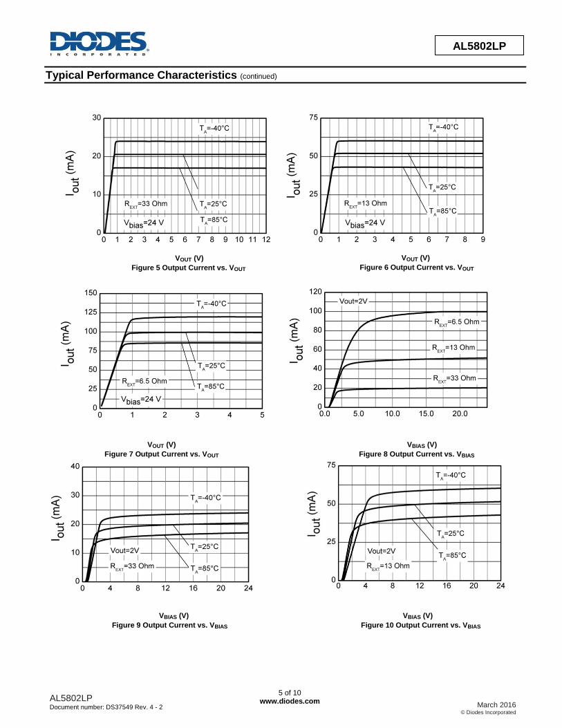
Typical Performance Characteristics (continued)
VOUT (V)
Figure 5 Output Current vs. VOUT
VOUT (V)
Figure 6 Output Current vs. VOUT
VOUT (V)
Figure 7 Output Current vs. VOUT
VBIAS (V)
Figure 8 Output Current vs. VBIAS
VBIAS (V)
Figure 9 Output Current vs. VBIAS
VBIAS (V)
Figure 10 Output Current vs. VBIAS
AL5802LP Document number: DS37549 Rev. 4 - 2
6 of 10 www.diodes.com
March 2016 © Diodes Incorporated
AD
VA
NC
E IN
FO
RM
AT
IO
N
NE
W P
RO
DU
CT
AL5802LP
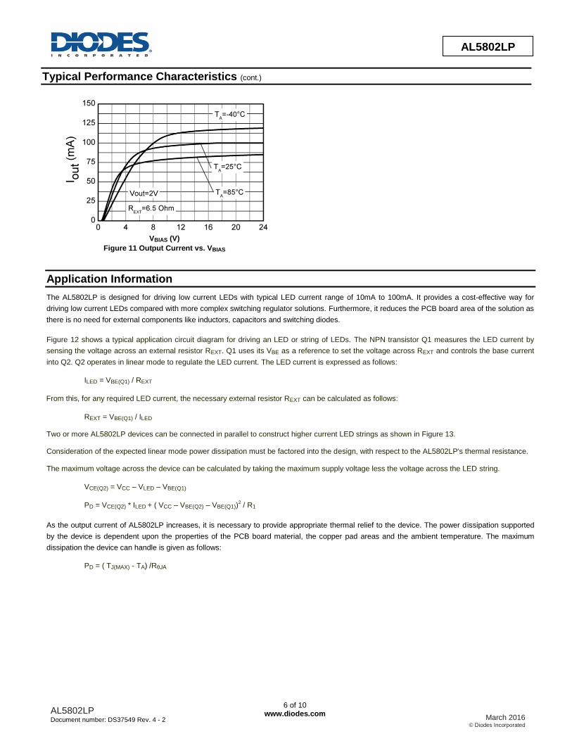
Typical Performance Characteristics (cont.)
VBIAS (V)
Figure 11 Output Current vs. VBIAS
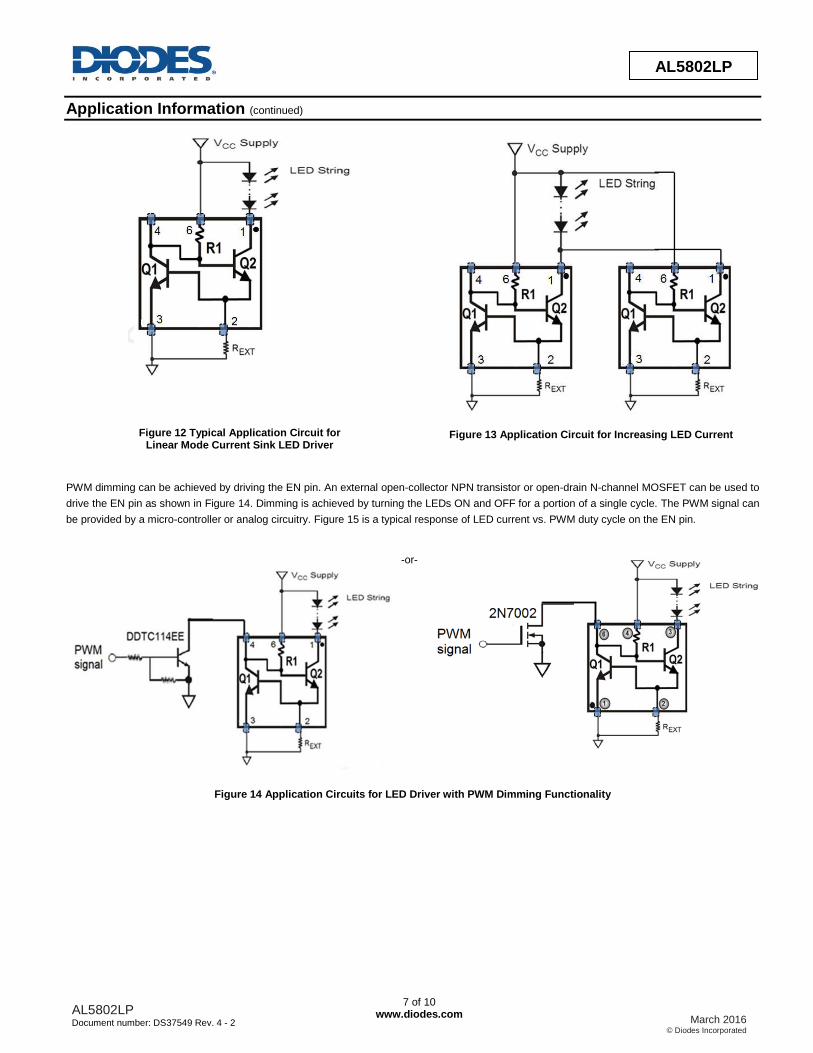
Application Information
The AL5802LP is designed for driving low current LEDs with typical LED current range of 10mA to 100mA. It provides a cost-effective way for
driving low current LEDs compared with more complex switching regulator solutions. Furthermore, it reduces the PCB board area of the solution as
there is no need for external components like inductors, capacitors and switching diodes.
Figure 12 shows a typical application circuit diagram for driving an LED or string of LEDs. The NPN transistor Q1 measures the LED current by
sensing the voltage across an external resistor REXT. Q1 uses its VBE as a reference to set the voltage across REXT and controls the base current
into Q2. Q2 operates in linear mode to regulate the LED current. The LED current is expressed as follows:
ILED = VBE(Q1) / REXT
From this, for any required LED current, the necessary external resistor REXT can be calculated as follows:
REXT = VBE(Q1) / ILED Two or more AL5802LP devices can be connected in parallel to construct higher current LED strings as shown in Figure 13. Consideration of the expected linear mode power dissipation must be factored into the design, with respect to the AL5802LP's thermal resistance. The maximum voltage across the device can be calculated by taking the maximum supply voltage less the voltage across the LED string.
VCE(Q2) = VCC – VLED – VBE(Q1)
PD = VCE(Q2) * ILED + ( VCC – VBE(Q2) – VBE(Q1))2 / R1
As the output current of AL5802LP increases, it is necessary to provide appropriate thermal relief to the device. The power dissipation supported
by the device is dependent upon the properties of the PCB board material, the copper pad areas and the ambient temperature. The maximum
dissipation the device can handle is given as follows:
PD = ( TJ(MAX) - TA) /RθJA
AL5802LP Document number: DS37549 Rev. 4 - 2
7 of 10 www.diodes.com
March 2016 © Diodes Incorporated
AD
VA
NC
E IN
FO
RM
AT
IO
N
NE
W P
RO
DU
CT
AL5802LP
Application Information (continued)
Figure 12 Typical Application Circuit for Linear Mode Current Sink LED Driver
Figure 13 Application Circuit for Increasing LED Current
PWM dimming can be achieved by driving the EN pin. An external open-collector NPN transistor or open-drain N-channel MOSFET can be used to
drive the EN pin as shown in Figure 14. Dimming is achieved by turning the LEDs ON and OFF for a portion of a single cycle. The PWM signal can
be provided by a micro-controller or analog circuitry. Figure 15 is a typical response of LED current vs. PWM duty cycle on the EN pin.
-or-
Figure 14 Application Circuits for LED Driver with PWM Dimming Functionality
AL5802LP Document number: DS37549 Rev. 4 - 2
8 of 10 www.diodes.com
March 2016 © Diodes Incorporated
AD
VA
NC
E IN
FO
RM
AT
IO
N
NE
W P
RO
DU
CT
AL5802LP
SBR is a registered trademark of Diodes Incorporated
Application Information (cont.)
Figure 15 Typical LED Current Response vs. PWM Duty Cycle for
REXT = 13Ω at 400Hz PWM Frequency
To remove the potential of incorrect connection of the power supply damaging the lamp’s LEDs, many systems use some form of reverse polarity
protection.
One solution for reverse input polarity protection is to simply use a diode with a low VF in-line with the driver/LED combination. The low VF of the
series connected diode increases the available voltage to the LED stack and dissipates less power. A circuit example is presented in Figure 16
using Diodes Inc. SBR® (Super Barrier Rectifier) technology. An SDM10U45LP (0.1A/45V) is shown, providing exceptionally low VF for its package
size of 1mm x 0.6mm, equivalent to an 0402 chip style package. Other reverse voltage ratings are also available on Diodes Inc.’s website such as
the SBR02U100LP (0.2A/100V) or SBR0220LP (0.2A/20V). Automotive applications commonly use this method for reverse battery protection. A second approach, shown in Figure 17, improves upon the method shown in Figure 16. Whereas the method in Figure 16 protects the light engine, it will not function until the problem has been diagnosed and corrected.
The method shown in Figure 17 not only provides reverse polarity protection, it also corrects the reversed polarity, allowing the light engine to
function.
The BAS40BRW incorporates four low VF, Schottky diodes into a single package and allows more voltage available for the LED stack and
dissipates less power than standard rectifier bridges.
Figure 16 Application Circuit for LED Driver
with Reverse Polarity Protection
Figure 17 Application Circuit for LED Driver with
Assured Operation Regardless of Polarity
0
10
20
40 60 80 100
LE
D C
UR
RE
NT
(m
A)
PWM DUTY CYCLE (%)200
30
40
50
60
R S
AL5802LP
V S
BAS40BRW
R S
AL5802LP
SDM10U45LP
V S
AL5802LP Document number: DS37549 Rev. 4 - 2
9 of 10 www.diodes.com
March 2016 © Diodes Incorporated
AD
VA
NC
E IN
FO
RM
AT
IO
N
NE
W P
RO
DU
CT
AL5802LP
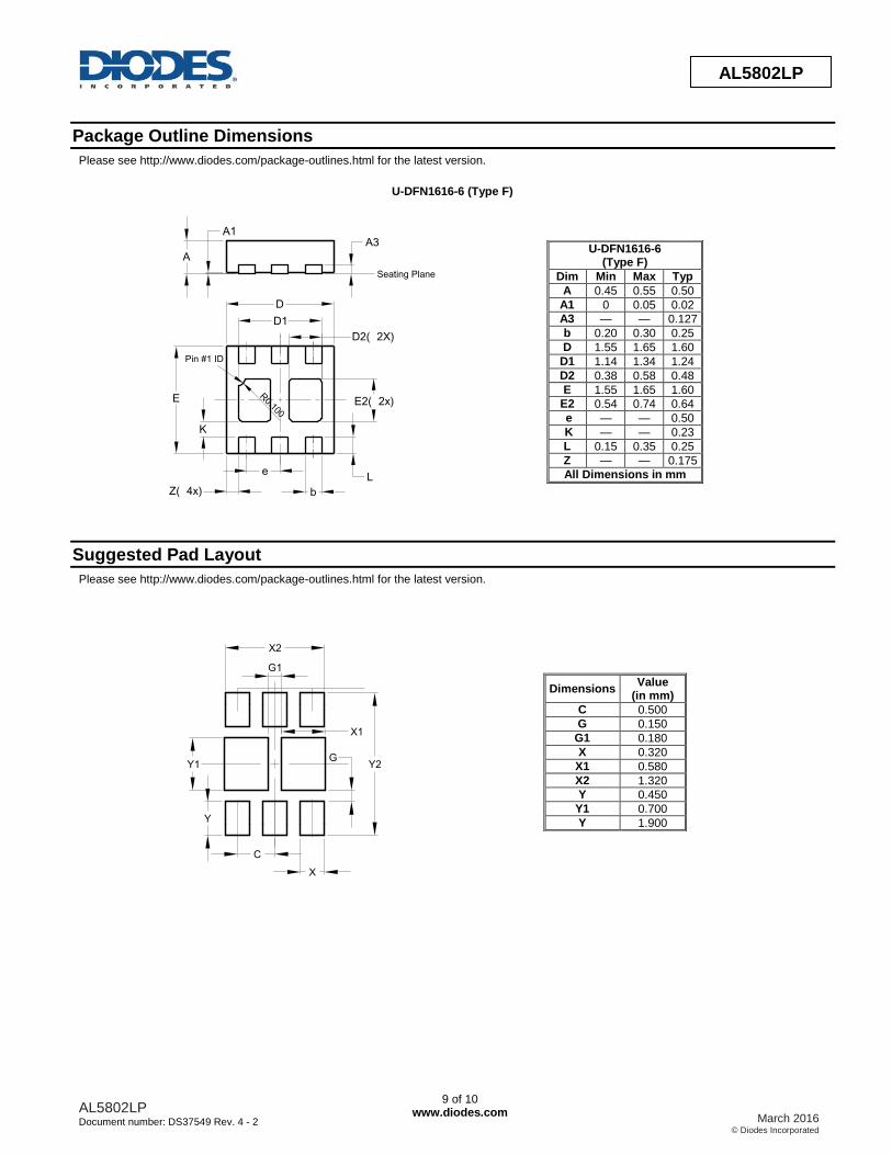
Package Outline Dimensions
Please see http://www.diodes.com/package-outlines.html for the latest version.
U-DFN1616-6 (Type F)
Suggested Pad Layout
Please see http://www.diodes.com/package-outlines.html for the latest version.
U-DFN1616-6 (Type F)
Dim Min Max Typ
A 0.45 0.55 0.50
A1 0 0.05 0.02
A3 — — 0.127
b 0.20 0.30 0.25
D 1.55 1.65 1.60
D1 1.14 1.34 1.24
D2 0.38 0.58 0.48
E 1.55 1.65 1.60
E2 0.54 0.74 0.64
e — — 0.50
K — — 0.23
L 0.15 0.35 0.25
Z — — 0.175
All Dimensions in mm
Dimensions Value
(in mm)
C 0.500
G 0.150
G1 0.180
X 0.320
X1 0.580
X2 1.320
Y 0.450
Y1 0.700
Y 1.900
Pin #1 ID
D2(2X)
D1
R0.100
K
D
E
e
b
L
A
A1A3
E2(2x)
Z(4x)
Seating Plane
Y2
X2
Y
C
X
Y1G
X1
G1
AL5802LP Document number: DS37549 Rev. 4 - 2
10 of 10 www.diodes.com
March 2016 © Diodes Incorporated
AD
VA
NC
E IN
FO
RM
AT
IO
N
NE
W P
RO
DU
CT
AL5802LP
IMPORTANT NOTICE DIODES INCORPORATED MAKES NO WARRANTY OF ANY KIND, EXPRESS OR IMPLIED, WITH REGARDS TO THIS DOCUMENT, INCLUDING, BUT NOT LIMITED TO, THE IMPLIED WARRANTIES OF MERCHANTABILITY AND FITNESS FOR A PARTICULAR PURPOSE (AND THEIR EQUIVALENTS UNDER THE LAWS OF ANY JURISDICTION). Diodes Incorporated and its subsidiaries reserve the right to make modifications, enhancements, improvements, corrections or other changes without further notice to this document and any product described herein. Diodes Incorporated does not assume any liability arising out of the application or use of this document or any product described herein; neither does Diodes Incorporated convey any license under its patent or trademark rights, nor the rights of others. Any Customer or user of this document or products described herein in such applications shall assume all risks of such use and will agree to hold Diodes Incorporated and all the companies whose products are represented on Diodes Incorporated website, harmless against all damages. Diodes Incorporated does not warrant or accept any liability whatsoever in respect of any products purchased through unauthorized sales channel. Should Customers purchase or use Diodes Incorporated products for any unintended or unauthorized application, Customers shall indemnify and hold Diodes Incorporated and its representatives harmless against all claims, damages, expenses, and attorney fees arising out of, directly or indirectly, any claim of personal injury or death associated with such unintended or unauthorized application. Products described herein may be covered by one or more United States, international or foreign patents pending. Product names and markings noted herein may also be covered by one or more United States, international or foreign trademarks. This document is written in English but may be translated into multiple languages for reference. Only the English version of this document is the final and determinative format released by Diodes Incorporated.
LIFE SUPPORT Diodes Incorporated products are specifically not authorized for use as critical components in life support devices or systems without the express written approval of the Chief Executive Officer of Diodes Incorporated. As used herein: A. Life support devices or systems are devices or systems which: 1. are intended to implant into the body, or
2. support or sustain life and whose failure to perform when properly used in accordance with instructions for use provided in the labeling can be reasonably expected to result in significant injury to the user.
B. A critical component is any component in a life support device or system whose failure to perform can be reasonably expected to cause the failure of the life support device or to affect its safety or effectiveness. Customers represent that they have all necessary expertise in the safety and regulatory ramifications of their life support devices or systems, and acknowledge and agree that they are solely responsible for all legal, regulatory and safety-related requirements concerning their products and any use of Diodes Incorporated products in such safety-critical, life support devices or systems, notwithstanding any devices- or systems-related information or support that may be provided by Diodes Incorporated. Further, Customers must fully indemnify Diodes Incorporated and its representatives against any damages arising out of the use of Diodes Incorporated products in such safety-critical, life support devices or systems. Copyright © 2016, Diodes Incorporated www.diodes.com